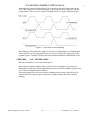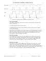
1
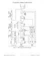
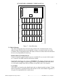
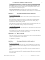
i
CCD DRIVER ASSEMBLY USER MANUAL
CCD CAMERAS
CCD DRIVER ASSEMBLY
CDB01-x
User Manual
11 April 2007 Alan Stummer
This manual only applies to the attached pair of boards in the chassis, the Digital and
Analog boards. It does refer to the Buffer board (the little one in the vacuum box) and
the Headboard (the U-shaped one that actually holds the CCD). This manual does not
recognize that the Digital/Analog boards are in a chassis. See Page 4.
'© Marconi Applied Technologies Limited 2000.This work must not be copied in whole or in part without the
prior written permission of Marconi Applied Technologies Limited.'
© Marconi Applied Technologies Limited 2000
1
A1A-CDB01-x Issue 3, 23/03/07
CCD DRIVER ASSEMBLY USER MANUAL
Congratulations on buying this high quality
Marconi Applied Technologies product!
The Marconi Applied Technologies CCD driver assembly facilitates high performance slow scan
operation of Marconi Applied Technologies Scientific CCD sensors. It has been designed with as
much flexibility as possible and drives most of Marconi Applied Technologies’s CCD02, CCD05 or
CCD15 series CCD sensors.
High quality, multi-layer PCB’s are used, with separate power & ground planes. The PCB’s are
populated with a combination of discrete and surface-mount components, all of good commercial
grade.
Particular attention is paid to minimise interaction between low level analogue signals and high
power digital drive pulses, as well as their associated supply rails. This is achieved by PCB layout,
extensive decoupling and individual voltage regulation.
All cables are screened and use shielded connectors.
Logic generation is achieved by the use of a Field Programmable Gate Array (FPGA, also referred to
as ERA). The FPGA draws its code from an EPROM, which contains drive information for
12 Marconi Applied Technologies CCDs. As Marconi Applied Technologies introduces new
scientific CCDs, the EPROM is updated accordingly, thus ensuring that the CCD driver assembly
provides the most up to date drive waveforms for Marconi Applied Technologies CCDs.
The driveboard supplied has the latest issue of EPROM. Future issues of EPROM can be ordered
separately as they become available.
FEATURES
♦ slow scan operation for very low readout noise
♦ ‘remote head’ for ease of installation
♦ switch adjustment of readout modes
♦ full frame, frame transfer and TDI modes
♦ pixel & line binning
♦ readout rates from 50 kHz to 1 MHz
♦ remote operation via Centronics port
♦ potentiometer adjustment of clock amplitudes, bias, offset etc
♦ link adjustment of CCD sample and clamp timing
♦ generous test points for confirmation of satisfactory operation
♦ synchronization signals for framestore
© Marconi Applied Technologies Limited 2000
2
A1A-CDB01-x Issue 3, 23/03/07
ii
CCD DRIVER ASSEMBLY USER MANUAL
♦ ramp generation for X Y Z oscilloscope display
♦ matching rack and PSU available
♦ optional setup service for a particular CCD
© Marconi Applied Technologies Limited 2000
3
A1A-CDB01-x Issue 3, 23/03/07
iii
CCD DRIVER ASSEMBLY USER MANUAL
This Manual
This manual describes the basic operation of the CCD Driver Assembly, and should provide all
the information required to set up the CCD Driver Assembly with any sensor. The reader will
need to have familiarity with basic electronic principles to fully understand this manual.
The CCD Driver Assembly
There are three types of CCD Driver Assembly: CDB01-1, CDB01-2 and CDB01-4; with: one,
two and four video channels respectively. The CDB01-1 is described in detail in this manual as
it is the most commonly used.
The CCD Driver Assembly is used with a sensor and its associated headboard (CHBxx-xx),
which must be ordered separately, to make a CCD camera system. A rack (CDR01) with a
triple voltage power supply (CDP01) is available so that the system can by powered from the
mains.
Setting up problems
If there are problems when setting up the CCD Driver Assembly which are not covered in this
manual, contact MARCONI APPLIED TECHNOLOGIES for technical assistance. Do not
change components or modify any circuit boards. The multi layer circuit boards can be easily
damaged by incorrect rework.
Displaying an image
The CCD Driver Assembly is intended for use with a framestore which can capture and display
images with high resolution. To help in preliminary assessment however XYZ circuitry is
included for picture imaging on an oscilloscope (in XYZ mode).
IMPORTANT
The CCD Driver Assembly contains static sensitive components:
Always observe antistatic precautions when handling the circuit
boards of the CCD Driver Assembly - this also applies to the CCD
sensor and headboard (CHBxx-xx).
For further details see section 1 Anti-static precautions.
© Marconi Applied Technologies Limited 2000
4
A1A-CDB01-x Issue 3, 23/03/07
iv
CCD DRIVER ASSEMBLY USER MANUAL
1. Anti-static Precautions
1.1. Introduction
All circuit boards which make up the CCD Driver Assembly contain static sensitive
components. CCD sensors are particularly susceptible to static damage.
British standard BS EN100015-1:1992 gives full details on anti-static precautions. These
are the basic precautions that must be observed:
1.1.1.Packaging
All components are supplied in black anti-static bags, and should be kept in
these bags until required. When components are removed from the bags, full
anti-static precautions must be observed. When returning components to
Marconi Applied Technologies they must be sent in anti-static bags.
1.1.2.Workstation
A bench should be set aside as an anti-static workstation, with a bench mat, floor
mat, strap to earth and wrist strap. The CDB components should be unpacked,
handled and assembled only at the anti-static workstation with the handler
wearing the wrist strap.
If camera components need to be handled in a remote location the handler must
wear a wrist strap attached to earth, and keep the components in anti-static bags
where possible.
© Marconi Applied Technologies Limited
1......................................................A1A-CDB01-x Issue 3 23/03/07
1
CCD DRIVER ASSEMBLY USER MANUAL
Figure 1 – Schematic of Drive Board Assembly
© Marconi Applied Technologies Limited
2......................................................A1A-CDB01-x Issue 3 23/03/07
2
CCD DRIVER ASSEMBLY USER MANUAL
2. Introduction to the CCD Driver Assembly
The schematic shows the three circuit boards which make up the CCD Driver Assembly and
their interconnections. The three boards are described briefly below:
2.1. The Digital Board
This board houses the control logic for the CCD sensor and the video processing, and is
also responsible for interfacing with the outside world. The Digital Board sends control
pulses to the Analogue Board via the 20 way piggyback connector, and to the Buffer
Board via the two metre 37 way ribbon cable. The 64 way (a and c) DIN 41612
connector is where power is fed into the CCD Driver Assembly and where the control
and synchronisation signals enter and leave.
2.2. The Buffer Board
This board terminates the logic signals from the Digital Board to the sensor and amplifies
the output signal from the sensor on the headboard. The sensor signal is sent via a miniCOAX cable to the Analogue Board.
2.3. The Analogue Board
This board processes the sensor signal from the Buffer Board using correlated double
sampling to give analogue video, with adjustable gain. The video signal can be linked to
a BNC connector on the front panel or to a pin on the DIN 41612.
2.4. Centronics Program Disk
In addition to the three boards mentioned above and the two cables, a disk is also
supplied with the CDB. The CDB Menu program enables computer control of camera
parameters (described later in this manual).
© Marconi Applied Technologies Limited
3......................................................A1A-CDB01-x Issue 3 23/03/07
3
4
CCD DRIVER ASSEMBLY USER MANUAL
+5 V
F1
DEVICE SELECT
SWITCHES
+15 V
9 MHz
CLOCK
EPROM
F2
F3
LCL/CMP
SWITCH
-15 V
FRONT PANEL
LED
TP
19
2
23
3
25
4
24
5
22
8
1
AR 1
ERA
CONFIGURE
CIRCUIT
SWITCH
TP
18
AR 2
SW5
B/AR 3
BR 2
31 SWITCHES
BR 1
A/B R
LATCH
ERA
DATA
CONTROL
12 OFF SHAPER BUFFERS
FPGA
10
A 1
INIT
14
A 2
ERROR
11
STATUS, SYNCS
DIN
41612
A 3
CONTROL SIGNALS
15
B 1
36 V
CHARGE
PUMP
TP17
TP6
TP7
TP9
TP13
TP20
12
B 2
16
B 3
36 V
SUPPLY
FIL 1,2
GAIN 1,2
DIFFERENTIAL
DRIVERS
VR4
PIXCMP, PIXSMP, R, C R
DIN
41612
PIXCMP, PIXSMP, R, C R
TP 31 33 34 35 36
VEE
(-3 V)
SENSOR SUPPLIES
TP29
VSS
VR7
TP28
TP30
VOD
VR8
TP32
VR6
0V
TP26
VDD
VR3
V
TP27
VRD
VR2
TP21
VOG
VR5
VDG
VR1
E RA .A P FF G 2 1 Fe br u ary
19 94
Figure 2 – CDB Digital Block Diagram
© Marconi Applied Technologies Limited
4......................................................A1A-CDB01-x Issue 3 23/03/07
CCD DRIVER ASSEMBLY USER MANUAL
3. How it works
3.1.
Introduction
This manual describes in detail how to set the various switches and adjustments on the
CCD Driver Assembly. To put the various functions in context it is useful to have an
overview of how the camera works.
3.2.
The Digital Board
The ERA is a field programmable gate array which controls operation of the CCD Driver
Assembly and its sensor. A 9 MHz crystal oscillator provides the ERAs master clock.
The ERA has to be 'configured' on start up - all its set up data is stored in the EPROM.
Four of the EPROMs address lines go to switch 6, hence the data loaded into the ERA
depends on the setting of this switch: the control data for the 12 different sensors can be
stored in the EPROM.
If switch 6 is adjusted, the ERA will need to be reconfigured to load new data. To
reconfigure while powered up, use the ‘reset’ switch (switch 5). Switch settings will be
discussed in more detail later.
The ‘config’ LED on the front panel lights to show that the ERA is configured.
To enable the camera to operate in different modes (eg. readout rate, full frame) there are
31 parameter switches connected into the ERA (all but one way of 8 way switches 1 to
4). Parameter access to the ERA is designed so that latched parameter settings can
override the switches, under control of the centronics interface (part of the DIN 41612
connector).
The ERA supplies pulses to the charge pump circuit which supplies 36 V at a low current
for various bias voltage circuits.
The various charge transfer (‘ ’) pulses from the ERA are shaped and buffered to the 37
way cable and the buffer board. VR6 sets the upper voltage of all the waveforms.
The six CCD bias voltage circuits are on the Digital Board, the presets and test points are
shown. When probing the test points hook the probe earth onto one of the six 0 V test
points shown.
© Marconi Applied Technologies Limited
5......................................................A1A-CDB01-x Issue 3 23/03/07
5
CCD DRIVER ASSEMBLY USER MANUAL
Figure 3 – CDB Analogue Board Block Diagram
© Marconi Applied Technologies Limited
6......................................................A1A-CDB01-x Issue 3 23/03/07
6
CCD DRIVER ASSEMBLY USER MANUAL
3.3. The Buffer Board Is this just a typo, see 3.4?
This board has an amplifier with adjustable gain; links 1, 2 and 3 give gains of 4,8 and 16
3.4. The Buffer Board
This board has an amplifier with adjustable gain; links 1, 2 and 3 give gains of 4,8 and 16
respectively. The sensor signal is sent via the SMC connector to the Analogue Board.
3.5. The Analogue Board
The sensor signal is processed on the Analogue Board using ‘correlated double
sampling’.
The first gain stage has adjustable gain via two position switch 1, ‘1’ gives ×1 and ‘0’
gives ×4. A low pass filter follows the first gain stage to filter out pixel frequency noise.
When the pixel readout rate is changed the FIL1 and FIL2 lines adjust the low pass cut
off frequency.
VR5 adjusts the video black level at the pixel rate clamp. The phase of the pixel clamp
signal can be adjusted by moving between links 9, 6, 11, 6, 13 and 8. Similarly at the
pixel sample stage, phase can be adjusted by moving between links 15, 10, 16, 12, 17 and
14.
The gain of the output stage is under control of parameter switch 2 on the Digital Board.
Gain can be set to 1, 2 or 4. The output video signal can be linked to the DIN 41612
connector (link 18A) or the BNC on the front panel (link 18B).
The X and Y ramp circuits generate line and field ramps for display of an image on an
oscilloscope in XYZ mode. The Z amplifier inverts and amplifies the analogue video,
suitable for modulating the oscilloscope beam intensity.
© Marconi Applied Technologies Limited
7......................................................A1A-CDB01-x Issue 3 23/03/07
7
CCD DRIVER ASSEMBLY USER MANUAL
4. Start up Routine
4.1. Introduction
This section of the manual gives an overview to setting up the CCD Driver Assembly and
also aims to explain the most rapid route to achieving an image. It only considers the
most basic operation ie. fixed settings, un-cooled, full frame operation with visible light.
Subsequent sections of the manual go into detail allowing the full flexibility of the board
to be utilised.
Items supplied with the CCD Driver Assembly
♦ Driver Board consisting of digital and analogue boards
♦ Buffer Board
♦ Two metres of 37 way screened shielded ribbon cable with Cannon “D” connector on
each end
♦ Miniature coax cable terminated with SMC connectors either end, two metres long
♦ Manual
♦ Centronics driver program disk
Items required to complete an imaging sub-assembly (ordered separately)
♦ Marconi Applied Technologies CCD sensor
♦ Headboard
Items of equipment that will be required to set up and run the driver board
♦ Signal generator or timer that will produce a 5 volt pulse equal to the desired
integration time.
♦ Lens or other optical arrangement to focus image onto CCD
♦ Shutter arrangement or pulsed illumination (essential for full frame imaging)
♦ DIN 41612 64 way female connector (the CDR01-1 eurocard rack is recommended)
♦ Power supplies, +15 V, +5 V, -15 V (the CDP01 is recommended)
♦ Shutter (or LED) supply
♦ Slow Scan Input Framestore (with built-in ADC)
♦ Oscilloscope
♦ Voltmeter
♦ PC with parallel printer port (optional)
Overview of Setup
Observe antistatic precautions
Unpack boards and cables
Do NOT adjust switches or potentiometers on CDB01 if Setup was ordered
If Setup option was not ordered, select CCD type, mode of operation and be prepared
to adjust the CCD bias voltages for best image
♦ Connect CCD headboard with short ribbon cable to buffer board
♦ Connect CDB01 with two metre, 37-way ribbon cable to buffer board
♦ Connect the front panel BNC on the CDB01 to channel A of an oscilloscope
♦
♦
♦
♦
© Marconi Applied Technologies Limited
8......................................................A1A-CDB01-x Issue 3 23/03/07
8
9
CCD DRIVER ASSEMBLY USER MANUAL
♦ Connect line drive/line sync on the 64-way DIN41612 to channel B of the
oscilloscope
♦ Trigger off channel B
♦ Focus an image with light level of about 50 millilux on the CCD
♦ If at all possible, operate the CCD in frame transfer mode
♦ Connect DIN41612: apply power to CDB01 - look for green LED on CDB01 front
panel
♦ Observe the waveform on channel A of the oscilloscope. This should have an
amplitude of about 0.5 to 2.0 V peak-peak, with modulation corresponding to the
scene being imaged
♦ Connect video, frame, line and pixel clocks to framestore - obtain image on computer
4.2. Power Supply Requirements
The power supply must be a linear regulated type - do NOT use a switched mode
type.
Parameter
5V
+15 V
-15 V
5.0 to 5.2
+15.0 to +15.5
-15.0 to -15.5
Typical current (mA)
200
600
200
Peak current (mA)
400
1200
400
PSU current limit (A)
1.0
1.5
1.5
Maximum ripple (mV)
3
5
5
Voltage (V)
4.2.1.Connection of Power to CDB01-1 Driver Board
A DIN41612 64-way socket, (rows A and C) is required.
The pinout of this connector is shown in Appendix B. Power rails are input on pins
28 to 32 rows A and C.
4.3. Positioning the camera head
The camera head is in two parts, the CCD Headboard and Buffer board. Each type of
CCD has a unique Headboard but the Buffer board is common to all types of CCD. The
Headboard may be mounted within the optical system by the mounting holes as shown in
Appendix H, which also shows the position of the CCD centre and focal plane with
respect to all of the CCD boards.
The Buffer board is also fixed by mounting holes as shown in Appendix H. It is
connected to the CCD board by a 26 way ribbon cable and must be not more than 50 mm
from the CCD board. Prior to mounting the Buffer board it is recommended that gain of
the buffer amplifier be set by selecting the appropriate link.
Channel
1
© Marconi Applied Technologies Limited
Link
LK4
LK5
Gain
4
8
Comments
9......................................................A1A-CDB01-x Issue 3 23/03/07
CCD DRIVER ASSEMBLY USER MANUAL
2
3
4
LK6
LK1
LK2
LK3
LK10
LK11
LK12
LK7
LK8
LK9
16
4
8
16
4
8
16
4
8
16
This channel normally
used for low noise
output
This channel normally
used for low noise
output
For a single output device CHANNEL 2 of the headboard will be connected to
Channel 1 of the Analogue board.
For CCD15 series all outputs are low noise.
Set gain as appropriate for device type. Devices having large pixel area will require a lower
gain setting. In any case, the gain should be chosen to ensure that the video input level to the
Analogue board does not exceed 5 volts when the CCD output is saturated.
Do not connect headboard to digital board at this stage.
© Marconi Applied Technologies Limited
10.....................................................A1A-CDB01-x Issue 3 23/03/07
10
CCD DRIVER ASSEMBLY USER MANUAL
4.4. Pulsed or Shuttered Illumination
When using full frame CCDs, the issue of whether or not to use pulsed or shuttered
illumination must be considered. In practice, this only becomes essential when the
readout time is longer than the integration time.
In many cases, particularly when the dark current in the CCD is limited by the use
of an inverted mode CCD, and/or the use of an external Peltier cooler, the
integration time can be made relatively long. In this case, the readout time,
especially if 1 MHz rate is used, may be at least a factor of three shorter than the
integration time. Whilst there will be some evidence of frame shift smear, the
resultant image will be very usable. Accordingly, pulsed or shuttered illumination is
often not required, although for the best results, instructions on how to achieve this
is given below.
If illumination is provided by an artificial source then it might be appropriate to pulse this
source using a circuit similar to that shown below. Where the scene is naturally illuminated it
will be necessary to place a suitable shutter between CCD and scene. In order to be compatible
with the board, the scene should be illuminated or the shutter open when the input to the
illumination control is high.
It is advantageous (to prevent feed through of spikes onto the driver board) to power the
shutter/light source from a separate supply and use a buffer from 5 volt CMOS to the shutter
supply. A suitable circuit for shutters that consume up to 1 amp at between 5 and 25 volts is
shown below.
Figure 4 Shutter Buffer
Timing
The shutter/light source must be synchronised to the CCD Driver Assembly.
For initial evaluation purposes it is acceptable to connect the input of the shutter control to
Pin 19C on the 64 Way DIN 41612 connector on the rear of the digital board. In this
configuration the integration time must be at least 10 times greater than the shutter's response
time. (Typically 20 ms for a mechanical shutter.)
See Appendix B for a list of inputs and outputs on the DIN 41612 connector. Pin 19C is Start
Integration and goes high for the duration of integration. Under normal operation it closely
follows the level of Request for Integrate (Pin 20C), the timing input to the board.
© Marconi Applied Technologies Limited
11......................................................A1A-CDB01-x Issue 3 23/03/07
11
CCD DRIVER ASSEMBLY USER MANUAL
4.5. Power supplies
All power supply voltages should be ± 2% of the stated value, and free of ripple
+5 volts at 400 mA to pins 29A & 29C When the board is turned on or reset, it
consumes up to 1 amp at 5 volts for up to 30 ms
during reconfiguration. At all other times,
regardless of mode of operation, the power
consumption is as stated.
+15 volts at 500 mA to pins 28A & 28C During frame transfer the board consumes up to
2 amps at 15 volts for the duration of the frame
transfer. Current demand also increases as the
number of binned lines is increased, up to a
maximum of 2 amps when 256 lines binned
-15 volts at 300 mA to pins 30A & 30C
Power supply ground to pins 32A & 32C
It is important to ensure that either all supplies are connected simultaneously, or
+5 volts applied first.
4.6. Select device and set bias supplies
The board set up includes the selection of CCD type, drive mode and adjustment of all
DC supplies to the CCD.
Use Switch row 6 to select the type of CCD that is being driven, eg, CCD 05 - 30, 02 06 etc. See Appendix D for CCD types and their respective switch positions.
Refer to Appendix C for setting of the switch array (Switch rows 1 - 4). The switches
may be set directly or remotely by a PC with the software provided. For initial operation
it is best to set the switches manually and then change them as desired using the remote
selection.
If the remote selection is to be used the typical suggested initial manual settings are:
Line and pixel binning.
(Rows 3 and 4)
All switches set to 0 or off.
Directions and Gain.
(Row 2)
Set switches e & f to 1 or on,
Set rest of row to 0 or off.
Readout rate and mode
of operation. (Row 1)
Switches set as required.
Now that the CCD type and mode of operation have been selected all of the DC supplies
need to be checked and if necessary, adjusted to the requirements of the selected CCD
before the board can be connected to the headboard and CCD.
Turn on the power to the board. The supplies should be switched on simultaneously or 5
volt supply first.
© Marconi Applied Technologies Limited
12.....................................................A1A-CDB01-x Issue 3 23/03/07
12
CCD DRIVER ASSEMBLY USER MANUAL
When the 5 volt supply is turned on check to see that the green LED on the front panel is
illuminated. This confirms that the ERA has configured correctly. See troubleshooting if
LED does not light.
Refer to appendices F G and H, for a list of bias adjustments, testpoints and
potentiometers, and for the location on the board of the test pins and potentiometers. The
set voltages may be double checked for the correct setting at the respective pin on the 37
way connector to the headboard.
Not all of these potentiometers will need to be set, i.e. VDG is only required on a few
devices i.e. on the CCD 25 series and VCP is set at 36 volts and must not be adjusted. At
this stage only the voltages listed in Appendix G can be set. Going around the bias points
as listed, connect a voltmeter across the test pin listed and TPs 31, 33, or 34 (Ground)
and rotate the respective potentiometer until the desired voltage is reached. Once all bias
voltages are set turn off the power to the board.
If the remote switch selection is to be used connect the parallel printer port of a PC to
pins 1 to 13A and 1 to 13C of the DIN 41612 via 25 way ribbon cable where pin 1 of the
25 way Cannon 'D' corresponds to pin 1C on the DIN 41612, pin 2 corresponds to pin
1A, 3 to 2C etc. One method of connecting the 25 way ribbon cable to the DIN 41612 is
to use a 41612 socket with wire wrap pins (soldered through a backplane) and terminate
the 25 way ribbon cable with a 26 IDC backplane connector manufactured by 3M and
supplied by ESD.
To operate software turn on computer and CDB, connected as above. Insert supplied disk
into drive, select that drive and type CDB. You will be presented with a list of options.
Use cursor keys to select option and return to toggle option. When settings are as desired
place cursor on send and press return.
© Marconi Applied Technologies Limited
13.....................................................A1A-CDB01-x Issue 3 23/03/07
13
CCD DRIVER ASSEMBLY USER MANUAL
4.7. Integration control pulse
Do not allow the output of the signal generator in to the digital board go high if the
board is not powered as this may result in damage.
Connect output of a signal generator/timer between pins 20C on the DIN 41612, request
for integration and pins 32A & 32C, ground.
The clock into the board must be either TTL or 5 volt CMOS. The board will start
integration on the rising edge of this pulse and commence readout on the falling edge. ie.
The integration time of the CCD is equal to the high duration of the clock from the signal
generator. The clock should then be held low long enough for the CCD to be read out. If
the request for integration line is taken high before the CCD has been read out then the
rising edge is ignored until the board has completed out the last frame.
The readout time for the CCD can be calculated from the CCD data sheet or from
Appendix E, using the following approximate equation.
TRO =
where: TRO
L
P
BL
RR
=
=
=
=
=
L x ( P + 3)
( BR x RR )
Readout Time.
Total number of lines on CCD (Vertical Elements)
Total number of pixels in Readout Register
No of binned lines. ie. 1 for no binning, 2, 3 etc.
Readout Rate.
Alternatively the readout time can be monitored at the Grab output from pin 18C of the
DIN 41612, which is LOW during readout of the CCD.
The actual integration time can be monitored at pin 19C, start integrate, which is HIGH
during integration. This pulse will normally be the same width as request for integrate
(Pin 20C) unless request for integrate is high during the readout of the CCD, in which
case start integrate, and hence integration interval, will be shortened.
4.8. Connect buffer board & headboard to digital board
Now that all of the bias voltages have been checked and board connected to integration
control pulse, turn off the power to the board and connect the headboard. The two are
connected by up to 2 metres of 37 way screened ribbon cable and 1 to 4 RG174 coaxial
cables, one cable per video channel, each up to 2 metres long.
4.9. Set video pedestal and gain on the Analogue Board
Setting up of the analogue board involves setting the gain of the video processing such
that the video output is of the desired level and adjusting the pedestal or voltage to which
the reset level is clamped. The gain is set at three stages of the video path. First the buffer
board, then the input to the CDS circuit and finally the output stage of the CDS circuit.
The gain of the output stage may also be adjusted remotely.
© Marconi Applied Technologies Limited
14.....................................................A1A-CDB01-x Issue 3 23/03/07
14
CCD DRIVER ASSEMBLY USER MANUAL
The following operations will need to be performed on each video channel used, apart
from setting final stage gain which is common to all channels. Note that the Z output for
XYZ operation is only available on channel 1.
Gains of ×4, ×8 or ×16 are available on the buffer board, and should have been set
previously as indicated in paragraph 1 - positioning of the headboard.
Switch 1 provides gains of ×1 or ×4 at the input of the CDS circuit and the two gain
switches on the digital board provide gains of ×1, ×2, ×4 or ×8 at the output of the CDS
circuit.
Turn on power to the system. ie. Board, signal generator and illumination/shutter, so that
the system is operating as desired.
Connect a scope probe between test pin 1 (video signal) and test pin 20 (Ground). See
Appendix F for location of test pins, on boards and in the circuits. With the CCD under
peak predicted illumination, check the video amplitude at TP1.
Trigger the oscilloscope from either edge of the pixel clock (Pin 15C) The waveform
you should expect to see during readout is shown here.
Figure 5 – CCD Output Waveform
This best represents the waveform at 50 kHz readout rate. At higher frequencies it
becomes more rounded.
The mean reset level at TP1 should be 0 volts. The difference in signal level and reset
level, the signal, at TP1, is influenced by all of the following variable elements.
Incident illumination at CCD
Lens aperture
Intensity of light source
Integration time of CCD
Gain set on buffer board
Gain set at switch 1 on analogue board
All of the above should be adjusted to set the signal at TP1 to the desired level of video up to a maximum of 5 volts. It is possible that there will not be enough light available to
achieve the desired output video amplitude at the preferred integration interval. In this
© Marconi Applied Technologies Limited
15.....................................................A1A-CDB01-x Issue 3 23/03/07
15
CCD DRIVER ASSEMBLY USER MANUAL
case set the gain on the buffer board to ×16 and the gain at switch 1 of the analogue
board to ×4.
The amplitude of the reset feedthrough spikes is not important as the analogue board is
designed to cleanly clip anything over 5.3 volts.
Connect an oscilloscope to the output of the analogue board. (BNC connector J5) Use the
final stage gain switches (switches e and f in row 2 of the switch array) to adjust the
amplitude of the output video to the desired level up to a maximum of 10 volts.
For levels in excess of 1 volt peak this output must not be terminated at the
ADC/framestore.
Now the pedestal should be adjusted. Use the output from pin 17 C to trigger the
oscilloscope which should still be connected to the output of the analogue board. Ensure
that the CCD is not illuminated. Adjust the pedestal pot listed in Appendix F until the
video output is at 0 volts or desired pedestal. This is best done using the dark reference
elements. The dark reference elements are those that are read out while line clamp is
high. This will be two or three pixels at the start of each line for 05 series CCDs.
Checking of Dynamic Range
Set link 18 of the analogue board to route the video output to the BNC socket on the
front panel. Connect the BNC via a 50 ohm coaxial cable to the channel 1 input of an
oscilloscope using a 'T' piece, and 50 ohm termination resistor. Connect a scope probe to
channel 2 and attach this to pin 15C (pixel clock) of the 64 way DIN connector. Trigger
the scope from channel 2. Illuminate the CCD to saturation level and note the amplitude,
in volts, from ground to the peak of the output. See figure 5. Blank off the CCD from all
illumination and on the most sensitive range of the scope note the peak to peak amplitude
of the noise.
Dynamic Range =
6 x peak output
pk − pk noise
4.10.Connection of board to Display Device
The resultant video may be put into an ADC/frame store or the XYZ of an oscilloscope
or suitable monitor.
The choice of display device will depend on whether the intended use needs to generate a
two dimensional image, or provide video data direct into a microcomputer (machine
vision) or merely provide an output voltage proportional to light input (as is the case
when the CCD is used to replace a photomultiplier, for instance).
In all cases, a slow scan input frame store will make best use of the video from the driver
board assembly. However, where imaging is not required in the final application, and to
save the cost of a framestore, the driver board can generate a set-up grade image on an
XYZ oscilloscope.
4.10.1.Output to a Framestore
Refer to Appendix B to decide which outputs on the DIN 41612 connector
may be suitable for use with the chosen frame store. The relevant pulses for
framestore use are listed under "Sync Pulses". Refer to section 3 for an
© Marconi Applied Technologies Limited
16.....................................................A1A-CDB01-x Issue 3 23/03/07
16
17
CCD DRIVER ASSEMBLY USER MANUAL
explanation of each clock output waveform, and timing diagrams. Typically
the framestore will require 3 timing pulses:
18C
Grab Frame Clock & Blanking
17A
Blank Line Clock & Blanking
15A&C C
Pixel Clock
Low During Active frame
Low During active line
Active High, both edges valid
Each video channel has an output impedance of 50 ohms.
It may be necessary to include a line clamp. This is a pulse on pin 17C that is
high during the readout of dark reference elements at the start of a line of
video.
Use supply ground as a signal return for the above signals.
Turn on all power to view image. When turning on power to the system,
always turn on the board before any inputs to the board (except computer
interface).
4.10.2.Output to an Oscilloscope
The X, Y and Z outputs will need to be adjusted. Refer to Appendix F for
locations of potentiometers to adjust. Connect X and Y outputs to oscilloscope.
Ensure that links 1,3,4 and 5 are in place.
Turn on power to the board. To set the X ramp, hold the input from the signal
generator, request for integrate, low.
Look at the output from X on the scope. Use either edge of line blank (Pin
17A) to trigger the oscilloscope. The trace observed on the oscilloscope should
resemble that in figure 6.
Line/Frame Duration
Line f ra m .1 FFG 1 3 Ap ril 1 994
Figure 6 – Output from X and Y
Adjust potentiometer VR1 such that the amplitude of the waveform is around 8
to 10 volts.
To adjust Y, the signal generator must be set to provide Request for Integration
input pulse to stimulate the board to readout the CCD. For this purpose set the
output of the signal generator to a rate in the order of 10 Hz, 50% duty cycle
square wave.
The traces produced should resemble those shown for X ramp as in figure 3,
but having a longer duration (TRO as calculated earlier). Use the falling edge of
© Marconi Applied Technologies Limited
17.....................................................A1A-CDB01-x Issue 3 23/03/07
CCD DRIVER ASSEMBLY USER MANUAL
grab to trigger the oscilloscope. Adjust potentiometer VR 2 such that the peak
voltage of the waveform is around 8 to 10 volts.
For longer readout times move the header from link 1 to link 2. This reduces
the rate of increase in voltage on the Y ramp thus making adjustment easier,
using the same potentiometer.
The Z axis output will need to be set. This output is tailored for the beam
modulation control inputs for oscilloscopes, hence the Z output is inverted
video with a large positive offset.
While there is still no illumination on the CCD, adjust VR6 so that the voltage
at the output of Z is equal to the trace blanking voltage for the oscilloscope.
Illuminate the CCD at normal operational level and adjust VR5 (Z amplifier
gain) so that the peak video signal just goes down to 0 volts. If there is
insufficient gain, increase the gain at the final stage of the CDS board. This
output is now ready to be connected to the beam modulation input of the
scope.
To use the oscilloscope to view an image, connect X to X channel on scope, Y
to Y and Z to beam modulation input. Switch the scope to XY mode. Set the
sensitivity of X and Y channels on scope to 1 volt per division. Adjust X and Y
position controls and trace intensity until image is central on scope screen.
This method of viewing does not maintain the aspect ratio of the image. It may
be restored by adjusting the X and Y channel sensitivities on the scope.
5.
In Depth Circuit Description and Operation
This section of the manual describes in detail the operation of the digital board and analogue
board. Function and operation of the head board assembly is described in the next section. This
section is split into the following subsections.
Power Supplies
A brief description of power supply requirements.
DC Bias Supplies
This subsection describes how to optimise the performance of the CCD using the bias supplies.
Mode selection
Describes the modes of operation that are available and the switch array settings required to
select the mode of operation.
© Marconi Applied Technologies Limited
18.....................................................A1A-CDB01-x Issue 3 23/03/07
18
CCD DRIVER ASSEMBLY USER MANUAL
DIN 41612 Backplane connector
Describes all the control lines present at the 64 way connector and their uses. This covers all
the inputs required by the board for correct operation and outputs that may be used to
synchronise the video output of the board to the receiving system.
Video Processing
Describes the video processing and how to adjust the output video to that required by the
receiving system.
5.1. Power Supplies
The power requirements of the board are:
+15 ± 0.5 volts, ripple free, at a maximum of 1 amp
+ 5 ± 0.2 volts, ripple free, at a maximum of 1 amp
-15 ± 0.5 volts, ripple free, at a maximum of 0.5 amp
It is important to ensure that either all supplies are connected simultaneously, or
+5 volts applied first.
All power supplies must be regulated and have a low impedance path to the board.
The digital board is fitted with fused over voltage and reverse voltage protection. If the board
is incorrectly connected to the power supplies, then the fuse and input protection diode will
need to be replaced for that supply. All power supplies are filtered for HF noise at the input of
the board.
5.2. DC Bias Supplies
The correct voltages must be set prior to connection to the CCD Headboard. Failure
to observe this precaution may result in irreparable damage to the CCD.
The digital board provides adjustment for all of the voltages required for correct
operation of the CCD, including clock amplitudes. Since the board will support many
different variants it is necessary to ensure that the set voltages are appropriate for the
CCD in use.
The regulated 36 volts that powers some of the DC supplies is factory set and should not
be adjusted. The remainder of the supplies may be set in any order.
VOD
CCD Output transistor drain bias voltage. This voltage is not critical for
optimum performance of the CCD. It should be at least 5 volts higher than VRD.
Set to value in data sheet ± 0.5 volt.
VDD
Diode drain bias voltage. The diode drains are positioned at the extremities of
the active part of the CCD. They drain away any surplus charge generated at the
edges of the active array and any spurious charge generated in the silicon around
the active part of the CCD. Voltage level not critical. Set to value in data sheet.
© Marconi Applied Technologies Limited
19.....................................................A1A-CDB01-x Issue 3 23/03/07
19
CCD DRIVER ASSEMBLY USER MANUAL
VSS
Substrate Supply. This is the voltage to which all other voltages on the CCD are
referenced. This voltage has a significant effect on the performance of the CCD.
Set initially to the figure in the data sheet. This voltage may be optimised once a
CCD is present and running.
Increasing this voltage reduces dark current but will ultimately reduce charge
transfer efficiency. Excessive voltage also reduces full well capacity (i.e. Output
signal). To set the optimum level for Vss:
Remove illumination from the CCD and adjust Vss to bring the level of the
dark reference pixels at the start of each line of video as close as possible to
the blank elements at the start of each line. Then illuminate the CCD and
adjust integration interval or source brightness until the video output is just
about to saturate. Increase Vss until the picture just begins to smear. Reduce
Vss slightly so that the smearing just stops.
Repeat these adjustments as necessary until a satisfactory balance is
achieved.
VRD
Reset drain bias voltage. This is the voltage to which the gate of the output
transistor is set to after the previous pixel has been read out. Adjusting this
voltage will have a significant effect on the performance of the CCD as it
determines the working point of the output transistor. If the set voltage is too
high or low then the gain of the output transistor will not be at it's maximum. Set
initially to the voltage in the data sheet and then adjust to obtain peak output
from the CCD (for constant illumination), whilst also optimising limiting
resolution.
VOG
Output gate bias voltage. This supplies the output gate, which lies between the
end of the readout register of the CCD and the base of the output transistor. It
reduces the feedthrough of the clock signals on the readout electrodes to the
output transistor. The voltage is not critical. Set to value in data sheet.
VR
Readout electrode voltage swing. Setting this voltage too high increases dark
current in standard mode devices. It also increases power consumption and
clocking noise onto the output. Setting VR too low reduces charge transfer
efficiency resulting in smear of the image. Set to voltage in data sheet.
VDG
Dump gate voltage. This is only used in a few devices. If not used ignore this
voltage, alternatively set to voltage in data sheet.
© Marconi Applied Technologies Limited
20.....................................................A1A-CDB01-x Issue 3 23/03/07
20
CCD DRIVER ASSEMBLY USER MANUAL
SW5
(On front panel)
Switch 1
Switch 2
Switch 3
Switch 4
SW6
FT/
FF
STD/
INV
READ
RATE
1
READ
RATE
2
READ
RATE
3
STD/
TDI
COMP/
LOCAL
STD/
XRAY
ON
a
b
c
d
e
f
g
h
OFF
A
DIR
B
DIR
R
DIR1
R
DIR2
GAIN
1
GAIN
2
NOT
USED
NOT
USED
ON
a
b
c
d
e
f
g
h
OFF
SW1
SW2
L.S.B.
M.S.B.
ON
SW3
a
b
c
d
e
f
g
h
OFF
BINNED PIXELS
L.S.B.
M.S.B.
ON
SW4
a
b
c
d
e
f
g
h
OFF
BINNED LINES
S W IT CH E S. 1 F FG 13 A p ri l
1 9 94
Figure 7 – Switch Positions
5.3. Mode Selection
Once the CCD type has been selected using switch 6, the selection of mode can be
achieved either locally by the use of switches as above, or remotely by the use of the
Centronics driver program provided. The choice of local or remote mode must therefore
first be set by the position of switch 1g.
Remote Mode (Centronics Driver)
Connect Centronics (parallel printer) port via a suitable 25 way screened cable to pins 1
to 13 of the 64 way DIN connector on the driver board.
Under DOS, load floppy disc and type 'CDBMENU'. The display will show the list of
modes that can be toggled, as well as gain, readout rate and binning values that can be
set. All switch settings from SW1a to SW4h, except SW1g can be set remotely.
Local Mode
All switches are located on the digital board, and are shown in outline in figure 7. Each
mode of operation is explained below with reference to the switch number. Appendix C
also gives an explanation of the switch arrays.
© Marconi Applied Technologies Limited
21.....................................................A1A-CDB01-x Issue 3 23/03/07
21
CCD DRIVER ASSEMBLY USER MANUAL
SWITCH 1a:
FRAME TRANSFER/FULL FRAME
0 : Full Frame
This mode of operation uses the whole area of the CCD to collect light from an image.
Once the CCD has been exposed for the required integration interval illumination
must be removed. The image may then be read out. In this mode the user is required to
provide an input to control integration interval.
Integration is controlled by pin 20C on the DIN 41612 connector, ‘Request for
Integration’. When this pin is held high all the clocks in the image area of the CCD
are stopped and the CCD collects charge.
While the CCD is integrating an image the readout registers are continuously closed to
keep them free of accumulated dark current.
As soon as ‘Request for Integration’ is taken low, the first line of the image is
shifted into the readout register and the line is read out. Successive lines are readout
until the whole frame has been transferred.
If ‘Request for Integration’ is taken high before readout of the frame is complete, it
is ignored until readout is complete. At completion of readout, if request for integrate
is still high, the CCD will start integration as normal. continuously clocked to keep the
CCD free of dark current.
When ‘Request for Integration’ is held low and an image is not being read out, the
image section of the CCD is
In order to avoid vertical smearing of the image, the CCD must not be
illuminated during image read out.
SWITCH 1a:
FULL FRAME/FRAME TRANSFER
1 : Frame Transfer
This mode of operation uses half of the active area of the CCD for imaging. At the end
of integration the stored image is moved down to the bottom half of the active area for
readout. While this image is being read out the top half of the CCD is integrating the
next image. To use this mode of operation, one half of the CCD will need to be
masked. No shuttering is required for this mode.
Integration is controlled by pin 20C on the DIN 41612 connector, ‘Request for
Integration’.
When this pin is held low, the CCD free runs. i.e. The image area integrates for the
time it takes to read out the store section of the CCD. At completion of readout, the
charge accumulated in the image area is transferred to the store section for readout.
After frame transfer, the image section continues integrating. i.e. In frame transfer
mode with ‘Request for Integration’ held low, integration and readout are almost
continuous, only punctuated by frame transfers.
© Marconi Applied Technologies Limited
22.....................................................A1A-CDB01-x Issue 3 23/03/07
22
CCD DRIVER ASSEMBLY USER MANUAL
The minimum integration time is set by the time it takes to read out the store section.
The integration time of the image section may be extended by holding ‘Request for
Integration’ high. Integration will continue until ‘Request for Integration’ is taken
low, at which point frame transfer will be initiated. At completion of frame transfer
the CCD will revert to normal integration.
If ‘Request for Integration’ is held high and read out of the previous frame is
complete the store section will be continuously clocked to keep it free of dark current.
SWITCH 1b:
STANDARD/INVERTED MODE OPERATION
0 : Inverted Mode Operation
This mode of operation should only be selected if the system is driving an inverted
mode CCD.
In this mode all the electrodes in the image area of the CCD are held LOW during
integration. In inverted mode devices this reduces dark current, allowing longer
integration times without cooling the CCD.
Using this mode on standard devices will allow charge to distribute itself evenly over
the active area of the CCD resulting in complete loss of the image.
1 : Standard Mode Operation
This mode of operation may be used with any device, but will increase dark current in
inverted mode devices.
In this mode one in every three electrodes in the image area is held high. The charge
generated from integration is stored under this electrode.
SWITCHES 1c, d, e: READOUT RATE.
These three switches select the rate at which pixels are read out of the readout register.
The rate set is independent of any other features.
See Appendix C for settings.
SWITCH 1f:
STANDARD/TIME DELAY INTEGRATION
0 : Time Delay Integration
This mode of operation is designed to allow extended integration of moving images,
allowing charge to be moved across the image area of a CCD at the same rate as the
image.
TDI only works in full frame, hence when TDI is selected the setting of switch 1a is
ignored.
In this mode of operation the CCD is normally integrating. The image is read out line
by line on request.
© Marconi Applied Technologies Limited
23.....................................................A1A-CDB01-x Issue 3 23/03/07
23
CCD DRIVER ASSEMBLY USER MANUAL
The line readout is controlled by pin 20C on the 64 way DIN 41612 connector. Every
time that this pin receives a rising edge one line is transferred to the readout register
and read out. If ‘Request for Integration’ is held high or low the CCD will just
continue to integrate. While the readout register is being read out all rising edges to
‘Request for Integration’ are ignored.
Great care must be observed when using this mode of operation to avoid loosing an
image due to over loading the CCD with dark current. There is no inherent charge
clearing so dark current will be accumulated until ‘Request for Integration’ is
switched. If the driver board is switched on in this mode or the CCD has not been read
out for a short period before commencing integration then some arrangement should
be made to clear the CCD of accumulated charge. Two suggested methods, both with
the CCD in darkness are:
1)
Switch the driver board to normal mode of operation for at least 2 seconds or
until ready to start integrating with ‘Request for Integration’ held low.
2)
Supply ‘Request for Integration’ with at least as many pulses as there are lines
to clear the CCD of charge and then keep pulsing for time delay integration.
SWITCH 1f:
STANDARD/TIME DELAY INTEGRATION
1 : Standard integration
As selected in other modes of operation.
SWITCH 1g:
LOCAL/COMPUTER
0 : Local
Mode of operation set by switches on board.
1 : Remote/Computer
Allows remote setting of the functions in the switch array by the computer interface
on pins 1 to 13 on the 64 way DIN 41612 connector. If computer is not present, then
the board reverts to the settings on the switches. The computer interface is based on a
Centronics port and will accept data from the parallel printer port of a PC.
SWITCH 1h:
STANDARD/X-RAY
This switch should be set to 1 for visible light and infra red light incident on the CCD
and to 0 for X rays.
When set for visible illumination, the line clamp pulse on pin 17C on the DIN 41612
connector, goes high for the central two pixels on the dark reference elements at the
start of each line. When switched to X ray illumination, the line clamp pulse is moved
to the blank elements before the dark reference elements at the start of each line.
© Marconi Applied Technologies Limited
24.....................................................A1A-CDB01-x Issue 3 23/03/07
24
CCD DRIVER ASSEMBLY USER MANUAL
SWITCHES 2a, b, c, d
These switches set the direction of movement of charge in both halves of the image
section and readout registers. This allows the image to be read out to any corner of the
CCD, two opposite corners or all four corners of the CCD simultaneously. The
number of options available is dependent on device type.
05-11, 15-11 and 02-06 have only one output.
05-*0 series devices have four outputs, two high speed and two low noise. These
devices do not have split readout registers hence only up to two outputs may be
used at any one time. Selecting readout direction gives the choice of using either
high speed or low noise output.
15-*0 series devices have four identical low noise outputs with split readout
registers hence 1, 2 or 4 outputs may be used at any one time.
With split readout, for example to two opposite corners of the CCD, the image is
split in two for readout, hence halving readout time. The image must then be
reconstituted within the framestore.
SWITCHES 2e, f:
GAIN 1 & 2.
These are the final video processing stage gain selection switches for the analogue
board.
SWITCHES 3a-h:
BINNED PIXELS.
The setting of this row of switches determines the number of binned pixels. This
allows improved sensitivity, but will result in reduced horizontal resolution.
To set the number of binned pixels:
1 Subtract 1 from the desired number of binned pixels.
2 Convert this number to binary
3 Set the row of switches according to the binary result, where switch 1
corresponds to the LSB.
Example:
Require 6 binned lines.
Subtract 1 - Left with 5
5 as a binary number is 0000 0101
Set switches such that switch 1 is at 1, switch 2 is at 0, switch 3 is at 1, etc.
There is no binning when all switches set to 0.
© Marconi Applied Technologies Limited
25.....................................................A1A-CDB01-x Issue 3 23/03/07
25
CCD DRIVER ASSEMBLY USER MANUAL
Increasing the number of binned pixels does not affect the total readout time of the
CCD. The charge is still clocked along the readout register at the same rate, but the
output of the CCD is reset less often as binning increases. Figure 8 illustrates this.
Figure 8 – The Effect of Pixel Binning
Pixel binning will normally be applied at low levels of illumination. As illumination
levels increase care must be taken not to over load or saturate the output gate of the
readout register. Consult CCD data sheet for maximum number of binned full pixels.
SWITCHES
4a-h: BINNED LINES.
The row of switches is set as for binned pixels.
Increasing the number of binned lines reduces total readout time. If two lines are
binned the readout time will be approximately halved as will the number of lines read
out. Vertical resolution will be reduced.
Increasing binned lines increases the line blanking period as more lines have to be
transferred to the readout register in this time. Figure 9 shows the effects of line
binning.
© Marconi Applied Technologies Limited
26.....................................................A1A-CDB01-x Issue 3 23/03/07
26
CCD DRIVER ASSEMBLY USER MANUAL
Line Blank
No Line Binning
Line counter
Line Blank
2 Lines Binned
Line counter
Figure 9 – Effects of Line Binning
When binning lines care must be taken not to overload the readout register. Overloading
the readout register results in horizontal smear of the image.
5.4. DIN 41612 Backplane Connector
Pins 1 to 13 Centronics Computer Interface
These pins may be connected directly to a Centronics printer port via a 25 way ribbon
cable. See section 5.3.
Pins 15 - 18 : Framestore interface
Pins 15A & 15C Pixel Clock
These two pins are differentially driven. The outputs can be fed into a differential line
receiver such as a 26C32. Alternatively one pin may be used as a normal 5 volt CMOS
output.
Pin 15A is effectively inverted pixel clock and pin 15C the true output as would be
seen at the output of a line receiver.
Pixel clock is a 200 ns pulse that occurs once for every pixel read out of the CCD. It is
high during the valid portion of each pixel in the video output from the analogue
board. It should be used as a sample window when digitising the video output and as
the clock for framestores that require one clock pulse per pixel. For edge triggered
systems, either edge may be used as both edges of the pixel clock are during valid
video output. Figure 10 illustrates this.
© Marconi Applied Technologies Limited
27.....................................................A1A-CDB01-x Issue 3 23/03/07
27
CCD DRIVER ASSEMBLY USER MANUAL
Figure 10 – Timing of Pixel Clock and Continuous Clock
Pin 17A Line Blank
Line blank is a pulse that occurs once every line read out from the CCD. It may be
used as a line clock.
It is LOW during the output of active video.
It is HIGH during line transfer, readout of blank elements, dark reference elements
and transition elements.
Line blank is used to identify active video at line rate. Line blank continues to operate
when dark current is being cleared from the CCD, so for full frame and frame transfer
modes of operation it should be used in conjunction with GRAB to identify active
lines. Figure 11 shows the timing of line blank.
Pin 17C Line clamp
Line clamp occurs once per line. It is active high for 2 to 3 blank or dark reference
pixels at the start of each line. It identifies the black level of the video output of the
analogue board. In AC coupled systems it is used to restore the output video black
level at the start of each line. Figure 11 shows the timing of line clamp.
Pin 18A Line counter
Line counter is a pulse between 500 ns and 1 µs long that occurs once for every line
transferred to the readout register of the CCD. When there is no binning this pulse
may be used as a line clock. When lines are binned, it can be used to count the number
of lines binned. i.e. the number of line counter pulses that occur per line of video read
out, at the start of the line. Figure 11 shows the timing of line counter.
© Marconi Applied Technologies Limited
28.....................................................A1A-CDB01-x Issue 3 23/03/07
28
CCD DRIVER ASSEMBLY USER MANUAL
Figure 11 – Line Counter, Blank and Clamp
Pin 18C Grab
Grab is used to identify active video from the CCD. During the interval between
completion of frame readout and the start of integration in the full frame mode of
operation, the image area of the CCD is read out as normal to keep the CCD free of
dark current. The grab output will enable the user to ignore this spurious output.
Grab is LOW during the readout of active lines.
Grab is HIGH at all other times.
In TDI mode Grab is held LOW as all lines read out are potentially active. Figure 13
Shows the timing of Grab in full frame and frame transfer modes.
Pin 19A Configured
This pin duplicates the function of the Config LED on the front Panel.
This pin is LOW if the ERA has configured correctly. The LED should also be on.
This pin is HIGH if the ERA has failed to configure. The LED will be off. In this case
the Reset push button on the front panel should be operated, or power supplies could
be cycled off/on.
Pin 19C Start Integration
This pin returns the integration state of the CCD. This pin is HIGH when the CCD is
integrating. It is most useful in full frame mode of integration. It may be used to
synchronise the illumination of the CCD so that the CCD is not illuminated while
reading out. It may also be used to check the actual integration time of the CCD in
both full frame and frame transfer modes of operation.
If ‘Request for Integration’ is taken high during the readout of the CCD the CCD
will not start to integrate until readout is complete. In this case integration time will be
reduced, but this will be reflected by the length of the start integration pulse.
© Marconi Applied Technologies Limited
29.....................................................A1A-CDB01-x Issue 3 23/03/07
29
CCD DRIVER ASSEMBLY USER MANUAL
In synchronising a shutter with the board it is important that no light falls onto CCD
during readout. Therefore the shutter must be completely closed before readout is
started and must not be allowed to open again until readout is complete. The circuit
shown in figure 12 will not allow the shutter to be open during any readout time.
The integration control is high for the desired integration time. The Delay circuit
delays only the falling edge of the integration control pulse by the length of time it
takes the shutter to close. This ensures that the board does not commence readout
before the shutter is completely shut. The shutter control is gated with Start
Integration so that the shutter cannot open while Start Integration is low.
‘Start Integration’ may also be used to extend integration interval in Frame transfer
mode. The rising edge may be used to trigger a monostable whose output is fed to
‘Request for Integration’ to determine the integration interval. The monostable
period must always be longer than the minimum allowable integration interval for the
device in use.
Pin 20A Dump gate in
This feature is only available on a few devices. If not used leave this pin not
connected. When used this allows the charge in the readout register to be dumped into
a dump drain at the bottom of the device, without having to read out the accumulated
charge. The operation is asynchronous.
When this pin is held HIGH, any charge in the readout register is dumped.
With the pin low, charge is retained for readout as normal.
Pin 20 C Request for Integration
This pin controls the integration interval of the CCD. When this pin is held HIGH, all
image area clocks are stopped, the CCD will be integrating.
On the falling edge of Request for Integration, readout commences immediately for a
full frame device.
In frame transfer mode of operation, taking Request for Integration high extends the
integration time for the duration of the pulse. On returning low the CCD initiates a
frame transfer then continues free running.
© Marconi Applied Technologies Limited
30.....................................................A1A-CDB01-x Issue 3 23/03/07
30
CCD DRIVER ASSEMBLY USER MANUAL
Figure 13 – Relation of Request for Integrate, Start Integrate and Grab
Oscilloscope Interface
The three essential signals are provided at:
X axis out - 25C
Y axis out - 25A
Z axis out - 21A.
Video Output
The final video output (of channel 1) can either be routed to the front panel BNC (as
supplied), or, via the setting of LINK 18, can be routed to the backplane connector,
pin 21C. The front panel BNC should be used for lowest noise performance. However,
the backplane connection is particularly convenient when connecting framestores,
since all the necessary signals are available at the same connector.
Pins 22 to 26 Video Processing Signals
These pins carry all the timing pulses required to drive the video processing on the
analogue board. These pulses should not be required externally. Do not load these
pulses in any way as this may have a detrimental effect on the video processing.
Pins 28 to 30
Power should be applied here. The power is routed via the digital board to the
analogue board and to the buffer and headboards. Note that the digital board has PCB
mounted fuses near the backplane connector.
© Marconi Applied Technologies Limited
31.....................................................A1A-CDB01-x Issue 3 23/03/07
31
CCD DRIVER ASSEMBLY USER MANUAL
5.5. Video processing on the Analogue Board
The analogue board layout is designed to accommodate up to 4 video processing
channels. Only channel one is populated on the basic board.
The analogue board also supports independent power supply filtering and regulation for
±5 volt supplies, clamp and sample timing adjustment and X,Y,Z axis waveform
generation for use with XYZ monitors or oscilloscopes.
Timing pulses and final output stage gain, selected from the digital board are common to
all 4 channels.
At the input of the analogue board gains of ×1 and ×4 are selectable on switches;
1 for channel 1.
2 for channel 2.
3 for channel 3.
4 for channel 4.
The switch is set thus:
Figure 14 – Gain Switch Settings
Circuitry cleanly clips anything above ± 5 volts after this gain stage. Therefore, when
setting the gain of this stage, connect the output of the headboard to an oscilloscope and
check that the waveform will not exceed 5 volts after the selected gain.
5.5.1.Adjusting
black level.
Listed below are the potentiometers on the analogue board for adjusting black
level of the video output.
Channel 1 VR5
Channel 2 VR6
Channel 3 VR7
Channel 4 VR8
These potentiometers are used to set the black level of video to the desired level.
The range available is ± 1.2 volts. Here it is assumed that black should be set to
0 volts.
Black out the CCD and hold the request for integrate input low.
Connect the BNC video output of the analogue board to a scope. Trigger the
scope from either edge of line counter, pin 18A on the DIN 41612 connector.
Adjust the time base of the scope so that the first 30 pixels of the line can be
© Marconi Applied Technologies Limited
32.....................................................A1A-CDB01-x Issue 3 23/03/07
32
CCD DRIVER ASSEMBLY USER MANUAL
seen. Connect the second trace of the scope to line clamp. Turn the pedestal
adjust potentiometer until the 2 pixels under the line clamp pulse are at 0 volts.
Final stage gain is selected from the digital board on switches 2e, f of the switch
array, or may be selected remotely using the centronics interface.
Select this gain as desired such that the output does not exceed 10 volts.
Output impedance is 50 ohms, hence 50 ohm coax cable should be used to
connect to the video output.
6.
Buffer Board and CCD Headboard
The Buffer board provides termination for incoming DC supplies and drive clocks to the CCD
and provides selectable gain buffering for the output video.
The Headboard is unique to each type of CCD. No electrical adjustments can be made to the
CCD board. The headboard attaches via a 26 way connector to the buffer board.
The Buffer board is common to all CCDs. It is designed to support 4 identical video buffering
channels. Only one channel, channel 2, is supplied populated but 2 and 4 channels can be
supplied as ordered. The only adjustment that can be made on the buffer board is to set the
Selectable gains of ×4, ×8 and ×16. These are set on the links on the buffer board.
Channel
1
2
3
4
Link
LK4
LK5
LK6
LK1
LK2
LK3
LK10
LK11
LK12
LK7
LK8
LK9
Gain
4
8
16
4
8
16
4
8
16
4
8
16
Comments
This channel normally
used for low noise
output
This channel normally
used for low noise
output
For a single output device CHANNEL 2 of the headboard will be connected to Channel 1
of the Analogue board.
For CCD15 series all outputs are low noise.
© Marconi Applied Technologies Limited
33.....................................................A1A-CDB01-x Issue 3 23/03/07
33
CCD DRIVER ASSEMBLY USER MANUAL
Appendices
Appendix A: 37 way ‘D’ connector
Pin
Function
1
VOD
Output Drain bias voltage
Notes
2
VDD
Diode Drain bias voltage
3
VSS
Substrate Supply
4
VRD
Reset Transistor Drain voltage
5
-15 V
Negative supply rail (Filtered)
6
+15 V
Positive supply rail (Filtered)
7
TGND
Termination Return (could be connected to pin 25)
8
A1
9
A2
10
A3
11
B1
12
B2
13
B3
14
R
15
R 1B(R)
16
R 2B(R)
17
R3
18
R 2A(L)
19
R 1A(L)
20
VOD
Common with pin 1
21
VOG
Output Gate bias voltage
22
VSS
Common with pin 3
23
-15 V
Common with pin 5
Line Transfer Clocks (Image Area)
Line Transfer Clocks (Store Area)
Output Reset Clock
Readout clocks used for devices with split readout registers. Spare gate supplies
Readout clocks normally used. R 3 common to both sets of R s
24
+15 V
Common with pin 6
25
BGND
Buffer supply return
26
VDG
27
A1
Common with pin 8
28
A2
Common with pin 9
29
A3
Common with pin 10
30
B1
Common with pin 11
31
B2
Common with pin 12
Dump Drain gating control (CCD 25 series)
32
B3
Common with pin 13
33
R 1B(R)
Common with pin 15
34
R 2B(R)
Common with pin 16
35
R3
Common with pin 17
36
R 2L
Common with pin 18
37
R 1L
Common with pin 19
© Marconi Applied Technologies Limited
34.....................................................A1A-CDB01-x Issue 3 23/03/07
34
CCD DRIVER ASSEMBLY USER MANUAL
Appendix B: 64 way DIN connector
Pin
Row A
Row C
1
NC (Autofeed)
STROBE
2
ERROR
D0
3
INIT
D1
4
/SLCT IN
D2
5
NC
D3
6
GROUND
D4
7
GROUND
D5
8
GROUND
D6
9
GROUND
D7
10
GROUND
GND (Acknowledge)
11
GROUND
BUSY
12
GROUND
GND (PE)
13
GROUND (SPARE)
SELECT
14
NC
NC
15
- Continuous Clock
+Continuous Clock
16
- Pixel Clock
+ Pixel Clock
17
Line Blank
Line Clamp
18
Line counter (B 1)
Grab
19
Configured
Start Integration
20
Dump Gate in
Req. Integration/TDI
21
Z AXIS OUT
VIDEO OUT CH1
22
GAIN 2
GAIN 1
23
FILTER 2
FILTER 1
24
- PIXEL SAMPLE
+ PIXEL SAMPLE
25
Y AXIS OUT
X AXIS OUT
26
- PIXEL CLAMP 1
+ PIXEL CLAMP 1
27
NC
NC
28
+15 VOLT SUPPLY
+15 VOLT SUPPLY
29
+5 VOLT SUPPLY
+5 VOLT SUPPLY
30
-15 VOLT SUPPLY
-15 VOLT SUPPLY
31
NC
NC
32
SUPPLY GROUND
SUPPLY GROUND
Centronics Interface
Sync Pulses
CDS Timing Clocks
Power Supplies
All input and output levels on pins 1 to 17 A and C are 5 volt CMOS.
Pins 24 25 and 26 are differentially driven with a 26C31 line driver. These outputs may be used with
a 26C32 line receiver or as single ended outputs into 74 series logic.
© Marconi Applied Technologies Limited
35.....................................................A1A-CDB01-x Issue 3 23/03/07
35
CCD DRIVER ASSEMBLY USER MANUAL
Summary of pulse polarities
Pixel Clock
Output
HIGH for ideal pixel sample window. Both edges valid for edge
triggered digitisers or frame stores.
Continuous
Pixel clock
Output
HIGH for valid pixel output level. Use only positive edge for
edge triggered devices.
Line Blank
Output
LOW during active Line. HIGH for BLANKING
Line Clamp
Output
Normally High. LOW for clamping to Dark reference pixels.
Minimum pulse width 2 s.
Line Counter
Output
Normally low. Short duration HIGH pulse signifies line transfer.
0.5 s < Pulse width < 3 s.
Grab
Output
LOW during readout of active lines. HIGH for BLANKING.
Configured
Output
LOW for correct operation of timing generator. HIGH for fault.
Start
Integration
Output
HIGH when CCD is integrating.
Dump Gate
Input
HIGH to DUMP charge.
Request for
Integration
Input
HIGH to instruct CCD to integrate. Rising edge triggers
line output in TDI.
© Marconi Applied Technologies Limited
36.....................................................A1A-CDB01-x Issue 3 23/03/07
36
CCD DRIVER ASSEMBLY USER MANUAL
Appendix C: Switch Array Settings
Figure 15 – Switch Settings
© Marconi Applied Technologies Limited
37.....................................................A1A-CDB01-x Issue 3 23/03/07
37
38
CCD DRIVER ASSEMBLY USER MANUAL
Switch 1a
Full Frame
= OFF
= ON
= OFF
Frame Transfer
Standard Mode
Op.
Normal
Switch 1b
Inverted Mode Op.
= OFF
Switch 1f
T.D.I.
Switch 1g Local Switch slct
= OFF
Remote/Computer
= ON
Switch 1h
= OFF
Visible Illumination
= ON
X-Ray Illumination
= ON
= ON
The diagram below represents a CCD with arrows representing direction of charge readout.
In full frame only devices such as CCD05-11 the B direction switch is not operational. Both A
and B sections are considered as section A.
Switches 1c 1d & 1e Readout Rate Selection.
Readout
Rate
Switches
1c
1d
1e
1 MHz
OFF
ON
OFF
500 kHz
ON
ON
OFF
200 kHz
OFF
OFF
ON
100 kHz
ON
OFF
ON
50 kHz
OFF
ON
ON
Rows 3 & 4, Binned Pixels & Lines respectively
Number of binned pixels or lines is desired number - 1 and converted to binary. When settings
switches 0 = OFF,1 = ON. The resultant 8 bit binary code is set on the relevant row of switches
where switch a is the LSB.
i.e. No binned lines is equal to 1 binned line.
1-1=0
Convert to binary ie. 0 = 0000 0000
For 6 binned lines. 6 - 1 = 5
5 to binary = 0000 0101 LSB
Gain 1 & 2 Switches 2e & 2f
© Marconi Applied Technologies Limited
38.....................................................A1A-CDB01-x Issue 3 23/03/07
CCD DRIVER ASSEMBLY USER MANUAL
These switches select the output stage gain of the CDS Board.
© Marconi Applied Technologies Limited
Gain 1
Gain 2
Output stage gain
0
0
8
1
0
4
0
1
2
1
1
1
39.....................................................A1A-CDB01-x Issue 3 23/03/07
39
CCD DRIVER ASSEMBLY USER MANUAL
Appendix D: Device Type selection
Listed here are the switch settings for Switch 6 (4 switches) that address the EPROM to select the
type of CCD to be Driven.
These switches may be changed while power is supplied to the board but the reset button (Switch 5)
must be pressed to ensure correct operation after a change in configuration during power up.
Switch No. 6
a
b
c
d
Device Type
0
0
0
0
CCD02-06
0
0
0
1
CCD05-10
0
0
1
0
CCD05-11
0
0
1
1
CCD05-20
0
1
0
0
CCD05-30
0
1
0
1
CCD05-50
0
1
1
0
CCD15-11
0
1
1
1
CCD15-20
1
0
0
0
CCD30-11
1
0
0
1
CCD47-10
1
0
1
0
CCD47-20
1
0
1
1
CCD25-20
1
1
0
0
CCD47-10
1
1
0
1
CCD47-20
1
1
1
0
TBD
1
1
1
1
Test
Notes
Slow parallel
transfer speed for
AIMO variants
TBD presently contains a blank configuration. Do not try to test DC supplies with this selected
as the supplies above 15 volts will not be present.
© Marconi Applied Technologies Limited
40.....................................................A1A-CDB01-x Issue 3 23/03/07
40
41
CCD DRIVER ASSEMBLY USER MANUAL
Appendix E: CCD Sensor details
Vertical Elements (Lines)
SECTION A (Image)
CCD Type
CCD02-06
CCD05-10
CCD05-11
CCD05-20
CCD05-30
CCD05-50
CCD15-11
CCD15-20
CCD30-11
CCD47-10
CCD47-20
CCD25-20
Package
20 DIL
44 DIL
20 DIL
44 DIL
44 DIL
36 DIL
20 DIL
20 DIL
32 DIL
32 DIL
-
CCD Type
Active
Pixels
CCD02-06
CCD05-10
CCD05-11
CCD05-20
CCD05-30
CCD05-50
CCD15-11
CCD15-20
CCD30-11
CCD47-10
CCD47-20
CCD25-20
385
298
298
770
1242
2186
1024
1024
1024
1024
1024
770
Lines
Top Taper
Lines
288
576
576
576
576
576
128
256
128
0
1028
576
0
0
0
0
0
0
12
12
0
0
0
0
290
576
576
576
576
576
128
256
128
1033
1033
576
Horizontal Elements
(Pixels)
Trans Dark Ref Blank
1
1
1
1
1
1
0
0
0
1
1
1
SECTION B (Store)
4
4
4
4
4
4
0
0
0
15
15
4
6
17
17
17
17
17
8
8
8
8
8
17
Bottom
Taper
0
0
0
0
0
0
12
12
0
0
0
0
Total
Active
in Full
Frame
578
1152
1152
1152
1152
1152
256
512
256
1033
2061
1152
No. of
Outputs
Total Pixels in
Register
1
2
1
2
2
2
1
4
1
2
2
2
407
342
342
814
1286
2230
1040
1040
1032
1072
1072
814
Trans = Transition Elements or partially shielded pixels.
Blank elements are only available in the readout register.
The CCD25-20 sensor is identical to the CCD05-20 but with the addition
of a gated dump drain parallel to the readout registers.
For IMO sensors there is one less active line to read out.
© Marconi Applied Technologies Limited
41.....................................................A1A-CDB01-x Issue 3 23/03/07
CCD DRIVER ASSEMBLY USER MANUAL
Parallel Transfer Frequencies (for both line and frame transfers)
Device
As driven by C.B.D.
(kHz)
CCD02-06
900
CCD05-10/11
900
CCD05-20
90
CCD05-30
45
CCD05-50
45
CCD15-11
180
CCD15-20
180
CCD30-11
90
CCD47-10
90
CCD47-20
90
CCD25-20
180
CCD47-10
3.5
CCD47-20
3.5
Notes
Parallel transfer speed
optimised for AIMO
variants
Parallel Transfer rates listed above for the driver board are independent of
selected readout rate.
© Marconi Applied Technologies Limited
42.....................................................A1A-CDB01-x Issue 3 23/03/07
42
43
CCD DRIVER ASSEMBLY USER MANUAL
Appendix F: Bias potentiometer adjustments
Below is a list of adjustments that can be made with respective test points and potentiometers. Listed
alongside are typical expected values for the CCD05 series of sensors. Refer to CCD data sheet for
correct values.
Test at
Pot
Setting
Range (V)
Typical
Values
(V)
Adjustment on Digital Board
VSS
Substrate
Supply
TP29
VR7
0.7 to 15
VOD
Output Drain
TP28
VR8
5 to 35
6
10
(inverted)
26
VDD
Diode/Dump
Drain
TP30
VR3
5 to 30
22
VRD
Reset Drain
TP26
VR2
5 to 30
17
VOG
Output Gate
TP27
VR5
0 to 15
2
VDG
Dump Gate
TP21
VR1
0 to 14
10
VCP
Charge Pump
TP17
VR4
35 to 37
36
TP32
VR6
5 to 12
10
V
Amplitude
Ground Points
TP31, TP33,
TP34
Adjustments on Analogue Board
XAMP
X Ramp Rate
J3:25C
VR1
1 to 10
10
YAMP
Y Ramp Rate
J3:25A
VR2
0 to 10
10
ZOFFSET
Z offset
J3:21A
VR4
0 to 10
See
Section
4.8
ZAMP
Z Gain
J3:21A
VR3
0 to 10
VPED
Pedestal
BNC
VR5, VR6,
VR7, VR8
±1.2
Ground Points
0
TP4, TP7,
TP16, TP21
TP = Test pin
VR = Top adjust variable resistor
© Marconi Applied Technologies Limited
43.....................................................A1A-CDB01-x Issue 3 23/03/07
CCD DRIVER ASSEMBLY USER MANUAL
Appendix G: Component layout
Digital Board
TP11
F2
F3
F1
Figure 17
© Marconi Applied Technologies Limited
44.....................................................A1A-CDB01-x Issue 3 23/03/07
44
CCD DRIVER ASSEMBLY USER MANUAL
Analogue Board
Figure 18
© Marconi Applied Technologies Limited
45.....................................................A1A-CDB01-x Issue 3 23/03/07
45
CCD DRIVER ASSEMBLY USER MANUAL
Appendix H : CCD Focal plane details
The CCD is to be plugged into turned pin sockets on the headboard. The diagram below shows
dimensions relevant to the CCD above the headboard
CCD focal plane is 6.40 ± 0.2 mm or above board
© Marconi Applied Technologies Limited
46.....................................................A1A-CDB01-x Issue 3 23/03/07
46
CCD DRIVER ASSEMBLY USER MANUAL
Appendix I: Dimensional details of Headboard
DIL Devices
A
26-WAY CONNECTOR
B
C
3 HOLES DIAMETER D
A
B
C
CCD0206
53.3
35.5
10.2
CCD0511
53.3
35.5
10.2
D
3.0
3.0
REF
CCD0510
55.9
53.4
17.8
3.0
REF
CCD15-11
53.3
35.5
10.2
3.0
QIL Devices
A
B
C
D
B
A
CCD0520
55.9
61.00
25.4
3.0
CCD05-30
55.9
68.6
26-WAY CONNECTOR
33.0
3.0
C
3 HOLES DIAMETER D
© Marconi Applied Technologies Limited
47.....................................................A1A-CDB01-x Issue 3 23/03/07
47
CCD DRIVER ASSEMBLY USER MANUAL
Appendix J: 26 way Headboard connector
26 Way
Function
37 Way Pin
Pin
1
R 2A (L)
18,36
2
R 1A (L)
19,37
3
R 2B (R) 16,34
4
R3
17,35
5
R
14
6
R 1B (R) 15,33
7
B2
12,31
8
B3
13,32
9
A3
10,29
10
B1
11,30
11
A1
8,27
12
A2
9,28
13
VRD
4
14
VDG
26
15
VOG
21
16
VSS
3,22
17
VOD
1,20
18
VDD
2
19
Ground
7 only
20
Ground
7 only
21
Video 3
22
Video 4
23
-15 V
5,23
24
+15 V
6,24
25
Video 1
26
Video 2
- This is channel 1 for CDB011
© Marconi Applied Technologies Limited
48.....................................................A1A-CDB01-x Issue 3 23/03/07
48