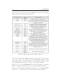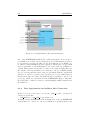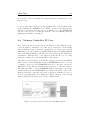
1
Master Thesis
Open Core Platform based on OpenRISC
Processor and DE2-70 Board
Xiang LI
Company:
ENEA
University:
Royal Institute of Technology,
School of Information and
Communication Technology,
Stockholm, Sweden
Industry Supervisor:
Johan Jörgensen
KTH Supervisor & Examiner: Ingo Sander
Master Thesis Number:
TRITA-ICT-EX-2011:62
This page is intentionally left blank
Abstract
The trend of IP core reuse has been accelerating for years because of the
increasing complexity in the System-on-Chip (SoC) designs. As a result,
many IP cores of different types have been produced. Meanwhile, similar to
the free software movement, an open core community has emerged because
some designers choose to share their IP cores by using open source licenses.
The open cores are growing fast due to their inherently attractive properties
like accessible internal structure and usually no cost for license.
Under this background, the master thesis was proposed by the company
ENEA (Malmö/Lund branch), Sweden. It intended to evaluate the qualities
of the open cores, as well as the difficulty and the feasibility of building an
embedded platform by exclusively using the open cores.
We contributed such an open core platform. It includes 5 open cores from the
OpenCores organization: OpenRISC OR1200 processor, CONMAX WISHBONE interconnection IP core, Memory Controller IP core, UART16550,
and General Purpose IOs (GPIO) IP core. More than that, we added the
supports to DM9000A and WM8731 ICs for Ethernet and Audio features.
On the software side, uC/OS-II RTOS and uC/TCP-IP stack have been
ported to the platform. The OpenRISC toolchain for software development
was tested. And a MP3 music player application has created to demonstrate
the system.
The open core platform is targeted to the Terasic’s DE2-70 board with
ALTERA Cyclone II FPGA. It aims to have high flexibility for a wide range
of embedded applications and at the same time with very low costs.
The design of the thesis project are fully open and available online. We hope
our work can be useful in the future as a starting point or a reference both
for academic research or for commercial purposes.
Keywords: SoC, OpenCores, OpenRISC, WISHBONE, DE-70, uC/OS-II
i
This page is intentionally left blank
Acknowledgement
This master thesis was started in January, 2008. It cost me and my partner
Lin Zuo more than 6 months to implement the project. There were lots of
difficulties when solving the technical issues, but the writing of the thesis was
even a greater challenge that I ever had. Finally the writing was completed
in January, 2011.
During the time, many people generously gave considerable help to me.
Without those supports the thesis wouldn’t have been come to this far.
So hereby I’d take the opportunity to express my deepest gratitude to the
following people:
Johan Jörgensen, the ENEA hardware team leader and our industry supervisor. Johan is the best supervisor that I can expect. He is knowledgeable,
experienced and full of brilliant ideas. He is good at communicating and encouraging people. With a short conversation he can take my pressures away.
As a supervisor, he participated almost in all aspects during the thesis. He
proposed the topic, made the detailed plan together with us, helped to setup
the working environment, and kept checking our progress. When we were in
trouble, he provided not only useful suggestions but sometimes even looked
down to the source code level. When I was upset because the thesis writing
went slow, he was always supportive. It is my pleasure to have Johan as a
supervisor.
Ingo Sander, our KTH supervisor and examiner. Ingo’s lectures were very
impressive and valuable to me, which opened many windows to the new
fields. This was the reason I wanted to be his thesis student. Ingo actively
monitored the thesis although we were in different cities. He followed our
weekly reports and replied with advice and guidance. He tried to set higher
requirements to us, which created bigger challenges but I also gained more
experiences at the same time. And I especially appreciate his patience when
the thesis writing was failed to finish on time. The knowledge learnt from
Ingo truly benefits me, which I am using it everyday now in my career life.
iii
iv
Lin Zuo, my thesis partner and good friend. As a partner he contributed
a solid part to the thesis. He worked really hard and took over many heavy
tasks. For some of them I was not confident but Lin made them come true. As
a friend he is a very funny guy. When our work seemed going to a dead end,
Lin can easily amuse me in his special way and ease the anxieties. Thanks to
him the thesis becomes a successful and interesting memory when we look
back to the life in Malmö.
And my parents. Without their love and supports throughout my life, I
would never get this chance to write a master thesis acknowledgement.
Sincerely thanks to all the people who helped me on the way to my today’s
achievements. Thank you all!
Contents
Abstract
i
Acknowledgement
iii
List of Figures
xi
List of Tables
xv
1 Introduction
1
1.1
Background and Motivation . . . . . . . . . . . . . . . . . . .
1
1.2
Thesis Objectives . . . . . . . . . . . . . . . . . . . . . . . . .
3
1.3
Chapter Overview . . . . . . . . . . . . . . . . . . . . . . . .
5
References . . . . . . . . . . . . . . . . . . . . . . . . . . . . . . . .
6
2 Open Cores in a Commercial Perspective
2.1
7
Basic Concepts . . . . . . . . . . . . . . . . . . . . . . . . . .
8
2.1.1
What is Open Core? . . . . . . . . . . . . . . . . . . .
8
2.1.2
Formal Definition of Open Source
. . . . . . . . . . .
8
2.1.3
Licenses Involved to Evaluate . . . . . . . . . . . . . .
9
2.1.4
GNU and FSF . . . . . . . . . . . . . . . . . . . . . .
9
2.1.5
Free Software 6= Free of Charge . . . . . . . . . . . . .
10
v
vi
2.2
BSD License
. . . . . . . . . . . . . . . . . . . . . . . . . . .
10
2.3
GNU Licenses . . . . . . . . . . . . . . . . . . . . . . . . . . .
13
2.3.1
GPL . . . . . . . . . . . . . . . . . . . . . . . . . . . .
13
2.3.2
LGPL . . . . . . . . . . . . . . . . . . . . . . . . . . .
15
2.3.3
Evaluations on the GNU Licenses . . . . . . . . . . . .
17
2.4
The Price for Freedom — Comments on the GNU Philosophy
19
2.5
Developing Open Cores or Not — How Open Source Products
could Benefit . . . . . . . . . . . . . . . . . . . . . . . . . . .
22
2.6
Utilizing Open Cores or Not — Pros and Cons . . . . . . . .
23
2.7
The Future of Open Cores . . . . . . . . . . . . . . . . . . . .
25
2.8
Conclusion . . . . . . . . . . . . . . . . . . . . . . . . . . . .
26
References . . . . . . . . . . . . . . . . . . . . . . . . . . . . . . . .
27
3 Platform Overview
31
3.1
DE2-70 Board . . . . . . . . . . . . . . . . . . . . . . . . . . .
32
3.2
Digital System with Open Cores . . . . . . . . . . . . . . . .
33
3.2.1
System Block Diagram . . . . . . . . . . . . . . . . . .
33
3.2.2
Summary of Addresses . . . . . . . . . . . . . . . . . .
35
Software Development and Operating System Layer . . . . .
36
3.3.1
Software Development . . . . . . . . . . . . . . . . . .
37
3.3.2
Operating System and uC/OS-II RTOS . . . . . . . .
41
3.3.3
uC/TCP-IP Protocol Stack . . . . . . . . . . . . . . .
42
3.3.4
Hardware Abstraction Layer (HAL) Library . . . . . .
42
3.4
Demo Application: A MP3 Music Player . . . . . . . . . . . .
43
3.5
Summary . . . . . . . . . . . . . . . . . . . . . . . . . . . . .
44
References . . . . . . . . . . . . . . . . . . . . . . . . . . . . . . . .
45
3.3
vii
4 OpenRISC 1200 Processor
47
4.1
Introduction . . . . . . . . . . . . . . . . . . . . . . . . . . . .
47
4.2
OR1200 Features and Architecture . . . . . . . . . . . . . . .
49
4.3
OR1200 Registers . . . . . . . . . . . . . . . . . . . . . . . . .
51
4.4
Interrupt Vectors . . . . . . . . . . . . . . . . . . . . . . . . .
53
4.5
Tick Timer (TT) . . . . . . . . . . . . . . . . . . . . . . . . .
55
4.6
Programmable Interrupt Controller (PIC) . . . . . . . . . . .
56
4.7
Porting uC/OS-II to OR1200 . . . . . . . . . . . . . . . . . .
58
4.7.1
Introduction . . . . . . . . . . . . . . . . . . . . . . .
58
4.7.2
uC/OS-II Context Switching . . . . . . . . . . . . . .
58
4.7.3
Context Switching in OR1200 Timer Interrupt . . . .
59
4.7.4
Summary . . . . . . . . . . . . . . . . . . . . . . . . .
61
References . . . . . . . . . . . . . . . . . . . . . . . . . . . . . . . .
61
5 WISHBONE Specification and CONMAX IP Core
63
5.1
Importance of Interconnection Standard . . . . . . . . . . . .
64
5.2
WISHBONE in a Nutshell . . . . . . . . . . . . . . . . . . . .
66
5.2.1
Overview . . . . . . . . . . . . . . . . . . . . . . . . .
67
5.2.2
WISHBONE Interface Signals . . . . . . . . . . . . . .
68
5.2.3
WISHBONE Bus Transactions . . . . . . . . . . . . .
72
5.2.3.1
Single Read/Write Transaction . . . . . . . .
73
5.2.3.2
Block Read/Write Transaction . . . . . . . .
76
5.2.3.3
Read-Modify-Write (RMW) Transaction . .
78
5.2.3.4
Burst Transaction . . . . . . . . . . . . . . .
79
CONMAX IP Core . . . . . . . . . . . . . . . . . . . . . . . .
89
5.3.1
89
5.3
Introduction . . . . . . . . . . . . . . . . . . . . . . .
viii
5.3.2
CONMAX Architecture . . . . . . . . . . . . . . . . .
90
5.3.3
Register File . . . . . . . . . . . . . . . . . . . . . . .
90
5.3.4
Parameters and Address Allocation . . . . . . . . . . .
91
5.3.5
Functional Notices . . . . . . . . . . . . . . . . . . . .
92
5.3.6
Arbitration . . . . . . . . . . . . . . . . . . . . . . . .
93
References . . . . . . . . . . . . . . . . . . . . . . . . . . . . . . . .
95
6 Memory Blocks and Peripherals
6.1
6.2
On-chip RAM and its Interface . . . . . . . . . . . . . . . . .
97
99
6.1.1
On-chip RAM Pros and Cons . . . . . . . . . . . . . . 100
6.1.2
ALTERA 1-Port RAM IP Core and its Parameters . . 100
6.1.3
Interface Logic to the WISHBONE bus . . . . . . . . 101
6.1.4
Data Organization and Address Line Connection . . . 102
6.1.5
Memory Alignment and Programming Tips . . . . . . 106
6.1.6
Miscellaneous . . . . . . . . . . . . . . . . . . . . . . . 108
Memory Controller IP Core . . . . . . . . . . . . . . . . . . . 109
6.2.1
Introduction and Highlights . . . . . . . . . . . . . . . 110
6.2.2
Hardware Configurations . . . . . . . . . . . . . . . . 112
6.2.2.1
Address Allocation . . . . . . . . . . . . . . . 112
6.2.2.2
Power-On Configuration (POC) . . . . . . . 114
6.2.2.3
Tri-state Bus . . . . . . . . . . . . . . . . . . 115
6.2.2.4
Miscellaneous SDRAM Configurations . . . . 116
6.2.2.5
Use Same Type of Devices on One Memory
Controller . . . . . . . . . . . . . . . . . . . . 116
6.2.3
Configurations for SSRAM and SDRAM . . . . . . . . 116
6.2.4
Performance Improvement by Burst Transactions . . . 118
ix
6.3
UART16550 IP Core . . . . . . . . . . . . . . . . . . . . . . . 120
6.4
GPIO IP Core . . . . . . . . . . . . . . . . . . . . . . . . . . 122
6.5
WM8731 Interface . . . . . . . . . . . . . . . . . . . . . . . . 123
6.5.1
Introduction . . . . . . . . . . . . . . . . . . . . . . . 123
6.5.2
Structure of the WM8731 Interface . . . . . . . . . . . 123
6.5.3
HDL Source Files and Software Programming . . . . . 125
6.6
DM9000A Interface . . . . . . . . . . . . . . . . . . . . . . . . 126
6.7
Summary . . . . . . . . . . . . . . . . . . . . . . . . . . . . . 126
References . . . . . . . . . . . . . . . . . . . . . . . . . . . . . . . . 127
7 Conclusion and Future Work
129
7.1
Conclusions . . . . . . . . . . . . . . . . . . . . . . . . . . . . 129
7.2
Future Works . . . . . . . . . . . . . . . . . . . . . . . . . . . 132
7.3
7.2.1
Improve and Optimize the Existing System . . . . . . 132
7.2.2
Extension and Research Topics . . . . . . . . . . . . . 132
What’s New Since 2008 . . . . . . . . . . . . . . . . . . . . . 133
References . . . . . . . . . . . . . . . . . . . . . . . . . . . . . . . . 134
A Thesis Announcement
135
A.1 Building a reconfigurable SoC
using open source IP . . . . . . . . . . . . . . . . . . . . . . . 135
A.2 Further information . . . . . . . . . . . . . . . . . . . . . . . 136
B A Step-by-Step Instruction to Repeat the Thesis Project 137
B.1 Hardware / Software Developing Environment . . . . . . . . . 137
B.1.1 DE2-70 Board . . . . . . . . . . . . . . . . . . . . . . 138
B.1.2 A RS232-to-USB Cable . . . . . . . . . . . . . . . . . 138
x
B.1.3 An Ethernet Cable . . . . . . . . . . . . . . . . . . . . 139
B.1.4 A Speaker or an Earphone . . . . . . . . . . . . . . . . 139
B.1.5 A PC . . . . . . . . . . . . . . . . . . . . . . . . . . . 139
B.1.6 Cygwin . . . . . . . . . . . . . . . . . . . . . . . . . . 139
B.1.7 OpenRISC Toolchain . . . . . . . . . . . . . . . . . . . 140
B.1.8 Quartus II . . . . . . . . . . . . . . . . . . . . . . . . . 140
B.1.9 The Thesis Archive File . . . . . . . . . . . . . . . . . 141
B.2 Step-by-Step Instructions . . . . . . . . . . . . . . . . . . . . 141
B.2.1 Quartus Project and Program FPGA . . . . . . . . . 141
B.2.2 Download Software Project by Bootloader . . . . . . . 143
B.2.3 Download Music Data and Play . . . . . . . . . . . . . 147
References . . . . . . . . . . . . . . . . . . . . . . . . . . . . . . . . 151
List of Figures
2.1
Difference between LGPL and GPL . . . . . . . . . . . . . . .
17
2.2
Difference between open software and open core . . . . . . . .
18
2.3
Increasing competitors force the price lower . . . . . . . . . .
21
3.1
Platform overview . . . . . . . . . . . . . . . . . . . . . . . .
31
3.2
DE2-70 board . . . . . . . . . . . . . . . . . . . . . . . . . . .
32
3.3
Hardware block diagram of the DE2-70 . . . . . . . . . . . .
33
3.4
Open core system block diagram . . . . . . . . . . . . . . . .
34
3.5
Software development workflow . . . . . . . . . . . . . . . . .
38
4.1
OR1200 architecture . . . . . . . . . . . . . . . . . . . . . . .
50
4.2
Improve performance with Harvard architecture . . . . . . . .
50
4.3
16-bit SPR address format . . . . . . . . . . . . . . . . . . . .
53
4.4
Tick timer structure and registers . . . . . . . . . . . . . . . .
56
4.5
PIC structure . . . . . . . . . . . . . . . . . . . . . . . . . . .
57
5.1
Interconnection is important in multiprocessor systems . . . .
65
5.2
Overview of the WISHBONE . . . . . . . . . . . . . . . . . .
68
5.3
An example of WISHBONE signal connections . . . . . . . .
73
5.4
An example of WISHBONE single transactions . . . . . . . .
74
xi
xii
5.5
An example of a WISHBONE block write transaction . . . .
76
5.6
Block transactions are helpful in multi-master systems . . . .
77
5.7
Master B is blocked by master A . . . . . . . . . . . . . . . .
77
5.8
An example of a WISHBONE RMW transaction . . . . . . .
78
5.9
Maximum throughput with single transactions . . . . . . . .
79
5.10 Maximum throughput with burst transactions . . . . . . . . .
80
5.11 An example of a constant writing burst transaction . . . . . .
81
5.12 An example of an incrementing reading burst transaction . .
83
5.13 An burst transaction with wait states . . . . . . . . . . . . .
87
5.14 Core architecture overview . . . . . . . . . . . . . . . . . . . .
90
5.15 An example of using CONMAX . . . . . . . . . . . . . . . . .
92
6.1
Hardware platform architecture . . . . . . . . . . . . . . . . .
97
6.2
On-chip RAM module internal structure . . . . . . . . . . . . 102
6.3
Overview of data organization in OpenRISC systems . . . . . 105
6.4
Legal and illegal memory accesses . . . . . . . . . . . . . . . . 106
6.5
Example of memory padding . . . . . . . . . . . . . . . . . . 108
6.6
Memory Controller in the OpenRISC system . . . . . . . . . 109
6.7
Logic to activate a CS . . . . . . . . . . . . . . . . . . . . . . 113
6.8
32-bit address configuration for Memory Controller . . . . . . 114
6.9
WM8731 Interface in the OpenRISC system . . . . . . . . . . 123
6.10 WM8731 Interface internal structure . . . . . . . . . . . . . . 124
6.11 32-bit music data format . . . . . . . . . . . . . . . . . . . . . 126
B.1 Top level entity of the project . . . . . . . . . . . . . . . . . . 142
B.2 Program ALTERA FPGA . . . . . . . . . . . . . . . . . . . . 143
xiii
B.3 Software project . . . . . . . . . . . . . . . . . . . . . . . . . 144
B.4 Makefile script . . . . . . . . . . . . . . . . . . . . . . . . . . 145
B.5 Build software project . . . . . . . . . . . . . . . . . . . . . . 145
B.6 Check USB-to-serial port ID . . . . . . . . . . . . . . . . . . . 146
B.7 Downloading and flushing finished . . . . . . . . . . . . . . . 147
B.8 IP configuration
. . . . . . . . . . . . . . . . . . . . . . . . . 148
B.9 Start software project via bootloader . . . . . . . . . . . . . . 149
B.10 Ethernet connected . . . . . . . . . . . . . . . . . . . . . . . . 149
B.11 Decode MP3 file . . . . . . . . . . . . . . . . . . . . . . . . . 150
B.12 Set volume and play the music . . . . . . . . . . . . . . . . . 151
This page is intentionally left blank
List of Tables
3.1
Summary of addresses . . . . . . . . . . . . . . . . . . . . . .
36
4.1
OR1200 GPRs (part) . . . . . . . . . . . . . . . . . . . . . . .
52
4.2
Exception types and causal conditions . . . . . . . . . . . . .
54
6.1
Parameters of 1-port RAM IP core . . . . . . . . . . . . . . . 101
6.2
Data organization for 32-bit ports
6.3
Memory Controller register configurations . . . . . . . . . . . 118
6.4
System performance test results . . . . . . . . . . . . . . . . . 119
6.5
NIOS II processor comparison (part) . . . . . . . . . . . . . . 120
6.6
List of memory blocks and peripherals . . . . . . . . . . . . . 126
. . . . . . . . . . . . . . . 103
xv
This page is intentionally left blank
Chapter 1
Introduction
This chapter intends to give an introduction and a chapter overview to the
master thesis made by Xiang Li and Lin Zuo.
1.1
Background and Motivation
The goal of the thesis is to implement a low cost computing platform by
exclusively using open source Intellectual Property (IP) cores.
The idea was brought by Johan Jörgensen, the hardware team leader from
ENEA [1]. We have discussed the reasons to start this project, which are
listed below:
• ENEA wants to gain knowledge and insight in the viability of using
open cores.
• Based on the knowledge they can decide whether or not to start business involving HW design (ASIC/FPGA soft/hard IP cores).
• If the platform is successful, it might be continued and improved as a
product.
• This project also proves some embedded applications can be done with
the open cores.
3 factors of the recent development and innovation of the System-on-Chip
(SoC) technology give the possibility to do this thesis:
1
2
CHAPTER 1
1. The Design Reuse methodology with IP cores
As the increasing complexity of the digital electronic systems and the
growing time-to-market pressure, engineers are forced to utilize previously made blocks, i.e. IP cores, as many as possible into new designs.
This is called design reuse methodology.
The methodology produces more and more IP cores that are ready
to use. These IP cores provide great convenience when designing new
systems. For example in this thesis project we can quickly build a
system with the selected IP cores. If we had to create those IP cores
ourselves, it would be an impossible work for us to finish the system
within limited time.
2. The appearance of the Open Core community
Most IP cores are implemented by Hardware Description Languages
(HDLs), either VHDL or Verilog HDL. The HDL source codes can be
further synthesized to digital circuits by software tools.
Similarly to the free software community, there has emerged an open
core community, where the designers publish their IP core HDL source
codes that are protected by open source licenses. The open source IP
cores are called in short Open Cores.
The OpenCores organization is the world’s largest site/community for
development/discussion of open source hardware IPs [2, 3]. In the website, there are hundreds of opening or finished projects regarding to the
open cores, which cover from CPUs to all kinds of peripherals. Some of
the open cores are with very good quality and have been successfully
used in commercial/industrial projects.
One of the most interesting advantages of the open cores is they are
free to access. This is especially critical for thesis students like us who
do not have enough budgets to acquire commercial IP cores. Besides,
build up a low cost system with open cores for commercial purposes
is also an attractive topic.
3. The fast system prototyping via FPGA development board
Compare to the traditional ASIC design flow which takes long time
and is also more costly/risky, the fast system prototyping on a FPGAbased development board has proven a good methodology to accelerate
the functional verification. Many vendors have designed a large number
of FPGA boards for this purpose with high performance. One example
is the Terasic’s DE2-70 board [4, 5] that we used for the thesis project.
The DE2-70 is equipped with a high density ALTERA Cyclone II
FPGA, large volume RAM/ROM components, and plenty of peripherals including Audio devices and Ethernet interface. It provided us
CHAPTER 1
3
an ideal hardware platform to try out open cores, and allowed us to
quickly build up an open core based digital system with demonstrations.
Because of the 3 factors described above, it becomes feasible to execute
the project, which implements an open core based computing system on
a DE2-70 FPGA board which is low cost but powerful and versatile. If
such a system can be made, it would be interesting both for commercial
and academic purposes. With the platform, many other possibilities can be
further extended.
As mentioned before, the idea was initially proposed by Johan Jörgensen
from ENEA and who is the industrial supervisor of us. The thesis is also
coached by Ingo Sander, our supervisor from KTH.
The thesis was performed by Xiang Li (me) and my partner Lin Zuo in
ENEA (Malmö/Lund) branch, Sweden. Most of the implementation was
done from January to July in 2008. Because of the administrative reasons
we had to write 2 separate theses, which have similar structures but different
focuses based on our responsibility. For Lin Zuo’s thesis, please refer to [6].
The theses and the archived project files are available at this link [7].
1.2
Thesis Objectives
The thesis is to implement a computing platform with open cores. However
this is a very broad topic. After discussed and approved by the supervisors,
we had elaborated and refined the thesis into detailed tasks. In this section
the tasks of the thesis are summarized, including both we achieved and failed
due to the time limitation.
The original thesis announcement made by Johan Jörgensen is copied as
Appendix A, from where we can get an overall idea of the initial purposes
of the thesis:
1. Evaluate quality, difficulty of use and the feasibility of open source IPs
2. Design the system in a FPGA and also evaluate the system performance
3. Investigate license issues and their impact on commercial use of open
source IP
4. Port embedded Linux to the system
4
CHAPTER 1
Because it was hard to foresee how much work can be completed within
limited time, after discussion we defined the thesis tasks in 3 different levels:
Level One/Two/Three.
Below it is the list of the tasks. The responsibility is marked in the brackets.
The Level One tasks are mandatory for the thesis. It contains the very basic
goals to create a working system with open cores:
• Study the open source licenses and investigate the impacts of the licenses for commercial usages (Xiang and Lin)
• Build a FPGA system on a DE2-70 develop board with the following
open cores:
– OpenRISC CPU (Xiang)
– WISHBONE bus protocol and CONMAX IP core (Lin)
– Memory Controller for SSRAM/SDRAM (Lin)
– UART connection (Xiang)
• Setup the toolchain (compiler etc.) for software development, and design applications for demonstrating the hardware platform (Xiang)
• Port uC/OS-II Real Time Operating System (RTOS) to the platform
(Xiang)
• Build an equivalent system with ALTERA technology and evaluate
the performance comparing to our system (Lin)
The Level Two tasks are mainly to extend the system with more features:
• Add support to WM8731 Audio CODEC such that the system can
play music (Xiang)
• Add support to DM9000A Ethernet controller (Lin)
• Port uC/TCP-IP stack to the system such that the system can communicate with a PC with TCP/UDP protocols (Lin)
• Design a software application to demonstrate these features (Xiang)
The Level Three tasks are advanced tasks:
• Build multiprocessor system with more than one OpenRISC CPU
CHAPTER 1
5
• Port Linux to the platform
At the end, we finished most tasks on Level One and Two, but failed to
start the tasks of Level Three because of the limited time of the thesis.
1.3
Chapter Overview
The thesis contains 7 chapters. An overview of the chapters is given below.
As mentioned before, the contents of this thesis focuses mainly on the tasks
that Xiang Li was responsible. For Lin Zuo’s part, e.g. system performance
comparison, please refer to Lin’s thesis [6].
Chapter 1 is the chapter you are reading which gives an introduction to
the thesis.
Chapter 2 introduces 3 widely used open sources licenses: GPL, LGPL and
the BSD license, and discusses the impacts of the licenses for the open cores.
The chapter is placed before the system implementation chapters because
it is a primary task to investigate. We don’t want to violate the licenses
while using open cores. Also it would be interesting to know the influences
of the open sources licenses if an open core based system will be used for
commercial purposes.
From Chapter 3 to Chapter 6, the implementation of the open core based
computing platform is described.
Chapter 3 gives an overall impression of the system architecture, including
the hardware block diagram, the software development workflow, and the
description of a demonstration application.
Chapter 4 focuses on the OpenRISC OR1200 CPU, which is the heart of
the computing system. The processor is discussed from many aspects like
hardware, software, and porting the uC/OS-II RTOS.
Chapter 5 is dedicated for the WISHBONE bus protocol and an open core
implementation of the protocol, i.e. the CONMAX IP core. The bus protocol
organizes the whole system. It is so important that we will use a separate
chapter for it.
In Chapter 6 the memory blocks and the peripherals of the system are
introduced, including Memory Controller IP core, UART 16550 IP core,
GPIO IP core, and the interfaces for WM8731 and DM9000A etc.
6
CHAPTER 1
Chapter 7 finally concludes the thesis, and also provides a list of todo
which can be interesting topics to research in the future.
At the end, 2 appendixes are attached. Appendix A is the copy of the
thesis announcement made by Johan Jörgensen. Appendix B is a step by
step instruction of how to reproduce the project on a DE2-70 board with
the downloaded files from [7].
References:
[1] Website, ENEA, http://www.enea.com/, Last visit: 2011.01.31,
Enea is a global software and services company focused on solutions for
communication-driven products.
[2] Website, OpenCores.org, http://www.opencores.org/,
Last visit: 2011.01.31,
OpenCores is a community that enable engineers to develop open source
hardware, with a similar ethos to the free software movement.
[3] Webpage, Advertising at OpenCores, from OpenCores.org,
http://opencores.org/opencores,advertise, Last visit: 2011.01.31.
[4] Website, Terasic Technologies, http://www.terasic.com.tw/,
Last visit: 2011.01.31.
[5] Webpage, Altera DE2-70 Board, from Terasic Technologies,
http://www.terasic.com.tw/cgi-bin/page/archive.pl?Language=
English&No=226,
Last visit: 2011.01.31.
[6] Lin Zuo, System-on-Chip design with Open Cores, Master Thesis,
Royal Institue of Technology (KTH), ENEA, Sweden, 2008,
Document Number: KTH/ICT/ECS-2008-112.
[7] Webpage, The online page of the thesis and project archive,
http://www.olivercamel.com/post/master thesis.html,
Last visit: 2011.01.31.
Chapter 2
Open Cores in a Commercial
Perspective
This chapter might look a bit weird in an engineering thesis, but it was
really the very primary task to do even before the implementation of the
thesis started.
Because the thesis involves open cores and most open cores are covered by
various open source licenses, like GPL, LGPL and the BSD license, good
understanding to those licenses are inevitably needed when evaluating open
cores. Quoted Johan Jörgensen, our thesis supervisor, “We want a platform
that is reconfigurable, no-frills and cheap that can be used for in-house
projects, but we do not want to hit the mines of open source. So we need
to know if open cores are a safe bet and what kind of performance they will
have on a given FPGA.” In this chapter, 3 of most widely used open source
licenses, GPL, LGPL and the BSD license are introduced.
If building an open core based system really become true, another topic
is also interesting for the companies: would the open source licenses limit
the system for commercial purposes? What are the benefits and the tradeoffs? As the thesis project was executed in the company ENEA, we believe
analyses about the open cores in a commercial perspective would be useful
for them. So some general discussions are also made in the chapter about
utilizing open cores on behalf of a company.
Hope the introductions and evaluations to the open cores and the open
source licenses in this chapter could answer 2 questions: As a company
project manager, should we develop new open cores? Or should we improve
existing open cores and integrate them into the next products?
7
8
2.1
CHAPTER 2
Basic Concepts
In this section several basic concepts regarding to open cores are introduced.
2.1.1
What is Open Core?
Open core is a shortening of Open Source Intellectual Property (IP) Core,
which is a combination of the concepts of “open source” and “IP core”.
There is no need to spend much words on introducing IP cores because
those are quite well known and discussed already in plenty of articles like
[1, 2]. In short, the increasing complexity of electronic systems and time-tomarket pressure force engineers to utilize already made blocks, i.e. IP cores,
as many as possible into the next system, which is so called the design reuse
methodology.
Actually semiconductor IP cores have a broad definition and can be in any
form of “reusable unit of logic, cell, or chip layout design” [3], but in this
thesis, the discussion of the “IP Core” is narrowed down to only digital logic
blocks designed by HDL and targeted to FPGA/ASIC. This is because all
open cores used in the thesis project are of this type.
2.1.2
Formal Definition of Open Source
When coming to the other concept “open source” of the open core, most
people simply just take it literally as “you can look at or get a copy of
source code”. However, this is a common misunderstanding.
Open Source Initiative (OSI) [4], an official organization of open source
community, has a formal definition to the term “open source”, which can be
found on the Internet at the link [5]. It is too long to cite the full texts here.
If haven’t read the concept before, you will find the open source is a more
complicated concept than ever imagine. It does not only refer to the access
to source codes, but also defines lots of criteria needed to follow. The actual
effects of those criteria might be important to be aware of, before publish
products as open source or utilize something in any form of open source,
which naturally includes open cores.
Because the OSI definition of open source is too long, personally in the thesis
I would like to simplify the definition to “the source codes that are covered
by certain open source licenses”, such that we can concentrate on studying
CHAPTER 2
9
the open source licenses only.
A list of approved open source licenses can be found in OSI’s website [6].
Different licenses in the list may have different rules and regulations, but
if the source codes are covered by any one of them, you may call it open
source.
2.1.3
Licenses Involved to Evaluate
Now we have established the open source licenses as the target to study.
Next question is to define what licenses are involved. Because the OSI list
of licenses is really long, not possible to go through them all.
All open cores used in the thesis project are covered by either LGPL or the
BSD license. Due to the LGPL is based on the GPL, all 3 licenses, i.e. GPL,
LGPL and the BSD License, will be introduced in the later sections.
Actually the open cores used in the thesis are not covered by the exact BSD
license, but a “BSD-style” license. However the introduction to the original
BSD license will still be useful.
2.1.4
GNU and FSF
Because the GPL and LGPL will be introduced later, several words related
to the background are worth to mention.
The letter “G” in the GPL and LGPL stands for “GNU”, which is a name of
a project to develop a Unix-like operating system that is completely free software. The GNU licenses were initially designed to protect the liberty of the
free software of that project without being violated. But later they became
more and more popular and now widely used to cover a large proportion of
free software all over the world.
Sometimes the GNU is also treated incorrectly as an organization that
is responsible for the project, probably because its website is named as
www.gnu.org. But in fact it is Free Software Foundation (FSF) that takes
the role. The FSF is a corporation founded to support the free software
movement as well as to be a sponsor to the GNU project. So don’t be confused when seeing “Copyright (c) <year>, Free Software Foundation, Inc”
in the GNU licenses.
Both the GNU project and the FSF were started by Richard Stallman, a
legend because of his contributions for the free software movement. The
10
CHAPTER 2
thesis won’t go further on his story, but lists some references instead [7–14].
2.1.5
Free Software 6= Free of Charge
The free software movement mentioned above is a social movement aiming
to prompt people’s freedom on accessing and improving the source codes of
the software. If a software truly assures the freedom for the users, it can be
called free software.
Free software is a concept close to the open source but highlights more on the
rights of the freedom [15]. Similarly, it is also often misunderstood literally as
“the software that is free of charge”. We will come back again to this concept
in the later section, for now please just remember the official explanation
to the concept here: “ ‘Free software’ is a matter of liberty, not price. To
understand the concept, you should think the ‘free’ as in ‘free speech’, not
as in ‘free beer’ ” [16].
The explanation is meaningful. It implies people can sell free software with
a price, in case of the freedom is guaranteed as the same time. It is allowed
to make profits by utilizing free software, so as to the open cores.
So far, all related concepts have been introduced. From the next section, we
will start discussing about the open source licenses, and then make analyses
for the open cores in a commercial perspective.
2.2
BSD License
The Berkeley Software Distribution (BSD) license gets its name because
it was first designed to cover a Unix-like operating system developed by
University of California, Berkeley [17]. Later it was revised by removing
a clause which was too impracticable and limited the license to be widely
accepted. This story can be found in [17, 18]. Now the BSD license is also
called the “new” BSD license1 .
The BSD license is the 3rd most popular open source license according to the
article [19], which also mentions that the first two ahead of it are the GPL
and the LGPL, and those two account for almost 80% of all open source
licenses in use. The article doesn’t tell how the statistics were made, but it
shows the truth that the 3 licenses are quite widely used in the open source
world.
1
Or modified, or simplified, or 3-clause BSD license
CHAPTER 2
11
The BSD license is popular probably because it has very few restrictions,
both for authors and especially for users. The full text of the BSD license
can be found at [20].
Let’s take a look at the 3 clauses of the license:
Redistribution and use in source and binary forms, with or without modification, are permitted provided that the following conditions are met:
• Redistributions of source code must retain the above copyright notice,
this list of conditions and the following disclaimer.
• Redistributions in binary form must reproduce the above copyright
notice, this list of conditions and the following disclaimer in the documentation and/or other materials provided with the distribution.
• Neither the name of the <ORGANIZATION> nor the names of its
contributors may be used to endorse or promote products derived from
this software without specific prior written permission.
The 3 clauses assert only minimum requirements comparing to the other
open source licenses.
If we try to understand the clauses, Clause 1 means people cannot remove
the text of the BSD license from the source codes. Clause 2 says if someone
will redistribute the source codes in another format, like selling a software
product, the people has to announce that the product contains something
covered by the BSD license designed by someone else. Both Clause 1 and 2
are very basic things that everyone should do by conscience, even if there are
not asked by a license. Just like when writing an article, a list of references
is needed to acknowledge previous contributors’ work.
Clause 3 is a little complicated to understand. It is used to prevent the original author’s name of the source codes from being abused, and the drawbacks
of the source codes from being incorrectly attributed. For an example, if
someone gets some BSD license protected source codes which were made by
a famous expert, the people can improve the codes and redistribute/sell it,
but cannot use the expert’s name in the advertisement without permission.
Under the 3 clauses, there is a long paragraph of disclaimer in the BSD
license. According to it, basically the source codes covered by the BSD license
provide no warranties to the users. This is good for the authors since they
promise nothing through the license. And this is fair because most authors
give the source codes for free when they choose the BSD license, so of course
they should not be responsible for any liability. But for the users, they may
take risks when working with the source codes under the BSD license.
12
CHAPTER 2
Now let’s evaluate the BSD license in a business world.
First of all, the license talks nothing regarding to money. This means technically people can develop source codes under the BSD license and sell it at
any price he/she wants, although this is not a usual case. Because if someone
would like to make money by selling products, he/she would rather choose
a commercial license stricter than the BSD license which prohibits making
copies freely.
Another interesting point is that the BSD license sets no limitations on
keep using the license after redistributing. This is different from the GNU
licenses. If the open source codes are there, everyone can take the codes,
modify, improve and redistribute them. The BSD license requires nothing
on what license to use for the modified versions. So it is totally possible
to use another commercial license over the BSD license. This is very good
news for vendors, because they can take a BSD licensed IP core, integrate
it into a new product, and then sell it as the way they want with their own
commercial licenses.
For the open cores, perhaps the most attractive part of the BSD license is
that it doesn’t ask you to publish the modified source codes when redistribute (or sell) the products in a non-source form. On the contrary, the
GNU licenses do. Thinking about the open cores which are in the form of
the HDL source codes, after the products are finally built and ready to sell,
the open cores will not be in the HDL codes any more but become silicon
chips. Because the BSD license doesn’t force to provide source codes, the
companies can safely make modifications to the BSD licensed open cores,
combine them together with their own patents, meanwhile happily selling
the new chips without telling their competitors the design details.
To conclude the BSD license, it is a quite loosely restricted open source license. Modified source codes that originally covered by the BSD license even
do not have to be open source any more. This makes the license completely
compatible for commercial purposes. Companies are welcome to utilize open
cores under the BSD license in their business, using their own commercial
licenses instead, as long as keeping a reference together with the products
which shows certain BSD licensed open cores are contained, like including a
copy of the license in the user manuals.
CHAPTER 2
2.3
13
GNU Licenses
In this section we are about to introduce the GNU licenses, including the
GPL and LGPL.
GNU General Public License (GPL) is one of the most popular open source
licenses and perhaps the strictest of the world published by the FSF. GNU
Lesser General Public License (LGPL) is a supplement of additional permissions to the GPL by removing some limitations from it. So to speak, the
LGPL is based on the GPL rather than an individual license. We will start
with the GPL and then take a look at how the LGPL is lesser than the GPL.
2.3.1
GPL
The GPL is a very strict open source license that designed to make the
source codes become free software and keep them as free software forever.
The full text of the GPL can be found at [21].
According to the formal definition of “free software” [16], a program is free
software if its users have all 4 freedoms:
• The freedom to run the program, for any purpose;
• The freedom to study how the program works, and adapt it to your
needs;
• The freedom to redistribute copies so you can help your neighbor;
• The freedom to improve the program, and release your improvements
to the public, so that the whole community benefits.
So generally, if someone is using source codes covered by the GPL, he/she has
the rights to “run, copy, distribute, study, change and improve the software”
[16]. On the other hand, if someone decides to use the GPL to cover the
designed programs when publishing them, he/she grants these rights to the
future users and customers.
To make sure the freedom is guaranteed for all GPL users and all potential
users in the future, the license designer also defined obligations that the
GPL users must follow while enjoy the freedom.
14
CHAPTER 2
There are 4 main obligations can be summarized among the long text of the
GPL:
1. Keep using the GPL forever;
2. Provide source codes in any case;
3. Publish the modified parts;
4. Make the GPL cover the entire new project.
First and foremost, the GPL will keep covering the source codes forever, and
there is no way to remove or bypass it since it is applied. If people decide to
edit GPLed source codes and redistribute them, the GPL will be the only
choice as the license for the revised work. The people cannot use any other
alternative license to cover the new work instead of the GPL, because “This
License gives no permission to license the work in any other way . . . ” (GPL
section 5). There are many licenses that have no conflicts with the GPL
in principle, like the BSD license. This is called “GPL compatible”. People
can create a new project by combining 2 separate works that the one is
covered by the BSD license and the other by the GPL without any problem.
However, only the GPL can be used to cover the new project, not the BSD
license. So once the GPL is there, it will be always there. It is required to
keep using the license forever for all improved versions in the future.
The 2nd obligation well expresses the thought of the GPL as an open source
license—the source codes have to be provided in any case. After modify a
GPLed work and when redistributing it, if the final product is in the form of
the source codes, it is easy to understand that the codes should be open. But
even if the final product is in a non-source form, according the section 6 of
the GPL, the source codes that generating the final product still have to be
provided with the products. For example, if a company produces and sells
GPLed software in non-source form like binary or executable files, normally
it has to provide either an extra CD including the source codes or a web
server which allows the users to download those files freely. This obligation
makes the GPL stronger than many other open source licenses like the BSD
license, which do not ask for a copy of the source codes. When coming to
hardware world for the open cores, this means at the same time silicon chips
are sold, certain HDL source codes and/or design details have to be public.
The 3rd obligation makes the GPL even stronger. It forces its users to publish
also the modified parts when providing the source codes, i.e. it is a must to
show ALL source codes which generating the final products. For example, if
someone started with a GPLed work and spent a lot of time to improve it,
when selling improved version he/she cannot just provide the original source
CHAPTER 2
15
codes without the details of the modifications. According to the GPL, no
secret is allowed to hide. All details of the modifications and improvements
have to be public, although not everyone might be happy to do so.
Most disagreements and arguments come from the last obligation, that the
GPL must cover the entire project, which already caused many criticisms
[22, 23]. In section 0 the GPL defines the term “modify”. It says “To ‘modify’
a work means to copy from or adapt all or part of the work in a fashion
requiring copyright permission, other than the making of an exact copy.”
And when “Conveying Modified Source Versions”, in section 5 term (c) the
GPL makes the rules: “You must license the entire work, as a whole, under
this License to anyone who comes into possession of a copy. This License will
therefore apply, . . . , to the whole of the work, and all its parts, regardless
of how they are packaged. This License gives no permission of license the
work in any other way . . . ” These clauses make the GPL spread to the parts
which previously could have not belonged to a GPL covered work. And this
is why some people called the GPL “infectious”. When we are going to reuse
some GPLed source codes for a new product, this will surely fall into the
definition “modify”. And when redistributing the improved version, section
5 will take effect to force applying the GPL to the whole new work, which
means we have to unfortunately open source for the entire work, including
the parts which are not initially covered by the GPL. For a simple example, if
a program which had 4,950 lines of codes and now adding a 50 lines function
copied from a GPLed software, all the final 5,000 lines have to become open
source and be public to the future users, even though the GPLed codes only
counts 1% of all.
2.3.2
LGPL
The last obligation of the GPL described in last section is obviously too
strong than many users who are not that enthusiastic in free software movement could accept. Indeed, many companies are afraid that their patents
and proprietaries could be violated when combing them with GPLed things,
so they keep themselves away from the GPL. Therefore, a light version of
the GPL is developed by the FSF by removing the infectious attribute from
the GPL.
The LGPL is previously named as “GNU Library General Public License”,
which shows it is primarily developed for libraries. Because the GPL is too
strict and infectious, if it is applied to a library, all programs that linking to
this library will have to become open source. This is not the case that many
developers, especially commercial companies, would like to see. And as a
result, the GPLed library may be gradually forgotten by people. To solve
16
CHAPTER 2
the problem, a compromised license, i.e. the LGPL, is designed and used
particularly for libraries. Soon, the FSF realized that (1) LGPL can be used
for not only libraries but many other software as well, and (2) the choosing
between the GPL and the LGPL by authors is a strategy of development
[24], but not only depend on whether it is targeted to a library or not, so
now the LGPL is renamed to “GNU Lesser General Public License”.
The LGPL is a set of additional permissions added to the GPL. By those
permissions, the LGPL removes the last obligation of the four described
above. And this is the only difference between the LGPL and the GPL. All
the other three obligations of the GPL still remain.
In section 0, LGPL defines several more terms than the GPL:
“The Library” refers to a covered work governed by this License, other than
an Application or a Combined Work as defined below.
An “Application” is any work that makes use of an interface provided by
the Library, but which is not otherwise based on the Library.
A “Combined Work” is a work produced by combining or linking an Application with the Library.
In section 4 “Combined Works” the LGPL says:
You may convey a Combined Work under terms of your choice that, taken together, effectively do not restrict modification of the portions of the Library
contained in the Combined Work and reverse engineering for debugging such
modifications . . .
And in section 5 “Combined Libraries” it says:
You may place library facilities that are a work based on the Library side
by side in a single library together with other library facilities that are
not Applications and are not covered by this License, and convey such a
combined library under terms of your choice . . .
By these clauses, the LGPL clearly separates 2 different sets of components,
the “Library” that is a LGPLed module and an “Application” from somewhere else which isn’t governed by the license. Because the LGPL is initially
designed for libraries, it keeps using the phrases like library and application.
According to the LGPL, it will not affect other modules which just connect
to a LGPLed module. We can draw a picture to explain the rules. Suppose
we have a software project including 2 existed libraries and a lately designed
application linked to them. As Figure 2.1 (a) shows, Library A is covered by
the LGPL, while Library B is from a company and covered by a commercial
license. The Application links to the 2 libraries. In this case, the whole
CHAPTER 2
17
project is a combined work, and it is allowed to license the project under
user defined terms, as long as these terms do not conflict with the LGPL,
and also guarantee that the LGPLed library is still open source.
(a) LGPL stays along with other licenses
(b) GPL infects other modules
Figure 2.1: Difference between LGPL and GPL
However, the scenario will be totally different if Library A is covered by the
GPL. If it is, because the GPL forces the whole project to be licensed only in
the way of the GPL, all the rest parts of the project, i.e. the Library B and
the Application, have to become GPLed whatever their previous licenses
are.
2.3.3
Evaluations on the GNU Licenses
So far, the introduction to the GPL and the LGPL is finished. It is time
to go back to our topic to discuss how the open cores will be influenced by
these licenses.
For commercial purposes, my answer is that: generally the open cores that
covered by the LGPL are OK to use if the company won’t spend too many
efforts to improve the cores; while the GPLed open cores are not suggested
for commercial purposes, unless they are used individually per silicon chip.
Basically the open cores covered by the LGPL are free to use is because they
are not infectious like the GPL. So there is no worry when connecting the
open cores and the proprietary IP cores together to compose a larger system.
Besides, most likely the utilized open cores will not be modified too much
than the initial version. Otherwise companies would rather like to invent a
new core than reusing an existing one. So this means to open source for the
details of the improved parts as required by the LGPL would be acceptable
for the companies.
18
CHAPTER 2
Because of 2 reasons the companies need to be careful when facing to the
GPLed open cores: (1) the GPL is infectious, and (2) the difference between
open source software and open cores.
For software, the GPL defines a concept called “aggregate” in section 5:
A compilation of a covered work with other separate and independent works,
which are not by their nature extensions of the covered work, and which are
not combined with it such as to form a larger program, in or on a volume
of a storage or distribution medium, is called an “aggregate” . . . Inclusion of
a covered work in an aggregate does not cause this License to apply to the
other parts of the aggregate.
By this definition, the GPL won’t infect if any 2 programs just stay together
and are not related to each other. For example, if a web browser and a media
player are stored in the same computer, the media player license will not
influence the web browser if it is using the GPL. Or another example, if a
compiler is GPLed, the source codes being processed by the compiler do not
have to be open source.
Unfortunately, the concept of aggregate doesn’t work for open cores in the
hardware world. Although open software and open cores are both in the form
of source codes at the beginning, open software will be finally compiled into
binary or executable format which is still software, however the HDL codes
of open cores will be synthesized by EDA tools and transformed to hardware
at the end. Like Figure 2.2 shows, in a hardware system, every open core
will be connected together via a bus or other interconnection structures. As
a result, the definition of aggregate is no longer satisfied in this case, and
the GPL will be applied to the whole system.
(a) Software aren’t linked in computers
(b) IP cores link with others in chips
Figure 2.2: Difference between open software and open core
So to speak, GPLed open cores are not suggested to use because it will force
other parts of system to become open source, which is generally the case that
CHAPTER 2
19
companies would not like to see. There are indeed some really good open
cores under the GPL like the LEON processor with SPARC architecture
[25], but unless they are used solely to form a system, i.e. to make a silicon
chip includes only one open core so that no other cores will be infected, open
cores covered by the LGPL will be always a better choice than the GPL.
To sum up this section, both the GPL and the LGPL are very strict open
source licenses. They grant users the freedom to use source codes, but meanwhile stipulate obligations must to follow. Generally, the open cores under
the LGPL have no problem for commercial purposes, but the GPLed open
cores are not because they are infectious. When the products including open
cores under the LGPL are published, basically a company has to do the following:
1. Announce the open cores contained in the product;
2. Attach a copy of both the GPL and the LGPL;
3. Publish the source codes that generating the final product.
2.4
The Price for Freedom — Comments on the
GNU Philosophy
The GNU GPL and LGPL have been introduced in the previous section. Now
it is time to think about something at a higher level—the GNU philosophy
we could learn from the licenses. Let’s start from a misunderstanding of the
free software.
Many people misunderstand the word “free” of “free software” as “free of
charge” or “zero price”. So they feel strange and uncomfortable when they
are asked to pay for the copies of the free software (like some Linux products)
from distributors. They may query “Isn’t this FREE software?”
Actually this is a common misunderstanding for free software. In dictionary
there are 2 meanings of the word “free”. The one is “not under control or
not subject to obligations”, i.e. freedom, and the other is “available without
charge”, i.e. no cost for money. The GNU says clearly in the 3rd paragraph
of the preamble of the GPL text as “When we speak of free software, we are
referring to freedom, not price.” They also emphasize this point many times
by saying “Free software is a matter of liberty, not price. To understand
the concept, you should think of free as in free speech, not as in free beer.”
[15, 16, 26] In fact, the GNU even encourages people to charge as much
money as they can by selling free software [26].
20
CHAPTER 2
From which we can feel at the same time the GNU is struggling on protecting
the freedom of knowledge accessibility, they are also trying to clarify that
the free software licenses won’t prevent people from making money. So on
one hand the GNU believe the knowledge should be the wealth of all human
beings and no one should set barriers to limit its propagations, such that
people could benefit from the knowledge. On the other hand, they hope the
businessmen can charge at any price as they want to get a substantial profit
by selling free software as long as they follow the licenses and promise no
restriction on the freedom.
This sounds great, like a win-win solution that everyone benefits. The producers get the money and the consumers get the knowledge. But the question
is: will this become true?
Personally speaking, I totally like this philosophy, because it describes a
great idea that everyone shares their knowledge and everyone works together
to make the world a better place. I would also show my respect and the best
praises to those free software developers and their work.
However, at the same time it is needed to point out the problem—a paradox
regarding to the concept of “free”. The GNU argues that the freedom has
no conflict with making money. But from my perspective, the “freedom”
and the “free of charge” are actually the same thing, or would rather say,
the “freedom” will finally result in “free of charge”. So to speak, the GNU
philosophy is incompatible with the business rules that widely applied in
our economic society nowadays.
This is easy to understand, because it is the human nature that we will
always choose the better way for ourselves. If there is something that you
can get freely, no one will pay to get it anymore. Take the air as an example
which everyone can breathe. Would you like to spend money on that? If a
sales man comes to you and says “Hey, we have a new product called ‘free air’
which has no difference with the normal air but just cost 100 dollars”, will
you buy it? The easier to get something, the cheaper it is, and vice versa.
This explains why water in some countries is free of charge, but in some
others needs to pay, and may be even more expensive than a life in desert.
Therefore, at the same time the GNU licenses are used to grant the freedom
to users, it makes free software easier to get. And this will reduce the price
of the free products, meanwhile lower down the profit that developers could
have had.
Now let’s think about what will happen from a business perspective. Suppose
we are a software company named A Company that is going to sell a newly
developed brilliant product. Since impressed so much by the free software
movement we decide to use the GPL to cover our source codes to make the
CHAPTER 2
21
product free software. By selling each copy of the software we will receive
1000 dollars. That sounds perfect! Everything is fine in the first several days
because the product is quite excellent and has a good market, until another
B Company appears. The B Company was our A Company’s customer at
the beginning so they got a copy of the source codes together with the
product. However, soon they start selling a similar product easily developed
based on our source codes, which costs only 500 dollars. This is immoral,
however surprisingly we cannot prevent them according to the GPL. This
is because (1) the GPL asks us to provide the source codes when selling
products; (2) the licensees are allowed to redistribute (convey) the source
codes under the GPL; (3) “You may charge any price or no price for each
copy that you convey . . . ” (GPL section 4). All of above show that the B
Company’s behavior is legal according to the GPL! Now assuming you are
the next customer coming to buy the product, there are 2 choices between
A and B, even if you know that B is the immoral one, what do you do?
The story above includes only 2 competitors A and B. Actually if a 500
dollars price is still high enough for a proper profit, more companies will
continue joining in to sell the products at an even lower price. All of these
actions will force the price of the product to become lower and lower, until
the profit is low enough that no one else would like to waste time on doing
these things any more. Figure 2.3 shows the trend.
Figure 2.3: Increasing competitors force the price lower
Besides, in our modern society the Internet is so popular to everyone. If the
source codes are freely to get from the network, people will likely download
it instead of buying it if they feel the price is too high. Although usually it
is a skill to compile the source codes that not everyone understands, many
of them would still tend to find the instructions and to learn rather than
pay for the product to the companies.
In a sentence, open source makes products unprofitable. This is the price
22
CHAPTER 2
paid for the freedom. That’s why most free software is free or has a very low
price, because the market forces it to be. That’s why most big companies do
not support free software movement nor would like to make their products
open source, because it will reduce the money they could have earned.
2.5
Developing Open Cores or Not — How Open
Source Products could Benefit
2 questions were mentioned at the very beginning of the chapter. Now it is
time to solve the first one: As a company, should we develop new open cores
for sale?
Generally speaking, the answer is NO if you expect to make money with
the cores, because we have discussed in the previous section that making a
commercial product open source will result in less profit than not doing so.
However, the open source things are still good in some other ways. In this
section, we will introduce how the open source products could benefit the
business.
The first benefit is that, developing open source products is always a good
strategy to make a company attracting more publicity. Many open source
products are considered with a better quality or at least to some aspects1
because bugs are easier to find in case of open source as everyone can look
into it. Therefore, open source things are easier to propagate through the
Internet without much advertising. This makes producing an open source
product a good way to announce the company itself, which can be compared
to the discount information of the supermarkets. Every store frequently puts
up some eye-catching posters or slogans like “buying a dozen coke gives
70% off” etc. When people are attracted into the store, they are likely to
buy many things else expect for the discounting products. So, open source
products could take this role as advertisements.
The second benefit gained by open source products is that this is a good
way to sell services. Because it is most likely that many users who are going
to use open source things may not know how, or a company that going to
include an open core into their next product may not understand the design
details of the open core and how to adapt it, in such cases a good market
emerges by selling services, especially for those consulting companies which
have a good background on providing services. In fact, almost all companies
who provide IP core products also support services at the same time.
1
Just think about Linux versus Windows.
CHAPTER 2
23
The third benefit is that developing open source products may give a push
on selling related physical products. The idea of GNU philosophy actually
makes the knowledge free to get, but after all the source codes have to run
on some physical things somehow. If the software is for free, we can earn
that part back by selling hardware products. So silicon companies might
like open cores like the LEON processor if they can increase the sales of the
chips. Or embedded company may be happy to develop open source software
for their hardware system, because this won’t affect the sales of the products
like digital cameras, mobile phones or PDAs etc.
2.6
Utilizing Open Cores or Not — Pros and Cons
In this section we try to answer the other question: if it is not suggested to
develop open cores for sale, how about utilizing the existing ones? Is it good
idea or not?
Please note the difference. “To develop” open cores means to design an
open core from scratch for sale, while “utilizing” open cores means to reuse
existing open cores into the next products.
To answer the question will result in an evaluation of the pros and cons of
using open cores. This is why we will discuss about the advantages as well
as the possible risks in this section.
The most obvious advantage of using open cores is to accelerate the design
of the new products. To reuse blocks that have been designed is much better
than re-design them from beginning.
Another very attractive point of open cores is the price, because most open
cores are free to get. This lowers down a lot the threshold of the money to
start a new project, and thus especially good for small companies. Take our
thesis project as an example, all we needed for the project are just a develop
board which cost $329 dollars, a PC, and several cables. All the IP cores
are free of charge. If we were using commercial cores, the price would be
considerably too high to afford.
The third advantage is that the open cores are adaptable. Because all the
source codes are open, necessary changes can be easily made to integrate
open cores into new systems. Comparing to commercial cores, usually they
have certain techniques to hide the design details from the users. To make
changes on these cores therefore costs quite long period which requires the
help from the vendors.
24
CHAPTER 2
And one more advantage that often get ignored is the open cores could
make the users feel safe. Because open cores have all their design details
in public, users can see those details although they may not necessarily
do so. This makes it impossible for the developers to hide harmful designs
in the products without telling the customers. This advantage makes the
open cores well suited for security critical products that used for national
or military purposes.
At the mean time open cores also have disadvantages that need to take into
consideration.
The most impressed one for me is that the open cores are often less supported
than the commercial products. So it depends on the capability of the develop
team in a company to decide how fast the open cores can be adapted into
new products. Here the “less supported” may be represented in many aspects
like less documents, no telephone support etc. Most open cores are designed
by engineers or fans individually for the purpose of interest. After a tough
design work, only few of them can still have passion on working for services
like writing good documents. For example, in our project we used an open
core named OpenRISC. We followed a long time to do exactly as one of its
documents said but there were always problems. Finally it turned out that
the date of that document was written at the year 2001 while the latest
revision of the source codes was at 2006. Except for the documents, when
having any questions regarding to the open cores, there is no way to find
quick technical supports. Although there may be a forum on the Internet
which you can post a message for discussing, most likely the feedbacks are
not guaranteed to come back in an expected time.
Another disadvantage is that the open cores are often less verified than
the commercial ones. Because verifying hardware cores needs quite a lot of
complicated procedures and equipments, only powerful companies could do
these things well. They can even build a real chip to test the quality of the
cores, but this seems too hard for individual developers.
Besides, please notice that using open cores could suffer high risks on law
or patent issues. These risks may come from:
1. The charge from other business competitors, big companies, and open
source opponents;
2. The open source licenses were initially designed to cover software.
When coming to hardware, they may not be that reliable on protecting
open cores;
3. The explanation and execution of the law for protecting the licenses
may vary from place to place.
CHAPTER 2
25
To summary, the question “should a company utilize existing open cores and
integrate them into next products?” has no absolute answer. It depends on
the judgments of the smartest project managers. It is definitely not an easy
decision for a company to use an open core which is not familiar before. And
it could be affected by the factors like budget, time, product volume, design
team, as well as many others.
However, there is one definite conclusion we can draw here, that every company should keep an eye on the open cores. Some big companies have specialized departments and engineers which continuously collecting the information of the IP cores and evaluating them, so that they could find the right
cores they need in a short time and utilize them to accelerate the development. If we constantly spend efforts on studying and testing open cores,
maybe one of them will be exactly what we need next time.
2.7
The Future of Open Cores
As a part of the open core, it is interesting to discuss about the future. In
this section I’d like to give my prediction.
Basically, it is for sure that the open cores will keep growing. First this is
because people need to reuse cores to accelerate the system development.
Second, due to the source codes of open cores are fully open, everyone could
get in touch with the open cores and work together to improve them. So
although there are some open cores may look not well enough today, they
will become better and better. If take the free software community which
is growing all the time as a reference, we can foresee that open cores will
follow the same track, because both of them are open source.
But at the same time open source is against the business rules, as discussed
this in previous section. So open cores will not be easily accepted by big
companies, nor will be welcomed by investments, because in most cases the
investments only like things or industries which could make more money
back. This means there will be no strong stimulus which forces open cores
to grow in a rapid speed.
In a little bit detail, I guess those open cores that have simple structure,
like UART, mouse controller or something similar that is easy to design
and implement, will get a better change to become popular. They are easy
to be developed by small teams or even individual engineers and are easy
to achieve a good quality. As they are free and good enough, why not use
them to accelerate new system design? On the contrary, the complex cores
like processors will be held tightly by big companies for still a long time.
26
CHAPTER 2
This is because complicated cores have much more profits than simple ones.
Suppose if all computers are using open core processors but not the products
from Intel or ARM, this will make them crazy.
So my prediction for the future of the open cores would be: the open cores
will grow, but not too fast. And simple cores will get a better change to
become popular.
2.8
Conclusion
In this chapter we talked about open cores in a commercial perspective.
Firstly we talked about some basic concepts about the open cores. The open
cores are the IP cores whose source codes are covered by open source licenses
for example the BSD license and the GNU licenses.
Then we introduced the BSD license, the GPL and the LGPL in detail, also
pointed out that there will be no problem to use the open cores that covered
by the BSD license or the LGPL in commercial products. But the GPL is
not suggested mainly because it will infect other parts of the system, and
force them to become open source as well.
After that we discussed a little about the free software philosophy, which
depicts an attracting image that everyone shares knowledge. However, this
is against the business rules because it makes knowledge free to get and
thus unprofitable. So this philosophy will not be appreciated by those big
companies which earned a lot of money on selling proprietary products.
Due to the same reason, it is not suggested for a company to develop a new
open core for sale, because it will not earn enough money back. However
this is not absolute. There are also some good effects that selling open cores
could bring.
Regarding to the question that should a company utilize existing open cores
into next commercial products or not, my answer is that, there is no definite
answer. This is the responsibility of the smartest project managers, because
using open cores do have advantages but also take risks. So it is a practical
question that depends on different situations.
We also talked about the future of open cores. I guess open cores will keep
growing yet not too fast, because there is currently no strong power (big
companies, huge investment) that pays enough attention on pushing the
open cores.
CHAPTER 2
27
Perhaps the only definite conclusion in this chapter is that everyone should
keep an eye on the open cores, because the next person who benefits from
the open cores maybe you.
References:
[1] Michael Keating and Pierre Bricaud, Reuse Methodology Manual for
System-on-a-Chip Designs, Kluwer Academic, 3rd Edition, Jun. 2002,
ISBN: 1-4020-7141-8.
[2] R. K. Gupta and Y. Zorian, Introducing Core-Based System Design,
IEEE Design & Test of Computers, 14(4): 15–25, Oct.–Dec. 1997.
[3] Webpage, Semiconductor Intellectual Property Core, from Wikipedia,
http://en.wikipedia.org/wiki/IP core, Last visit: 2011.01.31.
[4] Website, Open Source Initiative (OSI),
http://www.opensource.org/, Last visit: 2011.01.31,
OSI is a non-profit corporation formed to educate about and advocate
for the benefits of open source and to build bridges among different
constituencies in the open-source community.
[5] Webpage, The Open Source Definition, from OSI,
http://www.opensource.org/docs/osd, Last visit: 2011.01.31.
[6] Webpage, Open Source Licenses, from OSI,
http://www.opensource.org/licenses, Last visit: 2011.01.31,
The licenses approved by the OSI comply with the open source definition.
[7] Webpage, GNU, from Wikipedia,
http://en.wikipedia.org/wiki/GNU, Last visit: 2011.01.31.
[8] Webpage, GNU Project, from Wikipedia,
http://en.wikipedia.org/wiki/GNU Project, Last visit: 2011.01.31.
[9] Webpage, Richard Stallman, from Wikipedia,
http://en.wikipedia.org/wiki/Richard Stallman,
Last visit: 2011.01.31.
[10] Webpage, Free Software Foundation, from Wikipedia,
http://en.wikipedia.org/wiki/Free Software Foundation,
Last visit: 2011.01.31.
[11] Webpage, Free Software, from Wikipedia,
http://en.wikipedia.org/wiki/Free software,
Last visit: 2011.01.31.
28
CHAPTER 2
[12] Webpage, Free Software Movement, from Wikipedia,
http://en.wikipedia.org/wiki/Free software movement,
Last visit: 2011.01.31.
[13] Website, GNU Operating System,
http://www.gnu.org/, Last visit: 2011.01.31.
[14] Website, Free Software Foundation (FSF),
http://www.fsf.org/, Last visit: 2011.01.31.
[15] Webpage, Why “Open Source” Misses the Point of Free Software,
by Richard Stallman, from GNU, http://www.gnu.org/philosophy/
open-source-misses-the-point.html, Last visit: 2011.01.31.
[16] Webpage, The Free Software Definition, from GNU,
http://www.gnu.org/philosophy/free-sw.html,
Last visit: 2011.01.31.
[17] Webpage, BSD Licenses, from Wikipedia,
http://en.wikipedia.org/wiki/BSD licence, Last visit: 2011.01.31.
[18] Webpage, The BSD License Problem, from GNU,
http://www.gnu.org/philosophy/bsd.html, Last visit: 2011.01.31.
[19] Webpage, The Modified BSD License—An Overview, from OSS Watch,
http://www.oss-watch.ac.uk/resources/modbsd.xml,
Last visit: 2011.01.31.
[20] Webpage, The BSD License, from OSI,
http://www.opensource.org/licenses/bsd-license.php,
Last visit: 2011.01.31.
[21] Webpage, GNU General Public License, from GNU,
http://www.gnu.org/copyleft/gpl.html, Last visit: 2011.01.31.
[22] Greg R. Vetter, “Infectious” Open Source Software: Spreading Incentives or Promoting Resistance?, Rutgers Law Journal, 36:53–162, 2004,
SSRN: http://ssrn.com/abstract=585922, Last visit: 2011.01.31.
[23] Webpage, Microsoft’s Ballmer: “Linux is a cancer”, Jun. 1st, 2001,
from Linux, http://www.linux.org/news/2001/06/01/0003.html,
Last visit: 2011.01.31.
[24] Webpage, Why You Shouldn’t Use the Lesser GPL for Your Next Library, from GNU,
http://www.gnu.org/licenses/why-not-lgpl.html,
Last visit: 2011.01.31.
CHAPTER 2
29
[25] Website, Gaisler Research,
http://www.gaisler.com/, Last visit: 2011.01.31,
Gailer Research is a privately owned company that provides IP cores
and supporting development tools for embedded processors based on
the SPARC architecture.
[26] Webpage, Selling Free Software, from GNU,
http://www.gnu.org/philosophy/selling.html,
Last visit: 2011.01.31.
[27] Webpage, The GNU Manifesto, from GNU,
http://www.gnu.org/gnu/manifesto.html, Last visit: 2011.01.31,
This is an old and good article suggested to read, which well describes
the GNU’s philosophy. An interesting point is in the section “Won’t
programmers starve?”, by saying “just not paid as much as now” it
reflects that the GNU do realize that the free software movement will
lower down the money people could earn.
This page is intentionally left blank
Chapter 3
Platform Overview
In the last chapter we discussed open source licenses and open cores in
general. From this chapter and the rest of the thesis, we will come back to
the engineering topics, and focus on the thesis project which implemented
a computing platform with open cores.
Before going too much into technical details, it is always good to have an
overview to the system. This is the purpose to have this chapter. Chapter 3 tries to give the readers an overall impression to the platform. And
then in the following chapters, more details will be covered regarding to the
processor, the bus structure and the peripherals of the system.
For the open core computing platform, it can be divided into 4 layers as
showed in the figure below. From bottom to top, it has Hardware layer, Digital/FPGA layer, Operating System layer, and Software/Application layer.
We will follow this thread to describe the system in this chapter.
Figure 3.1: Platform overview
31
32
3.1
CHAPTER 3
DE2-70 Board
The thesis project is based on a DE2-70 FPGA board.
The DE2-70 board is produced by Terasic [1, 2]. It is equipped with an
ALTERA Cyclone II 2C70 FPGA, together with large volume RAM/ROM
components and plenty of peripherals including Audio devices and an Ethernet interface.
The DE2-70 board presents us a reliable and powerful hardware platform.
With careful FPGA design to drive the hardware, the board can be implemented as different systems with multimedia, networking and many other
possible features. The DE2-70 board is the foundation of the thesis project.
The layout of the DE2-70 board is showed in Figure 3.2 [3].
Figure 3.2: DE2-70 board
A hardware block diagram is also given in Figure 3.3 [3]. In Figure 3.3, the
hardware resources used by the thesis project are marked with grey color.
The 2M SRAM and 64M SDRAM store the program codes and data. The
24-bit Audio CODEC plays the music. The 10/100 Ethernet PHY/MAC
connects the board to a PC with TCP/UDP protocols. The RS-232 port is
used for serial communication. Buttons and 7-SEG LEDs work as general
inputs/outputs. And of course, most of the designs are made inside the
CHAPTER 3
33
Cyclone II FPGA.
Figure 3.3: Hardware block diagram of the DE2-70
Because the DE2-70 board is a product of Terasic, we won’t spend too much
text for the details of the board. For more information please refer to the
DE2-70 user manual [3].
3.2
Digital System with Open Cores
A large amount of time of the thesis project was spent on designing a digital
system on the Cyclone II FPGA of the DE2-70 board, where we adapted
the selected open cores to the FPGA and connected them together as a
computing platform. In this section, an overview is given for the open core
system inside the FPGA.
3.2.1
System Block Diagram
If take a closer look to the digital system, it can be drawn as the block
diagram showed below. The white ones are the digital blocks inside the
FPGA. The blue ones are the hardware ICs on the DE2-70 board.
34
CHAPTER 3
Figure 3.4: Open core system block diagram
The OpenRISC OR1200 IP core is chosen to be the CPU of the computing
platform, because it is the most famous open source processor IP core. The
CPU clock is set to 50MHz in the system. More details of the OpenRISC
OR1200 will come up in Chapter 4.
Because the OpenRISC uses WISHBONE as the bus protocol, naturally we
had to organize the system with the WISHBONE bus. The CONMAX IP
core is used to construct the WISHBONE infrastructure. It connects the
CPU with the memory blocks and the peripherals. The WISHBONE bus
protocol and the CONMAX IP core are discussed in detail in Chapter 5.
Various types of memories are utilized for the system. The ALTERA onchip RAM IP core provides an easy way to access the FPGA on-chip RAM.
But we had to write an interface to adapt it to the WISHBONE network.
The ALTERA on-chip RAM is not an open core, but it is free to use on
ALTERA’s FPGAs. The Memory Controller IP core makes it possible for
the system to access the external SSRAM and SDRAM. It generates the
CHAPTER 3
35
signals to read/write those ICs.
The system is also extended with multiple peripherals. The UART16550 IP
core provides the serial communication between the system and the PCs. The
GPIO IP core helps to set the output signals to the LEDs and captures the
input signals from the buttons and switches. To utilize the external Audio
CODEC WM8731 and the Ethernet PHY/MAC DM9000A, we designed 2
interfaces to control those ICs.
The memory blocks and the peripherals are described in Chapter 6.
In total, 5 open cores are used in the system. All of them are available at
opencores.org [4].
• OpenRISC OR1200 IP Core
• CONMAX IP Core
• Memory Controller IP Core
• UART16550 IP Core
• GPIO IP Core
My partner Lin Zuo and I have decided to open the designs we made to the
public as well. So most parts of the FPGA project, i.e. the open cores and
our designs, are open source. The FPGA project can be found in the project
archive file at [5].
3.2.2
Summary of Addresses
From the perspective of the programmers, a hardware system is more or
less a matter of a group of registers with different addresses. So it could be
helpful to understand the system with a list of addresses.
A summary of the addresses of the system is given in Table 6.1 below.
Because the OpenRISC is with 32-bit address bus, all addresses are of 32bit length.
All addresses are statically allocated, and can be accessed directly by software. The values of the addresses are decided partly by the CONMAX IP
core, and partly by the design of the peripheral IP cores themselves.
36
CHAPTER 3
0x00000000
0x00007FFC
0x10000000
0x101FFFFC
0x18000000
0x1800004C
0x20000000
0x23FFFFFF
0x28000000
0x2800004C
∼
32KB On-chip RAM
∼
2MB SSRAM
∼
1st Memory Controller Control Registers
∼
64MB SDRAM
∼
2nd Memory Controller Control Registers
0xC0000000
0xC0000004
0xD0000000
0xD0000010
0xE0000000 ∼
0xE0000006
0xF0000000 ∼
0xF0000024
0xFF000000 ∼
0xFF00003C
DM9000A Index Register
DM9000A Data Register
WM8731 Control Register
WM8731 DAC Data Register
UART16550 Registers (8-bit)
GPIO Registers
CONMAX Registers
Table 3.1: Summary of addresses
3.3
Software Development and Operating System
Layer
The hardware system cannot work alone without running software. So we
also spent much effort to develop software programs for the platform. In this
section, firstly the software development workflow is introduced.
In complex systems, the software is often divided into multiple layers for a
better architecture. In our case there are 2 layers: the operating system layer
and the application layer. The operating system layer contains an operating
system, hardware drivers, Application Programming Interface (API) functions etc. They are designed to control the hardware platform, and simplify
the application development. On top of the operating system layer, the application layer is mainly to implement a program with specific features, for
example a music player.
The operating system layer is described in this section, and the application
layer in the next section.
CHAPTER 3
3.3.1
37
Software Development
The software development was done on a PC with Windows XP SP2. We
didn’t use Linux mainly for 2 reasons:
1. To design the FPGA project ALTERA’s Quartus is required. But we
had problems with Quartus Linux version.
2. We didn’t have adequate knowledge for Linux, so working with Windows was more productive.
To create Linux-like environment under Windows, we used Cygwin [6]. The
Linux environment is needed for the GNU toolchain.
The GNU toolchain is a collection of programming tools produced by the
GNU project [7]. Natively the GNU toolchain doesn’t support the OpenRISC CPU, but because they are open source, the OpenRISC developers
borrowed them for the OpenRISC processor.
We use C programming language to develop software. The modified GNU
toolchain for the OpenRISC helps to convert C source codes into executable
OpenRISC instructions.
It is easy to install the OpenRISC toolchain under the Cygwin. Just need
to download the tools and follow the installation instructions from the official webpage [8]. When doing the thesis, we used a very old version of the
OpenRISC toolchain. The toolchain package was with the date 2003-04-13.
Now the OpenRISC develop team has released much newer version1 .
The OpenRISC toolchain contains a set of tools. Mostly we use the ones
below [9–13]:
• GCC: It compiles the C source files into object files for the OpenRISC.
• GNU Binutils: It works as the linker, which links all object files,
maps the absolute addresses based on the linker script, and produces
the executable target file.
• Or1ksim: The Or1ksim is a low level simulator for the OpenRISC
1000 architecture. Based on the executable file it can simulate the
behavior of the OpenRISC processor. For example, it can execute instruction by instruction and display the contents of the CPU registers.
1
The old toolchain is no longer available from the official website, but we included a
copy in the thesis project archive.
38
CHAPTER 3
This is a good way to study how the CPU works and how the system
handles the stack and function calls. The Or1ksim can also work as
a debug target, which can be connected to the GDB. There we can
perform C source code level debugging.
• GDB: GDB is the GNU Project Debugger. It is used together with
the Or1ksim to debug the C source codes.
• Makefile: The GNU Make is a utility which automatically compiles
the source files and builds them as an executable target. It saves us
from typing the GCC commands line by line.
With the tools, the software development workflow can be described with
the figure below.
Figure 3.5: Software development workflow
Firstly the source files are compiled into object files by the GCC. Then
the object files are linked together by the GNU Binutils as the executable
target file. The linker works following the linker script configurations. The
executable files are used in multiple ways. It can be translated into IntelHEX format by the objcopy. Also it can be converted back to the assembly
codes by the objdump. Both objcopy and objdump are parts of the GNU
Binutils. All the steps above can be done by the Makefile with 1 command
in Cygwin.
With the generated executable file, the next steps should download it to the
DE2-70 board, run and debug the software program. However, they were
not easy. Because we didn’t have a JTAG connection between the PC and
CHAPTER 3
39
the OpenRISC CPU, it was not possible to send data to the target CPU
directly1 2 .
We made workarounds to achieve the downloading and debugging. For downloading the programs to the DE2-70 board, 2 methods were used:
1. With a MIF file linked to the ALTERA on-chip RAM IP core
2. With a bootloader and the serial communication
In the FPGA project, it is possible to link a MIF-format file to the ALTERA
on-chip RAM IP core. In this way the data stored inside the on-chip RAM
will be initialized when the FPGA is programmed, and the CPU can already
access the on-chip RAM and execute the programs from there. We designed
a software tool “ihex2mif”. After the or32 executable files are translated
into the Intel-HEX files, the ihex2mif can further convert them to the MIF
format. There are 2 limitations of this downloading method: (1) the FPGA
project has to be updated every time when the MIF file is updated; (2) the
software program must be small enough to fit into the on-chip RAM, which
is 32KB in our project.
For larger programs, we designed a bootloader to download them via the
serial connection. The bootloader is a small program that can be stored in
the on-chip RAM. It is downloaded to the DE2-70 board through the first
downloading method described above, so when the system starts the CPU
executes the bootloader from the on-chip RAM. The bootloader initializes
the hardware, and then listens to the UART port to receive the program
data from the PC. On the PC side, a software tool was designed to interpret
the Intel-HEX files. It reads out the addresses and the data from the HEX
files and sends them over the serial connection. A USB-to-RS232 cable was
used to connect the PC and the DE2-70 board. When the bootloader receives
data, it stores them to the correct addresses. When all data of a program
have been received, the bootloader issues a command to the OpenRISC,
which jumps to a specific address and executes the downloaded program
from there.
1
To setup a JTAG connection for downloading and debugging purposes, it needs (1)
to activate the OpenRISC CPU debug interface in the FPGA project, (2) a JTAG cable,
and more importantly (3) software supports on the PC side. Normally for a commercial
processor they are provided by the vendor. But for the OpenRISC on the DE2-70, we
didn’t have those when doing the thesis.
2
By the way, now it is possible to buy an OpenRISC development board plus a JTAG
debugger from ORSoC [14].
40
CHAPTER 3
In the thesis project, the 32KB on-chip RAM is dedicated for the bootloader,
so the FPGA project doesn’t have to be updated all the time. The 2MB
SSRAM is used to store the program received by the bootloader.
Both the ihex2mif and the bootloader can be found in the project archive
file [5].
Without a direct JTAG connection, for debugging the programs there are 3
workarounds:
1. With the serial communication
2. With the Or1ksim simulator and the GDB
3. With FPGA verification tools
The easiest way of debugging the software is to print characters through the
serial connection to the PC. When certain information has displayed on the
screen, it is for sure that the program has run to a specific location among
the source codes.
Another workaround is to simulate the programs with the Or1ksim, which
shows the values of the CPU registers after the program is paused. Also
the Or1ksim can be connected to the GDB, where we can simulate from a
higher source code level. For example, a breakpoint can be placed to observe
the content of a variable when the program has run to there. The Or1ksim
can even simulate the timer interrupts, which we used to debug the RTOS
context switch. The limitations of the method are (1) it is only off-line
simulation, and (2) it cannot simulate most DE2-70 hardware peripherals.
It is also possible to borrow the FPGA verification tools for debugging the
software, mainly to place probes and observe the signals on the CPU buses.
This can be done either with off-line simulation, e.g. the Quartus built-in
waveform simulator or the ModelSim, or with in-system debugging, e.g. the
Quartus SignalTap. The FPGA tools inspect the waveforms on the CPU
buses. With the waveforms we can further analyze which instruction the
CPU is executing or what address the CPU is accessing. This method is
mostly used for examining the software/hardware combined issues. And it
is difficult sometimes to setup the trigger conditions for the signal sampling.
Above all, the software development workflow is introduced.
CHAPTER 3
3.3.2
41
Operating System and uC/OS-II RTOS
An Operating System (OS) is an important program runs on a CPU, which
manages hardware resources and provides common services for efficient execution of various software applications [15]. With an operating system, the
performance of a computing platform will be greatly improved.
Most existing OSs can benefit a platform from the aspects listed below:
• Support multitasking and schedule the tasks;
• Manage hardware resources, e.g. provide drivers for popular hardware
devices;
• Simplify application development by API library and service functions;
• Standardize software development;
• Include useful midware packages, like TCP/IP stack, command line
console, file systems etc.
Because the advantages of the operating system, when planning for the
thesis, it was determined that we were going to port an existing OS to the
computing platform.
Discussions were made about which operating system to use. Our supervisor
Johan Jörgensen proposed Linux. But because the limited knowledge to
Linux and the uncertainty about how fast the hardware platform can be
created, we were not sure at the beginning if the time would be enough or
not to port Linux. So finally we decided to start with uC/OS-II.
The uC/OS-II is a famous Real-Time Operating System (RTOS) from the
Micrium [16]. It has the following advantages for us:
• The source codes of the uC/OS-II are available, and can be used for
academic purposes without requiring a license [17].
• It is simpler comparing to Linux. And there are sufficient materials,
books, online resources to help understanding how it works.
• We had lectures in school with the uC/OS-II, and already had programming experience with it.
• There were people who successfully ported the uC/OS-II to the OpenRISC CPU before, whose work can be taken as references.
• The uC/OS-II is a RTOS. It can better serve applications with realtime constraints. This suits our needs because the computing platform
of the thesis project is mainly aiming for embedded applications.
42
CHAPTER 3
In Chapter 4 where the OpenRISC CPU is discussed, a section is reserved
for the details of porting the uC/OS-II RTOS to the OpenRISC.
3.3.3
uC/TCP-IP Protocol Stack
Many possibilities can be extended if a platform provides the networking
feature. On the DE2-70 board there is a DM9000A Ethernet interface. So it
became an interesting topic to add the Ethernet support in our system.To
be able to communicate over an Ethernet connection, the TCP/IP protocols
are necessary. A software implementation of the TCP/IP protocols is called
a TCP/IP stack. To design a TCP/IP stack from scratch is a huge work and
impossible for us to finish, but luckily there are existing ones.
We decided to use the uC/TCP-IP protocol stack for 2 obvious reasons:
1. The uC/TCP-IP is also a product of the Micrium [16]. It is designed
to work together with the uC/OS-II RTOS.
2. The uC/TCP-IP provides the hardware driver for the DM9000A.
Apparently the uC/TCP-IP is the easiest option, but still some work had
to be done to make it work with the OpenRISC CPU. My partner Lin Zuo
was responsible for the uC/TCP-IC and the DM9000A. For more details,
please refer to his thesis [18].
3.3.4
Hardware Abstraction Layer (HAL) Library
Another attempt we made for the thesis was trying to build up a library,
which intends to collect the functions that controlling the hardware. The
functions hide the details of operating the hardware. In this way, at a higher
level the programmers can develop software applications without learning
how the hardware system works exactly. The library of the functions is also
referred as the Hardware Abstraction Layer (HAL).
Because of the limited time, we could start only a very primary step for
the HAL. Some basic functions were designed to control the OpenRISC
Programmable Interrupt Controller (PIC), the Tick Timer (TT), and the
UART16550 IP core.
The HAL functions can be found in the thesis archive file [5].
CHAPTER 3
3.4
43
Demo Application: A MP3 Music Player
In the previous sections, the hardware layer, the digital/FPGA layer and
the operating system layer of the computing platform are introduced. Based
on those, user applications can be easily developed.
We decided to implement a MP3 music player as a demo application because:
1. It is very popular. Almost everyone plays MP3 files.
2. It demonstrates most features of the platform, including the Audio
CODEC and the Ethernet.
The MP3 player was designed in 2 parts: a music player running on the
DE2-70 board, and a client program running on the PC.
On the PC side, the selected MP3 file is firstly converted into WAV format
by the client program. Then the client program sends the data of the WAV
file to the DE2-70 board using UDP packages via the Ethernet connection.
After all music data transferred, the client program issues a PLAY command
to the music player. The client program can also send other commands, e.g.
to control the volume.
The client program uses libmad to decode the MP3 files. Libmad [19] is
a high-quality MPEG audio decoder program which is capable of 24-bit
output. It is free software under the GPL. With the libmad, it saved time
for us from implementing MP3 decoding algorithm1 .
On the DE2-70 side, after the hardware is initialized, the music player keeps
checking the uC/TCP-IP stack and the UART port. When a new UDP
package is received, the music data will be buffered in the external 64MB
SDRAM. When a PLAY command arrives through the serial connection, the
music player copies the music data from the SDRAM and forwards them to
the Audio CODEC. The Audio CODEC converts the music data to analog
signals, which can be further amplified by a speaker etc.
The demo application is included in the thesis archive file [5]. It can be
reproduced on any DE2-70 board. In Appendix B, detailed step-by-step
instructions are given for the interested readers who want to try out the
demo MP3 player.
1
At the beginning, the libmad was planned to be integrated into the music player on
the DE2-70 board. If so, we can send less data over the Ethernet. But because the supports
of some common C library functions, like malloc(), for the OpenRISC were missing, the
libmad had to be moved to the PC side.
44
CHAPTER 3
3.5
Summary
Above all, we have introduced the computing platform from 4 different layers. To make a summary for this chapter as well as for the computing platform, a feature list is given below:
• General purpose and multi-functional embedded platform
• Low cost by using open cores and open source software
• Most source codes and design details are free
– except for the ALTERA’s built-in IPs like RAM, FIFO, PLL
– except for uC/OS-II and uC/TCP-IP
• Based on Terasic’s DE2-70 board and ALTERA’s Cyclone II FPGA
• OpenRISC OR1200 processor (50MHz, no cache, no MMU)
• WISHBONE bus standard implemented with CONMAX IP core
• Memory Controller IP core (for 2MB SSRAM and 64MB SDRAM)
• RS232 by UART16550 IP core
• Buttons, LEDs, 7-segments by GPIO IP core
• WISHBONE interface for WM8731 audio CODEC (DAC only)
• WISHBONE interface for DM9000A Ethernet controller
• Porting uC/OS-II to OpenRISC processor
• Porting uC/TCP-IP to OpenRISC processor
(achieved 3KB speed for a stable connection)
• LibMAD (running on PC) is used to convert MP3 to WAV format
• Bootloader that download software binary files via RS-232
• ihex2mif that convert ihex format to ALTERA’s mif format
CHAPTER 3
45
References:
[1] Website, Terasic Technologies, http://www.terasic.com.tw/,
Last visit: 2011.01.31.
[2] Webpage, Altera DE2-70 Board, from Terasic Technologies,
http://www.terasic.com.tw/cgi-bin/page/archive.pl?
Language=English&No=226,
Last visit: 2011.01.31.
[3] User Manual, DE2-70 Development and Education Board User Manual,
Terasic Technologies, Version 1.03,
http://www.terasic.com.tw/cgi-bin/page/archive.pl?
Language=English&CategoryNo=53&No=226&PartNo=4,
Last visit: 2011.01.31.
[4] Website, OpenCores.org, http://www.opencores.org/,
Last visit: 2011.01.31.
[5] Webpage, The online page of the thesis and project archive,
http://www.olivercamel.com/post/master thesis.html,
Last visit: 2011.01.31.
[6] Website, Cygwin, http://www.cygwin.com/, Last visit: 2011.01.31.
[7] Webpage, GNU Toolchain, from Wikipedia,
http://en.wikipedia.org/wiki/GNU toolchain,
Last visit: 2011.01.31.
[8] Webpage, GNU Toolchain for OpenRISC,
http://opencores.org/openrisc,gnu toolchain,
Last visit: 2011.01.31.
[9] Website, GCC: the GNU Compiler Collection, http://gcc.gnu.org/,
Last visit: 2011.01.31.
[10] Website, GNU Binutils, http://www.gnu.org/software/binutils/,
Last visit: 2011.01.31.
[11] Webpage, OpenRISC 1000: Architectural simulator,
http://opencores.org/openrisc,or1ksim,
Last visit: 2011.01.31.
[12] Website, GDB: The GNU Project Debugger,
http://www.gnu.org/software/gdb/, Last visit: 2011.01.31.
[13] Website, GNU Make, http://www.gnu.org/software/make/,
Last visit: 2011.01.31.
46
CHAPTER 3
[14] Website, ORSoC, http://www.orsoc.se/, Last visit: 2011.01.31.
[15] Webpage, Operating System, from Wikipedia,
http://en.wikipedia.org/wiki/Operating system,
Last visit: 2011.01.31.
[16] Website, Micrium, http://www.micrium.com/, Last visit: 2011.01.31.
[17] Webpage, uC/OS-II License, from Micrium,
http://micrium.com/page/downloads/os-ii evaluation
download, Last visit: 2011.01.31.
[18] Lin Zuo, System-on-Chip design with Open Cores, Master Thesis,
Royal Institue of Technology (KTH), ENEA, Sweden, 2008,
Document Number: KTH/ICT/ECS-2008-112.
[19] Website, underbit technologies,
http://www.underbit.com/products/mad/, Last visit: 2011.01.31,
This is where to find the information of the LibMAD.
Chapter 4
OpenRISC 1200 Processor
4.1
Introduction
OpenRISC 1200 is an open source 32-bit processor IP core. It is very famous
and has widely used in many industrial and academic projects.
Since the thesis was started till today, the OpenRISC project is always
on the top of the “Most popular projects” list of the opencores.org [1]. If
considering the opencores.org is the 1st well known open core website, we
can easily conclude that the OpenRISC processor is one of the most popular
open core processors of the world.
The information of the OpenRISC can be found at its official webpage [2],
from where the HDL source codes and the documents are free to download
after a registration. There is also a forum on the website for the OpenRISC
related discussions. This is the major way to get technical supports for the
OpenRISC. Otherwise it is also possible to consult commercial companies.
There are several confusing terms regarding to the OpenRISC. In fact, the
“OpenRISC” is a project, that aiming to create a free, open source computing platform available under the GNU (L)GPL licenses [2]. The “OpenRISC
1000” or shortly “OR1K” is the name of a CPU architecture. Base on the
OR1K architecture, it can have many different derivatives. The “OpenRISC
1200” or shortly “OR1200” is a 32-bit processor IP core implemented following the OR1K architecture. So when talking about a processor, OR1200
should be used as the exact name. But because currently the OR1200 is
the only active implementation of the OR1K family, and the OR1K is the
only architecture under the OpenRISC project, sometimes the name OpenRISC is misused with the OR1200 to both refer to the processor. There is
47
48
CHAPTER 4
another term called “OpenRISC Reference Platform (ORP)”. It stands for
the computing platforms with the OR1200 centered as the processor. Our
thesis project was actually working out an ORP.
The OpenRISC has a long history since the project was created in September 2001 [2]. It was initiated by Damjan Lampret, who also founded the
opencores.org a little earlier in October 1999 [3]. It is not hard to imagine
that promoting and supporting the OpenRISC was a big reason to give birth
to the opencores.org. As the OpenRISC is an open source project, later on
many other people were involved to give their contributions. These names
are listed in the Past Contributors and Project Maintainers [2]. From 2005,
Damjan started his own company and gradually became not so active in the
OpenRISC community. In November 2007, a Swedish company ORSoC [4]
took over the maintenance of the opencores.org as well as the OpenRISC
project until today. It is good to have a strong power from a commercial
company to push the project. In a posted message, Marcus Erlandsson—the
CTO of the ORSoC—mentioned: “Our mission/goal is to make the OpenRISC a worldclass ‘open source’ 32-bit RISC processor aimed both for commercial companies as well as for non-commercial products.” [5] So it looks
the OpenRISC will have a promising future.
There are several companies which providing OpenRISC related products or
services. Beyond Semiconductor [6], the company started by Damjan Lampret, provides enhanced commercial versions of the OpenRISC which are
renamed as the BA processor family. ORSoC [4] has developed OpenRISC
development kit which includes a FPGA (CPU) board, an I/O board and
a debugger etc1 . Because the ORSoC is currently the maintainer of the
opencores.org, it is possible that the kit will be promoted as the standard
OpenRISC development platform. Another company called Embecosm [7]
mainly focuses on software development. They have worked a lot on porting
the GNU tool chain and the OpenRISC simulator. And there is a Korean
company Dynalith Systems [8], which has made a complete SW/HW environment called OpenIDEA2 .
About the OpenRISC documents and tutorials, honestly only few are useful
for the beginners. In hardware, the OpenRISC 1000 Architecture Manual [9]
is always the standard reference. Also the recently updated the OpenRISC
1200 IP Core Specification [10] and the OpenRISC 1200 Supplementary
1
The price for the FPGA board plus a debugger but exclude the I/O board cost me
about 260 EUR. Strangely the ORSoC chose an Actel FPGA for the board, but not using
products from Xilinx or ALTERA.
2
OpenIDEA looks very attractive from the Dynalith’s website, because it is highly
integrated and might be the easiest way to start implementing some real OpenRISC based
projects. But the price was about 800 USD when we asked. That was too high for a thesis
project I think.
CHAPTER 4
49
Programmer’s Reference Manual [11] could be useful1 . In software, people
can just follow the instructions on the OpenRISC official toolchain webpage
[12] to get the OpenRISC compiler and debugging toolset. When trying to
build the toolchain manually, an application note [13] from Jeremy Bennett
is recommended as a reference.
So far, we had introduced the OpenRISC processor from many aspects.
In the following sections, the OR1200 architecture will be firstly described
and then several topics related to the OR1200, including the registers, the
exceptions, the Tick Timer (TT) and the Programmable Interrupt Controller
(PIC). After that, a section is reserved for the details of porting the uC/OSII Real-Time Operating System (RTOS) to the OR1200.
4.2
OR1200 Features and Architecture
To give an overview of the CPU performance, some of the OR1200 features
[10] are listed below:
• 32-bit RISC processor
• Harvard architecture
• 5-stage pipeline
• Cache and MMU supported
• WISHBONE bus interface
• 300 Dhrystone 2.1 MIPS at 300MHz using 0.18u process
• Target medium and high performance networking and embedded
applications
• Competitors include ARM10, ARC and Tensilica RISC processors
The OR1200 has a clear architecture, showed in Figure 4.1. It has a CPU/DSP
core at the center and includes data/instruction caches, data/instruction
Memory Management Units (MMUs), a timer, an interrupt controller, a
debug unit and a power management unit.
1
These 2 documents were updated in late 2010. We didn’t have them when doing the
thesis.
50
CHAPTER 4
Figure 4.1: OR1200 architecture
The OR1200 is with Harvard architecture, i.e. it has separated instruction
bus and data bus. To maximize the CPU performance by utilizing the Harvard architecture, it is recommended to use 2 physically isolated memories to
store the instructions and the data. This is showed in Figure 4.2(a). Unfortunately in the thesis project we used a non-optimized structure like Figure
4.2(b), which limited the CPU performance. It was too late to change the
design when we realized it.
(a) Instruction/Data accesses in parallel
(b) Instruction/Data accesses share the same RAM port
Figure 4.2: Improve performance with Harvard architecture
CHAPTER 4
51
In the system of Figure 4.2(a), the CPU can access the instructions and
the data stored in 2 memory devices in parallel. But in Figure 4.2(b), the
instruction port and the data port of the OR1200 have to share the only
memory device, i.e. only 1 of them is allowed to access the memory at a time.
Furthermore, due to the CPU usually needs to access the instructions and
the data in an alternate way, the WISHBONE network, i.e. the CONMAX
IP core, has to arbitrate for the ports to decide who can take the grant
of the WISHBONE bus. This is another negative factor that influences the
system performance. So the CPU performance is largely limited in Figure
4.2(b) than (a).
The OR1200 uses the WISHBONE as the bus standard for both the instruction and the data buses. The WISHBONE bus as well as the CONMAX IP
core will be discussed in Chapter 5.
As mentioned before, all OR1200 HDL source files can be downloaded from
the opencores.org website [2]. In most cases there is no need for the users to
modify the files, except for the “or1200 defines.v”. In the or1200 defines.v,
the users can easily make configurations for the OR1200 implementation,
for example to enable or disable functional blocks, or to select target FPGA
memory types etc. It is needed to go through this file before compiling the
OR1200 FPGA project.
Of all 8 functional blocks showed in Figure 4.1, we disabled the instruction/data caches and MMUs in the thesis project. The debug unit and the
power management unit were implemented but not used1 . Only the tick
timer and the PIC were tested in hardware, and we understand completely
how they work. So in the later sections some texts will be spent on the TT
and the PIC, but before that the OR1200 registers and the exceptions will
be introduced first.
4.3
OR1200 Registers
There are 2 types of registers in the OR1200, the General Purpose Registers
(GPRs) and the Special Purpose Registers (SPRs).
The OR1200 has 32 GPRs. All of them are 32-bit width. These registers can
be accessed directly by the software with the name r0 to r31 in assembly
codes. For example, the following assembly code adds 128 to the data stored
in the register r1, and then use the value as the target address to save the
1
This is because we wanted to have an easy start by simplifying the system as much
as possible. Later on when we would like to enable the caches and the MMUs, sadly the
time was not enough anymore.
52
CHAPTER 4
value of the register r9. Because the r1 is usually used as a stack pointer,
this line actually pushes r9 into the stack with an offset of 128.
l.sw 128(r1), r91
When writing with higher level languages like C or C++, the compiler will
manage the usages of the GPRs. In this case the GPRs are transparent to
the programmers.
A funny fact is that, although the registers are called “general purpose”
they are assigned with special roles by the compiler. It happens not only in
OR1200 but many other CPUs as well.
Table 4.1 is partly copied from the OpenRISC 1000 Architectural Manual
[9] page 334. It lists the usages of some GPRs. The value of r0 is always
fixed to 0. r1 and r2 are the stack pointer (SP) and the frame pointer (FP)
which point to the top and bottom of the stack. r3 to r8 are used to pass
the parameters during the function calls. If a function has more than 6
parameters, the extra parameters have to be stored in the stack. r9 is the
return address and r11 stores the returned data.
Table 4.1: OR1200 GPRs (part)
All OR1200 SPRs are listed in Section 4.3 of the Architectural Manual [9].
All of them use 16-bit addresses in the format showed in Figure 4.3. The bit
15–11 are the group index, and the bit 10–0 are the register address.
1
OpenRISC 1000 instructions are described in Chapter 5 of the OpenRISC 1000
Architectural Manual [9].
CHAPTER 4
53
Figure 4.3: 16-bit SPR address format
However, it is not possible to access the SPRs directly with 16-bit addresses
in the OR1200. They must be accessed with 2 instructions “l.mtspr” and
“l.mfspr”, and also with the help of the GPRs.
Instruction l.mtspr means to move a value to a SPR. It has the following
format in assembly code:
l.mtspr rA, rB, K
This instruction uses the value stored in the GRP rA to perform a logical
OR with the constant K. The result is the target address of the SPR. Then
it copies the data stored in the GRP rB to the SPR with the calculated
address.
For example, in the instruction l.mtspr r0, r9, 32, firstly 32 is ORed
with the value in r0 which is always 0. The result is 32 and it is the target
address of the SPR. Compare 32 with the address format showed in Figure
4.3: the group index is 0, and the register address is 32. This is the register
EPCR0 [9]. The instruction actually copies the value stored in r9 to the SPR
EPCR0.
Similarly instruction l.mfspr rD, rA, K reads a value from a SPR. It calculates the logical OR with the data stored in the GPR rA and the constant
K. The result defines the target address of the SPR to be read. The value
read from the SPR will be stored in the GPR rD.
4.4
Interrupt Vectors
The OR1200 provides a vector based interrupt system, which reserves a
range of specific memory spaces. Once an exception happens, the OR1200
CPU stops normal operations, automatically branches to the certain addresses and fetches instructions from there to handle the exception. The
address that the CPU jumps to depends on the type of the exception.
54
CHAPTER 4
Table 4.2 is copied for the Architectural Manual [9] Section 6.2. It gives the
entry addresses of the supported exceptions.
Table 4.2: Exception types and causal conditions
The address 0x100 is the OR1200 starting address. Every time when the
power is up, or the reset button is pressed, the OR1200 will jump to the
address 0x100 and executes from there. So the startup program or at least
a proper jump instruction has to be placed at the address 0x100.
If there are errors on the WISHBONE bus, the CPU will jump to the address
0x200, for example reading data from a non-existing physical address.
For the errors of the memory alignment, the CPU goes to the address 0x600.
In Chapter 6, we will discuss the memory alignment in the OR1200.
CHAPTER 4
55
The addresses 0x500 and 0x800 are for the tick timer interrupt and the
external interrupts triggered via the PIC.
The 0xC00 is the system call. It is only initiated when the CPU executes the
instruction “l.sys”. This instruction manually throws an exception and forces
the CPU to branch to the address 0xC00. The system call is especially useful
for the operating systems when they need to do context switches. We will
come back later in the section where porting the uC/OS-II to the OR1200
is discussed.
To serve different types of the exceptions, the programmers need to write
the Interrupt Service Routines (ISRs). More importantly, the ISRs have to
be placed exactly at the correct entry addresses. Locating a piece of program
to the specified physical address shall be done by the linker.
Also note that, the addresses from 0x0 to 0x2000 are all reserved for the
interrupt vector table. Although the addresses from 0xF00 to 0x2000 are
not defined yet, for the compatible reason it is suggested to link the user
programs starting from the address 0x2000.
For the people who programming for the OR1200 but without a debugger,
it might be helpful to place several simple instructions at each exception
entries, for example to turn on a LED. In this way it is easier to check if an
exception has triggered or not when a program has lost response. We learnt
this experience from the thesis project.
4.5
Tick Timer (TT)
The OR1200 has a built-in Tick Timer (TT) unit, which is used to count
the system clock pulses and therefore to have the time information if the
clock frequency is given.
The TT is useful for many purposes. It can generate fixed time interrupts,
which provides system ticks for the Real-Time Operating Systems (RTOS).
For example in the thesis project, we used TT interrupts for the uC/OS-II
RTOS to schedule tasks every 0.01s. The TT can be also used to evaluate
the software execution time. Start the timer before a function call and stop
it afterwards gives the running time of the function. My partner Lin took
this way to compare the performance between the OR1200 based platform
and the ALTERA NIOS II based platform. The details are documented in
his thesis Chapter 8 [14].
56
CHAPTER 4
The structure of the tick timer is simple, as presented in Figure 4.4.
Figure 4.4: Tick timer structure and registers
There are 2 SPRs controlling the tick timer, the TTMR and the TTCR.
The TTMR sets up the timer operations. And the TTCR holds the counted
value. The value stored in the TTCR is always added by 1 on every input
clock rising edge, provided the timer is enabled.
Bit [27:0] of the TTMR contains a user defined value, which is continuously
compared to the bit [27:0] of the TTCR. If a match happens, the TTCR
can restart counting from 0 again, or keep counting regardless the match, or
stop. The behavior of the TTCR depends on the timer working mode. Bit
31 and 30 of the TTMR selects 3 different timer working modes. If both 2
bits are 0, the tick timer is disabled.
Bit 29 of the TTMR enables the timer interrupt. If so, on every match between the TTMR and the TTCR an interrupt is generated, and the interrupt
pending bit (bit 28) is set to 1. The users need to manually clear this bit in
the timer ISR.
4.6
Programmable Interrupt Controller (PIC)
The OR1200 supports maximum 32 external interrupt inputs. Those input signals come from other hardware modules. For example in the thesis
project we have 3 interrupts from the UART16550, GPIO and DM9000A IP
CHAPTER 4
57
cores. It is possible to configure the number of the supported interrupts in
“or1200 defines.v”.
The Programmable Interrupt Controller (PIC) block of the OR1200 manages
all external interrupts. The PIC structure is showed in Figure 4.5.
Figure 4.5: PIC structure
The OR1200 PIC has 2 registers: a mask register PICMR and a status
register PICSR.
The PICMR enables/disables the external interrupts. The interrupt input
signals are firstly logically ANDed with the value stored in the PICMR. Only
for the unmasked interrupts, they can set the flags in the PICSR. Note that
the bit 0 and 1 in the PICMR are fixed to 1, so the INT0 and INT1 are
always enabled.
All 32 flags in the PICSR are logically ORed together. If the result is not
0, the interrupt is triggered in the OR1200, which stops the normal CPU
operations and jumps to the interrupt vector 0x800 to execute the ISR program.
All external interrupts to the PIC are with the same priorities. This implies
the interrupt nesting cannot happen in the OR1200. If more than 1 interrupt
is pending at the same time, the programmers must check the flags in the
PICSR and decide the sequence to handle the interrupts.
There is no need to clear the flags in the PICSR after the interrupts are
served. However the interrupts must be cleared from the source nodes. For
example, if the GPIO IP core triggers an interrupt, the ISR must read
58
CHAPTER 4
the GPIO registers to clear the interrupt signal from there. The PIC keeps
sampling all external inputs and refreshes the PICSR flags automatically.
So when the GPIO IP core pulls down the interrupt line, the flag is cleared
at the same time in the PICSR.
4.7
4.7.1
Porting uC/OS-II to OR1200
Introduction
In this section we will discuss how to port the uC/OS-II RTOS to the
OR1200 processor. “Port” means to modify the uC/OS-II so that it can
work on the OR1200 based hardware platform.
Talking about the uC/OS-II, probably everyone knows the famous book
MicroC/OS-II: The Real-Time Kernel [15]. It is written by Jean J. Labrosse,
the creator of the uC/OS. Chapter 13 of the book generally describes porting
the uC/OS-II to different types of processors. It is a very important reference
to us.
The uC/OS-II RTOS has good portability because most of the source codes
are written in ANSI C. When porting it to the OR1200, only several files need
to be adapted. They are the “OS CPU.h” and the “OS CPU C.c”. In our
thesis project archive [16] these files can be found under /software/uCOSII/Port.
4.7.2
uC/OS-II Context Switching
The spirit of the porting is to make the OR1200 processor support the
context switching for the uC/OS-II. The context switching is to switch a
CPU from one process to another by storing and restoring the process and
the CPU related states. This is the essential of the multitasking. The uC/OSII has many features, like semaphore, mutex etc. Most of the features the
uC/OS-II can manage itself. So they don’t have to be adapted for different
CPUs. Only for the multitasking feature the uC/OS-II cannot do it alone
without knowing the hardware details, because how to perform a context
switch is tightly coupled with the CPU architecture.
In uC/OS-II, there are 2 ways to initiate a context switch, either actively
triggered by a task, or passively managed by the uC/OS-II RTOS in the
timer ISR.
CHAPTER 4
59
When a task has finished its job, it should give the CPU resources away. So
the other tasks could get the chance to use the CPU. In this case, the task
can call functions like OSTimeDly() or OSTaskSuspend() to suspend itself.
These functions invoke a uC/OS-II internal function OS Sched() to make a
task scheduling and find out the next task with the highest priority. After
that, the OS Sched() calls OS TASK SW() to perform a context switch. The
OS TASK SW() is a part of the porting and should be defined based on the
CPU type. For the OR1200, the OS TASK SW() uses an instruction “l.sys”
to make a system call, which manually generates an interrupt. The context
switching is done in the ISR. For more information about the “l.sys”, see
also Section 4.4.
The uC/OS-II requires a timer of the CPU to provide interrupts (also called
ticks) with fixed time interval. When a timer interrupt comes, the uC/OS-II
breaks the running task and checks whether or not another higher priority
task becomes ready. If yes, the uC/OS-II performs a context switch in the
timer ISR. So it is always the task which is in the running or ready state
and has the highest priority that gets the CPU after any timer ISR. This is
why the uC/OS-II is called a preemptive kernel.
4.7.3
Context Switching in OR1200 Timer Interrupt
No matter how a context switch is initiated, it is always done in a similar way
at the ISR level. Here we will only describe the context switching happened
in the OR1200 timer ISR.
Generally, the context switching is done in the following steps:
1. The OR1200 jumps to 0x500 when a timer interrupt comes
2. Backup the context of the current task, including 3 OR1200 SPRs
(EPCR, EEAR, ESR) and all GPRs
3. Store the SP of the current task
4. Call function OSTickISR()
5. If a higher priority task is ready, call OSIntCtxSw() to perform a
context switch; Otherwise resume the context of the current task
As mentioned in Section 4.4, when a timer interrupt comes the OR1200
CPU jumps to the interrupt vector address 0x500 and executes the interrupt
handler program from there. This part of the source codes can be found in
/software/Application/Board/reset.S of the thesis project archive.
60
CHAPTER 4
In the timer interrupt, the first thing we do is always to backup the context
of the current task. If another higher priority task gets ready, its context will
be loaded. In this case the context switching is really performed. Otherwise,
the context of the current task will be resumed, as if the timer interrupt is
never happened.
The OR1200 context includes 3 SPRs and all GPRs. In a multitasking system, these registers are needed for a task. The 3 SPRs, EPCR, EEAR and
ESR, are updated by the OR1200 when an interrupt is triggered, which store
the program counter (PC), the effective address and the CPU status.
The following assembly codes demonstrate how to save a context. All registers are pushed into the stack of the current task, by using the stack pointer
(SP) GPR r1 as the base address plus different offsets.
l.addi
l.sw
r1,r1,-140 // get enough space for a context
36(r1),r9 // store r9 before using it temporarily
l.mfspr
l.sw
l.mfspr
l.sw
l.mfspr
l.sw
r9,r0,32
128(r1),r9
r9,r0,48
132(r1),r9
r9,r0,64
136(r1),r9
//
//
//
//
//
//
copy
save
copy
save
copy
save
l.sw
l.sw
l.sw
l.sw
l.sw
l.sw
l.sw
l.sw
...
l.sw
l.sw
8(r1),r2
12(r1),r3
16(r1),r4
20(r1),r5
24(r1),r6
28(r1),r7
32(r1),r8
40(r1),r10
//
//
//
//
save GPRs to stack except r0, r1, r9
because r0 is always 0
r9 has been saved before
r1 as the SP will be saved later
EPCR to r9
EPCR
EEAR to r9
EEAR
ESR to r9
ESR
120(r1),r30
124(r1),r31
After pushing a context into the stack, all registers of the context can be
accessed by the SP register r1. So the context is actually linked to the
SP. The next step is to store the SP to the uC/OS-II Task Control Block
(OS TCB). In the uC/OS-II, each task has its own stack and OS TCB. The
OS TCB is used to maintain all information related to a task, including the
SP of the task as well. When the uC/OS-II needs to switch to another task,
it firstly finds out the OS TCB and then the stack pointer. With the SP,
the uC/OS-II can refer to the correct context for the task to be switched.
CHAPTER 4
61
The following codes store the SP (r1) to the OS TCB. The “OSTCBCur” is
a pointer to the currently running OS TCB and the SP is the first member
of the struct OS TCB.
l.movhi
l.ori
l.lwz
l.sw
r3,hi( OSTCBCur)
// move high byte to r3
r3,r3,lo( OSTCBCur) // move low byte to r3
r4,0(r3) // load the address of where to save the SP
0(r4),r1 // save the SP (r1) to that address
Afterwards, a function OSTickISR() is called. This is required as written
in the uC/OS-II book Chapter 13 [15]. The OSTickISR() calls a uC/OSII internal function OSIntExit() to detect whether or not another higher
priority task becomes ready. If yes, the context of the higher priority task
should be resumed, which is done by the function OSIntCtxSw(). Otherwise,
the OSTickISR() will return and the context of the previously running task
will be resumed, which is done in the file reset.S.
The resuming of a context is very similar to the storing of a context but in
an opposite way. All buffered registers are copied back from the stack to the
CPU.
At the end, an OR1200 instruction “l.rfe” is used to return from the interrupt. The instruction reloads the EPCR, EEAR and ESR, such that the
CPU is having the new program counter (PC) and status register if a context
switch has happened.
4.7.4
Summary
Now we have introduced how a context switch is performed in the OR1200
timer interrupt. The other type of the context switching triggered by “l.sys”
is done practically in the same way with another function OSCtxSw().
As a summary, supporting the context switching is the core of porting the
uC/OS-II to the OR1200 processor. As soon as this part is carefully taken
care of, porting the uC/OS-II won’t be difficult to understand.
References:
[1] Website, OpenCores.org, http://www.opencores.org/,
Last visit: 2011.01.31.
[2] Webpage, OpenRISC Project Overview, from OpenCores.org,
http://opencores.org/project,or1k, Last visit: 2011.01.31.
62
CHAPTER 4
[3] Webpage, Damjan Lampret’s homepage, http://www.lampret.com/,
Last visit: 2011.01.31.
[4] Website, ORSoC, http://www.orsoc.se/, Last visit: 2011.01.31.
[5] Marcus Erlandsson, OpenRISC project update, http://opencores.
org/forum,OpenRISC,0,2888, Last visit: 2011.01.31.
[6] Website, Beyond Semiconductor, http://www.beyondsemi.com/,
Last visit: 2011.01.31.
[7] Website, EMBECOSM, http://www.embecosm.com/,
Last visit: 2011.01.31.
[8] Website, Dynalith Systems, http://www.dynalith.com/,
Last visit: 2011.01.31.
[9] User Manual, OpenRISC 1000 Architecture Manual, OpenCores Organization, Revision 1.3, April 5, 2006.
[10] Damjan Lampret, OpenRISC 1200 IP Core Specification, Revision 0.10,
November, 2010.
[11] Jeremy Bennett, Julius Baxter, OpenRISC Supplementary Programmer’s Reference Manual, Revision 0.2.1, November 23, 2010.
[12] Webpage, GNU Toolchain for OpenRISC, http://opencores.org/
openrisc,gnu toolchain, Last visit: 2011.01.31.
[13] Jeremy Bennett, The OpenCores OpenRISC 1000 Simulator and Tool
Chain Installation Guide, Application Note 2, Issue 3, November, 2008.
[14] Lin Zuo, System-on-Chip design with Open Cores, Master Thesis,
Royal Institue of Technology (KTH), ENEA, Sweden, 2008,
Document Number: KTH/ICT/ECS-2008-112.
[15] Jean J. Labrosse, MicroC/OS II: The Real Time Kernel, 2nd Edition,
Publisher: Newnes, June 15, 2002, ISBN: 978-1578201037.
[16] Webpage, The online page of the thesis and project archive,
http://www.olivercamel.com/post/master thesis.html,
Last visit: 2011.01.31.
Chapter 5
WISHBONE Specification
and CONMAX IP Core
In this chapter WISHBONE and CONMAX IP core will be introduced.
Because they are very important in the system, a separate chapter is reserved
for them.
WISHBONE is the specification of a System-on-Chip (SoC) interconnection
architecture. It is a bus standard like ARM’s AMBA. It defines the interfaces
of IP cores, therefore specifies how the cores should communicate with each
other. Further, this influences how the IP core network looks like.
The WISHBONE is adopted to be the interconnection standard in our thesis
project, because it is the official standard suggested by the opencores.org [1]
and most open cores support (and only support) the WISHBONE standard.
If saying the WISHBONE is a blueprint, the CONMAX is a building. The
WISHBONE interCONnect MAtriX IP core (CONMAX) is a real IP core
that implements a matrix1 interconnection that complies with the WISHBONE standard. In the thesis project, what we did was just connecting all
other IP cores to the CONMAX. It helped us to control the data traffic and
handle bus transactions in the system.
Actually everything about the WISHBONE and the CONMAX are fully
documented in their specifications [2, 3]. To avoid just copying texts from
the specifications, the chapter adds more explanations to help understand
the WISHBONE standard and the CONMAX IP core.
1
It is also called crossbar switch structure.
63
64
CHAPTER 5
5.1
Importance of Interconnection Standard
Before everything goes into detail, it is necessary to stress the importance
of the interconnection standards, which is the WISHBONE in our case.
Nowadays, people have gradually realized that the interconnection architecture maybe the most significant in an electronic system, even more than
processors. There are several reasons listed below:
1. First, the bus or the interconnection is becoming the bottleneck of the
system performance.
In the past, it was the processor that limited the system performance.
One of the methods was to increase the system frequency. For example
the home PC frequency was improved from 100MHz level to GHz level
during the last decades.
But it turned out that increasing the CPU frequency was not always
helpful. There are at least two serious drawbacks:
• Higher frequency consumes more power.
• Most peripherals cannot catch up such high speed. As a result,
processors spend a lot of time in the idle state waiting for the
peripherals to complete an operation while doing nothing.
To solve the problem, multiprocessor systems appeared. By using more
than one processor, peripherals can be driven in parallel. And in theory
the frequency can lower down because the work is now shared by more
processors. So it is the trend that the multiprocessor structure will
become popular. However another problem arose, that the traditional
shared bus limited the performance hugely in multiprocessor systems,
as Figure 5.1 shows.
In Figure 5.1(a), only one processor is able to access the peripherals
at a time. The other have to wait until the first one releases the bus.
This has actually no difference than a single processor system. Figure
5.1(b) shows an improved version. The bus is replaced by a matrix
interconnection. Now two processors can access different peripherals
in parallel, but still need to be arbitrated when accessing the same
peripheral.
In fact, some systems have more than two and even dozens of processors. And the number is still increasing. As a result, the traditional
shared bus is evolving more and more like a network. So as we can
see, how to communicate efficiently in the multiprocessor system has
CHAPTER 5
(a) Traditional bus limits performance
65
(b) Matrix structure is better
Figure 5.1: Interconnection is important in multiprocessor systems
emerged as a critical problem. Carefully designing interconnection architecture to get a maximum throughput for the IP core network become an attracting issue that engineers care about now.
2. Second, IP cores need standards for their interfaces. This is easy to
understand. Lots of companies produce IP cores. If there is a standard
that everyone follows, all of the cores will get connected easily. This will
definitely accelerate a lot on developing the new products. So people
need a unified interconnection architecture.
3. Third, a standard for the interconnection has great market potential.
Think about it. If a company owns a standard which takes the dominant role in the market, all other vendors have to ask for the license
to make their products having standard interfaces. Furthermore, every
time when the standard is updating, the owner will get chances to lead
the direction of the development in future.
4. Sometimes, the standard could even be the first criterion of the IP core
selection. For instance because we used the WISHBONE in the thesis
project, all the open cores chosen for the system have to be WISHBONE compliant. Some of the IP cores with different interfaces were
given up because they cannot adapt into the system easily, although
they might have very good quality.
So now we know how important the interconnection architecture could be.
Then we must emphasize a special feature of the WISHBONE standard: it
is in the public domain.
The WISHBONE is in the public domain means it is not copyrighted, which
is another way of saying anyone could do anything with the WISHBONE
without any limitation, but of course no warranty at the same time. This is a
great gesture from the developers of the WISHBONE, because they gave up
66
CHAPTER 5
the ownership they could have, so that all other people benefit since they are
allowed to develop new products based on the WISHBONE without asking
for a license. They could even turn the new WISHBONE based products
into their own proprietaries because the WISHBONE is not copyrighted.
Besides, the WISHBONE will be always for free. Comparing to the ARM’s
AMBA, it is a copyrighted open standard which do not have to pay right
now, but ARM never promise it will be free forever. So it is possible that
after next upgrading you may have to pay for the license of each copy of
the products which apply the AMBA standard. The public WISHBONE
standard also gives a meaningful push to the open core community. Now
developers can happily design new open cores by following the WISHBONE
standard, with no trouble on interface compatibility and with less worry on
legal problems.
Above all, the importance of the WISHBONE has been introduced. But it is
a shame that actually all we did in the thesis was just including a CONMAX
core into the system, no further investigations. In the future, it would be a
really good starting point to research the interconnection architecture with
the WISHBONE, like how to adapt the standard into a Network-on-Chip
(NoC) system meanwhile keeping a certain throughput, or make benchmarks
between the WISHBONE and other interconnection standards, etc.
5.2
WISHBONE in a Nutshell
In this section the WISHBONE standard will be introduced. It can be seen as
an explanation or a supplement to the official specification when the descriptions in the standard are not that easy to understand. So it is recommended
to read the WISHBONE specification first. Here’re several suggestions for
reading the official specification.
1. Start with the tutorial in the appendix. It is very good to give a quick
overview of the WISHBONE. But don’t have to spend too much time
on the examples of the appendix of how to implement a WISHBONE
interconnection, because we use the CONMAX in the thesis project,
which will be introduced in the later section of this chapter.
2. There are lots of Rules, Recommendations, Suggestions, Permissions
and Observations in the specification. It might be helpful to skip them
all at the first time reading the document. And only read the Rules at
the 2nd time.
3. All timing diagrams from section 3.2 to 3.5 of the WISHBONE are
CHAPTER 5
67
not good enough to understand and a bit confusing. Those diagrams
are re-drawn in this thesis.
5.2.1
Overview
The WISHBONE is not a complicated standard, but it contains almost all
main features that the other bus standards have. And if consider it was
published at the year 2002, it was really a brilliant work at that time.
One of the major works that the WISHBONE did was to define interface
signals. If an IP core supports all basic signals with correct functions as
the WISHBONE specified, it will be compatible with other IP cores which
having the WISHBONE interfaces.
With the signals, the WISHBONE designed a set of protocols that standardizing how the interfaces communicate, i.e. how the data is packaged and
sent/received by the signals. These are called “bus transactions”. There are
4 types of transactions described in the specification: single, block, RMW,
and burst.
In fact, it is the IP cores’ responsibility to implement such signals and protocols. To be WISHBONE compatible, the cores have to include specialized
logic to provide interface signals, as well as to be able to send and recognize
bus transactions correctly. Due to the implementation of the WISHBONE
interface logic is tightly coupled with IP functions that may vary from one
core to another, there isn’t a universal solution of how to design a WISHBONE interface. So this chapter will not introduce the details of the interface
implementation. However, all IP cores used in the thesis project are with
WISHBONE interfaces. Their source codes can be taken as examples to
study the interface logic.
When more than one WISHBONE compliant IP core is used to form a larger
system, a WISHBONE network is constructed. In the Appendix A.2 of the
specification (page 96–99) [2], 4 types of the interconnections are introduced.
They are the most common ways to compose a WISHBONE network. But
of course there are more solutions than the four. Users can design interconnections with new structures, as long as the solutions guarantee all bus
transactions are transferred correctly and efficiently in the interconnection.
The way to organize a network is still a good topic of the WISHBONE to
research.
There are many IP cores already built to help constructing the WISHBONE
networks. In our thesis project, we didn’t spend much time on designing an
interconnection. Instead we used the CONMAX IP core which implements
68
CHAPTER 5
a crossbar switch structure. With the CONMAX, we can easily create a
network just by connecting all other cores to it. This saved us lots of time
and made the system more reliable.
To sum up, the WISHBONE standard can be divided into 3 aspects: the
signals, the transactions and the interconnections. Both the signals and the
transactions are relatively stricter defined by the standard that all WISHBONE compliant cores have to follow. While the interconnection is more
flexible to implement that depends on the situations of different projects. A
figure below gives an overview of the WISHBONE.
Figure 5.2: Overview of the WISHBONE
5.2.2
WISHBONE Interface Signals
The WISHBONE defines 2 types of interfaces: master and slave. An interface
has to be either a master or a slave. Masters always start actions, like request
for reads or writes. Slaves always respond to the requests. A connection can
be made only between a master and a slave, but not between the same types.
This implies that the signals located at masters and slaves are in pairs, or
would rather say they are complementary. For instance, if a master has a
signal named ADR O which outputs an address, there should be an ADR I1
in the slave which receives the output. To simplify only the signals from the
1
The “ I” in the CLK I stands for an input port. It is an output if the port is named
as “XXX O”.
CHAPTER 5
69
master side are introduced below.
The WISHBONE standard describes a lot signals, and sorts them in an ascending order. This is not good to understand for the beginners. In this thesis
the signals are divided into 6 groups based on how frequently they are used.
And each group is marked as basic or extended. When designing an IP core,
not all signals specified in the standard have to be implemented, but only the
signals in the basic groups. So some WISHBONE complaint IP cores may
only have minimum basic signals, while some others may have more extended
signals to support advanced WISHBONE functions, like block read/write,
burst etc.
Here are the 6 groups of the WISHBONE signals. Only the group 1 and
2 are the basic signals that every WISHBONE compliant IP core has to
implement.
Group 1
CLK I: The system clock
RST I: The system reset
Clock and reset are the most basic signals that all WISHBONE interfaces
should have. They are the only two signals that always as input type whatever at the master side or the slave side.
All of the CLK I and all of the RST I are connected together in a WISHBONE network. So all IP cores in the network share the same clock source,
and reset at the same time.
Sometimes an IP core may have more than one reset input, in such cases
normally all reset inputs should be connected together so that only one reset
signal drives the whole system.
The WISHBONE is a synchronous interconnection standard, which means
all IP cores in the system examine inputs as well as change outputs at each
clock rising edge. This is clearly stated in the specification when describing
the WISHBONE features and objectives. In page 9, one of the features is
described as “Synchronous design assures portability, simplicity and ease of
use.” And in page 12, the last several objectives are about synchronization,
like “to create a synchronous protocol to insure ease of use, good reliability
and easy testing. Furthermore, all transactions can be coordinated by a
single clock.” etc. [2]
70
CHAPTER 5
Group 2
STB O: When the STB O=‘1’, it means either a read or a write operation
is ongoing. Meanwhile all data signals like the ADR, DAT and
WE etc., are valid.
CYC O: The CYC O keeps high during the period of the whole bus transaction. More than indicating bus transactions, it is also used to
request grants from bus arbiters when multiple masters are accessing one slave at the same time.
ACK I: Acknowledgements from the slaves. When a read or write operation is finished, the slave informs the master by giving a one
clock cycle’s ACK back. When a master finds the ACK=‘1’ on
a clock rising edge, it knows the current read/write operation is
done and it’s OK to start the next one.
ADR O: The address to access.
WE O:
Indicates either read or write. It is a write operation if WE=‘1’,
else read.
DAT O: Data outputs from a master when writing to a slave.
DAT I: Data inputs to a master when reading from a slave.
SEL O: Indicates which fragments of data are valid. For instance, for a 32bit bus, the SEL O is 4-bit width. If SEL O[3:0]=“1000” during a
read, it means the master only wants the highest byte of the data
DAT I[31:24]. All other bits are not valid and won’t be processed.
The 8 signals in the group 2 are enough to perform basic WISHBONE
functions. Plus the CLK I and RST I, all 10 signals are necessary for every
WISHBONE compliant IP core.
Group 3
ERR I: Indicates errors
RTY I: Retry signal, ask for a repeat of the last read/write operation
Some IP cores have these signals in their interfaces. They are similar to
the ACK I but have different meanings. Once a read/write operation is
successfully finished, a one cycle ACK returns, but if it isn’t, the slave may
give a one cycle ERR to tell the master that an error occurred in the last
read/write operation, or send a RTY to ask for an retry.
To enable this function, both the master and the slave have to support it,
i.e. the master should have the ERR I and the RTY I and the slave has
the ERR O and the RTY O. This implies certain functional logic has to be
designed in the IP cores. But these features are not compulsory according
CHAPTER 5
71
to the WISHBONE standard.
If a slave doesn’t have an ERR O or a RTY O, the ERR I and the RTY I
of the master can be wired to ground. If a master does not support these
signals, the ERR O, RTY O and ACK O of the slave may be connected
together with an OR gate and then send to the ACK I of the master. But in
such case the ERR and the ACK signals are treated as an ACK and ignored.
Group 4
TGD I: Tag of input data
TGD O: Tag of output data
TGA O: Tag of address
TGC O: Tag of bus cycle
These 4 signals are called tag signals because they are attached with other
signals to provide extra information, just like tags. For example when a
master is sending data in serial to a slave, if some of the data is more special
than the others, they could be marked by the TGD O which is sending at the
same time, so that the slave can recognize the special data when receiving
the TGD O signal. Or for another example, when the CYC=‘1’, the value of
TGC could be used to determine which kind of transaction is transferring,
for instance the 00, 01, 10 and 11 could be used as tags to stand for single,
block, RMW and burst transactions respectively.
An interesting thing is that the WISHBONE doesn’t specify the 4 signals
in detail, like the width of the signals, or the meanings of the data patterns.
This leaves a great freedom to the users on how to utilize the signals. In
principle, it is totally possible to define a custom protocol for a system, as
long as both the master and the slave understand the tags in the same way.
The tag signals need specialized logic design in both the master and the
slave IP cores too. Again, these signals are not mandatory. Most existing
WISHBONE IP cores do not have them.
Group 5
LOCK O: Indicates the current bus transaction is uninterruptible.
LOCK is another signal almost never in use.
The usage of the signal is not clearly described and only mentioned in the
chapter 3.3 of the WISHBONE specification (page 51) [2]. According to
the waveform in the figure, when the block read/write transactions happen,
72
CHAPTER 5
the LOCK could be used together with the CYC to hold a transaction
uninterrupted.
The information from the specification is not enough, but in the WISHBONE forum there was a message [4] of LOCK from Richard Herveille, the
author of the WISHBONE specification, which explains a little more about
the signal. The message is copied below:
What is the purpose of the LOCK O signal? From the description it says that
it indicates that the bus cycle is uninterruptible. However, the statement:
Once the transfer has started, the INTERCON does not grant the bus to any
other MASTER, until the current MASTER negates [LOCK O] or [CYC O].
If deasserting CYC O causes the lock to end, then this signal doesn’t really
do anything more than asserting CYC O by itself, does it?
[rih] Not really. CYC is a bus-request signal. If it’s asserted it validates all
other signals. So if CYC is negated, LOCK is invalid. If a higher priority
bus master asserts CYC then the bus arbiter might grant that master the
bus. Asserting LOCK prevents this. So far nobody uses LOCK.
Group 6
CTI O: Cycle type identification
BTE O: Burst type extension
These 2 signals are even less used, but clearly defined in the chapter 4 of
the specification. They are designed for the WISHBONE registered feedback
bus cycles, i.e. the burst transactions. Basically they are similar to the tag
signals which also provide extra information. By the CTI and the BTE, the
slave knows the status of the burst so that can be prepared to handle it.
The 2 signals will be discussed again later in the burst transaction section.
5.2.3
WISHBONE Bus Transactions
In the WISHBONE specification, each process of data transferring is called
a bus cycle. There are 4 types of bus cycles defined in the specification1 ,
which are single, block, RMW and registered feedback bus cycles.
In this thesis however, the name of the “bus cycle” is replaced by the “bus
transaction”, because when saying “cycles” it might be confusing with clock
1
The first 3 types are in Chapter 3, and the last one in Chapter 4 of the WISHBONE
specification.
CHAPTER 5
73
cycles and bus cycles. The 4 bus cycles here are named as single, block,
RMW and burst1 bus transaction respectively.
Each action of read or write is called an “operation” in the thesis. A single
transaction contains only one read or one write operation, while the block,
RMW and burst transactions can have multiple operations within one transaction.
According the specification, all 4 types of transactions are optional. But to
be WISHBONE compliant, an IP core has to support at least 1 type of
transactions to communicate with the others. In fact almost all IP cores
choose to implement the single transaction because which is the simplest,
whereas the other 3 are merely used. For example all IP cores in the thesis
project only work with single transactions.
5.2.3.1
Single Read/Write Transaction
Single read/write transaction is the most frequently used. Each transaction
contains only 1 read or write operation initiated by the master. The slave
responds to the request by returning wanted data in case of reading, or
accepting exported data in case of writing.
Figure 5.3 gives an example of the block diagram of the connections of the
WISHBONE signals between a master and a slave. The diagram helps to
demonstrate how the bus transactions are transmitted from the master to
the slave through the connections. The readers can just imagine all waveforms below in this Chapter are happening over the wires in the figure.
Figure 5.3: An example of WISHBONE signal connections
1
The name of burst is more popular than the registered feedback.
74
CHAPTER 5
Figure 5.4 depicts normally the single read/write transactions could be. Four
transactions are contained in the figure.
Figure 5.4: An example of WISHBONE single transactions
In the 3rd clock rising edge, the STB became ‘1’ to inform the starting of a
signal read transaction (WE=‘0’). On the next cycle, since the slave did not
respond, the master held all signals unchanged. After a while, the slave answered by asserting ACK to ‘1’. On the next rising edge, the master detected
this ACK and latched the returned data. This is the first transaction.
After another 3 cycles, the master was ready again. This time it wrote data
to the slave. The slave gave response as soon as possible at the following clock
cycle. However, somehow the slave didn’t finish this operation correctly, so
it returned a RET to request for another try. The master then repeated the
operation again, and got the result (ACK) successfully this time. These are
the 2nd and 3rd transactions.
After that, the master started another transaction. As limited by the figure,
not all of the waveform are drawn. The master has to keep all signals until it
gets the response from the slave. It could be even forever if the slave doesn’t
respond at all.
So far, we have given some general idea about how the WISHBONE works
with the single read/write transactions. Except for that, there are several
important notes listed below:
1. One of the most important things needs to notice is that the slave
always gives exactly 1-clock-cycle ACKs. This is sort of one-way handshake protocol, i.e. the master holds the sending signals and observes
the replies from the slave all the time, but the slave only sends back
a 1-clock-cycle ACK signal and don’t care if the master receives the
ACK or not.
Please remember that the master will be confused when they see an
CHAPTER 5
75
ACK signal with multiple cycles. This will be interpreted as several
operations are done.
Because of the one-way protocol, if a WISHBONE interconnection is
so complicated that somehow a master could miss an ACK, the current
bus transaction will be unable to finish and keeps forever. This is quite
exceptional, but if such cases do appear, a watchdog inside the master
may be considered, which forces to restart or skip the transaction after
timeout.
2. The CYC signal should not be ignored, although as everyone can see
the CYC and the STB have exactly the same waveforms in single
transactions.
According to the specification, the slaves are only allowed to behave
when CYC=‘1’. This means the slaves only respond to the transactions
when the logical AND of the STB and CYC is true.
For example, in complicated WISHBONE networks, the CYC is usually used to request for grants from bus arbiters. There are the situations that the arbiter broadcast bus transactions to all slaves except
for delivering only the CYC signal to the right slave. So in such cases,
the slaves may respond incorrectly if they don’t check the input value
of the CYC.
3. All 3 signals of the ACK, RET, and ERR can be used to reply to
the master, like the 2nd transaction is finished with a RET. But both
the master and the slave IP cores have to support the signals and the
function. Usually they have only one ACK signal, because the RET
and ERR are not mandatory by the specification.
4. In the first transaction, the master received the response after 4 clock
cycles, but the delayed cycles may not necessarily always 4. The slaves
may need several cycles to process the data. No ACK will return until
they are finished. Therefore, a bus transaction could keep for a long
time because too much time is spent on waiting for the slow slave.
Similarly, when the masters receive ACKs, they may need some time
to process data too. In such cases, there will be breaks between 2
transactions, just like the delay between the 1st and 2nd transaction
in the figure.
In the best situation without any delay, the ACK will be set to ‘1’ by
the slave on the next rising edge that the STB asserts. And the master
will start another transaction as soon as it gets the ACK. The 2nd to
4th transactions in the figure describe this situation.
76
CHAPTER 5
5.2.3.2
Block Read/Write Transaction
The WISHBONE specification defines block read/write transactions to transfer more than one data in a bus transaction. It is almost the same as the
signal transactions, only multiple single read/write operations are now capsulated in one transaction. To indicate the current bus transaction is a block
transaction, the CYC has to keep high during the whole transaction period.
Figure 5.5: An example of a WISHBONE block write transaction
As Figure 5.5 shows, it is a block read transaction which includes 4 read
operations. As we can see, now the CYC is keeping high for the duration
of the transaction time, while the 4 read operations have no difference with
single read/write operations.
According to the specification, block transactions must contain either all
read or all write operations, but cannot have both types in one transaction.
However, in my perspective it should not be a constraint. In principle both
read and write operations are operations and the block transactions are actually a batch of single operations, so to this extent the slaves can always
behave correctly if they are able to deal with the single read or write operations, without thinking about if the current block transaction is a block
read or a block write transaction at all.
By the way, please don’t mix up the “block read/write” in the WISHBONE
and the “blocking read/write”. They are quite confusing sometimes. The
block read/write means to read/write a batch of data in a time, while the
blocking read/write means the system will be stuck until the last read/write
operation has been finished. For a simple example of the blocking read, when
programming in C with the function scanf() to read from a keyboard, the
program won’t continue until some buttons are pressed.
Some people may wonder why we need the block transactions, because they
look pretty much like the single transactions and essentially do not increase
CHAPTER 5
77
the bus throughput. So the following example is designed to give an answer.
In Figure 5.6, there are 2 masters and 1 slave. Both the masters want to
access the slave but only one of them is allowed to do so at a time. So there is
an arbiter who makes the decisions. The arbiter gives grants to the masters
according their CYC signals, like Figure 5.7 shows.
Figure 5.6: Block transactions are helpful in multi-master systems
Figure 5.7: Master B is blocked by master A
In Figure 5.7, only the CYC, STB and ACK signals are given, because
they are enough to describe the WISHBONE protocol. First, the master
A started a block transaction and asserted its CYC at the 3rd clock rising
edge. At that time, because no one took the bus, the arbiter gave the grant
to the master A and connected it to the slave. In the following 2 clock cycles,
one operation was done. However, the other operation from the master A
was somehow delayed, so its CYC had to keep holding as this is a block
transaction. Because the arbiter gave grants by judging the CYC, the master
A therefore possessed the network all the time during its CYC was ‘1’. As a
result, the master B had to wait until the whole A’s block transaction was
finished, although it was ready since the 6th clock rising edge.
To summarize the example, the WISHBONE masters use the CYC to request
grants from the arbiter when accessing slaves in multi-master systems. If
the system has no preemption, i.e. once the grant is given to a master it
won’t be withdrawn if another higher priority master becomes ready, the
CYC actually can be used to hold the line, until all data from a master is
78
CHAPTER 5
transferred.
Usually the signals of the group 1 and 2 are enough to perform the block
transactions through the WISHBONE network, but in the specification it
also mentions other signals like the tag signal TGC or the LOCK, which
should be involved in block transactions. The TGC could be used to identify
which type of the transactions is ongoing. So the slave knows if the current
transaction is a single or a block transaction. However this is not necessary
in fact. Because if a slave can process read/write operations correctly, it does
not have to recognize what the current transaction is. And in the systems
without preemption, the LOCK is useless too.
5.2.3.3
Read-Modify-Write (RMW) Transaction
The WISHBONE specification also defines a kind of transactions named
Read-Modify-Write (RMW). It is said the RMW transactions are used for
“indivisible semaphore operations” [2].
Far from the complicated name, the RMW transactions are fairly simple. In
fact, a RMW can be seen as a block transaction with 2 different operations.
The first one is a read operation, while the other is a write operation. So by
the RMW transactions, we can easily read data, modify it, and then write
back to the same address. The RMW waveform is showed in Figure 5.8.
Figure 5.8: An example of a WISHBONE RMW transaction
In my opinion the RMW and the block transactions can be merged together.
The block transactions are essentially a batch of bus operations which have
to be either all reads or all writes. The RMW transactions contain 2 bus
operations that a read followed by a write. If we redefine the rules of the
WISHBONE specification to allow the block transactions to include any
type and any number of operations, the RMW will become a subcategory
of the block transaction.
CHAPTER 5
5.2.3.4
79
Burst Transaction
Throughput is always an important criterion to evaluate the performance
of an interconnection architecture. Higher throughput can transfer larger
amount of data in a certain time period. Or in case the bus width is given,
it means to finish as many read/write operations as possible.
The WISHBONE interconnection tries to achieve a good throughput too.
This is why it spent the whole chapter 4 to describe registered feedback bus
cycles, i.e. “burst transactions”.
The burst transactions are one of the four types of the WISHBONE transactions, which are different from the block transactions. In principle, the block
transactions do not increase the throughput of a system. Sometimes they
may even ruin the performance if a master holds a line too long but does
not transfer data. But the burst transactions do improve the throughput,
by a set of carefully defined schemes.
The main idea of the scheme is to inform the slaves in advance that they
are going to be addressed again and again within a bus transaction, so
that they will be prepared to respond continuously. At the same time the
masters could initiate operations one after another without waiting for the
responses from the slaves, because the slave is assumed to know the data is
sent continuously and be able to handle that.
For the single or block transactions, normally after initiating operations the
masters have to stay and hold signals until an ACK feeds back. In the best
case that communicating without any delay, the waveform will look like
Figure 5.9.
Figure 5.9: Maximum throughput with single transactions
In the figure, firstly the STB is asserted to start an operation. Then the
slave replies as soon as possible on the next clock rising edge and give a
valid ACK back. After the ACK is received, the master sends the next
operation immediately. As we can see in this scenario, each operation takes
2 bus cycles to finish. This means we can get 50% bus utilization in the best
case.
80
CHAPTER 5
To get a throughput yet higher, the burst transactions are used. A demo
waveform is showed in Figure 5.10. In the figure, the master starts a request
by asserting the STB at the 3rd clock rising edge. Meanwhile it somehow
tells the slave that this is a burst transaction. At the 4th clock rising edge,
the slave receives the message and gets prepared to handle the burst. By
giving back a one-cycle-ACK the slave indicates that it is ready for one
more read/write operation. The master sees the ACK at the 5th edge and
continues. Then another 3 operations are done from the 5th and 7th clock
cycles.
Figure 5.10: Maximum throughput with burst transactions
As we can see, N operations are now completed in N+1 clock cycles. So the
bus utilization now is N/(N+1). If the N is a very large number, the utilization will theoretically approach 100%. So the burst transactions, if they can
perform properly, are the best scheme to achieve the top throughput.
By the way, the burst transaction is also referred as the advanced synchronous cycle termination at the beginning of the chapter 4. The WISHBONE specification compares 3 different ways of terminations, asynchronous,
synchronous and advanced synchronous, and points out that the advanced
synchronous is the best. But the conclusion is not well presented, because
the table in the specification shows that the asynchronous cycle termination
is always the smallest of the three. The writer forgot to stress an important point again here, that the WISHBONE is a synchronous bus standard.
Even though asynchronous circuits are considered faster, we have to pick
up a regular and stable way to communicate in the WISHBONE. So finally the advanced synchronous is chosen because it is the better one in the
synchronous schemes.
More WISHBONE signals are involved in case of the burst transactions,
because whose protocols are more complicated than the WISHBONE classical single, block and RMW transactions. These signals are the CTI and the
BTE, i.e. the signals of the group 6 described in the previous section.
The CTI is used to identify the burst transactions. At every rising edge,
the slaves examine the value of the CTI to see if preparations are needed to
execute to handle the burst transactions. If the CTI is “000”, the current
transaction is a classical transaction. No need for special preparing. If the
CHAPTER 5
81
CTI is a “001”, the current transaction is a constant burst, or if “010”, it is
an incrementing burst. When a burst is about to terminate, the master will
give a CTI with “111” to tell the slaves that go back to normal state.
There are 2 kinds of burst. The constant burst always reads or writes the
same addresses. This is useful to access FIFOs or certain I/Os which have
volatile data. While the incrementing burst contains the operations targeted
to adjacent addresses. It is particularly designed for reading or writing a
block of data from/to memories.
When the incrementing burst is used, one more BTE is needed to indicate
how the address grows. The definition of the BTE is clearly described in the
table 4-2 and 4-3 of the WISHBONE specification.
Now it is time to go through the details of how the burst transactions work.
To avoid describing by just boring texts, 3 examples are designed with waveforms, which can be seen as supplements to the WISHBONE specification.
The first example is a constant writing burst, which is showed in Figure
5.11. The first line of the waveform marks the number of each clock rising
edge. Below that, only the related signals are drawn. As we can see now the
CTI and the BTE are included for burst transactions. The value “CON” of
the CTI shows this is a constant burst, and the “EOB” stands for End-OfBurst. The BTE is not needed for the constant burst transactions, so its
value is not cared about (‘X’) during the whole period. Besides, the signal
WE is always ‘1’. This indicates the current burst is a burst write.
Figure 5.11: An example of a constant writing burst transaction
Edge 1:
Master: The master is ready to initiate a burst transaction. It sets the
STB to ‘1’ to start the transaction. Meanwhile it gives 1st valid
address, outputs the 1st data to be written, and sets WE to ‘1’.
More important, it asserts the CTI as CON to inform the slave
this is a constant burst.
Slave:
The slave does nothing at the edge 1 because it cannot see anything from its perspective.
82
CHAPTER 5
Edge 2:
Master: The master checks the value of the ACK to see if the slave replies.
Since the ACK is still ‘0’, the master holds all signals unchanged
for one more clock cycle.
Slave:
The slave now receives the information about the burst from the
master. The slave checks and the CTI, and knows it is a constant
burst. Because the slave is idle and can handle the 1st data of
the burst, it asserts the ACK to inform the master. This ACK
means: the slave is capable for accepting the 1st data, please
continue. But NOTE that in burst transactions actually the 1st
data is not processed here, but at the next clock rising edge.
Edge 3:
Master: The master checks again the value of the ACK. Now as the ACK
is ‘1’, the master knows that the slave can take care of the 1st
data of the burst and wants more. So it puts the 2nd data onto
the bus. Because the constant bursts always access one address,
the value of the 1st, 2nd, 3rd and 4th addresses are actually the
same.
Slave:
The slave firstly latches the 1st data at the edge 3. The 1st data
is accepted now. Meanwhile the slave checks the CTI, and knows
it is still a CON. As the slave is still capable to receive more data,
it keeps the ACK as ‘1’.
Edge 4:
Master: The master checks the ACK, and finds which keeps as ‘1’. The
master sends another data to the slave.
Slave:
The slave latches the 2nd data. The slave checks the CTI, and
knows it is still a CON. The slave keeps asserting the ACK
because it is capable to handle more data.
Edge 5:
Master: The master checks the ACK, and finds which keeps as ‘1’. The
master sends another data (4th) to the slave. Because the master
knows the 4th data is the last one of the burst, it sets the CTI
to EOB.
Slave:
The slave latches the 3rd data. The slave checks the CTI, and
knows it is still a CON. The slave keeps asserting the ACK
because it is capable to handle more data.
Edge 6:
Master: The master checks the ACK, and finds which keeps as ‘1’. The
ACK shows that the last data of the burst will be taken care of,
CHAPTER 5
83
so the master de-asserts all signals and terminates the burst.
Slave:
The slave latches the 4th data. The slave checks the CTI, and
notices that it is an EOB now. So it knows the 4th data will be
the last one and does not need to assert the ACK anymore.
After the first example we hope the readers have understood more about
the burst transactions. The next one is another example of an incrementing
read burst transaction, showed in Figure 5.12.
Figure 5.12: An example of an incrementing reading burst transaction
Now the value of the CTI is no longer CON but INC, which shows that the
current transaction is an incrementing burst. The BTE is now needed for
incrementing bursts to present how the address grows. The LIN means the
address increases in a linear manner. So the addresses are B+0, B+1, B+2 . . .
The “B” represents the “Base” address. The “B+1” does not mean exactly
B plus 1, but rather the address next to the base address. For instance, if
the data bus is 32-bit width, the value of the B+1 would be the base address
adds 4.
Edge 1:
Master: The master starts the burst transaction. The master sets CTI
to INC and the BTE to LIN. Because this is a read transaction,
the value of the data in is unknown by the edge 1.
Slave:
The slave does nothing because it cannot see the transaction has
initiated.
Edge 2:
Master: The master checks the ACK and finds which is ‘0’. So the master
holds all signals.
Slave:
The slave sees all signals and knows this is an incrementing read
burst. The slave feels capable to handle the burst. So the slave
(1) returns the 1st data according to the address B+0; (2) sets
ACK to ‘1’ to inform the master to keep transferring; (3) calculates the next address based on the value of the current address
and the BTE.
84
CHAPTER 5
Edge 3:
Master: The master checks the ACK and finds which is ‘1’, so it knows
the slave is capable to handle more data. The master puts the
next address B+1 and other signals onto the bus.
Slave:
The slave checks the STB, CTI, BTE, and knows the burst is
still happening. The slave feels capable to handle more data. So
the slave (1) returns the 2nd data according to the address B+1,
which is the address calculated by the slave itself at the previous
edge; (2) continues setting ACK to ‘1’ to inform the master to
keep transferring; (3) calculates the next address based on the
current address (B+1) and the BTE.
Edge 4 is similar to the Edge 3.
Edge 5:
Master: The master checks the ACK and finds which is ‘1’, so it knows
the slave is capable to handle more data. The master puts the
next address B+3 and other signals onto the bus. The master
knows this will be the last one of the burst, so it changes the
CTI from INC to EOB.
Slave:
The slave checks the STB, CTI, BTE, and knows the burst is
still happening. The slave feels capable to handle more data. So
the slave (1) returns the 4th data according to the previously
calculated address B+3; (2) continues setting ACK to ‘1’ to
inform the master to keep transferring; (3) calculates the next
address which is the address B+5, although this address will not
be used.
Edge 6:
Master: The master checks the ACK and finds which is ‘1’, so it knows
the slave is still working and the last data is ready to read. The
master latches the 4th data. The master de-asserts all signals to
terminate the burst.
Slave:
The slave checks the STB, CTI, BTE, and knows this is the end
of the burst. So there is nothing to do now except for de-asserting
the ACK to ‘0’.
So far we have seen 2 examples. What the master and the slave actually
do at every clock rising edge were explained. After the specific descriptions
now it is time to summarize some general rules about the WISHBONE burst
transactions.
1. According to the specification, all burst transactions have to be either
read or write, i.e. a burst transaction must contain either all read
CHAPTER 5
85
operations or all write operations, but cannot have both within one
burst.
2. The CTI and the BTE signals are used to assist the slaves to identify
the type and the status of the current burst. All burst end up with an
EOB in the CTI.
3. The slaves behave different between when it is a read burst and when
it is a write. If it is a write, the slaves don’t do anything special than
just latch the written data at every rising edge. However if it is read,
the slaves need to pre-calculate the next address based on the current
address and the value of the BTE. And then use the calculated address
to access the next data for the masters.
4. The WISHBONE specification does not mention that the slaves have
the ability to predict the next address automatically. But this is true.
I found a message from the forum of the opencores.org which said so.
And in this way all waveforms in the specification are well explained.
5. The masters assert one clock cycle of the STB is saying that there is
more data to read or write. The slaves assert one clock cycle of the
ACK implies the last operation has been taken care of and they are
ready to handle the next read or write.
6. Both the masters and the slaves are allowed to break the current burst,
i.e. to insert wait states (WSM or WSS) at any time during the burst.
This will be described later.
A general algorithm is made for the WISHBONE burst transactions, which
lists everything in detail that the masters and the slaves should do at every
clock rising edge to perform bursts.
For masters:
Firstly at a clock rising edge, initiate a burst by asserting the STB, CTI,
BTE and other signals.
After that at every clock rising edge, check the value of the ACK.
IF: the ACK=‘0’, set the STB to ‘1’ and hold all other signals unchanged
for one more clock cycle.
ELSE: the ACK=‘1’,
IF: the current CTI is not an EOB, set the STB to ‘1’, meanwhile
IF: it is a write burst, output the next data to the slaves.
ELSE: if it is a read burst, latch the current data and output the
next address.
ELSE: if the CTI=EOB, set the STB to ‘0’, meanwhile
86
CHAPTER 5
IF: it is a write burst, de-assert all signals to finish the burst.
ELSE: if it is a read burst, latch the last data and de-assert all
signals to finish the burst.
IF: no wait state is needed, then that’s it. Go to the next clock rising
edge.
ELSE: if the masters currently are unable to handle more data, a wait
state is inserted by resetting the STB to ‘0’. All other signals can
output as ‘X’. However, the masters should still go through the
previous IF-ELSE block, and somehow remember what the output
signals should be. In case of read bursts and the ACK is ‘1’, the
masters should latch the current data before they turn into the
wait states. When the masters come back from the wait states,
they should resume all signals remembered before they fell into the
wait states. Note that, at the edges when masters return from wait
states, the only thing they do is to resume the remembered signals.
The first IF-ELSE block is skipped at that clock edge.
For slaves:
At every clock rising edge, check the value of the STB.
IF: the STB=‘0’,
IF: no burst is started yet, do nothing.
ELSE: if a burst has already started, set the ACK to ‘1’ and hold all
other signal unchanged for one more clock cycle.
ELSE: the STB=‘1’, check the CTI, BTE, WE and other signals.
IF: the current CTI is not an EOB, set the ACK to ‘1’, meanwhile,
IF: it is a write burst, accept and write the data to the address
currently transferred through the bus. Exception: if this is
the first write operation of the burst, don’t process the data.
ELSE: if it is a read burst, do: (1) return the data to the master
based on the previously calculated address. Exception: if
this is the first read operation of the burst, i.e. there’s no
pre-calculated address, return the data based on the current
address sent by the master. (2) calculate the next address
to read according to the value of the current address, the
CTI, and the BTE.
ELSE: if the CTI=EOB, set the ACK to ‘0’, meanwhile,
IF: it is a write burst, latch the last data and de-assert all signals.
ELSE: if it is a read burst, just de-assert all signals.
IF: no wait state is needed, then that’s it. Go to the next clock rising
edge.
CHAPTER 5
87
ELSE: if the slaves currently are unable to handle more data, a wait state
is inserted by resetting the ACK to ‘0’. All other signals can output
as ‘X’. However, the slaves should still go through the previous IFELSE block, and somehow remember what the next output signals
should be. In case of write bursts and the STB is ‘1’, the slaves
should latch the current data before they turn into the wait state.
When the slaves come back from the wait states, they should resume all signals remembered before they fell into the wait states.
Note that, at the edges when slaves return from wait states, the
only thing they do is to resume the remembered signals. The first
IF-ELSE block is skipped at that clock edge.
The last thing about the burst transaction needed to explain is about the
wait state. According to the WISHBONE specification, both the masters
and the slaves are allowed to insert wait states at any time during the burst
transactions when they cannot accept more data temporarily. The following
is an example about the wait state of the burst transactions. Since the rules
summarized above also suit for the wait state cases, the readers are suggested
to examine them in the example.
Figure 5.13: An burst transaction with wait states
Figure 5.13 is a constant read burst, which deliberately inserts some wait
states both by the master and the slave. When the master or the slave turns
into wait states, they output ‘X’, i.e. unknown signal.
Edge 1: The master initiates the burst. The slave does nothing.
Edge 2:
Master: The master wants to insert a wait state. If there is no wait state,
the master should hold all signals unchanged because the ACK is
‘0’. But now the master must remember the value of all output
signals, and repeats them when the master resumes from the
wait state. By resetting the STB to ’0’, the master turns into
the wait state.
Slave:
The slave, however, sees the STB=‘1’ at the edge 2. Since it can
88
CHAPTER 5
handle this reading request, the slave sets the ACK to ‘1’ and
returns the 1st data. Because this is the first read operation in
the burst, the slave outputs the data based on the 1st address
sent from the master. Besides, the slave needs to predict the
next address based on the 1st address and the CTI.
Edge 3:
Master: The master is back from the wait state. Now it should recall all
signals logged at the edge 2. Because at the edge 2 the master
should keep signals unchanged, the signals at the edge 3 thus
are the same as those at the edge 1.
Slave:
The slave checks the ACK and finds out which is ‘0’, so it holds
all outputs (the 1st data) unchanged for 1 more cycle.
Edge 4:
Master: The master feels not like working again. If there is no wait state,
the master should latch the current data and output the next
address because the current ACK is ‘1’. But due to the master
inserts another wait state, it only latches the 1st data, outputs
’X’ for other signals. By now the first read operation to the 1st
address is finished.
Slave:
The slave checks the STB and which is ‘1’. Since it is capable
to keep working, it (1) sets the ACK to ‘1’ for 1 more cycle; (2)
output 2nd data based on pre-calculated address at the edge 2;
(3) calculate the next address.
Edge 5:
Master: The master comes back from the wait state, and resumes the
signals should have sent at the edge 4.
Slave:
The slave wants to insert a wait state. As the STB is ‘0’ at the
edge 5, the slave should keep all signals unchanged. But since this
is a wait state, it remembers the data and output ’X’ instead.
Edge 6:
Master: The master plans to insert another wait state. If no wait state,
the master should repeat the signals resumed at the edge 5,
because right now the ACK=‘0’. So once more it remembers
these signals, which will be resumed later.
Slave:
The slave has been in the wait state.
Edge 7: Both the master and the slave resume from the wait state. The
master recalls the signals remembered at the edge 6. The slave
repeats the signals remembered at the edge 5.
CHAPTER 5
89
Edge 8:
Master: The master wants to work. So it (1) sets the STB to ‘1’; (2)
latches the current data (2nd); (3) outputs the next address
(3rd) and other signals.
Slave:
The slave wants to work too. It (1) asserts the ACK to ‘1’; (2)
returns the 3rd data according to the pre-calculated address at
the edge 4; (3) calculate the next address based on the current
address, the CTI and the BTE.
Explanations to the Edge 9 and 10 are skipped.
Edge 11:
Master: Since the ACK is ‘1’ and the CTI is EOB, the master knows it is
time to finish the burst. Because this is a read burst, the master
has to latch the last 4th data, and then de-asserts all signals.
Slave:
The slave also realizes it is the end of the burst by the STB and
the CTI. Because it is a read burst, the slave has nothing to do
except for de-asserting signals.
Above all, almost all important things of the WISHBONE specification are
covered, from the interface signals to the bus transactions. We hope the
work could help people to understand the specification easier, so that the
WISHBONE standard will be even more widely accepted and applied into
real projects. Best wishes to the WISHBONE in the coming competitions
of the interconnection standards.
5.3
5.3.1
CONMAX IP Core
Introduction
The WISHBONE interCONnect MAtriX IP Core (CONMAX) is an IP core
designed by Rudolf Usselmann in Verilog HDL. It constructs a WISHBONE
interconnection with a crossbar switch structure, which can be used as the
“bus” of a system. The CONMAX core supports up to 8 masters and 16
slaves, as well as 4 priority levels. This is already enough to compose a quite
complicated network. Using the core will save a lot time for the designers to
think about how to organize all modules as a system. Because the CONMAX
helps to handle the traffic within the system, all users need to do is just to
connect all other IP cores to the CONMAX.
If take a look at the website of the opencores.org, there are several other
90
CHAPTER 5
IP cores that also implement similar functions. But we finally chose the
CONMAX among the competitors because of the following reasons: (1) it
supports more masters and slaves; (2) it provides more priority levels; and
(3) it is designed by Rudolf Usselmann from the asics.ws [5]. According to
our experience, the IP cores from that team have better quality and more
detailed documents.
The CONMAX IP core is not complicated. Its source codes are well structured, plus with a clear and concise document [3]. The people who are good
at Verilog HDL can skip the thesis and turn to study the source codes and
the official IP core document instead.
5.3.2
CONMAX Architecture
There is a figure in the CONMAX document well exhibits the structure of
the core. It is copied here as Figure 5.14. As we can see there are 8 master
interfaces supporting maximum 8 WISHBONE masters, and also 16 slave
interfaces for up to 16 slaves. Besides, there is a Register File included in
the slave interface 15 which is used to save the information of the priorities
of the master interfaces.
Figure 5.14: Core architecture overview
5.3.3
Register File
The Register File is a group of 16 registers. In the specification it is said
each register is 32-bit width, but actually the source codes only implement
16-bit width for the registers. So writing to the higher 16 bits does nothing
CHAPTER 5
91
and reading from those bits always returns zero. There is 1 arbiter in each
slave interfaces, which reads the data stored inside the registers to identify
the priorities of each master.
For instance if the register CFG12 contains the value of “0x000080F0” (only
last 16 bits are valid), it means that for the slave interface 12, the priorities
from the master 7 to the master 0 are 2, 0, 0, 0, 3, 3, 0, 0, i.e. the master
2 and 3 both have the highest priority “3” to access the slave 12. The next
higher master is the master 7, and then all other masters in the third level.
Please note that this configuration only applies to the slave interface 12.
It is possible to configure the other 15 registers individually with different
priorities.
5.3.4
Parameters and Address Allocation
There are several parameters used to configure the CONMAX core. They
are the dw, aw, rf addr, and pri selN. All of them can be changed ONLY
in the Verilog HDL source file. This means after the CONMAX is compiled
and downloaded into a FPGA, these parameters cannot be further modified.
So the designers have to think about the values of the parameters when
designing the FPGA system.
The dw and the aw stand for the width of the data bus and the address bus.
They are allowed to be set to different numbers but usually are both set to
32-bit. The rf addr is a 4-bit width argument. It defines the base address of
the Register File. The pri selN is a group of 16 arguments with 2-bit width
from pri sel0 to pri sel15. Each of them corresponds to one slave interface.
The pri selN specifies how many priority levels are supported. The 16 slaves
can be set to support different priority levels if necessary.
The CONMAX uses the highest 4-bit of the address to decide which one of
the 16 slaves is accessed. For example if the address width is 32-bit, a bus
transaction accessing the addresses from 0xB0000000 to 0xBFFFFFFF will
be sent to the slave 11, regardless which master the transaction is from.
This also implies that once a slave is connected to the CONMAX, its address
range is determined, e.g. the slave attached on the slave port 8 will have the
address range from 0x80000000 to 0x8FFFFFFF.
The only exception is for the slave interface 15, because the Register File
is included and its base address is set by the rf addr. If there is a match
between the 2nd highest 4-bit of the address and the rf addr, the Register
File is selected.
92
CHAPTER 5
For example if the 4-bit rf addr is configured as “0101”, when writing a
number 0x12345678 to the address 0xF500000C, the value of 0x5678 will be
written into the register for the slave interface 3 (the last “C” is the address
of the register 3), because the highest 0xF selects the slave interface 15 and
the 2nd highest 4-bit 0x5 matches the rf addr “0101”.
As we can see from the example, because there is some addresses reserved
for the Register File, the address space can be used for the external slave
is reduced. In the last example, the IP core connected to the slave port 15
will have 2 valid address ranges from 0xF0000000 to 0xF4FFFFFF and from
0xF6000000 to 0xFFFFFFFF. All addresses starting with 0xF5 are reserved
for the Register File.
5.3.5
Functional Notices
To describe some notices of the functions of the CONMAX, an example is
designed with the waveform showed in Figure 5.15.
Figure 5.15: An example of using CONMAX
The figure displays 2 masters and 2 slaves that working with the CONMAX.
The m0 xxx i and m1 xxx i are the signals coming from the 2 masters and
are connected to the master interface 0 and 1 of the CONMAX. Similarly
the s0 xxx o and s15 xxx o are the signals that output from the CONMAX
to the 2 slaves. All other signals are ignored in this example.
The scenario demonstrated in the example is fairly simple. Firstly master
0 accesses slave 0 and gets the grant from the CONMAX. Later master 1
wants to access the slave 0 too, but is blocked because the grant is still taken
by the master 0. After a while the master 0 turns to slave 15, so the grant
of the slave 0 is released to the master 1 at that time.
There are several things needed to notice in the example:
CHAPTER 5
93
1. The CONMAX uses the CYC for its arbiters to determine which masters should be given grants at the moment. But to activate the arbiter
at least both the CYC and the STB have to be ‘1’ at the beginning.
In Figure 5.15 the CYC of the master 0 becomes ‘1’ quite early, several
cycles before the STB. But the s0 cyc o is output after a long time.
This is because the arbiter is not activated until both the CYC and the
STB are ‘1’. However, between the 2 accesses to the address 0x8 and
0xC there is a short gap on the STB. But the master 0 keeps holding
the grant although the master 1 is ready at that time. This is because
the arbiter is already activated, which judges only the CYC to make
decisions.
2. The CONMAX uses finite state machine (FSM) to judge the CYC
inputs to make complicated arbitration, i.e. round-robin. This results
in the CYC is usually delayed for several cycles than the other signals.
This is showed in the figure. As mentioned before, according to the
WISHBONE specification, an interface should respond only when the
logic AND of the CYC and the STB is ‘1’. So the delay of the CYC
sacrifices the performance of the whole system to achieve a complicated
scheme of arbitration.
3. The CONMAX broadcasts bus transactions to idle slave ports except
for the CYC and the STB signals. As in the example, s15 addr o is
the same as s0 addr o although no one is accessing 0x8 and 0xC in the
s15.
The designers have to be very careful to deal with the broadcasting.
In some cases, even the STB may be delivered incorrectly for about 1
to 2 cycles, because the arbiter is judging the CYC and hasn’t made
the decision yet. The only safe way is always to strictly check the CYC
and the STB at every clock rising edge, and don’t respond to the bus
transaction unless the logic AND of the 2 signals is ‘1’.
5.3.6
Arbitration
In the CONMAX specification, the only thing not so clear is about the
arbitration. For example it says if all priorities are equal, the arbiters work
in a round-robin way. But how the round-robin is performed? After studying
the source codes, this section tries to summarize the rules of the CONMAX
arbitration.
1. The CONMAX is reset by the RST signal of the WISHBONE. All RST
signals in a WISHBONE network are normally connected together. If
any RST input becomes ‘1’, the CONMAX will reset.
94
CHAPTER 5
2. After resetting, all registers of the Register File of the CONMAX are
cleared. In this default case, all priorities of the masters are reset to
‘0’, i.e. all masters have equal priorities.
3. The CONMAX works in a round-robin way for the masters with equal
priorities. In the arbiter of every slave interface, there is a FSM with 8
states. The states are used to decide which master is allowed to access
this slave at the moment. Let’s name the 8 states m0, m1, m2 . . . m7.
If the current state is m(n), the master N will have the highest priority
to access the slave.
After master N have accessed successfully, the FSM will jump to m(n)
state. All other priorities are arranged in a circle. If the current state
is m6, the priorities are m6 > m7 > m0 > m1 > m2 > m3 > m4 >
m5.
For example, when power up the FSM resets to state m0. Now the
priorities for the 8 masters are m0 > m1 > m2 > . . . > m7. At the
next moment if 2 masters m0 and m1 struggle for the grant, the m0 will
100% win because the current state is m0, even though both masters
have equal priorities in the Register File. Note that the round-robin
arbitration here has no randomly selection mechanism.
Besides, please remember when m(n) is accessing, the FSM will turn to
m(n) state. Thus the m(n) will have the highest priority. This implies
if the m(n) won’t quit and is always involved into the subsequent
competitions, no one else at the same priority level can get the grant
of the bus any more.
4. The masters can be set to different priorities by writing numbers into
the Register File, which could be from 0 to 3. The priorities are 3 > 2
> 1 > 0. The masters with higher priorities always win the arbitration.
But the masters with the same priority are still arbitrated in the roundrobin way.
5. To support multiple levels of priorities, the value of the pri selN has
to be correctly configured. When the pri selN is set to “00”, it only
supports 1 level priority. Writing numbers 1, 2, 3 into the registers
takes no effect. All masters are treated with the same level priorities.
6. When the pri selN is set to “01”, the CONMAX supports 2 priority
levels. Now it is allowed to write “00” or “01” into the registers. The
masters with “01” have higher priorities than those have “00”. If the
users somehow write “11” or “10” into the register, the sequence will
be “11” = “01” > “10” = “00”. Because in case of the pri selN is “01”,
the arbiter only judges the last bit in the Register File for the masters.
CHAPTER 5
95
7. When the pri selN is “10”, the CONMAX supports 4 levels. In such
case all 0 to 3 priorities are valid and “11” > “10” > “01” > “00”.
8. If configure the pri selN to “11”, it is just like to set the pri selN to
“01”.
9. When a master gets a grant, there is no way to interrupt it, unless the
master gives it up by de-asserting the CYC. Even if higher priority
masters become ready during the time, they still have to wait for the
next competition until the current master terminates itself and gives
up the grant.
10. The 16 slaves can be configured individually in the Register File. This
means one master can have different priorities when accessing different
slaves.
So far, all descriptions about the CONMAX are finished. We hope it is clear
enough to understand how the interconnection is organized and operated by
the CONMAX, which is the one of the most important components in the
system.
References:
[1] Webpage, SoC Interconnection: WISHBONE, OpenCores Organization,
http://opencores.org/opencores,wishbone, Last visit: 2011.01.31,
This is the official WISHBONE page which recommends the WISHBONE as the preferred bus standard.
[2] Specification, Specification for the: WISHBONE System-on-Chip (SoC),
Interconnection Architecture for Portable IP Cores, OpenCores Organization, Revision: B.3, Released: September 7, 2002.
[3] Rudolf Usselmann, WISHBONE Interconnect Matrix IP Core, Rev. 1.1,
October 3, 2002.
[4] Webpage, A message used to post at Opencore’s forum, Wishbone
spec clarification, http://osdir.com/ml/hardware.opencores.cores/
2007-04/msg00030.html, Last visit: 2011.01.31,
This message was posted at the Opencore’s forum but now has removed.
A snapshot of the message is found at the link above. It contains useful
information to explain the LOCK signal of the WISHBONE standard.
[5] Website, ASICS.ws, http://asics.ws/, Last visit: 2011.01.31,
This is the website of a specialized FPGA/ASIC design team. They
produced many free IP cores with very good quality and documents.
96
CHAPTER 5
[6] Rudolf Usselmann, OpenCores SoC Bus Review, Rev. 1.0, January 9,
2001,
This article compares several bus standard. It is a little out of date but
worth to take a look.
Chapter 6
Memory Blocks and
Peripherals
In the previous chapters the 2 important modules of the hardware system,
the OpenRISC processor and the WISHBONE interconnection IP core, have
been introduced separately. Now this chapter continues to finish all other
hardware modules of the platform. They are the memory blocks and peripherals.
First let’s take a review of the hardware system architecture, which has been
showed before in Chapter 3.
Figure 6.1: Hardware platform architecture
97
98
CHAPTER 6
As we can see, the CONMAX IP core constructs the WISHBONE network
for the whole system. All other blocks are connected to the WISHBONE
network through the CONMAX. The CONMAX has 8 master interfaces and
16 slave interfaces. 2 of the master interfaces are taken by the OpenRISC
processor on the left side. While on the right side are the memory blocks and
peripherals acting as the WISHBONE slaves that are going to be discussed
in this chapter. The numbers starting with “m” or “s” mark the interface
IDs of the CONMAX used in the hardware design.
There are 2 colors. The blue blocks are real silicon chips on the DE2-70
board produced by different manufactures. They are not the part of the
FPGA design. In this chapter we will not focus on the details of those IC
chips, which please refer to their specifications and application notes. We
care more about how to interface them with the FPGA system. The white
blocks are the IP cores implemented inside the FPGA. We spent quite some
time working on the IP cores during the thesis project, so naturally they
should be emphasized. These blocks are the actors in the leading roles of this
chapter and will get the chance to show up one by one in the subsections
below.
Of all the IP cores, Memory Controller, UART16550, and GPIO come from
opencores.org. They are of very good qualities and helped a lot to accelerate
on the system design because we don’t have to implement again those blocks
from scratch. Except for the 3 IP cores, the on-chip RAM is an IP core
from ALTERA. The other white blocks, i.e. the on-chip RAM interface, the
DM9000A and WM8731 interfaces, are designed by me or my partner Lin
Zuo.
This thesis was done by 2 people. On the FPGA level, my partner Lin was
responsible for the CONMAX, Memory Controller and DM9000A Interface,
while I took charge of the rest blocks as well as the system level integration.
Due to the administrative reasons, each of us had to write a separate thesis.
So please refer Lin’s thesis [1] as well. There are more information for the
IP cores that Lin was working on in his thesis.
This chapter intends not only to introduce those IP cores, but also share
some design experiences. Because if the thesis is all about “introduction”, it
would probably become another specification of the IP cores, and definitely
will not as good as the ones written by the IP core designers.
CHAPTER 6
6.1
99
On-chip RAM and its Interface
All processors need memories to store instructions and data. This is the
same in the OpenRISC OR1200. When designing the platform, we tried to
add various types of memories to satisfy this requirement. One of them is
the FPGA on-chip RAM.
The ALTERA’s Cyclone II EP2C70 FPGA on the DE2-70 board contains
1152000 memory bits, which in turn is about 140KB. Except for the memories used or reserved for the other hardware modules, the rest can be organized as an on-chip RAM block for the OpenRISC processor. In the thesis
project we made an on-chip RAM block with 32KB size.
ALTERA provides the designers a way to organize and utilize the on-chip
memory resources easily and efficiently—via ALTERA’s memory IP cores.
Several types of memory IP cores are supported by ALTERA’s Quartus II
software. In this project we chose the most general and simplest one—1-port
RAM IP core. In Figure 6.1, the ALTERA’s 1-port RAM core is showed as
the “on-chip RAM”.
Because the 1-port RAM core has interface signals different from the WISHBONE bus signals, some extra conversion logic is needed to connect it to
the WISHBONE network. The conversion logic is showed as the “on-chip
RAM interface” in Figure 6.1. When the OpenRISC CPU is trying to access
the on-chip memory, the WISHBONE bus transactions will be sent to the
on-chip RAM interface through the CONMAX. There the signals will be
translated and forwarded to the 1-port RAM core.
In the thesis archive, 3 design files of the on-chip RAM block are saved under
the “/hardware/components/ram” folder. The file “ram0.vhd” is automatically generated by the Quartus. It is the description file of the ALTERA
1-port RAM. The file “ram0 top.vhd” designed by us includes the interface
conversion logic. And the file “ram0.mif” contains the data that to be stored
in the 1-port RAM. The RAM will be initialized with the data in ram0.mif
every time when the FPGA is programmed.
In the following sections, firstly we will discuss about the advantages of using
the on-chip RAM, which gave us reasons to spend time on it. Then the
ALTERA 1-port RAM core as well as its interface logic will be introduced.
After that we will explain how to organize the memory block, because which
has to follow the WISHBONE bus specification.
100
6.1.1
CHAPTER 6
On-chip RAM Pros and Cons
2 advantages gave us the reasons to make an on-chip RAM block for the
project:
1. Access to the on-chip RAM is much faster comparing to the external
RAMs.
2. The contents of the on-chip RAM can be easily programmed, modified
and monitored by Quartus.
The first advantage is quite well known and thus no need to explain in detail.
For the FPGA on-chip RAMs, because both the processor and the memory
block reside in the same FPGA chip, it results in simpler interfacing logic
and shorter accessing time. For ALTERA 1-port RAM core, it takes only 1
clock cycle to read or write. This makes the on-chip RAM especially suit for
working as cache, stack, or storing global variables.
The second advantage provides great convenience for developing software.
ALTERA has comprehensive tools to control the on-chip RAM. First, the
designers can create a MIF file and link it to the 1-port RAM core. When
programming the FPGA, the Quartus will download the data in the MIF
file into the on-chip RAM. Second, there is a tool in the Quartus called
“In-System Memory Content Editor”. It can be used to examine or modify
the data stored in the on-chip RAM dynamically. With these features, the
designers practically get a programmer and a basic debugger. They can
already make some simple software applications with the tools.
The limitation of the on-chip RAM is as obvious as its advantages. It is
always much smaller than the external RAMs because the higher building
costs. In the thesis project, we have only 32KB on-chip RAM, but externally
2MB SSRAM and 64MB SDRAM. If the program data is over 32KB, they
have to be stored in the external RAMs. The external memories will be
discussed in the later sections.
6.1.2
ALTERA 1-Port RAM IP Core and its Parameters
For the ALTERA 1-port RAM core itself, there is not too much to talk
about because the core is quite simple and straightforward to use. Like all
other ALTERA IP cores, the 1-port RAM core is included in and installed
together with the Quartus II software package. It can be launched from the
Quartus II –> Tools –> MegaWizard Plug-In Manager and then unfolding
the “Memory Compiler” category. After the wizard is started, the Quartus
CHAPTER 6
101
will ask to fill in some parameters for the RAM to be implemented. Due
to the plenty explanations, it shouldn’t be hard to understand what the
parameters are about. There is also a user guide document covering more
details about this IP core [2].
In the following table, all chosen parameters are listed. The table should be
helpful when the readers want to recreating the same RAM block.
Data Width (q)
How Many 32-bit
Memory Type
Clocking Method
32-bit
8192 (8192 * 32-bit = 32KB)
auto
single clock
Extra Functions and Pins
register output port q
create a byte enable
create an “aclr”
Memory Initialization
ram0.mif
File Generation
only the vhd file would be enough
Table 6.1: Parameters of 1-port RAM IP core
Please note that we were using Quartus 8.0 sp1 web edition, which identifies
the version of the on-chip RAM IP core.
The more interesting part is how to decide the values of the parameters. In
the later sections we are going to discuss several of them.
6.1.3
Interface Logic to the WISHBONE bus
Due to the signals from the ALTERA 1-port RAM IP core are not exactly
the same as the WISHBONE signals, some interface conversion logics are
needed. The file “ram0 top.vhd” describes the hardware design of this part.
Figure 6.2 gives an overview of the structure. The interface logic is more like
a wrapper to the 1-port RAM core. The internal blue block is the 1-port
RAM generated by the Quartus. The grey part behaves as a wrapper that
converting the signals from the 1-port RAM to the standard WISHBONE
signals.
102
CHAPTER 6
Figure 6.2: On-chip RAM module internal structure
One of the WISHBONE signals is the “acknowledgement”, however the 1port RAM does not have. As you may have noticed, this signal is generated
by a separated logic (the big white block) other than the 1-port RAM core.
So when receiving a RAM read/write request we always give a 1-cycle ACK
after a certain time, i.e. the ACK signal does not rely on the 1-port RAM core
outputs. This seems not reasonable, because we are acknowledging whatever
the outputs of the 1-port RAM core are. But due to the 1-port RAM actually
never goes wrong and has a fixed delay, we can assume that the outputs will
always be ready at a certain point, and therefore set the ACK signal at
that moment. Also note that, each ACK should be set high for only 1 clock
cycle long, which we’ve mentioned in the WISHBONE chapter. Otherwise
the CPU will be confused because it considers multiple ACKs returned from
the RAM core.
6.1.4
Data Organization and Address Line Connection
If take close look to the source codes in the “ram0 top.vhd”, you may feel
curious about the line:
ram address <= wb addr i (14 downto 2)
It means only the WISHBONE address inputs 14–2 of the 32 WISHBONE
address lines are connected to the 1-port RAM Core (address lines 12–0).
CHAPTER 6
103
This is also illustrated in Figure 6.2.
The way of the address connections was not arbitrarily decided. On the
contrary it is clearly specified in the WISHBONE bus standard. Table 6.2
below is copied from the WISHBONE specification [3] section 3.5 page 66.
It tells how to organize data in the systems with 32-bit bus width and 8-bit
granularity. Note that this is a WISHBONE “RULE”, i.e. all WISHBONE
implementations must obey.
Table 6.2: Data organization for 32-bit ports
Table 6.2 shows that the system should use address range 63–2 if there are
64 address lines. In our case, only addresses 14–2 are used because we have
only 8192 address entries (213 = 8192). Except for the valid address range,
the table also describes how the SEL signal should select the active portion
of the 32-bit data bus.
The rest contents of the section are dedicated to explain Table 6.2. Hope it
can help to understand the configuration easier.
Like most CPUs, the OpenRISC OR1200 is also with the 8-bit (1 byte)
granularity, i.e. from the CPU’s perspective there is one byte stored at each
unique address. This sometimes gives people wrong impression that thinking
an N bytes memory block is organized as the width of 8-bit times the length
of N. However, this is not true. For example in this project we set data
to 32-bit width on the 1-port RAM core, as mentioned in Table 6.1. The
memory block is organized as 32-bit * 8192, which gives in total 32KB size.
The data width of the memory has to be 32-bit is because the OpenRISC
OR1200 is a 32-bit processor. A “32-bit” processor implies that the width of
104
CHAPTER 6
the data bus of the CPU is 32-bit and all registers inside the CPU are 32-bit
as well. This means, to be efficient, the processor should be able to (and
in fact often) read and write the data with the same width as its registers.
When fetching data to fill in any of the CPU registers, a 32-bit data should
return. If the RAM core is set to 8-bit width, the CPU has to access the
memory block 4 times to make a 32-bit data. This certainly takes longer
time and therefore should be avoided. This is the reason why we set the
parameter of the data width (q) of the 1-port RAM to 32.
The different memory block width (32-bit) and the data granularity (8-bit)
cause a problem, that the CPU thinks there is 1 byte mapping to each
address but in fact it is 4 bytes storing at each physical address of the
memory block. To compromise the width mismatching, the solution is to
shift address connections by 2, as well as to introduce the SEL signals.
Shifting address connections by 2, i.e. connecting WISHBONE address lines
14–2 to the 1-port RAM address inputs 12–0, discards the last 2 bits of the
WISHBONE addresses. As a result, all addresses are implicitly converted
during the transmission. For example, accessing to the WISHBONE address
0x7 (“0111” in binary) becomes accessing to the physical address 0x1 (“01”
in binary) because the last 2 bits are ignored and the address is shifted.
The address shifting maps 4 continuous addresses on the CPU side into 1
physical address on the memory block side. This coordinates the data width
mismatching. For example accessing to the addresses 0x0, 0x1, 0x2, and 0x3
by the CPU are all going to the same physical address 0x0 in the memory
block.
The side effect of grouping 4 bytes into 1 32-bit memory block entry is that,
whichever the byte of the 4 continuous bytes that the CPU is trying to
access, the memory block always returns the same 32-bit data. To identify
which byte (or bytes) is wanted among the 4, the SEL signal has to be used.
According to the definition in the WISHBONE specification [3], the Active Select Line (SEL) signal indicates where valid data is expected on the
DATA I signal during the read cycles, and where it is placed on the DATA O
signal during the write cycles. The SEL signal is always transmitting from
the WISHBONE master to the slave, i.e. from the OpenRISC CPU to the
memory block. The width of the SEL signal equals to the width of the data
bus divided by the data granularity. So it is 32/8 = 4 in our case. As its
name, the SEL signal selects the valid portion of the data signals. Each single line of the SEL signal matches one byte on the data bus. If 1 of the 4
SEL bits is high, the corresponding byte on the data bus is valid and will be
accepted and processed. The other bytes are ignored regardless the values.
Table 6.2 also shows that how the bytes on the data bus are matched with
CHAPTER 6
105
the SEL lines, at big and little endian respectively.
Figure 6.3 demonstrates a simple example. The CPU wants to write a byte
(0xbb) to the address 0xB. It outputs a 32-bit data onto the data bus while
set the bit 3 of the SEL to high. During the transmission, the address 0xB
is converted to 0x2 because of the address shifting. When the memory block
sees the bus transaction, the SEL lines will be checked. The highest byte
marked by the SEL3 will be accepted and put into the bits 31–24 at the
physical address 0x2 of the memory block.
Figure 6.3: Overview of data organization in OpenRISC systems
The “byteena” signal of the ALTERA 1-port RAM core is the perfect option
to handle the SEL input. Although the names are different, Byte Enable
and Active Select lines are in fact the same thing. That’s why the “byteena”
signal is turned on when parameterized the 1-port RAM core, and fed the
SEL inputs directly to the byteena port as showed in Figure 6.2.
As the conclusion to this section, because we need to be able to efficiently
read/write 32-bit data for the 32-bit OpenRISC processor, the data width
of the memory block must be 32-bit. To compromise the mismatching of
the CPU’s 8-bit granularity and the memory block’s 32-bit data width, the
address connections are shifted by 2. So 4 continuous addresses at the CPU
side are mapping to the same physical location of the memory block. Besides,
the SEL signals are introduced to identify the valid portion on the data
bus. The example showed in Figure 6.3 also gives an overview of the data
organization scheme.
106
CHAPTER 6
6.1.5
Memory Alignment and Programming Tips
As discussed in the last section, any continuous 4 bytes in the CPU’s perspective stored at the addresses that starting from 0x0, 0x4, 0x8 or 0xC
(e.g. bytes 0x0–0x3, bytes 0x4–0x7 etc.) are in fact stored at the same 32bit physical location of the memory block. If the CPU needs all 4 bytes,
instead of accessing 4 times from the memory block, it can simply get a 32bit data at a time. This operation can be done by for example the following
C code:
unsigned int i = *(unsigned int *) 0xXXXXXXX0; (legal)
Here the “X” can be any hex numbers from 0 to F.
When executing the line above in hardware, the CPU will send the address
0xXXXXXXX0 onto the WISHBONE bus, while turn on all the 4 SEL
signals. As soon as the memory block finds out the 4 SEL lines are high, it
realizes the 32-bit data stored at 0x0 are all wanted by the CPU. Then it
feeds back 32-bit data with 4 valid bytes. And the CPU will consider it has
received 4 bytes stored at the continuous address 0x0–0x3.
However, it is not possible to access an integer type data from the addresses
that do not end up with 0x0, 0x4, 0x8 or 0xC. For example, the following
lines are illegal:
unsigned int i = *(unsigned int *) 0xXXXXXXX1; (illegal)
unsigned int i = *(unsigned int *) 0xXXXXXXX2; (illegal)
unsigned int i = *(unsigned int *) 0xXXXXXXX3; (illegal)
Those lines are illegal because the 4 bytes trying to access are not stored in
the same physical location of the memory block. Figure 6.4 below shows the
case. In the figure, each line is a physical address that contains 32-bit data.
The memory block can only read or write a whole line with one operation.
So for those address mod 4 = 0, they can be accessed at a time. If trying to
access 32-bit data stored for example at address 0x2, the 4 bytes of the data
(i.e. 0x2–0x5) will cross the line. So they cannot be done in 1 operation, but
2 instead.
Figure 6.4: Legal and illegal memory accesses
CHAPTER 6
107
To avoid illegal accesses, the OpenRISC CPU makes the rules for the data
storage, which is called the Memory Model or the Memory Alignment. According to the OpenRISC Architectural Manual [4] Section 7.1 (also mentioned in 3.2.2 and 16.1.1):
Memory is byte-address with halfword access aligned on 2-byte boundaries,
signleword accesses aligned on 4-byte boundaries, and doubleword accesses
aligned on 8-byte boundaries.
In another word, 32-bit data (int type) must always be placed in the addresses starting from 0x0, 0x4, 0x8 and 0xC. Long type or double type that
takes 8 bytes should be placed at the addresses starting from 0x0 or 0x8.
Short type (2 bytes) should be placed in the addresses starting with even
numbers. And the 1 byte char type data can be placed anywhere.
After compiling a software project, all variables are converted into memory
objects. Normally it is the linker who takes care of the memory alignment,
and gives the objects correct absolute addresses in the physical memory. Normally, the programmers do not have to think about the memory alignment.
But they should be careful when the addresses are explicitly referenced in
source codes, like:
unsigned
unsigned
unsigned
unsigned
int
short
short
char
i
i
i
i
=
=
=
=
*(unsigned
*(unsigned
*(unsigned
*(unsigned
int
short
short
char
*)
*)
*)
*)
0xXXXXXXXA;
0xXXXXXXX8;
0xXXXXXXXF;
0xXXXXXXXF;
(illegal)
(legal)
(illegal)
(legal)
The OpenRISC OR1200 itself has an exception mechanism to handle the
illegal accesses. When it detects the next read/write operation is not going to
an aligned location, internally the CPU throws out an alignment exception.
The next access will be discarded and the CPU program counter (PC) will
jump to the address 0x600. Please refer to OpenRISC Architectural Manual
[4] Chapter 6 for more information.
For programmers, some tips are good to know regarding to the memory
alignment, which could help to make better software.
One tip is that using 32-bit type variables in OpenRISC OR1200 systems
is the most efficient in performance. Bus transactions that accessing to char
(8-bit), short (16-bit) and int (32-bit) type variables take the same time to
complete. When accessing 8-bit data, 75% bandwidth of the 32-bit bus are
not utilized, which is a big waste. So if several adjacent bytes are called
frequently in a program, like a part of an array, it is better to define an
integer pointer to access them all together. Besides, accessing to a 64-bit
long type takes twice time comparing to an int type. So if possible, using
int types instead of long helps to shorten the program executing time.
108
CHAPTER 6
Another tip helps to save memory space when defining structures. In case
there is a struct variable in the source code, the linker will allocate memory
for each member of the structure from top to bottom, but the memory
alignment rule still has to be followed at that time. So when it has to,
the linker will skip certain bytes of memories and leave them unused. This
is called memory padding. Carefully defined orders of the members in the
structures help to eliminate the memory padding spaces and achieves the
maximum memory utilization.
Figure 6.5: Example of memory padding
Figure 6.5 gives an example. In the first structure, the system has to do
memory padding. Because after allocating the first char, the next integer
must be 4-byte aligned. While in the second structure the padding is not
needed. Comparing the 2nd to the 1st, the 2 structures have the same members, but the first one wastes 4 bytes in total due to the memory padding.
Please refer to OpenRISC 1000 Architecture Manual [4] Chapter 16.1.2 for
more information of this topic.
6.1.6
Miscellaneous
2 more settings of the ALTERA 1-port RAM core are described in this
section.
We enabled the asynchronous reset (aclr) signal of the 1-port RAM core, for
interfacing the WISHBONE RST signal. Note that when the 1-port RAM
core is reset, only the output register is cleared. The contents of the memory
block remain as before.
The registered output (q) is also enabled in the 1-port RAM core, because
this is the prerequisite to add the asynchronous reset signal. The registered
output actually delays the result for 1 clock cycle, but makes the system
CHAPTER 6
109
more stable because both input and output signals are synchronized to the
system clock.
So far, we have introduced the on-chip RAM module of the hardware platform, including the ALTERA 1-port RAM core and its parameters, the
interface logic that connecting the 1-port RAM core to the WISHBONE
bus, also some specific concerns like address connection shifting, memory
alignment and memory padding etc.
6.2
Memory Controller IP Core
As described in the previous section, the FPGA on-chip RAM gives the
best performance comparing to the other types of memories, but it usually
has very limited storage capacity. To satisfy the need of memories, external
RAMs have to be used. There are a 2MB SSRAM chip and a 64MB SDRAM
chip on the DE2-70 FPGA board. They are directly wired to the FPGA chip
in hardware. With the help of the Memory Controller IP core, we easily
managed to utilize these external RAMs for the system.
The Memory Controller IP core works like a bridge between the OpenRISC
CPU and the external RAM ICs. It has a WISHBONE interface. So it can
be simply connected to the WISHBONE network or directly to the OpenRISC CPU. It also has an external memory interface to drive the memory
ICs. When the CPU or other WISHBONE masters are trying to access the
external memories, the WISHBONE bus transactions will be sent to the
Memory Controller, where the read/write requests are translated to the expected logic signals with correct timing according to the type of the external
memory chips and the Memory Controller configurations.
Figure 6.6: Memory Controller in the OpenRISC system
110
CHAPTER 6
The texts of this section intend not to analyze the internal architecture
and the HDL design of the Memory Controller IP core, but rather focus on
explaining how to use the IP core.
In the following sections, first the IP core and its attractive features are
introduced. Then we will continue with the configurations of the IP core both
from the hardware side and the software side. At the end, the possibility of
the performance improvement is discussed.
6.2.1
Introduction and Highlights
The Memory Controller is one of the open source IP cores from the OpenCores organization. Its source codes are completely open and free to download at the link [5] of the opencores.org website. Worth to mention, the
source codes of the core are very well organized1 . This benefits the users
who want to study, modify or improve the core.
The IP core is released under a BSD-like license, which is not an exact BSD
license but even less restricted. The full texts of the license can be found at
the header of every source file. For the convenience to read, the license is
copied here:
This source file may be used and distributed without restriction provided
that this copyright statement is not removed from the file and that any
derivative works contains the original copyright notice and the associated
disclaimer.
After this paragraph there is a long disclaimer, which is the same as in
the BSD license that claiming no warranty and liability of the usage of the
Memory Controller IP core.
As we can see from the license, it is allowed for everyone to modify the IP
core, integrate it to another project, and redistribute2 the project, as long
as the header information is kept in all source files related to the Memory
Controller. The restriction of the license is really nothing if comparing to
what we gain from the core. For more information about the BSD license,
please refer to Chapter 2.
The Memory Controller is another IP core used in this project that produced
by Rudolf Usselmann and the ASICS.ws [7]. Like many other IP cores coming from the ASICS.ws, for example the CONMAX IP Core, the Memory
Controller also gave us very good impression because of its good quality, use1
2
See Figure 27 at page 43 of the Memory Controller IP core user manual [6].
or sell, in another word
CHAPTER 6
111
ful document and a lot more. We hereby acknowledge to the author again
for this great contribution.
Below, there are several summarized highlights of the Memory Controller
IP core. They may become the reasons convincing you to use the core in the
next project.
• Improve the productivity
The top reason to use an IP core is always to achieve the design reuse,
and therefore accelerate the development of new projects. But sometimes making a decision to use an IP core can be tricky. Because if
there is a lack of documents or the IP core is full of troubles to work,
it can cost much more time than expected to debug it. However, this
is not the case for the Memory Controller. The behavior of the IP core
always matches the descriptions in the user manual. So when doing the
project, we had a good trust to the IP core and in fact didn’t make a
lot simulation at the IP core level to verify the timing etc. before integrating it into the system. And the system did work without spending
extra time from us.
The Memory Controller indeed greatly improved the productivity for
our project. With the IP core, we managed to make the SDRAM IC to
work with the OpenRISC system within a week. But if we had to write
a controller for the SDRAM, implementing the read/write timing and
dynamic refreshing and so on, there is no way to imagine how much
time we would spend on it. According to our supervisor Johan, it could
take half a year even for experienced engineers.
• WISHBONE compatible
The Memory Controller IP core has a WISHBONE interface, which
is fully compatible to the WISHBONE bus specification Rev. B [3].
The width of the address and the data bus of the IP core are fixed to
32-bit, but it is not a problem because the OpenRISC OR1200 CPU is
also 32-bit width. Different from many other so called “WISHBONE
compliant” IP cores that only support single read/write operations,
the Memory Controller also support WISHBONE burst transactions.
With the burst transactions, the performance of the communications
between the CPU and the memory will be enhanced a lot. But due to
the limitation of the time, we didn’t try out this feature in the thesis
project. That is a regret.
• Support a wide range of memory devices
The Memory Controller is designed for general purpose but not specific
to a certain type of memory IC. It supports a wide range of memory
112
CHAPTER 6
devices, including SSRAM, SDRAM, FLASH, ROM, EEPROM etc.
Almost all common used memory chips that configuring for 32-bit
computing systems can be easily driven by the Memory Controller.
On the DE2-70 board, we have a 512K*36 SSRAM chip and 2 16M*16
SDRAM chips. The Memory Controller can work with both of types
after setting the parameters correctly.
6.2.2
Hardware Configurations
Before using the Memory Controller, it has to be correctly configured. There
are 2 types of configurations. The one has to be done at the hardware level,
for example the address allocation. To do the hardware configuration it is
needed to modify the parameters of the HDL codes. Those parameters will
take effect to the FPGA internal logics after the compilation by the Quartus.
The other type of configurations can be done at the software level by writing
the Memory Controller registers, for example the timing configurations for
the external memory ICs. The software programs are responsible to do this,
usually during the initialization phase.
In this section, we introduce the hardware configurations, including the address allocation, the power-on configuration (POC), and some other HDL
modifications. The software configurations like the timing parameters for
the SSRAM and the SDRAM will be discussed in the next section.
All the Memory Controller hardware parameters are contained in the file
“mc defines.v”, where the users can easily modify them based on the system
requirements. The file is globally included by all other source files.
6.2.2.1
Address Allocation
The Memory Controller IP core and the external memory devices attached
to it have to be given a proper range of addresses, so the CPU knows where
to access the data in the physical spaces.
The Memory Controller IP core has a 32-bit address bus. It can be divided
into 4 sections when considering about the address allocation.
First, as talked before, the Memory Controller is directly connected to the
WISHBONE network through the CONMAX IP core. The slave port of the
CONMAX that the Memory Controller is connected to, decides the highest 4
bits (31–28) of the addresses given to the Memory Controller1 . For example,
1
Please refer to the section 5.3.4.
CHAPTER 6
113
if the Memory Controller is on the port 10 of the CONMAX, the assigned
addresses range from 0xA000 0000 to 0xAFFF FFFF.
Second, in the mc defines.v, 2 definitions MC REG SEL and MC MEM SEL
determine either the internal registers of the Memory Controller or the external memory spaces are being accessed. If the expression of the MC REG SEL
is true, the Memory Controller internal registers are selected. If the expression of the MC MEM SEL is true, the external memories are selected.
In our project, MC REG SEL is set to
wb addr i[27] == 1’b1
and MC MEM SEL is set to
wb addr i[27] == 1’b0
It means the bit 27 of the 32-bit address is used to select the internal registers
or the external memories. For example, in page 31 the Memory Controller
user manual [6] there is a list of registers. If assuming the CONMAX port
10 is in use, the address 0xA800 0010 will be mapped to the register CSC0,
because the bit 27 here is “1”.
Third, the Chip Select (CS) configuration is the next step to consider. The
Memory Controller supports maximum 8 CS signals, i.e. it is possible to
connect up to 8 external memory ICs to the same Memory Controller. In the
mc defines.v, users can define how many CS signals are going to implement.
Unused chip selects are better to comment out to save the FPGA resources.
CS0 is always enabled by default. There is no way to disable it.
To activate a CS, it requires a combination of the CSCn and BA MASK
registers. For each CS signal there is a Chip Select Configuration Register
(CSCn), while the BA MASK is valid for all the CS signals. The values of
the CSCn and the BA MASK registers are initialized by software. If the
following equation is true, the corresponding CS signal is set to low to select
the external IC:
CSCn[23:16] logicAND BA MASK[7:0] = input address[28:21]
Figure 6.7: Logic to activate a CS
114
CHAPTER 6
3 bits are enough to identify 8 chips. The bits 26–24 of the input addresses
may be reserved for this purpose. For example, if CSC5 21–19 are set to
“101” and the BA MASK is set to 0x38, all the input addresses in the
format of 0xX5XX XXXX or 0xXDXX XXXX will activate CS5.
It is usually not the case that 8 memory chips are connected to the same
Memory Controller, so it is possible to reserve fewer bits for the CS. For
example in our project only 1 bit is configured to enable the CS0 because
we need just 1 chip select signal1 .
Figure 6.8: 32-bit address configuration for Memory Controller
Figure 6.8 above summarizes the allocation of the address. The first 4-bit
address section is decided by the CONMAX IP core slave port ID. The
following bit selects internal registers or external memory ICs. After that, 3
bits can be reserved for 8 chip select signals. And the rest bits are saved for
the external memory address spaces.
The format in Figure 6.8 has 24-bit addresses for the external memory IC.
So the memory size can go up to 224 = 16 MBytes per chip. Consider if
only one CS is required, there is no need to spend 3 bits for identifying the
CS signals. In this case the memory size can be 227 = 128 MBytes. For
most embedded systems, 128MB RAM would be enough. If still not, it is
an option to use multiple Memory Controllers on different CONMAX slave
ports. There is always a way to allocate the addresses.
6.2.2.2
Power-On Configuration (POC)
Sometimes the initialization of the Memory Controller looks like an interesting paradox. To make the Memory Controller working properly, its internal
1
Actually we don’t even need this bit, because the CS0 can be always selected. The bit
was reserved mainly for the purpose of testing the CS signal.
CHAPTER 6
115
registers have to be correctly configured by the CPU. But the CPU needs to
read the software instructions stored in the external memories to know how
to configure the Memory Controller. However the external memories cannot
be accessed if the Memory Controller is not working properly.
The Power-On configuration of the Memory Controller tries to solve this
problem. Every time the Memory Controller resets, it reads the signal levels
from the external bus. The value will be stored into the POC register. The
last 4 bits of the POC will be then used to initialize the CSCn register to
give a default basic working state to the Memory Controller, so that the
external memories become accessible in spite of the timing configuration is
probably not optimized.
To give a definite logic value to Memory Controller POC register, the last 4
bits of the external bus must be pulled up or low with resistors in hardware.
Unfortunately in the DE2-70 board there is no such resistor. Besides, we
didn’t need the power-on configuration, because the software startup codes
were stored in the FPGA on-chip RAM, where the CPU can find out how
to initialize the Memory Controller. As a result, we decided to disable the
power-on configuration with a little modification in the Memory Controller
source codes.
To disable the power-on configuration, firstly we created a new definition:
‘define MC POC VAL 32’h00000002
And then in the “mc rf.v” we changed the line of POC to:
if(rst r3) poc <= #1 ‘MC POC VAL;
In this way the POC register always get a default value 0x0000 0002 when
the Memory Controller resets, which sets 32-bit bus width and disables
external devices.
In a similar way we also changed the reset value of the BA MASK register
based on the address configuration.
6.2.2.3
Tri-state Bus
For most memory ICs the data ports are bidirectional. So the outputs of
the Memory Controller must be tri-stated to high impedance when reading
data from external memories.
The Memory Controller doesn’t have the design for the tri-state outputs. See
page 45 of the user manual [6]. This is because there is no way to know the
FPGA architecture in advance. The ALTERA FPGAs have only tri-state
gates at the I/O pins, but for some Xilinx FPGAs there are internal tri-state
116
CHAPTER 6
resources available.
The users have to implement the tri-state buffers for the Memory Controller
on their own. In the thesis project, we made 2 files of tri-state buffers for
SSRAM and SDRAM respectively. The files are stored in the folder: /hardware/components/memif/.
6.2.2.4
Miscellaneous SDRAM Configurations
In the “mc defines.v”, there are 2 hardware configurations for SDRAM only:
the refresh cycles and the power-on operation delay. Those parameters can
be found in the SDRAM datasheet.
6.2.2.5
Use Same Type of Devices on One Memory Controller
One important experience we learnt from the thesis project is to always
attach the same type of memory devices to the same Memory Controller.
So for example if a Memory Controller has designed to support an external
SSRAM chip, do not put on any SDRAM or FLASH memory device to this
controller.
In fact, we tried to put the SSRAM and the SDRAM on the same Memory
Controller but with different CS signals. In this way we can better utilize
the 8 CS signals, and also save the FPGA resources because only 1 Memory Controller is needed for both SSRAM/SDRAM. But the trial was not
successful. The SSRAM became slower together with the SDRAM because
the Memory Controller is always refreshing the SDRAM. During the time
the accesses to the SSRAM are forbidden. Also sometimes there were wrong
data read back. At the end we decided to separate the SSRAM and the
SDRAM with 2 different Memory Controllers.
6.2.3
Configurations for SSRAM and SDRAM
In the last section we discussed the Memory Controller configurations at the
FPGA level. After the Memory Controller IP core is connected to the WISHBONE network and the hardware configurations have been done correctly,
the OpenRISC CPU should be able to address its internal registers.
This section talks about how to configure the Memory Controller internal
registers for the SSRAM and SDRAM. The registers have to be properly
CHAPTER 6
117
initialized before the Memory Controller can drive the external memory
ICs.
On the DE-70 board, there is 1 chip of SSRAM ISSI IS61LPS51236A and
2 chips of SDRAM ISSI IS42S16160B. All the configurations were decided
based on their datasheets [8, 9].
The Memory Controller user manual Section 4 [6] gives the full list of the
internal registers.
There are 3 global registers in the Memory Controller valid for all CS signals:
CSR, POC and BA MASK.
The POC and BA MASK registers have described before. We modified HDL
codes to give the 2 registers default values when power up.
The Control Status Register (CSR) is used only for SDRAM and FLASH
memory. For SSRAM it is not needed to change this register. For the SDRAM,
the REF INT field is set to 3 (7.812us) in our case. This value comes from
Table 1 at page 32 of the user manual [6], because there are 2 chips of
16M*16 SDRAM on the DE2-70 board. Also the Refresh Prescaler field has
to be configured for the SDRAM. The value of the following expression must
as close as possible to 488.28ns:
(Prescaler + 1) / System Clock => 488.28ns
The system for the thesis project uses 50MHz clock, so the prescaler is set to
23, i.e. “10111” in binary. The other fields of the CSR can be left unchanged
for the SDRAM.
For each chip select signal, there is a pair of registers need to be configured:
CSC and TMS.
The Chip Select Configuration (CSC) register determines the address range
and external memory device type etc.
The Timing Select (TMS) register decides the timing parameters for the
attached memory devices. For the SSRAM, the TMS is not used. The value
can leave as default as 0xFFFF FFFF1 . For the SDRAM, the TMS value is
defined by the datasheet and according to the Table 2 of the Memory Controller user manual [6] page 16. In our case, the value is set to 0x0724 0230.
Note that the timing parameters here are very non-aggressive. For example
the read/write burst between the Memory Controller and the SDRAM chip
is disabled. These parameters may be reconsidered to improve the SDRAM
1
User manual Section 4.5 [6] says its reset value is 0, but this is a mistake. After a
reset, the hardware initializes all TMS registers to 0xFFFF FFFF. See the HDL source
file mc rf.v.
118
CHAPTER 6
accessing performance.
The following table summarizes the register values for the SSRAM and the
SDRAM.
CSR
POC
BA MASK
CSC
TMS
SSRAM
SDRAM
0x00000000
0x00000002
0x00000020
0x00000823
0xFFFFFFFF
0x17000300
0x00000002
0x00000020
0x00000691
0x07240230
Table 6.3: Memory Controller register configurations
6.2.4
Performance Improvement by Burst Transactions
In the previous sections we have introduced the Memory Controller IP core.
Now let’s talk about the performance issue.
As mentioned at the beginning, the Memory Controller IP core supports the
WISHBONE burst transactions. But due to the limited time of the thesis
project, we didn’t manage to investigate this feature. All data accesses in
the project between the CPU and the Memory Controller are single reads
or writes.
Compare to the burst accesses, the single accesses consume a lot more time
in the following 3 aspects:
1. For each new bus transaction, the CPU has to win the bus arbitration
from the CONMAX. This takes at least 1 bus cycle if there is no other
bus transaction currently ongoing, otherwise it takes even longer time.
The burst transactions which contain multiple read/write operations
are more efficient.
2. When a bus transaction arrives, the Memory Controller has to take
several steps to handle it, like analyzes the target address, converts the
WISHBONE signals based on the external memory devices etc. For the
burst transactions, the Memory Controller can get the information of
the next data to access in time, so it can better pipeline the internal
operations to save time.
3. The burst transactions also give the Memory Controller possibilities
to utilize the burst capabilities of the external memory devices. For
CHAPTER 6
119
example, it is allowed for the SDRAMs to read out data continuously
stored in a bank, after the bank and the row are open. For single transactions, the bank has to be re-selected on every read/write operation.
Apparently a lot of time is wasted on that.
My partner Lin Zuo in his thesis [1] has given a performance comparison
between the OpenRISC system and ALTERA NIOS II system. Table 8–8 of
his thesis is cited below.
Platform
Open Cores
NIOS II/e
NIOS II/s
NIOS II/f
Clock (MHz)
20
20
20
20
Writing Time (s)
3.696
2.045
0.682
0.476
Reading Time (s)
3.880
2.123
0.760
0.527
Table 6.4: System performance test results
The table gives the time that the CPU completely reads/writes a 2MB external SSRAM. The “Open Cores” means the OpenRISC CPU accessing
the external SSRAM through the CONMAX IP core and the Memory Controller IP core. While the ALTERA systems use the NIOS II processor, the
Avalon bus, and the ALTERA’s SSRAM controller.
It is obvious that the ALTERA systems have better performance, but the
interesting part is that if comparing the 3 types of NIOS II processors (economy/standard/fast), the NIOS II/e takes remarkably longer time than the
other 2. Lin concludes it is the cache—the NIOS II/e doesn’t have any cache
but the others do—that takes a significant role. This conclusion is not completely right. Indeed the cache is important, but the higher bus throughput
should be the definitive factor for the shorter accessing time. And whether
the burst transactions are supported or not takes great effects to the bus
throughput. It is easy to understand that the cache is not the main reason. If the data accessing on the bus is much slower than the CPU doing
calculations, the CPU still has to stop and wait the cache to be fulfilled,
regardless the size of the cache is. In this case, it makes no big difference
with or without caches.
The following table is copied from the NIOS II Processor Reference Handbook Chapter 5 [10]. The table compares the features of the 3 types NIOS
cores. It clearly shows that the NIOS II/s and /f support the instruction
cache and more importantly the pipelined memory access (burst), but the
NIOS II/e does not. The pipelined memory access largely increases the bus
120
CHAPTER 6
throughput, and the cache provides spaces for data buffering. This is the reason that the NIOS II/s and /f have much better computation performance
than the NIOS II/e.
Table 6.5: NIOS II processor comparison (part)
To conclude this section, based on the tables and the analysis above we can
make a rational assumption: it is likely that our open cores system will have
a dramatic performance improvement after enabling the WISHBONE burst
transaction between the OpenRISC CPU and the Memory Controller.
6.3
UART16550 IP Core
The UART16550 IP core is another open source IP core coming from the
opencores.org. The source codes can be found at the link [11]. Jacob Gordan
is the author of the IP core.
The UART16550 IP core gets its name because it is designed to be maximally
compatible with the industrial standard National Semiconductors’ 16550A
device. More information about the 16550 can be found at the National’s
website [12, 13]. Note that at this moment the 16550D is the latest version
but not “A” any more.
The UART16550 IP core is not fully identical with the National’s 16550.
For example its FIFOs cannot be disabled. But in fact, most people like us
do not care about the difference between the UART16550 and National’s
16550, because they are more interested in the “UART” part rather than
the “16550” part.
The Universal Asynchronous Receiver/Transmitter (UART) is a piece of
CHAPTER 6
121
hardware that helping to create a serial connection for data exchanging
between 2 machines, usually used together with RS-232 standard. For embedded systems, UART is the easiest way and the top selected solution to
setup a connection between the PC and the target board. With the serial
connection, it is possible to use terminal software like PuTTY on the PC to
control or debug the target systems. For the thesis project, we also needed
such a connection for the open core platform. That became the reason to
involve the UART16550 IP core.
Several features of the UART16550 are worth to be stressed:
1. The UART16550 is WISHBONE complaint. It has a WISHBONE interface which makes the IP core easily integrated into an OpenRISC
based system. Thanks to this feature, we spent only half a day to
introduce the IP core to the project.
2. The UART16550 has 2 FIFOs always enabled for transmitting and
receiving. The FIFO size is 16 bytes [14], and it is possible to set
different interrupt triggering levels. The existence of the FIFOs gives
a large improvement on the UART communication performance. It can
buffer more data before the overflow when the CPU has to interrupt
the current task to process the UART data.
3. The UART16550 supports 4 interrupts. All of them share the same
output signal INT O, which needs to be routed to the OpenRISC
processor.
4. The UART16550 IP core implements the UART logic only. It still
needs a RS-232 transceiver like the ADM3202 used on the DE2-70
board to reach the RS-232 electrical characteristics.
Regarding to the details of how to use the IP core, please refer to the
UART16550 specification [15].
To conclude this section, the UART16550 is an open source IP core designed with a WISHBONE interface. This feature makes it suitable for the
platforms internally using the WISHBONE interconnection, for example the
OpenRISC based systems. Our experience also shows a serial connection can
be quickly built with the UART16550 IP core, which saves the developing
time and improves the productivity.
122
6.4
CHAPTER 6
GPIO IP Core
The General Purpose Input/Output (GPIO) IP core is used to drive 4 7segment LEDs and monitor 4 buttons on the DE2-70 board. The IP core
is available at opencores.org [16]. It is designed by Damjan Lampret and
Goran Djakovic.
The GPIO IP core might sound a little too “simple” to be called as an “IP
core”, but it is really helpful to have such a ready-to-use IP core in hand.
Because if we really had to start working on the I/O design from scratch,
most likely it would consume longer time than expect.
The GPIO IP core is tiny yet powerful and multifunctional. Several features
are especially highlighted below:
1. Support up to 32 pairs of general inputs and outputs;
2. Support external clock input, so the input signals can be sampled
based on the clock rising edge;
3. Support bidirectional port, so the I/Os can be set to tri-state or opendrain for the external buses, provided the FPGA has such gate resources;
4. Has a WISHBONE interface, which makes it easy to work with the
WISHBONE or OpenRISC based systems;
The GPIO IP core is easy to use. Firstly it has to be correctly configured.
This can be done in the setting file “gpio defines.v”. Then the IP core needs
to be connected to the WISHBONE network. And if the interrupt is used,
the WB INTA O signal has to be wired to the OpenRISC CPU. After that,
the GPIO registers will be accessible by the CPU. Mostly the RGPIO IN
register is read for the input values, or the RGPIO OUT register is written
to set the output signals.
For more details, please refer to the GPIO IP Core Specification [17]. It has
included enough information for using the IP core.
To conclude this section, the GPIO IP core is not complicated in the functionality but it is handy to have the IP core prepared. Most projects require
general I/O features in various cases like buttons, switches, LEDs or external buses. Using the GPIO IP core can certainly accelerate the project
development.
CHAPTER 6
6.5
6.5.1
123
WM8731 Interface
Introduction
On the DE2-70 board, there is an audio chip WM8731 connected to the
FPGA. The WM8731 is produced by Wolfson Microelectronics. It is a low
power stereo CODEC (enCOder and DECoder) with an integrated headset
driver. It supports microphone-in, line-in and line-out. And it is designed for
audio applications, like the portable MP3 player, speech player and recorders
etc. For more information about the WM8731, please refer to its datasheet
[18].
In the thesis project, we wanted to play music with the open core platform,
so it is needed to drive the WM8731 audio CODEC with the OpenRISC
processor. Therefore, an interface that connecting the external WM8731
device to the WISHBONE network is required. Figure 6.9 below gives the
overall connections.
Figure 6.9: WM8731 Interface in the OpenRISC system
The interface was designed as an IP core by us. With the interface, it is possible to configure the WM8731 with the OpenRISC processor and send the
music data. But the data receiving from the WM8731 is not implemented.
So the microphone and the line-in are not supported.
6.5.2
Structure of the WM8731 Interface
The WM8731 chip has 28 pins, but most of them have been taken care of by
the designers of the DE2-70 board. All we need is to implement the digital
logics in the FPGA to communicate with the WM8731.
The WM8731 has a control interface and a data interface. The control interface is used to configure the WM8731 internal registers, while the data
124
CHAPTER 6
interface is used to transmit the music data from/to the WM8731. The control interface can be selected to work as either a 3-wire SPI or a 2-wire I2 C
interface. Unluckily the DE2-70 board has the mode fixed to the I2 C. In
this way it saves 1 pin from the FPGA, but the I2 C bus timing is more
complicated to implement than the SPI. The WM8731 data interface also
has multiple modes to choose. We selected the Left Justified mode because
it is most straightforward.
Regarding to the I2 C bus, there is something interesting to mention. When
we were working on the thesis project, at that time we didn’t know anything
about the I2 C. However, the WM8731 datasheet [18] doesn’t mention the
term “I2 C” at all. It uses “2-wire MPU serial control interface” instead. It
took several months for us after the thesis project was over to find out what
we made was exactly an I2 C interface. If we could have known it earlier,
a ready-to-use IP core from the opencores.org like the I2 C Controller [19]
should’ve used to save the precious project time. Also we could’ve better
followed the I2 C bus standard, like using 100k or 400k baudrate. It is curious
if the WM8731 producer had some special considerations about the I2 C
licensing [20].
Figure 6.10 below gives the internal structure of the WM8731 interface. It
contains 3 blocks, one for the WISHBONE bus, and two for the WM8731
I2 C bus and data bus respectively.
Figure 6.10: WM8731 Interface internal structure
As showed in Figure 6.10, the WISHBONE interface receives WISHBONE
transactions from the CPU. It also decides whether the received WISHBONE transactions contain control or music data. 1 of the 32 lines of the
WISHBONE address signal makes the decision. If the address line is low,
the data is considered as the control data and will be written into the target
WM8731 register through the I2 C bus. Otherwise the data is the music data
to be sent through the data bus.
CHAPTER 6
125
The control interface sends out the control data on the I2 C bus. It uses a
state machine to transmit bit by bit in serial according to the I2 C timing.
It also adds an extra I2 C control byte.
The digital interface sends out the music data in Left Justified mode. To
improve the real-time performance, a 32-bit * 8192 stage (32KB) FIFO is
included for buffering music data.
6.5.3
HDL Source Files and Software Programming
The WM8731 Interface is designed in VHDL. The source files can be found
in the /hardware/components/wm8731/. There are 5 files. The hierarchy of
the files has showed in Figure 6.10.
In the project, the only address line of the WM8731 Interface is connected
to the 5th of the 32-bit WISHBONE address bus. The address 0xD000 0000
is assigned for writing the WM8731 registers, and the address 0xD000 0010
for playing the music data1 .
We used the following codes to initialize the WM8731:
#define WM8731 REG
*(volatile unsigned
*(volatile unsigned
*(volatile unsigned
*(volatile unsigned
*(volatile unsigned
*(volatile unsigned
*(volatile unsigned
*(volatile unsigned
*(volatile unsigned
*(volatile unsigned
0xD0000000
int *)(WM8731
int *)(WM8731
int *)(WM8731
int *)(WM8731
int *)(WM8731
int *)(WM8731
int *)(WM8731
int *)(WM8731
int *)(WM8731
int *)(WM8731
REG)
REG)
REG)
REG)
REG)
REG)
REG)
REG)
REG)
REG)
=
=
=
=
=
=
=
=
=
=
0x00000080;
0x00000280;
0x0000047F;
0x0000067F;
0x00000812;
0x00000A00;
0x00000C00;
0x00000E41;
0x00001023;
0x00001201;
Then the music data can be read from a file and send one by one like:
#define WM8731 DAC DATA
0xD0000010
*(volatile unsigned int *)(WM8731 DAC DATA) = music data 1;
*(volatile unsigned int *)(WM8731 DAC DATA) = music data 2;
*(volatile unsigned int *)(WM8731 DAC DATA) = music data 3;
The music data are 32-bit in width and have the following format.
1
The addresses start with 0xD because the IP core is connected on the CONMAX slave
port 13.
126
CHAPTER 6
Figure 6.11: 32-bit music data format
6.6
DM9000A Interface
The DM9000A is a fully integrated and cost-effective low pin count single
chip fast Ethernet controller with a general processor interface, a 10M/100M
PHY and 4K Dword SRAM [21]. The DE2-70 has a DM9000A IC on the
board as the Ethernet solution. Similarly to the WM8731, a WISHBONE
interface is needed in the FPGA to drive the DM9000A chip.
In the thesis project, my partner Lin Zuo was responsible for the DM9000A
interface. He has this part comprehensively documented in his thesis [1]
Chapter 4.5. Please refer to Lin’s thesis for more information.
6.7
Summary
In Chapter 6, we have introduced the memory blocks or the peripherals.
They are important components in the OpenRISC reference platform. A
table is made below to give a review of all IP cores.
Name
Section
Category
License
On-chip RAM Interface
ALTERA 1-Port RAM IP Core
Memory Controller IP Core
UART16550 IP Core
GPIO IP Core
WM8731 Interface
DM9000A Interface
6.1
6.1
6.2
6.3
6.4
6.5
6.6
Memory
Memory
Memory
UART
IO
Audio
Ethernet
DBU1
Commercial
BSD-like
LGPL
LGPL
DBU
DBU
Table 6.6: List of memory blocks and peripherals
1
Designed By Us
CHAPTER 6
127
The Memory Controller, UART16550 and GPIO IP cores are the open cores
from opencores.org. They are impressive to us because of the high quality
source codes and well documented user manuals. We proved they can surely
work well in a FPGA system. The open cores are with either the less restricted BSD license or the LGPL, which won’t give troubles if the IP cores
are used for commercial purposes. We believe the IP cores are good options
in the future projects.
References:
[1] Lin Zuo, System-on-Chip design with Open Cores, Master Thesis,
Royal Institue of Technology (KTH), ENEA, Sweden, 2008,
Document Number: KTH/ICT/ECS-2008-112.
[2] User manual, RAM Megafunction User Guide, ALTERA Corporation,
December 2008.
[3] Specification, Specification for the: WISHBONE System-on-Chip
(SoC), Interconnection Architecture for Portable IP Cores, OpenCores
Organization, Revision: B.3, Released: September 7, 2002.
[4] User Manual, OpenRISC 1000 Architecture Manual, OpenCores Organization, Revision 1.3, April 5, 2006.
[5] Webpage, Memory Controller IP Core, OpenCores Organization,
http://www.opencores.org/project,mem ctrl,
Last visit: 2011.01.31.
[6] Rudolf Usselmann, Memory Controller IP Core, Rev 1.7, January 21,
2002.
[7] Website, ASICS.ws, http://asics.ws/, Last visit: 2011.01.31,
This is the website of a specialized FPGA/ASIC design team. They
produced many free IP cores with very good quality and documents.
[8] Datasheet, 256K x 72, 512K x 36, 1024K x 18 18Mb Synchronous
Pipelined, Single Cycle Deselect Static RAM, Rev. I,
Integrated Silicon Solution, Inc. (ISSI), October 14, 2008.
[9] Datasheet, 32Meg x 8, 16Meg x16 256-MBit Synchronous DRAM,
Rev. D, Integrated Silicon Solution, Inc. (ISSI), July 28, 2008.
[10] User manual, Nios II Processor Reference Handbook,
ALTERA Corporation, November 2009, Available at:
http://www.altera.com/literature/hb/nios2/n2cpu nii5v1.pdf,
Last visit: 2011.01.31.
128
CHAPTER 6
[11] Webpage, UART 16550 Core, OpenCores Organization,
http://www.opencores.org/project,uart16550,
Last visit: 2011.01.31.
[12] Webpage, PC16550D Universal Asynchronous Receiver/Transmitter
with FIFO’s, National Semiconductor Corporation,
http://www.national.com/mpf/PC/PC16550D.html,
Last visit: 2011.01.31.
[13] Datasheet, PC16550D Universal Asynchronous Receiver/Transmitter
with FIFO’s, National Semiconductor Corporation, June 1995,
Available at: http://www.national.com/ds/PC/PC16550D.pdf,
Last visit: 2011.01.31.
[14] Webpage, 16550 UART, from Wikipedia,
http://en.wikipedia.org/wiki/16550 UART, Last visit: 2011.01.31.
[15] Jacob Gorban, UART IP Core Specification, Rev 0.6, August 11, 2002.
[16] Webpage, General-Purpose I/O (GPIO) Core, OpenCores Organization, http://www.opencores.org/project,gpio,
Last visit: 2011.01.31.
[17] Damjan Lampret, Goran Djakovic, GPIO IP Core Specification,
Rev 1.1, December 17, 2003.
[18] Datasheet, WM8731/WM8731L Portable Internet Audio CODEC with
Headphone Driver and Programmable Sample Rates,
Wolfson Microelectronics, Rev 4.7, August 2008.
[19] Webpage, I2C controller core, OpenCores Organization,
http://www.opencores.org/project,i2c, Last visit: 2011.01.31.
[20] Webpage, I2C Licensing Information, NXP Semiconductors,
http://www.nxp.com/products/interface control/i2c/
licensing/, Last visit: 2011.01.31.
[21] Datasheet, DM9000A Ethernet Controller with General Processor Interface, Final, DAVICOM Semiconductor, Inc., Version: DM9000A-DSF01, May 10, 2006.
Chapter 7
Conclusion and Future Work
Finally the chapter will conclude the thesis. Also some interesting topics that
we didn’t have enough time to try out are collected as the future works.
The thesis project was started in January, 2008. Most implementation was
done in about 6 months. But due to some personal reasons, the writing of
the thesis wasn’t finished until January, 2011. So an extra section is added
to give the technology updates in the last 2 years.
7.1
Conclusions
The goal of the thesis is to implement an open core based computing platform on a DE2-70 FPGA board. First a summary of the tasks that we
achieved is given. The readers can compare them with the tasks listed in
Chapter 1 Section 2.
1. Studied open source licenses including the GPL, the LGPL and the
BSD license; analyzed the influences of the licenses for the project,
both for academic and commercial usages.
2. Created a digital system on the DE-70 board using ALTERA’s tools
and techniques, like the Quartus II, the on-chip RAM IP core etc.
3. Utilized and integrated 5 open cores in the digital system: OR1200
processor, CONMAX, Memory Controller, UART16550, and GPIO.
4. Studied the WISHBONE interconnection protocol and added some
explanations in the thesis for the WISHBONE bus transactions.
129
130
CHAPTER 7
5. Learnt to use the OpenRISC toolchain for the software development,
including GCC, GNU Binutils, GDB, Makefile, and OpenRISC simulator etc.
6. Designed 2 software tools, ihex2mif and proloader, to help downloading
user programs to the DE2-70 board. The ihex2mif converts HEX files
to the ALTERA MIF format. The proloader behaves as a bootloader
which loading the programs from a PC via a serial connection.
7. Started to create a Hardware Abstraction Layer (HAL) library to collect the hardware interface functions for easier software development
at a higher level.
8. Understood how to support context switches with the OpenRISC CPU
and ported the uC/OS-II RTOS to the OR1200.
9. Extended the computing platform with Audio and Ethernet features.
10. Developed a MP3 player application to demonstrate the whole system.
11. My partner Lin Zuo did some more tasks, like porting the uC/TCP-IP
stack, and comparing the performance with an equivalent system built
with the ALTERA IP cores. For these parts please refer to his thesis
[1].
Chapter 1 also mentioned 4 initial purposes of the thesis. Here they are
repeated:
1. Evaluate quality, difficulty of use and the feasibility of open source IPs
2. Design the system in a FPGA and also evaluate the system performance
3. Investigate license issues and their impact on commercial use of open
source IP
4. Port embedded Linux to the system
Only for porting the embedded Linux, we couldn’t make it due to the time
limitation. For evaluating the system performance, it is described in my
partner’s thesis [1].
An important motivation to do this thesis was to evaluate the
quality, difficulty and feasibility of the open cores. The way of the
evaluation was to create a computing platform.
CHAPTER 7
131
5 open cores were utilized in the platform. Once again they are verified
workable. So we can conclude that it is feasible to use the open cores.
Regarding to the quality, it can vary from one open core to another because
they are made by different designers and teams. For the 5 open cores involved
in the thesis project, we think they are with good quality. After the system
was built, they worked functionally stable. So it is enough to prove the 5
open cores are good enough for academic and research purposes. For the
commercial usages, more professional verifications might be still needed.
Comparing to the commercial IP cores, generally speaking the open cores
are in short of documents and reliable technical supports. Therefore it relies
on the qualifications of the design teams that how difficult an open core can
be studied and utilized into a new system.
Another motivation of the thesis was to investigate the impacts
of the open source licenses. In Chapter 2, we introduced 3 widely used
licenses: the GPL, the LGPL and the BSD license, and discussed the influences of the licenses.
For commercial usages, we get the conclusion that it is not a problem to
use the open cores covered by the LGPL and the BSD license. But the
requirements of the licenses must be met. For example, for the LGPL a copy
of the license text and the source codes of the IP core need to be attached
with the distributed products. When coming to the GPL, we suggest the
users to think carefully because the GPL will force opening the design details
of the other parts of the system.
For academic usages, all 3 licenses are possible if it is not an issue to open
the design details in case of the GPL.
One definite conclusion we made for the thesis is that everyone
should keep an eye on the open cores. The open core community might
grow slowly because the investments are lower comparing to the commercial
world, but it will never walk backwards. The existing open cores will become
better and better and the new open cores will appear sooner or later. If more
people join in and even just give a small contribution each, the community
will grow much faster. Meanwhile, the people will be able to find the proper
IP core at the 1st time when needed.
132
7.2
CHAPTER 7
Future Works
Due to the time limitation, there were some tasks we wanted to do better
but couldn’t. Those tasks are described as the future works in this section.
7.2.1
Improve and Optimize the Existing System
The open core computing platform we contributed is able to work, but far
from perfect. Many improvements are possible to increase the system performance, make it more stable and easier to use.
On the hardware side, there is still large space to improve the CPU efficiency
by reducing the CPU waiting time. As already analyzed in Section 4.2 and
Section 6.2.4, if we can enable the OR1200 cache and MMU, separate the
instruction/data memory, utilize the burst transactions on the WISHBONE
bus, and enlarge the throughput between the Memory Controller and external memory devices, more instructions can be read in a certain time. This
improves the MIPS directly because the CPU doesn’t have to stay in idle
state while waiting for new instructions. On the other hand, increasing the
CPU frequency also improves the performance. For now the OR1200 has
a system clock of 50MHz. When using a higher number the Quartus gave
warnings about the internal timing. We believe the CPU clock frequency
can still go higher if some optimizations are made at the FPGA level.
On the software side, more energy can be invested to the OpenRISC toolchain
to increase the productivity of the software development. For example, update to the latest toolchain; combine it with a front end IDE like Eclipse [2];
build a JTAG connection and a debugger to download user programs easier and to develop more complicated applications, etc. Also there are some
other interesting topics like: port the Linux operating system; support more
library functions etc.
Besides, the testing to the system is always welcome, which detects the
existing bugs and makes the platform more stable. Writing user manuals is
another thing worth to do. It attracts people to use and improve the system.
7.2.2
Extension and Research Topics
New features are possible to extend based on the requirements of the applications, like adding new open cores to support the VGA/LCD display, the
keyboard and mouse etc.
CHAPTER 7
133
For academic research, we believe the WISHBONE interconnection is a good
starting point as mentioned in Section 5.1. Some topics are interesting like:
how to improve the bus throughput; how to adapt the WISHBONE to the
multi-processor systems; how to bridge the WISHBONE with other bus
standards like PCI or ALTERA’s Avalon.
7.3
What’s New Since 2008
Because of some personal reasons, the thesis writing was finally finished in
January, 2011. In this section, the latest news of the open core technologies
since 2008 is listed below:
• Since November, 2007, the Swedish company ORSoC [3] took over
the maintenance of the OpenCores Organization and the OpenRISC
project. Thanks to them the open core community grows steadily.
Some new features are provided by the opencores.org like monthly
newsletter, online shop, SVN file system, and even the translation of
the webpages into Chinese language.
• For the OpenRISC OR1200 hardware, there were 2 big updates according to the project news webpage [4]:
On August 30th, 2010, “Big OR1200 update. Addition of verilog FPU,
adapted from fpu100 and fpu projects, data cache now has choice of
write-back or write-through modes.”
On January 19th, 2011, “OR1200 update, increasing cache configurability, improving Wishbone behavior, adding optional serial integer
multiply and divide.”
• The OpenRISC toolchain [5] has greatly improved. The latest toolchain
includes the GCC-4.2.2 with uClibc-0.9.29, GDB-6.8 and or1ksim0.3.0. A precompiled toolchain package for the Cygwin is also available.
• Some OpenRISC documents have been updated or created [6–8].
• The other 4 open cores, i.e. CONMAX, Memory Controller, UART16550
and GPIO, have no change since 2008.
• A new WISHBONE standard, Revision B.4 [9], has released. This new
version supports pipeline traffic mode.
• The Micrium published a new RTOS kernel uC/OS-III, but the source
codes are no longer open for academic users.
The uC/OS-II remains the same as before, but the example of porting
the uC/OS-II to the OpenRISC was removed from the website. Luckily,
134
CHAPTER
in the SVN of the OpenRISC project at opencores.org another porting
example is added now [4].
The source codes of the uC/TCP-IP were also removed from the Micrium website.
• An enhanced DE2-115 board [10] with a Cyclone IV FPGA and more
memories is available from the Terasic [11]. Again a lower price is
offered for academic users.
References:
[1] Lin Zuo, System-on-Chip design with Open Cores, Master Thesis,
Royal Institue of Technology (KTH), ENEA, Sweden, 2008,
Document Number: KTH/ICT/ECS-2008-112.
[2] Website, Eclipse, http://www.eclipse.org/, Last visit: 2011.01.31.
[3] Website, ORSoC, http://www.orsoc.se/, Last visit: 2011.01.31.
[4] Webpage, OpenRISC News, from OpenCores Organization,
http://opencores.org/openrisc,news, Last visit: 2011.01.31.
[5] Webpage, GNU Toolchain for OpenRISC, from OpenCores Organization, http://opencores.org/openrisc,gnu toolchain,
Last visit: 2011.01.31.
[6] Damjan Lampret, OpenRISC 1200 IP Core Specification, Revision 0.10,
November, 2010.
[7] Jeremy Bennett, Julius Baxter, OpenRISC Supplementary Programmer’s Reference Manual, Revision 0.2.1, November 23, 2010.
[8] Jeremy Bennett, Or1ksim User Guide, Issue 1 for Or1ksim 0.4.0, June,
2010.
[9] Specification, WISHBONE B4: WISHBONE System-on-Chip (SoC),
Interconnection Architecture for Portable IP Cores, OpenCores Organization, Revision: B.4, Pre-Released: June 22, 2010.
[10] Webpage, Altera DE2-115 Development and Education Board, from
Terasic Technologies, http://www.terasic.com.tw/cgi-bin/page/
archive.pl?Language=English&No=502, Last visit: 2011.01.31.
[11] Website, Terasic Technologies, http://www.terasic.com.tw/,
Last visit: 2011.01.31.
Appendix A
Thesis Announcement
This is the thesis announcement written by our industry supervisor Johan
Jörgensen.
A.1
Building a reconfigurable SoC
using open source IP
The goal of this thesis is to evaluate the quality of open source IP blocks
and their suitability for use in commercially available embedded systems.
The project aims at building a low-cost SoC in an FPGA through the exclusive use of Open source IP. The purpose of the thesis is to investigate the
following:
1. Evaluate quality, difficulty of use and the feasibility of open source IP
2. Take the design through synthesis and place & route in order to evaluate the highest possible clock frequency that can be achieved when
running a system in a low cost FPGA. This phase should also include
FPGA utilization (# LUTs required). Apart from these two metrics,
the students should identify other metrics that can be used for performance evaluation and also define and measure a quality-metric.
3. Investigate license issues and their impact on commercial use of open
source IP
4. Test and run the system on an evaluation platform using embedded
Linux.
135
136
CHAPTER A
We expect the thesis to be carried out by two students at our office in Malmö.
We further expect you to be an SoC major.
As a master thesis student at ENEA you will be offered a great deal of
flexibility and freedom. We expect you to be self motivated and able to
work independently.
A.2
Further information
For further information regarding this thesis project please contact Johan
Jörgensen
Appendix B
A Step-by-Step Instruction
to Repeat the Thesis Project
This is a step by step instruction shows how to repeat the thesis project.
For the people who are interested, it should be easier to reproduce the same
MP3 player as we did by following this instruction.
B.1
Hardware / Software Developing Environment
Below is a list of hardware devices and software tools for the thesis project.
If you can manage to get the same developing environment, it would be
helpful to repeat the project.
• DE2–70 Board
• A RS232-to-USB Cable
• An Ethernet Cable
• A Speaker or an Earphone
• A PC
• Cygwin
• OpenRISC Toolchain
• Quartus II
• Our Thesis Archive File
137
138
B.1.1
CHAPTER B
DE2-70 Board
The most important hardware needed for the thesis project is a DE2–70
FPGA board. The DE2–70 is a Development and Education board based
on ALTERA’s Cyclone II FPGA (EP2C70). It is produced by Terasic. The
information of the DE2–70 can be found from their website [1]. The board
costs 599 USD, or 329 USD for academic users, which is not cheap but luckily
many universities already have lectures or labs with the board. So if you are
a student, maybe try to borrow one from your professor or laboratory. Just
like we did for the thesis.
Some people might have Terasic’s DE2 board instead. It is possible to port
the thesis project from the DE2–70 to the DE2, because the 2 boards are
very similar. The main difference between the DE2 and the DE2–70 is that
the DE2 uses Cyclone II EP2C35 as the FPGA, which has less on-chip
resources than the EP2C70. Besides, the DE2 has only 512KB SSRAM and
8MB SDRAM, while the DE2–70 has 2MB SSRAM and 64MB SDRAM.
But the resources on the DE2 are already enough for the thesis project.
Some other people may have different FPGA boards, like Terasic’s DE1 or
maybe even a Xilinx FPGA board. In these cases, I will have to say “I wish
I could help, but . . . ” The reason is mainly because those boards probably
do not have the audio CODEC WM8731 to play music or the DM9000A to
support an Ethernet connection. This makes the project porting becomes
too difficult or even impossible.
B.1.2
A RS232-to-USB Cable
A RS232-to-USB cable sets up a UART connection between a PC and the
DE2–70 board. So it is possible to communicate with the OpenRISC processor with serial terminal software1 . Most PCs do not have RS232 ports
nowadays. This is why we needs a RS232-to-USB cable. The cable is easy
to find. For example just go to www.amazon.com and search “RS232” +
“USB”.
Another important reason to have a UART connection is the bootloader.
Because we don’t have a programmer or debugger, a bootloader was designed
to download the program data to the DE2–70’s SSRAM/SDRAM2 .
1
We enclosed a terminal software tool in the thesis project zip file under the folder
/tools/uart terminal/.
2
Terasic’s “control panel” is another option, but it is not as handy as our bootloader.
CHAPTER B
B.1.3
139
An Ethernet Cable
An Ethernet cable [2] connects the DE2–70 to the PC’s network adapter,
such that the UDP connections can be created to transfer music data.
B.1.4
A Speaker or an Earphone
To hear the music, an earphone or a speaker is needed.
B.1.5
A PC
Of course, we need a PC. Our PC for the thesis project has 32-bit Windows
XP SP3 installed. I guess Windows Vista should work too.
B.1.6
Cygwin
Cygwin is a Linux-like environment for Windows [3]. It is good to provide a
Linux-like environment and it is small if comparing to other virtual machine
software (e.g. VMare). The reason we need a Linux environment is because
the OpenRISC toolchain. The OpenRISC toolchain is derived from the GNU
toolchain, including GCC, GNU Binutils, GDB etc. To compile source codes
to binary files for the OpenRISC processor we have to use these tools. They
are not so friendly to Windows.
Then why not just use a native Linux PC? Hmmm, this is a good question.
Actually we tried the CentOS at the beginning, but I gave up soon. The
official excuse is that we need ALTERA’s Quartus for the FPGA project,
and we had some unenjoyable experience with the Quartus Linux edition.
But to be honest, the real reason is that I don’t know Linux well enough
and usually got stuck by some very basic operations. So finally I switched
to Windows / Cygwin, where can be more productive. For Linux pros, the
OS should not be a problem. Feel free to try out the project on a Linux PC,
but remember to recompile everything again for those we have compiled in
Cygwin.
Cygwin is good, but the installation of the software is however kind of complicated, because it asks to choose the components to be installed from a
long list. And the user has to remember the components each time when
reinstall the Cygwin or copy an exact Cygwin environment to another PC.
To fix this trouble, I spent some time looking for help and now there is a
140
CHAPTER B
solution. The file “installed.db” under the folder /cygwin/etc/setup/ is
actually a list of the names of the packages have been installed. If we can
backup the installed.db and store it in the same path, when running the
“setup.exe” the system will display those packages as installed. Then we
can simply choose to reinstall all these packages, which will create a Cygwin
environment exactly as the installed.db file specified. See this webpage for
more information [4]. My installed.db is included in the thesis archive.
B.1.7
OpenRISC Toolchain
The OpenRISC Toolchain converts high level programming language, like
C, into binary instructions for the OpenRISC processor.
When I was a beginner, the most difficult part of the thesis project was to
get a working toolchain. Most commercial CPUs, for example ALTERA’s
NIOS, have already provided an IDE including everything. Just by several
clicks, all the compiling, downloading and debugging stuff are done. But
in the OpenRISC world without IDEs, we will have to experience all these
difficulties in person.
The OpenRISC toolchain is modified based on the GNU toolchain, which
is free software under the GPL. The OpenRISC toolchain developers well
performed their duties as the GPL asked. The source codes on the SVN
of the opencores.org can be downloaded freely. There are also instructions
which guide to set up the tools. For a Linux pro, this shouldn’t be a problem.
In the past, compiling from the source codes used to be the major way to get
the toolchain. Unfortunately I am not a Linux pro and I tried but failed to
compile a working toolchain under the Cygwin. The toolchain made myself
was always not working properly or efficiently.
Luckily, the OpenRISC teams now provides a pre-compiled toolchain package for the Cygwin. Just unzip the package to the system path, all the tools
for the OpenRISC software development will be ready to use. This toolchain
package is available from the opencores.org website [5]. A old version we used
during the thesis time is also included in the thesis zip file.
B.1.8
Quartus II
The Quartus II is the FPGA development software designed by ALTERA.
Because the DE2–70 board uses ALTERA’s FPGA, the Quartus becomes
the one cannot be replaced.
CHAPTER B
141
We used Quartus II 8.0sp1 Web Edition for the thesis, with the web license
acquired freely from www.altera.com. No need to pay for the license.
B.1.9
The Thesis Archive File
At last, don’t forget to get the project archive file. This file can be downloaded at my Blog [6], which includes both hardware and software projects,
as well as some tools and other stuff. This file will be downloadable until
the end of year 2011, but no guarantee after that.
B.2
Step-by-Step Instructions
Now let’s start the step by step instructions. Basically there are 3 big steps:
1. Review the Quartus project and program the FPGA on the DE2–70
2. Download the software project to the DE2–70 with the bootloader
3. Run the software to send music data and play on the board
B.2.1
Quartus Project and Program FPGA
1.1 Start Quartus II and open the Quartus project in the /hardware
folder.
1.2 The top level entity is in /hardware/component/top/orpXL top.vhd.
The entity includes all the pins allocated on the EP2C70. Figure 1
shows the file.
1.3 As we can see, all modules of the project are saved in different folders
under /hardware. There is one module needed to be mentioned a little
more.
The /ram folder contains an on-chip RAM module. It is configured as
64KB. The /ram/ram0.mif in the same folder is the data file will be
written into the RAM when the FPGA is programmed. In our thesis
zip file, this ram0.mif contains the data of the bootloader. So if you do
not change this file, the bootloader will be downloaded to the board
at the same time when the FPGA is programmed.
It is possible to replace this ram0.mif with something else. For example,
you may write your own program, covert it to the MIF format with
142
CHAPTER B
Figure B.1: Top level entity of the project
our ihex2mif tool under the folder /tools/ihex2mif. In this way we
can run any program as long as it is smaller than 64KB. However if
the program is getting bigger than the limit, the bootloader is needed
anyway to load the program into the external 2MB SSRAM, which is
large enough for many embedded programs.
If the default ram0.mif is modified and you want the bootloader back,
rename the file:
/tools/program loader/server openrisc/proloader server.mif
to ram0.mif and copy it back to the /ram folder.
P.S. When only update the MIF file without making other hardware
modifications, the whole FPGA project recompilation is not necessary. Just choose to update the MIF and run the assembler to generate a new SOF file again: short-key in Quartus II is Alt+R+U then
Alt+R+A+A.
1.4 Now it is time to setup the DE2–70 and get all cables connected: the
power cable, the USB cable for FPGA programming, the USB-to-Serial
cable and the Ethernet cable.
Don’t connect the speaker to the board for now. Because the DE2–70’s
built-in default demonstration program plays a high frequency sine
wave when power on, there will be noises if the speaker is connected.
The Switch 17 of the board can be used to switch off the sine wave.
To switch off we need to turn the switch up. By saying “up” I mean
to push the switch closer to the LEDR17.
CHAPTER B
143
1.5 Now the board is ready, please program the FPGA with orpXL top.sof
file in Quartus, like Figure 2 showed.
Figure B.2: Program ALTERA FPGA
1.6 By programming the FPGA, the OpenRISC hardware platform will be
downloaded to the board, and the bootloader will be placed into the
on-chip RAM. Meanwhile the default DE2–70 demonstration project
will be overwritten, so the sine wave noise is not there anymore. From
now on don’t be afraid to connect the speaker.
1.7 In the project, we used the Switch 17 as the reset key of the hardware
system. When the Switch 17 is pulled down, it means the reset is on.
And when the Switch 17 is pushed up, the system starts working.
After the FPGA is programmed, please reset the hardware system by
putting the Switch 17 down, and then up. After that the bootloader
starts running. It stays in an endless loop waiting while reading the
RS232 port.
B.2.2
Download Software Project by Bootloader
2.1 Start Cygwin, and enter the folder of the software project, i.e. /software.
Figure 3 shows the folder structure.
144
CHAPTER B
Figure B.3: Software project
2.2 The /software/build is the folder to compile the software project.
To save time without type all commands every time, a makefile script
is made for the “Make” tool. Please double check the makefile if the
OpenRISC toolchain is placed under the correct path. Otherwise those
commands will not work. The makefile script is showed in Figure 4.
2.3 Now let’s recompile the software project. This is not necessary but
interesting to try.
In the /build folder, run command “make all clean”, as showed in
Figure 5. You will get a myPrj.ihex at the end of compilation. It is an
Intel HEX format file which will be downloaded to the board by the
bootloader. Also you will get a myPrj.dis. This is a disassembly file
which shows all instructions of the project. It is very helpful to check
the disassembly file and understand what your software is actually
doing.
2.4 Now let’s start the bootloader and download the software to the DE2–
70 board.
The bootloader is comprised with 2 parts: a server that is already
running on the FPGA with OpenRISC processor, and a client will be
started now to send the HEX data file from the PC.
The executable /build/proloader client.exe is the bootloader client
that we are talking about. It was compiled by Cygwin-GCC and thus
can only run in the Cygwin. Run the following command under /build
CHAPTER B
145
folder:
/proloader client.exe -d /dev/com5 -f myPrj.ihex -p
Figure B.4: Makefile script
Figure B.5: Build software project
146
CHAPTER B
The parameter “-d” specifies the RS232 ports, please check which port
is allocated from the Windows Device Manager as showed in Figure 6. In Windows the RS232 port is in the format of “/dev/comX”
where X is the port number. But in Linux, the format is usually like
“/dev/ttySX”.
Figure B.6: Check USB-to-serial port ID
The parameter “-f” specifies the path of the HEX file.
The “-p” tells the bootloader to display the data being transferred
in the Cygwin window. The reason to do this is because the loading
time is quite long. To finish downloading the HEX file it takes about
5 minutes. So the “-p” makes sure the system is still running. But the
bad thing of the “-p” is that a lot of data will overwhelm and the
screen will be flushed.
After downloading the HEX file, it will look like Figure 7.
Usually the bootloader works fine without any problem, but I’ve had
bad experience that occasionally the bootloader might get stuck. And
then the Windows XP gave a blue screen. I am not sure about the
reason of the problem. Probably it is because some driver crashes.
CHAPTER B
147
Figure B.7: Downloading and flushing finished
B.2.3
Download Music Data and Play
3.1 Now the software project has downloaded into the SSRAM of the
DE2–70. Before starting the program, there are some configurations
to do.
The first thing is to edit the IP address. Please set it to 192.168.0.3,
IP mask to 255.255.255.0 and the default gate to the 192.168.0.1, as
showed in Figure 8. By the way, the IP address of the DE2–70 board
is set to 192.168.0.2, where the UDP packets are going to send to. The
music player program running on the DE2–70 uses these numbers as
the IP address.
3.2 After that please disable all other network adapters on your PC if
there are more than one. For example, my laptop has 2 network cards.
The one is wireless and the other is a normal 100/1000Mbps network
adapter. In this case, please disable the wireless network card.
3.3 Meanwhile please close all other software that may send TCP/IP packets to the Internet, like IE, MSN, and anti-virus software that might
upgrade themselves automatically.
The steps 3.1–3.3 make sure there will be only one program (our music
player) sending UDP packets to the only target address (the DE2–70
board). The reason is because the thesis application is not so reliable
to handle all kinds of packets. If somehow another software broadcasts
148
CHAPTER B
Figure B.8: IP configuration
a UDP packet during the time we are downloading the music file, it
will ruin the data communication.
3.4 Now start the music player that we just downloaded through the bootloader. It is a similar command but with other parameters:
./proloader client.exe -d /dev/com5 -r
The “-d” specifies the RS232 port. The “-r” here tells the bootloader
to jump to the entry point of the external SSRAM. So the program
stored there starts working and the job of the bootloader is done.
If the program starts without any problem, you will see the LAN is
connected, showed in Figure 9 and 10.
3.5 Now I want to spend some texts to explain the reset switch and the
bootloader.
In the project, the Switch 17 is used to reset the system. When a reset
is needed, push the Switch 17 firstly down, and then up.
Because the default starting address is pointed to the on-chip RAM,
every time it is the bootloader that starts after a reset. To reset the
software application, run the command we did in step 3.4 again to let
the bootloader jump to the external RAM. If the power of the DE2–70
CHAPTER B
149
Figure B.9: Start software project via bootloader
Figure B.10: Ethernet connected
board is not turned off, the data stored in the FPGA and the external
SSRAM will be always valid. So there is no need to reprogram the
FPGA and download the software project on every reset.
3.6 We used 4 7-segment LEDs in the project. Each 7-segments plus the
digit can display 8 bits. So they are organized to show the value of 2
16-bit counters. On the DE2–70 board, the HEX0 and HEX1 is the
first counter. Its value means how many valid UDP packets have been
received. The HEX2 and HEX3 is the other counter which shows the
number of invalid UDP packets received.
3.7 The /software/build/WINDOWS.mp3 is MP3 file used as the demo in
our project. It is a very small MP3 file which only lasts 7 seconds.
First covert the MP3 file to WAV format. This is done by another
application—player.exe, which is a client working on the PC who decodes MP3 file into WAV format by LibMAD and then sends the music
data to the DE2–70. For LibMAD, check their website for more information [7].
The command is: ./player.exe -m WINDOWS.mp3. “-m” parameter
specifies the path of the MP3 file. This is showed in Figure 11.
150
CHAPTER B
Figure B.11: Decode MP3 file
3.8 After that, there will be a “temp.wav” generated in the /build folder.
It is 1.28MB while the MP3 is only 123KB. This is the file that going
to be split up into UDP packets and transferred to the board.
Why not sending the MP3 file directly? In that case we need the
LibMAD working on the DE2–70. This is not so difficult because the
LibMAD is written in ANSI C, but it uses several C standard Lib
functions like malloc(), which we have no time to make it work on our
hardware platform.
3.9 Download the temp.wav into the DE2–70 board. This will be placed
in the 64MB SDRAM.
The command is: ./player.exe -w temp.wav -d. “-w” specifies the
path of the WAV file. “-d” tells the system to download. After this
command is performed, the counter on the DE2–70, i.e. the 7-segment
HEX1 and HEX0, should start counting.
In theory, we can download any WAV file smaller than 64MB, but you
probably won’t because the downloading speed is too slow. We can
achieve only 3KB stable UDP speed with the system. This may be
enough to open a webpage but not capable for music files.
The low speed is because of multiple reasons: first the CPU is running
at only 50MHz, and more importantly the platform, both the hardware and software, is not working efficient enough. There are lots of
optimizations we could do but just have no time.
CHAPTER B
151
3.10 When the WAV file has downloaded successfully, it looks like Figure
12. But the downloading process could go wrong if it is interfered by
other software on the PC. In case the HEX0 and HEX1 stop changing
its value but the “Downloading finished” doesn’t show up, we will need
to restart the system and try it again. If unfortunately this step always
fails, some software tool like Wireshark [8] might be needed to monitor
the TCP/IP packets and check what’s wrong exactly.
3.11 Before playing the music, please lower down the volume with the command: ./player -v. The software will ask to input a value between
0–80. A value between 30 to 60 would be fine and here we just fill in 40.
The default value is set to 80, which is a mistake. Too loud sound will
hurt your ear if wearing an earphone. Also sometimes the WM8731
works not properly when it is set to 80.
Figure B.12: Set volume and play the music
3.12 Finally type the “play” command: ./player.exe -p. If everything is
fine, you should hear the music. Cheers!
References:
[1] Webpage, Altera DE2-70 Board, from Terasic Technologies,
http://www.terasic.com.tw/cgi-bin/page/archive.pl?Language=
English&No=226,
Last visit: 2011.01.31.
152
CHAPTER B
[2] Webpage, Category 5 cable, from Wikipedia, http://en.wikipedia.
org/wiki/Category 5 cable, Last visit: 2011.01.31.
[3] Website, Cygwin, http://www.cygwin.com/, Last visit: 2011.01.31.
[4] Webpage, A discussion on how to duplicate Cygwin environment,
http://cygwin.com/ml/cygwin/2008-04/msg00100.html, Last visit:
2011.01.31.
[5] Webpage, GNU Toolchain for OpenRISC,
http://opencores.org/openrisc,gnu toolchain,
Last visit: 2011.01.31.
[6] Webpage, The online page of the thesis and project archive,
http://www.olivercamel.com/post/master thesis.html,
Last visit: 2011.01.31.
[7] Website, underbit technologies,
http://www.underbit.com/products/mad/, Last visit: 2011.01.31,
This is where to find the information of the LibMAD.
[8] Website, WireShark, http://www.wireshark.org/,
Last visit: 2011.01.31,
Wireshark is the world’s foremost network protocol analyzer.