1
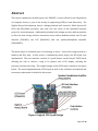
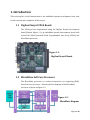
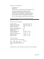
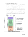
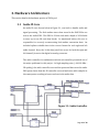
FPGA-pod EDA385 - DESIGN OF EMBEDDED SYSTEMS, ADVANCED COURSE Pierre-Adrien Lefebvre: [email protected] Kristian Samppa: [email protected] Matt Moles: [email protected] 19-10-2009 Abstract This report summarizes the final project for EDA385, a course offered by the Department of Computer Science, a part of the faculty of engineering (LTH) at Lund University. The Digilent Nexys2 development board, a design platform built around a Xilinx Spartan 3E FPGA and MicroBlaze processor, was used over the course of this embedded systems project for its development. Additionally included in the design are three add-on modules to allow for data storage and user interaction; these add-on modules include: one SD card interface (PModSD), one LCD (PModCLS), and one speaker/headphone amplifier (PModAMP1). The music player is a familiar piece of technology to most – users select songs stored in a memory and they play. In this project a rudimentary music player, the FPGA-pod, was implemented. The user interface consists of 4 push buttons on the Nexys2 FPGA board, allowing the user to choose a song to be played, and a LCD display, showing the previous/current/next song. The original design on the FPGA-pod is shown in the figure below. The actual implementation of FPGA-pod as well as the problems encountered and necessary workarounds is detailed in this report. Figure: Original FPGA-pod Design Page 2 of 18 Table of Contents Abstract………………………………………………………………………………………………………………….……...2 Table of Contents………………………………………………………………………………………..............................3 1. Introduction……………………………………………………………………………….………………………………4 1.1 Digilent Nexys2 FPGA Board……………………………………………………………………………4 1.2 MicroBlaze Soft Core Processor……………………………………………………………………….4 1.3 Embedded Development Kit (EDK)………………………………………………………………….5 1.4 FPGA-pod Global Architecture…………………………………………………………………………5 2. Software Implementation..…………………...……………………………………………………………………..7 2.1 SD Communication & Controller…...….…...…………………………………………………………7 2.2 FAT File System……………………………………………………………………………………………...8 2.3 WAVE Files & WAVE File Library…….………………………………………………………………9 2.4 Desktop Testing…………………………………………………………………………...……………….10 2.5 User Interface……………………………………………………………………………………………….11 3. Hardware Architecture…….……………………………………………………………………….………………12 3.1 Audio IP-Core……………………………………………………………………………….………………12 3.2 Digital-to-Analog Converter.………………………………………………………………………….13 4. Installation & User Manual……………………………………………….……………………………………….14 4.1 Installation…………………………………………………………………………………………………...15 4.2 User Manual….……………………………………………………………………………………………...15 5. Problems & Suggestions….………………………………………………………………………………………...15 5.1 SD Controller ………………………………………………………………………………….……………15 5.2 Little-Endian Convention………………………………………………………………………………16 5.3 Extended WAVE File Format…………………………………………………………………………16 5.4 Digital-to-Analog Converter…………………………………………………………….…………….16 6. Lessons Learned……………..….………………………………………………………………………………….…17 6.1 Time Constraints.………………………………………………………………………………………….17 6.2 Design & Implementation....…………………………………………………………………………..17 7. Conclusions………………………………………………………………………………………………………………17 8. Contributions……………..….…………………………………………………………………………………………18 Page 3 of 18 1. Introduction This section gives a brief introduction to the embedded systems development tools used for the creation and completion of this project. 1.1 Digilent Nexys2 FPGA Board The FPGA-pod was implemented using the Digilent Nexys2 development board (Shown, Figure 1.1), an embedded systems development board built around the Xilinx Spartan3E Field Programmable Gate Array (FPGA) and MicroBlaze processor. Figure 1.1: Digilent Nexys2 Board 1.2 MicroBlaze Soft Core Processor The MicroBlaze processor is a reduced instruction set computing (RISC) based soft core processor. A block style flow diagram of the MicroBlaze Processor is shown in Figure 1.2. Figure 1.2: MicroBlaze Diagram Page 4 of 18 1.3 Embedded Development Kit (EDK) The Xilinx Embedded Development Kit (EDK) allows for the development of applications and embedded systems utilizing the MicroBlaze processor. Hardware and software were writing in C and VHDL programming languages. 1.4 FPGA-pod Global Architecture Global architecture is shown in Figure 1.4 below. Figure 1.4: FPGA-pod Global Architecture Page 5 of 18 Hardware cores used in project: - MicroBlaze 7.10.d PLB bus v4.6 BRAM controller 2.10, BRAM block (32 KB program memory) xps_gpio : driving SD "pins, push-buttons and LEDs xps_uartlite : driving PMOD-CLS, speed = 9600 bds clock_generator : crystal 50 MHz => 75 MHz system clock xps_intc : interrupt controller (not used but if we need it...) audio_output_ip : User IP core designed under Xilinx ISE proc_sys_reset : handle reset when the board is powered-up Hardware & Software Occupancy - Device Utilization Summary : Hardware Occupancy: Selected Device : 3s1200efg320-4 Number of Slices: Number of Slice Flip Flops: Number of 4 input LUTs: Number used as logic: Number used as Shift registers: Number used as RAMs: Number of IOs: Number of bonded IOBs: Number of BRAMs: Number of MULT18X18SIOs: Number of GCLKs: Number of DCMs: 1576 out of 8672 18% 1984 out of 17344 11% 2500 out of 17344 14% 2138 106 256 30 30 out of 250 12% 18 out of 28 64% 3 out of 28 10% 6 out of 24 25% 2 out of 8 25% Software Occupancy : MB-size M:/EDA385/FPGA_POD/out.elf text data bss dec hex filename 25170 1368 3856 30394 76ba M:/EDA385/FPGA_POD/out.elf Done! Program memory : 32kB, “optimize size” option used for the compilation Page 6 of 18 2. Software Implementation This section details the software portion of FPGA-pod. 2.1 SD Card Communication & Controller Secure digital (SD) cards (Card Shown, Figure 2.1) have 9 pins in total - 3 pins for power and 6 pins for SD card-host communication. The SD card was operated in one wire SD mode. Data transfer between the SD card and host is made via synchronous byte oriented serial communication. In order to communicate with the SD card (Communication Shown, Figure 2.1), it must first be initialized by using a precise sequence of transmitted signals. After initialization, the host can communicate with the SD card by sending a fixed length (6 bytes) packet to the SD card with its argument and computer CRC7 through the CMD line. A response from the SD card can then be read if the command is valid and no transmission errors occurred (verified by checking the CRC7. Figure 2.1: SD Card Communication A SD card controller provides for the reading of data blocks on either a SD or SDHC (Secude Digital High Capacity) cards. The SD controller was originally implemented in hardware to acheieve the fastest data and signal processing possible, but proved very difficult to debug. Subsequently, a slower, but easier to implement SD controller was created in software. The software SD controller drives each pin of the SD card. There is no need for a regular clock Page 7 of 18 signal on the CLK pin of the SD card. To use, first the SD card is identified and initialized, data can then be read by sending block-read (512 bytes) commands to the SD host data bus. In the beginning, the SD card did not respond to commands given by the software controller. After inspection it was found that this was due to a misconfiguration of pin direction and polarity due to little-endian registers in the XPS GPIO IP-core. 2.2 FAT File System The SD card was formatted with the FAT32 file system. An independent FAT file system library (software) was then used to read files and directories on the SD card. This FAT file system and file library is platform independent; no implementation of disk I/O is made by the file system or library, it is expected that disk I/O will be implemented by the user or host. This file system and accompanying library can therefore be instantiated on any kind of memory. The FAT library and file system was successfully operated using a “black box” approach, it was very easy to use. The main functions and operating principle on the FAT library is shown below in Figure 2.2. Figure 2.2: FAT File Library **Many thanks go to Samuel from “I Deer You” for help with this section Page 8 of 18 2.3 WAVE Files & WAVE File Library WAVE (Waveform Audio File Format) files are an audio-specialized file format subset of RIFF (Resource Interchange File Format) files, generic Microsoft multimedia files. WAVE file format was the chosen format for music due to the simplicity of WAVE file format and their ease of use – also, no group member had much experience with complex audio formats or compression issues. Most simply, a wave file begins with a header section, including fields containing attributes and parameters, and is then followed by samples of sound. Of especial importance is the ChunkSize field, it contains the entire file size in bytes, minus 8 bytes for the previous ChunkID and ChunkSize fields. Standard WAVE file format is shown below in Figure 2.3. Figure 2.3: Standard WAVE File Format Page 9 of 18 New WAVE ,files, however, do not exactly follow the standard WAVE file format described above, they follow an “extended WAVE file format”. This presented a few problems for us in trying to read the size of the data segment in the WAVE file header. This problem was remedied by assuming an extra 2 bytes of data existed before the audio data section began. Additionally creating problems for us was the little-endian convention of most fields. Little-endian storage convention means that bytes are stored with their least significant bit first and later have to be ‘reconstructed’ to the correct form before manipulation of processing. Reconstructing data of 16 and 32-bit integers was accomplished in the audio controller, detailed in the hardware section of this report. An independent WAVE file library was implemented, allowing the FPGA-pod to look for WAVE files with the correct sample rate, read WAVE files, and send audio data to the audio controller, detailed in the hardware section. Population of a playlist is made possible through the use of this WAVE file library. Using functions from the library, the SD card is scanned and then an entry is made in the playlist corresponding to a WAVE file in the directory to later be used for user interfacing. 2.4 Desktop Testing The FatFS library enables files from the SD-card to be read when the SD controller is hosting the Fat file system by implementing the disk I/O. In reality, it is difficult to test portions of applications on the Nexys2 board. Therefore a mock implementation of the disk I/O data was stored in a static char vector and this application was tested on a desktop computer. In order to be able to emulate this static char vector as drive it can be formatted with the f_mkfs (mk-make fs-file system) FatFS function. In the beginning when the test program is started, the static char array is initialized to all zeros (c standard), and the FatFS library treats it as a drive that is not yet formatted. When running the system on the board there is not enough memory for the Page 10 of 18 f_mkfs function, nor all the test data that is later stored, but when running the application on the board the SD card is initialized with a file system when the application starts and data can then be stored on it. After initializing the mock disk implementation files are written to it. Because of experience, Java programming language and the JNI (Java Native Interface) was used – the FatFS functions are wrapped in Java classes, making debugging easier (at least for Java programmers). The Java classes include file implementation and an Input-/Output-Stream used to create files and directories as well as writing data into them. After all the data is written into the mock drive the C coded application to be tested can be called. Seen from the FatFS layer, there is difference between running an application to be tested on the real board. 2.5 User Interface The user interface was implemented entirely in software. Polling-based push buttons on the Nexys2 FPGA board allow the user to play/pause the currently selected song or skip to the next/previous song in the aforementioned playlist. Once a song is selected, its title is sent to LCD by means. The LCD is driven by the on-board UART (hardware), operating at 9600 bds. Printing the song title on the LCD is accomplished with the xilprintf( ) function, this is because stdout is set to be the UART. Page 11 of 18 3. Hardware Architecture This section details the hardware portion of FPGA-pod. 3.1 Audio IP-Core An audio IP-core, shown below in Figure 3.1, was built to handle audio and signal processing. The little-endian stereo data stored in the WAVE files are sent to the audio FIFO. This FIFO is 32 bits wide with a depth of 1024 fields to store up to two SD card data blocks. As mentioned before, this core is responsible for correctly reconstructing little-endian convention data. An included splitter rebuilds data in the correct format for each right and left audio channel. Next, the 16-bit data (one 8-bit vector for both the right and left channel) is sent to the digital-to-analog converter. The audio controller in combination with the sd controller presented one of the major problems for this project. At high sampling rates (~44,100 KHz – CD-quality), the audio controller can read the processed data stored in audio FIFO queue faster than the SD controller can read and store audio samples in the same queue, resulting in losses and cuts in the audio data. Figure 3.1: Audio Controller Page 12 of 18 3.2 Digital-to-Analog Converter As seen above in Figure 3.1 and below in Figure 3.2, audio samples are passed to a pair of digital-to-analog converters (DACs) after they are processed by the audio controller. These DACs produce analogue otuput signals from digital input signals via pulse-with modulation. Because no external DAC module was available, a DAC was implemented in hardware on the FPGA board. The DACs implemented here use a traditional sigma-delta structure often employed for audio applications. An application note made by Xilinx was used to design these DACs. Two 16-bit DACs using a clock frequency of 150 MHz were designed. This frequency seems to be very high but is (in theory) is needed to decrease audible noise. Audio output through a pair of speakers or headphones connected to the amplifier is audible and recognizable, but very noisy. We believe this is due to the lack of a traditional external DAC and subsequent proper signal filtering. Audio signals are not filtered properly and a lot of noise exists in the output. The DAC was this projects largest problem and at the time of this report is still unsolved. Here is a list of what we’ve tried to make this block work: Decrease the block frequency Reduce the precision of DACs down to 8 bits Changing the sampling frequency of the wave files. Page 13 of 18 Figure 3.2: DigitalTo-Analog Converter 4. Installation & User Manual Figure 4: FPGA-pod Setup Page 14 of 18 4.1 Installation No installation is necessary. Simply load a SD or SDHC card with your favorite, properly formatted audio into the SD card reader and power on the FPGA-pod. 4.2 User Manual 1. Ensure all components are connected as shown in Figure 4 2. Insert SD or SDHC card preloaded with WAVE stereo audio sampled (16bits) at 6,000 KHz into the SD card reader 3. Insert headphone or speaker jack into amplifier receiving jack 4. Power and turn on Nexys2 FPGA board, 1st audio file is played automatically 5. Use the left most push-button to play or pause the currently selected song 6. Use the middle 2 buttons to skip to the next or previous song 7. Use the right most push-button to reset the FPGA-pod 5. Problems & Suggestions 5.1 SD Controller The SD controller was originally planned to be implemented in hardware. Work was accomplished on a hardware SD card controller, but it proved very difficult to debug. Because of this, a SD controller was implemented software. While this software controller was much easier to test and debug, the controller was also slow – the software is responsible for driving each SD pin directly. When using high sampling rates, ~44,100 KHz (CD quality), reading audio in the audio sample FIFO queue happened faster than the SD controller could write this data to the queue. This resulted in cuts of data and audio flow as well as loss of audio data. In efforts to remedy this issue, the FIFO audio queue size increased from 512 to 1024 32-bit samples and the MicroBlaze system clock was also been increased from 50 MHz to 75 MHz Page 15 of 18 (this frequency cannot be increased further due to timing constraints). Using a maximum sampling frequency of 8,000 KHz prevents the audio FIFO queue from emptying. This issue would be easily solved given more time to debug and implement a SD controller designed in hardware 5.2 Little-Endian Convention Many problems were encountered over the development process due to Xilinx’s little-endian standard. Little-endian standards were also found in the WAVE file requiring the implementation of an audio splitter to reconstruct reverse-byte stored 16 and 32 bit data fields. 5.3 Extended WAVE File Format The WAVE file format detailed in this report is the standard WAVE file format. New WAVE files, however, follow a slightly more obscure and quite different version of this format known as “extended WAVE file format”. Due to this standard, difficulties were experienced when trying to read the size of the data segment in the WAVE file following the header information. 5.4 Digital-to-Analog Converter The digital-to-analog converter presented out biggest and at the time of writing still unsolved problem. The lack of a traditional external digital-toanalog converter means lack of proper signal filtering. Pulse-widthmodulation dignals produced by the on-board hardware implemented DACs are connected directly to the inputs of the PmodAmp module. Because these signals are not properly filtered by the on-board DACs before they are sent to amplifier, a lot of noise exists in the output. We believe this issue would be easily solved through the implementation of an external digital-to-analogue converter module. Page 16 of 18 6. Lessons Learned 6.1 Time Constraints Estimating the amount of time required to complete embedded systems projects, or any portion of a single project, is a difficult thing to do and time required is easily underestimated 6.2 Design & Implementation The Pros and cons of a design must be considered when choosing to implement that design in primarily either hardware or software. For certain applications hardware implementation is a much better choice. For other projects with demanding deadlines software implementation is often easier to implement and debug. In the case of the SD controller, a design in hardware would have functioned better, but quickly implementing a design in software functionality to be proven within the given time constraints. 7. Conclusions Program memory was increased to a maximum of 32 KB. This memory cannot be further expanded due to a lack of BRAMs. The finished FPGA-pod project is quite large, at least for the Nexys2 board, occupying about 29 of the available 36 KB or memory – this project will not successfully compile unless the size optimization parameter (-os) is specified. The most challenging portion of this project has been the implementation of the SD controller. Due to quickly approaching deadlines the hardware SD controller was not finished Page 17 of 18 Designing and successfully creating hardware in the real world is more difficult, but also much more rewarding than simply designing hardware on paper. Suggested future work and improvements for this project include the successful implementation of a hardware-based SD controller, the addition of an external digital-to-analog converter complete with proper signal filtering capabilities, decompression capabilities providing support for mp3 or additional file formats, and added user/menu actions 8. Contributions **The drafting of documents (initial proposal & presentation, final report & presentation, etc.) was assisted by all group members. Pierre-Adrien Lefebvre : SD Controller, Audio Controller, FAT File System Kristian Samppa: SD Controller, Audio Controller, LCD Interface Matt Moles: Push Buttons, User Menus, LCD Interface Page 18 of 18