1
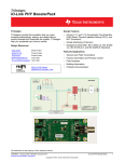
TI Designs
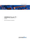
Hall-Effect Proximity Sensor With IO-Link™ Design Guide
TI Designs
Design Features
TI Designs provide the foundation that you need
including methodology, testing and design files to
quickly evaluate and customize the system. TI Designs
help you accelerate your time to market.
•
•
•
Design Resources
Latch Magnetic Field Hall-Effect Proximity Sensor
Multi-Variable IO-Link Sensor Transmitter
IO-Link v1.1 Connectivity Out of the Box
(TMG Stack, PHY, and M12 Connector)
Featured Applications
TIDA-00340
SN65HVD101
MSP430FR5738
Tool Folder Containing Design Files
DRV5013
Product Folder
•
•
•
•
Product Folder
Product Folder
Factory Automation and Process Control
Building Automation
Sensors and Field Transmitters
Portable Instrumentation
ASK Our E2E Experts
WEBENCH® Calculator Tools
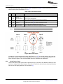
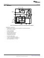
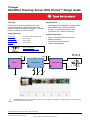
VCC
VCC
xVCC
xVCC
DRV5013
MSP430FR5738
OUT
t
t
M12-4
VCC
VCC (LDO out)
2: NC
L+
3: L-
TX
RX
EN
SN65HVD101 C/Q
t
L-
1: L+
4: C/Q
An IMPORTANT NOTICE at the end of this TI reference design addresses authorized use, intellectual property matters and other
important disclaimers and information.
All trademarks are the property of their respective owners.
TIDU671 – March 2015
Submit Documentation Feedback
Hall-Effect Proximity Sensor With IO-Link™ Design Guide
Copyright © 2015, Texas Instruments Incorporated
1
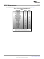
Key System Specifications
1
www.ti.com
Key System Specifications
Table 1. Key System Specifications
PARAMETER
VCC
Iq_SIO
Iq_IOLink
Vdrop
PNP_NPN
SPECIFICATION
VALUE
DETAILS
24 V
Section 3.1.1
Nominal operating current (SIO mode)
5 mA (LEDs OFF)
Section 5.1
Nominal operating current (IO-Link mode
COM3)
7.5 mA (LED OFF)
Section 5.4
< 2.5 V
Section 3.1.1
PNP (NPN settings possible)
Section 3.2
Nominal operating
Voltage drop
Switching output in SIO mode
NO_NC
Switching function
NO (NC settings also possible)
Section 3.2
TA
Temperature range
–40°C to 85°C
Section 3.1.2
Form factor
M12
Section 6.3
Connector
M12
Section 6.1
Reverse protection
Yes
Section 5.3
2
System Description
2.1
System Overview
The system provides a hall-sensor IC, which then can drive the IO-Link through the MSP430. Two LEDs
are on the board: one showing the IO-Link activity and the other one being an image of the Hall sensor
output. The IO-Link offers the capability for the sensor to provide logging information as well as
temperature sensing using the MSP430 on-chip temperature sensor for multi-variable sensing for the
IO-Link master.
2.2
IO-Link
CAUTION
To facilitate a ground-up IO-Link device project, this section provides a quick
overview of the IO-Link interface. This section should, under no condition, be
considered a reference. Only the reference documents should be used after the
initial phase of the project.
IO-Link (1) is a simple and cheap point-to-point protocol (standardized as IEC 61131-9) for the industrial
automation and control applications.
Though the IO-Link clearly states that a master can have several ports, each of which can have a unique
device connected to it, the rest of this document refers to a connection between the master and the device
to avoid a heavy "master-port" naming of a potentially misleading "port" denomination.
(1)
2
IO-Link is a trade name of the IO-Link Community. This information is given for the convenience of users of this international standard
and does not constitute an endorsement by IEC of the trade name holder or any of its products. Compliance to this standard does not
require use of the registered logos for IO-Link. Use of the registered logos for IO-Link requires permission of the IO-Link Community. [1]
Hall-Effect Proximity Sensor With IO-Link™ Design Guide
Copyright © 2015, Texas Instruments Incorporated
TIDU671 – March 2015
Submit Documentation Feedback
System Description
www.ti.com
2.2.1
IO-Link Physical Connectors
The IO-Link connectors pin assignment is based on IEC60947-5-2 [4] with extensions specified in IO-Link
Interface and System Specification v1.1.2 [1]. Figure 1 is a capture of the M12 connector selected for this
project from IEC60947-5-2 [4].
8 min.
6,5 ± 0,2
3 max.
90°
∅1,00 ± 0,03
∅0,1 A
TYP. 4 PLC
4
A
1,65 +0,10
0
1
0
∅10,5 –0,3
3
∅7,60 +0,15
M12,0 × 1
2
0
R4,40 +0,10
0
∅4,57
2,55 +0,10
0
5,5 ± 0,2
7,2 0
–0,2
NOTE 2
Sealing face
NOTE 1 Pin identification numbering is not necessary.
NOTE 2 For a provisional period, the use of 1/2”-20UNF-2A is permissible as an alternative to M12 on a.c.
proximity switches.
NOTE 3
The protective earth pin shall be omitted for class II proximity switches.
Figure 1. M12 ∅ 4-Pin Integral Connector (Defined by IEC 60947.5.2)
TIDU671 – March 2015
Submit Documentation Feedback
Hall-Effect Proximity Sensor With IO-Link™ Design Guide
Copyright © 2015, Texas Instruments Incorporated
3
System Description
www.ti.com
The electrical connections are described in Table 2 and shown in Figure 2, both extracted from IO-Link
Interface and System Specification v1.1.2 [1].
Table 2. M12 4-Pin Assisgnments
PIN
SIGNAL
DESTINATION
REMARK
1
L+
Power supply (+)
See Table 7 from source [1]
2
I/Q
P24
NC/DI/DO (port
class A)
P24 (port class B)
Option 1: NC (not connected)
Option 2: DI
Option 3: DI, then configured DO
Option 4: Extra power supply for power devices (port Class B)
3
L–
Power supply (–)
See Table 7 from source [1]
4
C/Q
SIO/SDCI
Standard I/O mode (DI/DO) or SDCI
See Table 6 from source [1] for electrical characteristics of DO.
5
NC
N24
NC (port class A)
N24 (port class B)
Option 1: Shall not be connected on the master side
Option 2: Reference to the extra power supply (port Class B)
NOTE: M12 is always a 5-pin version on the master side (female).
Figure 2. M12 4-Pin Layout
According to IO-Link Interface and System Specification v1.1.2 [1], the current project is only using the
port Class A definition. Cables are also specified by IO-Link Interface and System Specification v1.1.2,
with a maximum length of 20 m and associated maximum resistance and capacitance.
2.2.2
IO-Link Device Power
The IO-Link device (Class A) can draw its power from the L+ line and is only allowed to draw up to 200
mA from a voltage, which varies between 18 and 30 V. The IO-Link device must be functional less than
300 ms after the supply passes the 18-V threshold. [1]
4
Hall-Effect Proximity Sensor With IO-Link™ Design Guide
Copyright © 2015, Texas Instruments Incorporated
TIDU671 – March 2015
Submit Documentation Feedback
System Description
www.ti.com
2.2.3
IO-Link Communication Layer
The IO-Link communication can be seen as having two modes. The first mode is a back-up, quasi-static
mode that ensures backward compatibility with standard I/O (SIO) mode specified in IEC61131-2 [5]. The
second mode is the newly defined dynamic mode for bi-directional communication (SDCI) defined by [1].
A good overview is provided by Figure 3 (combined from [1] and [5]).
Pin
L+
DI/DQ
SIO
1
5
2
C/Q
4
COMx
3
4.8 / 38.4 / 230.4 kbps
Signal
Definition
Standard
1
L+
24 V
IEC 61131-2
2
I/Q
Not connected, DI, or
DO
IEC 61131-2
3
L-
0V
IEC 61131-2
4
Q
"Switching signal" DI
(SIO)
IEC 61131-2
C
"Coded switching"
(COM1, COM2, COM3)
IEC 61131-9
L-
Figure 3. SIO versus SDCI (or IEC61131-9 versus IEC61131-2)
The switch between SIO mode and SDCI is master initiated.
The master issues a wake-up command to the device, which consists in shorting the 80-µs CQ line with at
least 500 mA (IQPKHM) [1]. The device must be ready for communication in less than 500 µs (TREN).
After the wake-up request (WURQ), the master waits for the device to be enabled for TREN [1]. The
master then tries to identify the highest transmission rate supported by the device by sending a test
message (M-sequence type 0). See Section 2.2.3.2 for details.
Following the wake-up attempt, should communication fail, the device switches back to SIO mode within a
time window of 60 to 300 ms (TDSIO) [1].
If communication is successful, it occurs on a frame basis.
2.2.3.1
2.2.3.1.1
Physical Layer
Handshake
The master issues a wake-up command to the device, which consists in shorting the CQ line for 80 µs
with at least 500 mA (IQPKHM) [1]. The device must be ready for communication in less than 500 µs
(TREN).
The short from the master will be made in such a way that the master shorts the CQ line to the opposite
value driven by the device to ensure the device senses the current surge the master is driving on the CQ
line (see Figure 4).
SIO Mode
Device output
V
Wake-up request
a)
Ready to communicate
b)
Q = low
undefined
High impedance, low level
Q = high
undefined
High impedance, low level
t
TWU
TREN
Figure 4. Wake-Up Request
TIDU671 – March 2015
Submit Documentation Feedback
Hall-Effect Proximity Sensor With IO-Link™ Design Guide
Copyright © 2015, Texas Instruments Incorporated
5
System Description
2.2.3.1.2
www.ti.com
Modulation
Communication is done with a universal asynchronous receiver or transmitter (UART) frame consisting of
11 bits (1 start bit + 8 bit data + 1 bit parity + 1 STOP bit).
Bits are transmitted over the CQ line with a simple non-return-to-zero, or NRZ (that is, a logical '0' is 24 V
between CQ and L–, and a logical '1' is 0 V between CQ and L–).
Bit durations are defined by the transmission rate (the highest transmission rate at which the device can
detect the test message sent by the master). The eye diagrams are illustrated by Figure 5 and Figure 6.
tH
tL
tND
tND
VIH D,M MAX
V+ D,M
VRQHD,M MAX
Detection 'H'
VTHH MAX
2)
VTHH MIN
VTHL MAX
VTHL MIN
1)
Detection 'L'
VRQL D,M MAX
V0 D,M
VIL D,M MIN
tDF
tDR
TBIT
TBIT
In the figure, 1) = no detection 'L'; and 2) = no detection 'H'
Figure 5. Eye Diagram for the 'H' and 'L' Detection
‘0’: start bit
Start
Bit n=1
TBIT
CQ
Bit n=2
ST = ‘1’
P
Bit n=3
Bit n=9
Stop
Bit n=11
Bit n=10
TBIT
VTHH
VTHL
L–
(2-r)TBIT
(1-s)TBIT
(2-s)TBIT
(3-r)TBIT
(3-s)TBIT
(10-r)TBIT
(11-r)T BIT
(10-s)TBIT
(11-s)TBIT
Figure 6. Eye Diagram for the Correct Detection of a UART Frame
6
Hall-Effect Proximity Sensor With IO-Link™ Design Guide
Copyright © 2015, Texas Instruments Incorporated
TIDU671 – March 2015
Submit Documentation Feedback
System Description
www.ti.com
2.2.3.2
2.2.3.2.1
Data Link Layer
Transmission Frame
Communication between a master and its associated device takes place in a fixed schedule, called the
message sequence (M-sequence) time (tM-sequence) defined in IO-Link Interface and System Specification
v1.1.2 [1] of which Figure 7 is an extract.
UART
frame
Port
(Master)
UART
frame
UART
frame
t1
t1
UART
frame
Device
UART
frame
t2
UART
frame
t2
tA
tM-sequence
Figure 7. M-Sequence Timing
2.2.3.2.2
Transmission Rate Negotiation
After the WURQ, the master sends a test message with M-sequence TYPE_0 and should the device be
capable of deciphering, the device should answer within tA to the master (see Figure 8 and Figure 9).
TREN
1
WURQ
3
2
Master
start-up
Master
TDMT
TDMT
COM3
TDMT
COM1
COM2
4
SIO
Device
start-up
Device
Figure 8. Example of Successful Transmission Rate Negotiation
WURQ
WURQ
Master
COM3
COM1
COM2
SIO
No response
Device
TDWU
Figure 9. Example of Failed Transmission Rate Negotiation
TIDU671 – March 2015
Submit Documentation Feedback
Hall-Effect Proximity Sensor With IO-Link™ Design Guide
Copyright © 2015, Texas Instruments Incorporated
7
System Description
2.2.3.2.3
www.ti.com
Data Link Layer Services
Once established, the master and devices have access to services summarized in Table 3.
Table 3. Service Assignments Within Master and
Device
SERVICE NAME
MASTER
DEVICE
DL_ReadParam
R
I
DL_WriteParam
R
I
DL_ISDUTransport
R
I
DL_ISDUAbort
R
I
DL_PDOutputUpdate
R
DL_PDOutputTransport
I
DL_PDInputUpdate
R
DL_PDInputTransport
I
DL_PDCycle
I
DL_SetMode
R
I
DL_Mode
I
I
DL_Event
I
R
DL_EventConf
R
DL_EventTrigger
R
DL_Control
I/R
R/I
DL_Read
R
I
DL_Write
R
I
Key
8
I
Initiator of a service (towards the layer above)
R
Receiver (responder) of a service (from the layer above)
Hall-Effect Proximity Sensor With IO-Link™ Design Guide
Copyright © 2015, Texas Instruments Incorporated
TIDU671 – March 2015
Submit Documentation Feedback
System Description
www.ti.com
2.2.3.3
Application Layer
Once established, the master can then access the structure and services of the device application layer as
illustrated by Figure 10.
Technology specific application (technology parameter, diagnosis, process data)
System
management
DL_Mode
PL_SetMode.req
MHInfo
PL_WakeUp.ind
AL_PDCycle
AL_NewOutput
DL_PDCycle
DL_PDOutputTransport
Process Data
handler
PD.ind
PD.rsp
DL-B
EventFlag
PDInStatus
Device
DL-mode
handler
OD.rsp
DL_Write
OD.ind
DL_Read
SIO:
DI / DO
Process Data
objects
DL_PDInputUpdate
DL_EventTrigger
DL_Event
DL_Control
-
DL_ISDU
Abort
DL_ISDU
Transport
DL_WriteParam
DL_Read
Param
On-request Data
handler
Line
Handler
AL_GetOutput
AL_SetInput
AL_Event
AL_Control
AL_Write
Process Data Exchange (PDE)
On-request Data
AL
objects Application Layer
SM_DeviceMode
SM_SetDeviceMode
SM_SetDeviceCom
SM_GetDeviceCom
SM_SetDevciceIdent
SM_GetDeviceIdent
Event Dispatcher (ED)
AL_Abort
Data Storage (DS)
AL_Read
Parameter Manager (PM)
DL-A
Message
handler
PL_Transfer.ind
PL_Transfer.req
SIO:
DI / DO
Mode switch
Wake-up
Coded switching
Switching signal
Physical layer
Figure 10. Structure and Services of the Device Application Layer
TIDU671 – March 2015
Submit Documentation Feedback
Hall-Effect Proximity Sensor With IO-Link™ Design Guide
Copyright © 2015, Texas Instruments Incorporated
9
System Description
2.3
www.ti.com
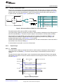
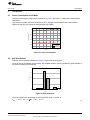
Hall
Hall-effect sensing technology detects the presence of a magnetic field. This technology is mainly used to
sense position, speed, and acceleration.
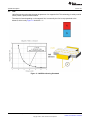
The output is linear depending on the magnetic flux, but normally the flux is not proportional to the
distance, which is why Figure 11 looks like 1 / x.
Figure 11. Hall-Effect Sensing Illustrated
10
Hall-Effect Proximity Sensor With IO-Link™ Design Guide
Copyright © 2015, Texas Instruments Incorporated
TIDU671 – March 2015
Submit Documentation Feedback
System Description
www.ti.com
2.3.1
Common Terminology and Conventions Used
•
Standard convention to indicate polarity:
– North pole: denoted by a negative magnetic field
– South pole: denoted by a positive magnetic field
NOTE: The magnets used do not have to be rare earth magnets.
•
•
•
•
•
•
•
BOP: Magnetic field ('B' field) operate point, as B field increases, BOP is the threshold when the output
goes Low-Z
BRP: Magnetic field ('B' field) release point, as B field decreases, BRP is the threshold when the output
goes High-Z. BRP is of opposite leading sign (main difference between latch and switch)
BHYS: Magnetic field hysteresis = BOP – BRP
– Prevents magnetic-field noise from accidentally tripping the output between BOP and BRP
BO: Magnetic field offset = (BOP – BRP) / 2
– The center point of thresholds
– Another parameter / equation used to define hysteresis of the sensor
Linear sensitivity: The voltage gain per magnetic field strength, in mV / mT
Zero magnetic field outputs VQ, the quiescent voltage output
Magnetic (B) field sensitivity:
– Parameters used for digital Hall-effect sensors: BOP and BRP
– Parameter used for analog Hall-effect sensors: In mV / mT; the magnetic field strength is affected
by
• Shape, magnetization, and composition of the magnetic object
• Distance from object to Hall-effect sensor
NOTE: 1 mT = 10 gauss
Tesla is the SI unit for the magnetic B field.
•
•
Higher sensitivity corresponds to a lower number:
– For example, a 3-mT BOP sensor is more sensitive than a 150-mT BOP sensor
– A 3-mT Hall-effect sensor will hit its trip point much sooner than the 150-mT Hall-effect sensor as a
magnet is brought closer to the sensor
Required sensitivity depends on the design
– Highly sensitive Hall-effect sensors can sometimes help to cut down system cost, allowing designs
to use cheaper (lower strength) magnets
– To prevent magnetic-field noise from potentially tripping the sensor sooner than required, some
applications require less sensitive Hall-effect sensors in its design
TIDU671 – March 2015
Submit Documentation Feedback
Hall-Effect Proximity Sensor With IO-Link™ Design Guide
Copyright © 2015, Texas Instruments Incorporated
11
System Description
2.3.2
www.ti.com
Hall-Effect Sensor: Head-On versus Slide-By
Head-on sensing is the most usual way to test a Hall-effect sensor transmitter. Head-on sensing involves
taking a permanent magnet and bringing a pole up to the sensing part to activate that part. Usually in a
head-on operation, the sensitive axis of the Hall-effect sensor is parallel to the axis of the magnet.
If the field strength was plotted over the distance (air gap), in what is often referred to as a flux map, one
would have a rapidly decreasing curve as the distance increases.
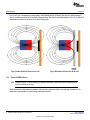
Slide-by sensing is another way to use a Hall-effect sensor transmitter. In this configuration, the magnet
north-south axis and the sensitive axis of the Hall-effect sensors are parallel, but the magnet is moving in
a plane orthogonal to that axis. This system can be particularly useful to detect when a system is passing
it is out of range position. When the Hall-effect sensor detects the maximum field, the sensor triggers a
system notification that a moving part left the designated area.
While both head-on and slide-by sensing provide relative information, some systems will need absolute
information in which case null-point sensing is used. For this information, think of the Hall-effect sensor as
being equally distanced from the south and north pole of the magnet. When equally distanced, the sensor
will see a "zero field" and as soon as the magnet moves (one pole will get closer to the Hall-effect sensor
and the other pole will move away), creating a resulting field either positive or negative.
12
Hall-Effect Proximity Sensor With IO-Link™ Design Guide
Copyright © 2015, Texas Instruments Incorporated
TIDU671 – March 2015
Submit Documentation Feedback
System Description
www.ti.com
2.3.3
Hall-Effect Sensor Sensitive Usage
While Hall-effect sensing now has a broad range of usage in the industry, the goal of this section is to
illustrate a few usual applications for engineers needing to design such systems for a first time.
Figure 12 is an example of a float sensing through a ring magnet. When the float part where the hallsensor is mounted is in the middle of the ring magnet, the flux will be nill, allowing the sensor to detect a
level very accurately.
Figure 12. Float Sensing Through a Ring Magnet
Figure 13 is an example of linear sensing. When the Hall sensor that moves along the axis d is inside the
magnets, the sensor will see a null field. Figure 14 is an example of angle sensing.
Figure 13. Example of Linear Sensing
TIDU671 – March 2015
Submit Documentation Feedback
Figure 14. Example of Angle Sensing
Hall-Effect Proximity Sensor With IO-Link™ Design Guide
Copyright © 2015, Texas Instruments Incorporated
13
System Description
www.ti.com
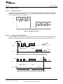
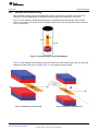
Figure 15 and Figure 16 are examples of proximity sensing of a metal obstacle based on Hall sensing. When there is no metal obstacle (top of
Figure 15), the Hall sensor will see the field and output a voltage accordingly. When there is a metal obstacle (bottom of Figure 15), the field will be
concentrated in the metal and the Hall sensor will not see the field any longer.
Figure 15. No Metal Obstacle (Hall Sensor Does See Field)
2.3.4
Figure 16. Metal Obstacle (Hall Sensor Does Not See Field)
Physics of Hall-Effect Sensors
NOTE: Temperature coefficients: TI Hall-effect sensors all have temperature compensation, so they are far less sensitive to temperature effects
than physics would make the raw sensor.
Hall-effect sensors have a slight temperature dependency that could create a measurement artifact over a broad range of temperatures. The
consequence is often mentioned in a percentile change in sensitivity per kelvin (K).
space
space
space
space
14
Hall-Effect Proximity Sensor With IO-Link™ Design Guide
TIDU671 – March 2015
Submit Documentation Feedback
Copyright © 2015, Texas Instruments Incorporated
Design Overview
www.ti.com
3
Design Overview
3.1
Hardware
VCC
VCC
xVCC
xVCC
DRV5013
t
MSP430FR5738
OUT
t
M12-4
VCC
VCC (LDO out)
2: NC
L+
3: L-
TX
RX
EN
SN65HVD101 C/Q
t
L-
1: L+
4: C/Q
Figure 17. TIDA-00340 Block Diagram
TIDU671 – March 2015
Submit Documentation Feedback
Hall-Effect Proximity Sensor With IO-Link™ Design Guide
Copyright © 2015, Texas Instruments Incorporated
15
Design Overview
3.1.1
www.ti.com
SN65HVD101
VCC
OUT
VCC VCC
IN SET
L+
SUPPLY VOLTAGE
CONTROL
PWR_OK
RX
CQ
TX
Voltage
Timers
EN
WAKE
CUR_OK
Control
Logic
Voltage
Detectors
L-
Over Current Over Current
Timers
Detectors
TEMPERATURE
SENSE
TEMP_OK
ILIM_ADJ
GND
L-
Figure 18. SN65HVD101 (SIO PHY for Device Nodes) Block Diagram
SN65HVD101 key features:
• Configurable CQ output: Push-pull, high-side, or low-side for SIO mode
• Remote wake-up indicator
• Current limit indicator
• Power-good indicator
• Over-temperature protection
• Reverse polarity protection
• Configurable current limits
• 9- to 36-V supply range
• Tolerant to 50-V peak line voltage
• 3.3-V/5-V configurable integrated LDO
• 20-pin QFN package, 4 × 3.5 mm
16
Hall-Effect Proximity Sensor With IO-Link™ Design Guide
Copyright © 2015, Texas Instruments Incorporated
TIDU671 – March 2015
Submit Documentation Feedback
Design Overview
www.ti.com
3.1.2
MSP430FR5738
PJ.4/XIN
DVCC DVSS VCORE
PJ.5/XOUT
AVCC AVSS
P1.x
16 KB
Clock
System
(FR5738)
ACLK
8 KB
(FR5734)
1 KB
4 KB
SMCLK
(FR5730)
CPUXV2
and
Working
Registers
SYS
Watchdog
REF
SVS
FRAM
MCLK
Boot
ROM
Power
Management
PA
P2.x
I/O Ports
P1/P2
1×8 I/Os
1×3 I/Os
Interrupt
& Wakeup
PA
1×11 I/Os
RAM
Memory
Protection
Unit
MAB
DMA
MDB
3 Channel
EEM
(S: 3+1)
RST/NMI/SBWTDIO
TEST/SBWTCK
PJ.0/TDO
PJ.1/TDI/TCLK
PJ.2/TMS
PJ.3/TCK
JTAG/
SBW
Interface
TA0
TA1
TB0
(2) Timer_A
3 CC
Registers
(1) Timer_B
3 CC
Registers
eUSCI_A0:
UART,
IrDA, SPI
RTC_B
MPY32
CRC
eUSCI_B0:
SPI, I2C
ADC10_B
10 Bit
200KSPS
Comp_D
10 channels
8 channels
(6 ext/2 int)
Figure 19. MSP430FR5738 Block Diagram
MSP430FR5738 key features:
• Embedded MCU 16-bit RISC architecture up to 24-MHz clock
• Wide supply voltage range (2 to 3.6 V)
• Optimized ultra low-power modes [81.4 μA / MHz in active and 320 nA in shutdown (LPM4.5)]
• Ultra low-power ferroelectric RAM
• 16-KB Nonvolatile Memory
• Ultra low-power Writes
• Fast write at 125 ns per word (16 KB in 1 ms)
• Built in error coding and correction (ECC) and MPU
• Universal memory = Program + data + storage
• 1015-write cycle endurance
• Intelligent digital peripherals
• 32-bit hardware multiplier (MPY)
• Channel internal DMA
• RTC with calendar and alarm functions
• 16-bit cyclic redundancy checker (CRC)
• High-performance analog
• Enhanced serial communication
TIDU671 – March 2015
Submit Documentation Feedback
Hall-Effect Proximity Sensor With IO-Link™ Design Guide
Copyright © 2015, Texas Instruments Incorporated
17
Design Overview
3.1.3
www.ti.com
DRV5013
2.5 to 38 V
C1
VCC
Regulated Supply
Bias
R1
Temperature
Compensation
OUT
C2
OCP
Offset Cancel
Hall Element
(Optional)
+
Gate
Drive
±
Reference
GND
Figure 20. DRV5013 Block Diagram
DRV5013 key features:
• Digital bipolar-latch hall sensor
• Superior temperature stability
– BOP ±10% over temperature
– High sensitivity options (BOP and BRP )
• ±2.3 mT
• ±4.6 mT
• ±9.2 mT
– Supports a wide voltage range (2.5 to 38
V)
– Operation from unregulated supply
– Wide operating temperature range
(–40°C to 125°C)
– Open drain output
18
–
–
–
–
• Up to 30-mA current sink
Fast power-on (35 µs)
Small package and footprint
• Surface mount 3-terminal SOT-23
(DBZ)
• 2.92 × 2.37 mm
Through-hole 3-terminal SIP (LPG)
• 4 × 3.15 mm
Protection features
• Reverse supply protection (up to –22
V)
• Supports up to 40-V load dump
• Output short circuit protection
• Output current limitation
Hall-Effect Proximity Sensor With IO-Link™ Design Guide
Copyright © 2015, Texas Instruments Incorporated
TIDU671 – March 2015
Submit Documentation Feedback
Design Overview
www.ti.com
3.2
Software
For software design and documentation, please contact TMG.
3.3
3.3.1
Design for Test
Software Update
For MSP430 firmware updates, Code Composer Studio™ (CCS) is recommended. CCS is an integrated
development environment (IDE) for TI embedded processor families. CCS comprises a suite of tools used
to develop and debug embedded applications. This suite includes compilers for each of TI's device
families, source code editor, project build environment, debugger, profiler, simulators, real-time operating
system, and many other features. The intuitive IDE provides a single user interface taking the user
through each step of the application development flow. For programming and debugging, the
MSP430FR5738 implements an embedded emulation module (EEM). This EEM is accessed and
controlled through either 4-wire JTAG mode or Spy-Bi-Wire mode. This reference design only supports the
Spy-Bi-Wire mode. For more details on how the features of the EEM can be used together with CCS, see
Advanced Debugging Using the Enhanced Emulation Module [6].
The 2-wire interface is made up of the Spy-Bi-Wire test clock (SBWTCK) and Spy-Bi-Wire test data I/O
(SBWTDIO) pins. The SBWTCK signal is the clock signal and a dedicated pin. In normal operation, this
pin is internally pulled to ground. The SBWTDIO signal represents the data and is a bidirectional
connection. To reduce the overhead of the 2-wire interface, the SBWTDIO line is shared with the
RST/NMI pin of the device. For programming and debugging purposes, the SBWTCK, SBWTDIO, VCC,
and GND from the debugger need to be connected on J1.
R4
RST/NMI/SBWTDIO
TEST/SBWTCK
QFN PAD
AVSS
DVSS
47k
12
11
25
23
19
DNPC11
2200pF
GND
VCC
VCC
J1
4
3
2
1
GND
Figure 21. JTAG Connection (Pin 1 is Marked on PCB)
With the proper connections, an MSP430 debugger interface can program and debug code on the
reference design.
TIDU671 – March 2015
Submit Documentation Feedback
Hall-Effect Proximity Sensor With IO-Link™ Design Guide
Copyright © 2015, Texas Instruments Incorporated
19
Design Overview
3.3.2
www.ti.com
Power During Debugging
CAUTION
Take special care while debugging to avoid damages due to different power
domain in conflicts (IO-Link power and debugger tools power). Read this
section carefully.
The SN65HVD101 integrates a linear voltage regulator, which supplies 3.3 V to the IO-Link demo board if
a voltage in the range of 9 to 30 V is supplied to L+. Normally, the MSP430FR5738 is powered from this
3.3 V.
If this local 3.3-V supply from the SN65HVD101 is used during debug, make sure the VCC_Target pin
from the debugger interface is connected to VCC. If there is no local power and power from the debugger
interface is used, make sure the VCC_Tool pin from the debugger interface is connected to VCC and
disconnect the VCC_Target pin (see Figure 22).
VCC
MSP430
VCC
VCC/AVCC/DVCC
47 kW
JTAG
VCC TOOL
VCC TARGET
2
1
4
3
6
5
8
7
10
9
12
11
14
13
TDO/TDI
RST/NMI/SBWTDIO
TCK
GND
TEST/SBWTCK
2.2 nF
VSS/AVSS/DVSS
Figure 22. Signal Connections for 2-Wire JTAG Communication (Spy-Bi-Wire)
View From Separate "Debugger Interface" Board
20
Hall-Effect Proximity Sensor With IO-Link™ Design Guide
Copyright © 2015, Texas Instruments Incorporated
TIDU671 – March 2015
Submit Documentation Feedback
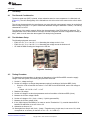
Test Setup
www.ti.com
4
Test Setup
4.1
Test General Consideration
The device under test (DUT) is placed, unless otherwise stated, at room temperature in a Helmholtz coil
(Figure 23). The coil's homogeneity of the field within a 4×4×4-mm cube in the center on the coils is within
0.6%.
The coil was characterized by the manufacturer over temp with their own magnetic sensor (air cooled) and
shows change over temp < 1% (due to mechanical dimension change of Helmholtz + sensor). The coil key
characteristic is 6 mT/A.
The influence of the earth's magnetic field on the characterization of the TIDA-00340 is neglected. This
characterization can be done because in Europe, the earth's magnetic field has a magnetic flux density of
48 µT, which is much lower than the magnetic flux density being measured.
4.2
Test Hardware Setup
The following equipment were used:
• E3631 0 to 6 V, 5 A / 0 to ±25 V, 1 A: Generating the voltage on the L+ line
• E3631 0 to 6 V, 5 A / 0 to ±25 V, 1 A: Generating the voltage across the Helmotz coil
• HP 34401A DMM: Reading the voltage on the CQ line
Figure 23. Test Setup
4.3
Testing Procedure
To characterize the dependency (or absence of dependancy) of the BOP and BRP versus the supply
voltage of the total system, the following test procedure was used:
1. Set the L+ voltage and log it.
2. Set the coil voltage to a voltage that guarantees under all conditions a field below BRP (Vmin):
• Given the 10-Ω coil and the min value of –5-mT BRP for the DRV5013AD, set the coil voltage to
–10 V:
– Indeed: –10 V/10 Ω × 6 mT = –6 mT
3. Read the CQ voltage.
4. Set the coil voltage to a value that guarantees under all condition a field above BRP (Vmax).
5. Measure the CQ line voltage CQmax.
6. Set the coil voltage to V2 = (Vmin + Vmax) / 2 (which generates B2).
7. Measure the CQ line voltage (CQ2).
8. If the | CQ2-Cqmax|>Threshold (in our case we set the Threshold to 5 V), consider that the BOP is
between B2 and Bmax so we set Vmin to V2.
9. Otherwise set Vmax to V2.
10. Start again from Step 6 until |Vmin – Vmax| < TargetAccuracy (In this case, it was set to 0.01, which
corresponds to an accuracy on the BxP of 0.01 / 10 × 6 = 0.006 mT).
TIDU671 – March 2015
Submit Documentation Feedback
Hall-Effect Proximity Sensor With IO-Link™ Design Guide
Copyright © 2015, Texas Instruments Incorporated
21
Test Setup
4.4
4.4.1
www.ti.com
System Setup
Hardware and Software
For the initial setup, the following hardware and software is required:
• TIDA-00340
– IO-Link stack including application firmware (contact TMG)
• USB IO-Link Master (here: TMG – USB IO-Link Master V2 SE)
– GUI for USB IO-Link Master (here: TMG IO-LINK Device Tool V4.0)
– IODD (contact TMG)
• M12 cable (female – male)
Figure 24. Setup
4.4.2
Software Installation
Please refer to the user manual of the chosen USB – IO-Link Master for further details on its software
installation and how to import the IO Device Description (IODD) folder.
In the following steps, the USB – IO-Link Master V2 SE from TMG was used. After the installation of the
software which is delivered along with the hardware, the user manual is available. It describes the steps
how to import the IODD.
22
Hall-Effect Proximity Sensor With IO-Link™ Design Guide
Copyright © 2015, Texas Instruments Incorporated
TIDU671 – March 2015
Submit Documentation Feedback
Test Setup
www.ti.com
4.4.3
Getting Started
1.
2.
3.
4.
5.
6.
7.
Connect the M12 cable (female) to the M12 connector J1 of the TIDA-00340.
Connect the other end of the M12 cable (male) to the M12 connector of the USB – IO-Link Master.
Connect the USB – IO-Link Master through USB cable to the PC.
Launch the USB – IO-Link Master Software on the PC.
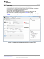
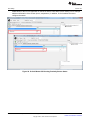
Follow the steps of the IO-Link Master’s user’s manual to connect to it and import the IODD.
After the connection is established, the screen shown in Figure 24 will be visible.
The tab Process Data is showing if the Hall Effect sensor is switched on (TRUE) or not (FALSE). See
Figure 25.
Figure 25. IO-Link Master GUI After Established Connection to TI's IO-Link Device
TIDU671 – March 2015
Submit Documentation Feedback
Hall-Effect Proximity Sensor With IO-Link™ Design Guide
Copyright © 2015, Texas Instruments Incorporated
23
Test Setup
www.ti.com
Modifications of the IO-Link application on the MCU and the IODD allow to also reading out for example
additional information of the sensor (that is, temperature). In addition, IO-Link enables the user to
configure the sensor.
Figure 26. IO-Link Master GUI Showing Proximity Sensor Status
24
Hall-Effect Proximity Sensor With IO-Link™ Design Guide
Copyright © 2015, Texas Instruments Incorporated
TIDU671 – March 2015
Submit Documentation Feedback
Test Results
www.ti.com
5
Test Results
5.1
Power Consumption in SIO Mode
The power consumption of the system is plotted in Figure 27, where the L+ voltage was varied between
18 and 33 V.
Two curves are visible: one when the LED was ‘OFF’ (equivalent to the field has been below BOPof
DRV5013) and LED ‘ON’ (when the field has been above BRP).
8
7.5
Y Axis Title (?)
7
6.5
6
5.5
5
4.5
LED ON
LED OFF
4
18
20
22
24
26
Vin
28
30
32
34
D001
Figure 27. Power Consumption
5.2
BxP Distributions
Following the test procedure detailed in Section 4.3 gives the following plots.
Given the size of the sample set (80 values), the standard deviation can be considered a good estimate of
the random variable being observed.
40
35
F re q u e n cy
30
20
20
10
0
1.78
1.89
3
2
1
0
2
0
1.99
2.10
2.20
2.31
2.41
2.52
Bin
2.63
More
D001
Figure 28. BOP Histogram
Given the sample size, the average for the TIDA-00340 at 25°C for BOP is
µ BOP = 2.09 ± 6.6 ´ 1/ 80 ~ 2.09 ± 0.7 mT
TIDU671 – March 2015
Submit Documentation Feedback
(1)
Hall-Effect Proximity Sensor With IO-Link™ Design Guide
Copyright © 2015, Texas Instruments Incorporated
25
Test Results
www.ti.com
40
30
F re q u e n cy
26
22
20
10
7
6
2
0
0
1.40
0
1.59
1.79
1.99
2.18
2.38
2.57
0
2.77
2.96
More
Bin
D002
Figure 29. BRP Histogram
µ BRP = 1.99 ± 6.6 ´ 1/ 80 ~ 1.99 ± 0.7 mT
(2)
40
29
F re q u e n cy
30
20
20
9
10
5
0
0
-0.73
0
-0.45
0
-0.17
0.11
0.39
0.67
0
0.95
1.23
Bin
1.51
More
D003
Figure 30. BOP - BRP
The mismatch between BRP and BOP is
µ Delta = 0.11 ± 0.7 mT
26
Hall-Effect Proximity Sensor With IO-Link™ Design Guide
Copyright © 2015, Texas Instruments Incorporated
(3)
TIDU671 – March 2015
Submit Documentation Feedback
Test Results
www.ti.com
5.3
BxP versus L+ Supply Voltage
The standard deviation for the BxP values is 0.04 for BOP and 0.06 for BRP. So, the variations that are
observed are well within the ±3 σ, and resultantly no correlation between the operating or releasing fields
and the system supply voltage can be seen.
2.20
BOP_av
BRP_av
2.15
B xP V a lu e s
2.10
2.05
2.00
1.95
1.90
10
15
20
L+ Voltage
25
30
33
D004
Figure 31. BxP Values versus L+
5.4
Power Consumption in IO-Link Mode
Under standard condition, voltage of the L+ is 24 V. With the current at 7.5 mA and LED ON, the power
consumption is 9.4 mA.
TIDU671 – March 2015
Submit Documentation Feedback
Hall-Effect Proximity Sensor With IO-Link™ Design Guide
Copyright © 2015, Texas Instruments Incorporated
27
Design Files
www.ti.com
6
Design Files
6.1
Schematics
To download the schematics, see the design files at TIDA-00340.
VCC
VCC
R1
10.0k
U1
1
VCC
OUT
GND
R2
2
HALL_OUT
0
3
DRV5013ADQDBZ
C2
0.022µF
C1
680pF
GND
2
RF071M2S
1
C3
4.7µF
820
U2
Green
8
7
1
U3
SW
HALL_OUT
PWR_OK
TEMP_OK
WAKE
CUR_OK
HALL_OUT
VCC
1
2
3
4
5
6
16
17
P1.0/TA0.1/DMAE0/RTCCLK/A0/CD0/VEREFP1.1/TA0.2/TA1CLK/CDOUT/A1/CD1/VEREF+
P1.2/TA1.1/TA0CLK/CDOUT/A2/CD2
P1.3/TA1.2/UCB0STE/A3/CD3
P1.4/TB0.1/UCA0STE/A4/CD4
P1.5/TB0.2/UCA0CLK/A5/CD5
P1.6/UCB0SIMO/UCB0SDA/TA0.0
P1.7/UCB0SOMI/UCB0SCL/TA1.0
VCC
18
24
20
GND
P2.0/UCA0TXD/UCA0SIMO/TB0CLK/ACLK
P2.1/UCA0RXD/UCA0SOMI/TB0.0
P2.2/UCB0CLK
PJ.0/TDO/TB0OUTH/SMCLK/CD6
PJ.1/TDI/TCLK/MCLK/CD7
PJ.2/TMS/ACLK/CD8
PJ.3/TCK/CD9
PJ.4/XIN
PJ.5/XOUT
RST/NMI/SBWTDIO
TEST/SBWTCK
VCORE
QFN PAD
AVSS
DVSS
AVCC
DVCC
13
14
15
7
8
9
10
21
22
Tx
Rx
18
20
17
EN
5
15
19
16
R7
47k
12
11
25
23
19
C8
2200pF
VCC
VCC
J2
4
3
2
1
C4 DNPC5
2.2µF
330pF
4
VCCOUT
VCCIN
L+
VCCSET
CQ
TX
EN
RX
PWR_OK
CUR_OK
TEMP_OK
WAKE
ILIM_ADJ
LGND
GND
GND
PAD
NC
NC
NC
10
D4
30V
C6
0.1µF
D5
1
R6
L+
2
GND
VCC
30V
J1
09 0431 212 04
12
CQ
14
3
6
13
C7
330pF
D6
4
S1
GND
D2
1
Yellow
D3
3
1
D1
2
820
SMAJ30CA
2
R5
SMAJ30CA
GND
GND
SMAJ30CA
GND
30V
2
11
9
SN65HVD101RGB
R8
4.7k
GND
MSP430FR5738IRGE
GND
C9
0.47µF
GND
C10
0.1µF
GND
C11
0.1µF
C12
4.7µF
GND
GND
GND
Figure 32. Hall-Effect Proximity Sensor With IO-Link Schematic
space
space
28
Hall-Effect Proximity Sensor With IO-Link™ Design Guide
TIDU671 – March 2015
Submit Documentation Feedback
Copyright © 2015, Texas Instruments Incorporated
Design Files
www.ti.com
6.2
Bill of Materials
To download the bill of materials (BOM), see the design files at TIDA-00340.
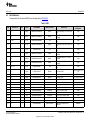
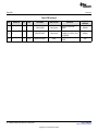
Table 4. BOM
ITEM
DESIGNATOR
QTY
VALUE
PARTNUMBER
MANUFACTURER
DESCRIPTION
PACKAGE
REFERENCE
1
C1
1
680 pF
GRM155R71H681KA01D
Murata
CAP, CERM, 680 pF, 50 V, ±10%, X7R,
0402
0402
2
C2
1
0.022 µF
GRM155R71C223KA01D
Murata
CAP, CERM, 0.022 µF, 16 V, ±10%,
X7R, 0402
0402
3
C3, C12
2
4.7 µF
C1005X5R0J475M050BC
TDK
CAP, CERM, 4.7 µF, 6.3 V, ±20%, X5R,
0402
0402
4
C4
1
2.2 µF
GRM32ER72A225KA35L
Murata
CAP, CERM, 2.2 µF, 100 V, ±10%, X7R,
1210
1210
5
C6
1
0.1 µF
12061C104JAT2A
AVX
CAP, CERM, 0.1 µF, 100 V, ±5%, X7R,
1206
1206
6
C7
1
330 pF
GRM155R72A331KA01D
Murata
CAP, CERM, 330 pF, 100 V, ±10%,
X7R, 0402
0402
7
C8
1
2200 pF
GRM155R70J222KA01D
Murata
CAP, CERM, 2200 pF, 6.3 V, ±10%,
X7R, 0402
0402
8
C9
1
0.47 µF
GRM155R60J474KE19D
Murata
CAP, CERM, 0.47 µF, 6.3 V, ±10%,
X5R, 0402
0402
9
C10, C11
2
0.1 µF
C1005X5R0J104K
TDK
CAP, CERM, 0.1 µF, 6.3 V, ±10%, X5R,
0402
0402
10
D1
1
Yellow
LY L29K-J1K2-26-Z
OSRAM
11
D2
1
200 V
RF071M2S
Rohm
12
D3
1
Green
LG L29K-G2J1-24-Z
OSRAM
LED, Green, SMD
13
D4, D5, D6
3
30 V
SMAJ30CA
Bourns
Diode, TVS, Bi, 30 V, 400 W, SMA
14
J1
1
09 0431 212 04
Binder-Connector
15
J2
1
850-10-004-40-001000
Mill-Max
16
R1
1
CRCW040210K0FKED
Vishay-Dale
RES, 10.0 kΩ, 1%, 0.063 W, 0402
0402
17
R2
1
0
CRCW04020000Z0ED
Vishay-Dale
RES, 0, 5%, 0.063 W, 0402
0402
18
R5, R6
2
820
CRCW0402820RJNED
Vishay-Dale
RES, 820 Ω, 5%, 0.063W, 0402
0402
19
R7
1
47 k
CRCW040247K0JNED
Vishay-Dale
RES, 47 kΩ, 5%, 0.063 W, 0402
0402
20
R8
1
4.7k
CRCW04024K70JNED
Vishay-Dale
RES, 4.7 kΩ, 5%, 0.063 W, 0402
21
S1
1
SKRKAEE010
Alps
22
U1
1
DRV5013ADQDBZ
Texas Instruments
10.0 k
TIDU671 – March 2015
Submit Documentation Feedback
LED, Yellow, SMD
Diode, Ultrafast, 200 V, 1 A, SOD-123
M12 Socket, 4Pos, TH
Header, 4×1, 50 mil, R/A, SMT
Switch, Push Button, SMD
Digital-Latch Hall Effect Sensor,
DBZ0003A
LED, 1.3 × 0.65 × 0.8
mm
SOD-123
1.7 × 0.65 × 0.8 mm
SMA
M12 Conn D12×14.3
Header, 50 mil, R/A,SMT
0402
2.9×2×3.9-mm SMD
DBZ0003A
Hall-Effect Proximity Sensor With IO-Link™ Design Guide
Copyright © 2015, Texas Instruments Incorporated
29
Design Files
www.ti.com
Table 4. BOM (continued)
ITEM
30
DESIGNATOR
QTY
VALUE
PARTNUMBER
MANUFACTURER
PACKAGE
REFERENCE
DESCRIPTION
23
U2
1
SN65HVD101RGB
Texas Instruments
IO-Link PHY for Device Nodes,
RGB0020A
RGB0020A
24
U3
1
MSP430FR5738IRGE
Texas Instruments
24-MHz Mixed Signal Microcontroller,
1024 B SRAM and 17 GPIOs, –40°C to
85°C, RGE0024G
RGE0024G
25
C5
0
GRM155R72A331KA01D
Murata
330 pF
Hall-Effect Proximity Sensor With IO-Link™ Design Guide
CAP, CERM, 330 pF, 100 V, ±10%,
X7R, 0402
0402
TIDU671 – March 2015
Submit Documentation Feedback
Copyright © 2015, Texas Instruments Incorporated
Design Files
www.ti.com
6.3
Layer Plots
To download the layer plots, see the design files at TIDA-00340.
6.4
Figure 33. Top Overlay
Figure 34. Top Solder
Figure 35. Top Layer
Figure 36. Mid Layer 1
Figure 37. Mid Layer 2
Figure 38. Bottom Layer
Figure 39. Bottom Solder
Figure 40. Bottom Overlay
Figure 41. Drill Drawing
Figure 42. Board Dimensions
Altium Project
To download the Altium project files, see the design files at TIDA-00340.
6.5
Gerber Files
To download the Gerber files, see the design files at TIDA-00340.
TIDU671 – March 2015
Submit Documentation Feedback
Hall-Effect Proximity Sensor With IO-Link™ Design Guide
Copyright © 2015, Texas Instruments Incorporated
31
Design Files
6.6
www.ti.com
Assembly Drawings
Figure 43. Top Assembly Drawing
6.7
Figure 44. Bottom Assembly Drawing
Software Files
To download the software files, see the design files at TIDA-00340.
7
References
1. IO-Link Interface and System Specification v1.1.2, IO-Link Community (PDF)
2. IO-Link Test Specification v1.1, IO-Link Community (PDF)
3. Reliability of Ferroelectric Random Access Memory Embedded within 130 nm CMOS, J. Rodriguez, K.
Remack, J. Gertas, L. Wang, C. Zhou, K. Boku, J. Rodriguez-Latorre, Reliability Physics Symposium
(IRPS), 2010 IEEE International
4. IEC60947-5-2:2007, Low-voltage switchgear and controlgear – Part 5-2: Control circuit devices and
switching elements – Proximity switches, IEC2007
5. IEC 61131-2, Programmable Controllers – Part 2: Equipment Requirements and Tests, IEC Webstore
(http://webstore.iec.ch/webstore/webstore.nsf/artnum/046361!opendocument)
6. Advanced Debugging Using the Enhanced Emulation Module, (SLAA393)
7. E. Ramsden, Hall-Effect Sensors: Theory and Application, Second Edition, Newnes, 2006.
8
About the Author
MATTHIEU CHEVRIER is a systems architect at Texas Instruments, where he is responsible for defining
and developing reference design solutions for the industrial segment. Matthieu brings to this role his
extensive experience in embedded system designs in both hardware (power management, mixed signal,
and so on) and software (such as low level drivers, RTOS, and compilers). Matthieu earned his master of
science in electrical engineering (MSEE) from Supélec, an Ivy League university in France. Matthieu holds
patents from IPO, EPO, and USPTO.
ALEXANDER WEILER is a systems architect at Texas Instruments, where he is responsible for
developing reference design solutions for the industrial segment. Alexander brings to this role his
extensive experience in high-speed digital, low-noise analog, and RF system-level design expertise.
Alexander earned his diploma in electrical engineering (Dipl.-Ing. (FH)) from the University of Applied
Science in Karlsruhe, Germany.
32
Hall-Effect Proximity Sensor With IO-Link™ Design Guide
Copyright © 2015, Texas Instruments Incorporated
TIDU671 – March 2015
Submit Documentation Feedback
IMPORTANT NOTICE FOR TI REFERENCE DESIGNS
Texas Instruments Incorporated ("TI") reference designs are solely intended to assist designers (“Buyers”) who are developing systems that
incorporate TI semiconductor products (also referred to herein as “components”). Buyer understands and agrees that Buyer remains
responsible for using its independent analysis, evaluation and judgment in designing Buyer’s systems and products.
TI reference designs have been created using standard laboratory conditions and engineering practices. TI has not conducted any
testing other than that specifically described in the published documentation for a particular reference design. TI may make
corrections, enhancements, improvements and other changes to its reference designs.
Buyers are authorized to use TI reference designs with the TI component(s) identified in each particular reference design and to modify the
reference design in the development of their end products. HOWEVER, NO OTHER LICENSE, EXPRESS OR IMPLIED, BY ESTOPPEL
OR OTHERWISE TO ANY OTHER TI INTELLECTUAL PROPERTY RIGHT, AND NO LICENSE TO ANY THIRD PARTY TECHNOLOGY
OR INTELLECTUAL PROPERTY RIGHT, IS GRANTED HEREIN, including but not limited to any patent right, copyright, mask work right,
or other intellectual property right relating to any combination, machine, or process in which TI components or services are used.
Information published by TI regarding third-party products or services does not constitute a license to use such products or services, or a
warranty or endorsement thereof. Use of such information may require a license from a third party under the patents or other intellectual
property of the third party, or a license from TI under the patents or other intellectual property of TI.
TI REFERENCE DESIGNS ARE PROVIDED "AS IS". TI MAKES NO WARRANTIES OR REPRESENTATIONS WITH REGARD TO THE
REFERENCE DESIGNS OR USE OF THE REFERENCE DESIGNS, EXPRESS, IMPLIED OR STATUTORY, INCLUDING ACCURACY OR
COMPLETENESS. TI DISCLAIMS ANY WARRANTY OF TITLE AND ANY IMPLIED WARRANTIES OF MERCHANTABILITY, FITNESS
FOR A PARTICULAR PURPOSE, QUIET ENJOYMENT, QUIET POSSESSION, AND NON-INFRINGEMENT OF ANY THIRD PARTY
INTELLECTUAL PROPERTY RIGHTS WITH REGARD TO TI REFERENCE DESIGNS OR USE THEREOF. TI SHALL NOT BE LIABLE
FOR AND SHALL NOT DEFEND OR INDEMNIFY BUYERS AGAINST ANY THIRD PARTY INFRINGEMENT CLAIM THAT RELATES TO
OR IS BASED ON A COMBINATION OF COMPONENTS PROVIDED IN A TI REFERENCE DESIGN. IN NO EVENT SHALL TI BE
LIABLE FOR ANY ACTUAL, SPECIAL, INCIDENTAL, CONSEQUENTIAL OR INDIRECT DAMAGES, HOWEVER CAUSED, ON ANY
THEORY OF LIABILITY AND WHETHER OR NOT TI HAS BEEN ADVISED OF THE POSSIBILITY OF SUCH DAMAGES, ARISING IN
ANY WAY OUT OF TI REFERENCE DESIGNS OR BUYER’S USE OF TI REFERENCE DESIGNS.
TI reserves the right to make corrections, enhancements, improvements and other changes to its semiconductor products and services per
JESD46, latest issue, and to discontinue any product or service per JESD48, latest issue. Buyers should obtain the latest relevant
information before placing orders and should verify that such information is current and complete. All semiconductor products are sold
subject to TI’s terms and conditions of sale supplied at the time of order acknowledgment.
TI warrants performance of its components to the specifications applicable at the time of sale, in accordance with the warranty in TI’s terms
and conditions of sale of semiconductor products. Testing and other quality control techniques for TI components are used to the extent TI
deems necessary to support this warranty. Except where mandated by applicable law, testing of all parameters of each component is not
necessarily performed.
TI assumes no liability for applications assistance or the design of Buyers’ products. Buyers are responsible for their products and
applications using TI components. To minimize the risks associated with Buyers’ products and applications, Buyers should provide
adequate design and operating safeguards.
Reproduction of significant portions of TI information in TI data books, data sheets or reference designs is permissible only if reproduction is
without alteration and is accompanied by all associated warranties, conditions, limitations, and notices. TI is not responsible or liable for
such altered documentation. Information of third parties may be subject to additional restrictions.
Buyer acknowledges and agrees that it is solely responsible for compliance with all legal, regulatory and safety-related requirements
concerning its products, and any use of TI components in its applications, notwithstanding any applications-related information or support
that may be provided by TI. Buyer represents and agrees that it has all the necessary expertise to create and implement safeguards that
anticipate dangerous failures, monitor failures and their consequences, lessen the likelihood of dangerous failures and take appropriate
remedial actions. Buyer will fully indemnify TI and its representatives against any damages arising out of the use of any TI components in
Buyer’s safety-critical applications.
In some cases, TI components may be promoted specifically to facilitate safety-related applications. With such components, TI’s goal is to
help enable customers to design and create their own end-product solutions that meet applicable functional safety standards and
requirements. Nonetheless, such components are subject to these terms.
No TI components are authorized for use in FDA Class III (or similar life-critical medical equipment) unless authorized officers of the parties
have executed an agreement specifically governing such use.
Only those TI components that TI has specifically designated as military grade or “enhanced plastic” are designed and intended for use in
military/aerospace applications or environments. Buyer acknowledges and agrees that any military or aerospace use of TI components that
have not been so designated is solely at Buyer's risk, and Buyer is solely responsible for compliance with all legal and regulatory
requirements in connection with such use.
TI has specifically designated certain components as meeting ISO/TS16949 requirements, mainly for automotive use. In any case of use of
non-designated products, TI will not be responsible for any failure to meet ISO/TS16949.IMPORTANT NOTICE
Mailing Address: Texas Instruments, Post Office Box 655303, Dallas, Texas 75265
Copyright © 2015, Texas Instruments Incorporated