1
20P506-00 E4 – 2014-01-15
User Manual
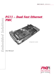
P506 – Quad CAN Bus
Interface PMC
Configuration example
P506 - Quad CAN Bus Interface PMC
P506 - Quad CAN Bus Interface PMC
The P506 is a 32-bit/33MHz PMC with four CAN interfaces. They support CAN
Protocol Version 2.0A/B, standard and extended data frames, remote frames, 0..8
bytes data length and a programmable data rate of up to 1 Mbit/s.
The P506 is based on the USM™ concept. USM™ Universal Submodules make
PMC modules more flexible than ever. The CAN bus interfaces are realized via four
IP cores implemented inside its onboard FPGA. This function can be changed at any
time through implementation of different IP cores. The corresponding line drivers
are realized on the USM™ which is simply plugged on the P506.
The I/O mezzanine module is suitable for any PMC compliant host carrier board in
any type of bus system, i.e. CPCI, VME or on any type of stand-alone SBC in
telecommunication, industrial, medical, transportation or aerospace applications. It
offers long-term availability for at least 10 years and is qualified for operation in the
extended temperature range.
MEN Mikro Elektronik GmbH
20P506-00 E4 – 2014-01-15
2
Diagram
Diagram
U SM
5 0 ‐p in F ro n t C o n n e c to r
4 Iso la te d C A N In te rfa c e s
MEN Mikro Elektronik GmbH
20P506-00 E4 – 2014-01-15
FPGA
CAN C o n tro lle rs
PCI
In te rfa ce
P C I In te rfa c e
3 2 ‐b it /
3 3 ‐M H z
3
Technical Data
Technical Data
CAN Interface
• Compliant to ISO 11898-1 and ISO 11898-2
• Four channels
• CAN Protocol Version 2.0A/B
- Standard and extended data frames
- 0..8 bytes data length
- Programmable data rate up to 1 Mbit/s
• Support for remote frames
• 5 receive buffers (FIFO-scheme)
• 3 transmit buffers with prioritization
• Maskable identifier filter
• Programmable loop-back mode for self-test operation
• Signaling and interrupt capabilities for receiver and transmitter error states
Memory
• 32MB SDRAM memory
- Soldered
- DDR2
- 132MHz memory bus frequency
- FPGA-controlled
• 2MB non-volatile Flash
- For FPGA data and Nios® firmware
- FPGA-controlled
FPGA
• Standard factory FPGA configuration:
- Main bus interface
- Interrupt controller, SMBus controller
- 16Z029_CAN – CAN Controller
- 16Z043_SDRAM – SDRAM controller
- 16Z045_FLASH – Flash interface
- 16Z034_GPIO – GPIO controller
- 16Z034_PWM – PWM Pulse Width Modulation
• The FPGA offers the possibility to add customized I/O functionality. See FPGA.
PMC Characteristics (PCI)
• Compliant with PCI Specification 2.2
• 32-bit/33-MHz, 3.3V V(I/O)
• Target
Peripheral Connections
• Via front panel on a shielded 50-pin HP D-Sub SCSI 2 receptacle connector
MEN Mikro Elektronik GmbH
20P506-00 E4 – 2014-01-15
4
Technical Data
Electrical Specifications
• Isolation voltage:
- 500 VAC
• Supply voltage/power consumption:
- +5V (-3%/+5%), 240mA
- +3.3V (-5%/+5%), 15mA
Mechanical Specifications
• Dimensions: conforming to IEEE 1386.1
• Weight: 78g
Environmental Specifications
• Temperature range (operation):
- -40..+85°C (qualified components)
- Airflow: min. 1.0m/s
• Temperature range (storage): -40..+85°C
• Relative humidity (operation): max. 95% non-condensing
• Relative humidity (storage): max. 95% non-condensing
• Altitude: -300m to + 3,000m
• Shock: 15g/11ms
• Bump: 10g/16ms
• Vibration (sinusoidal): 1g/10..150Hz
• Conformal coating on request
MTBF
• 957 834 h @ 40°C according to IEC/TR 62380 (RDF 2000)
Safety
• PCB manufactured with a flammability rating of 94V-0 by UL recognized manufacturers
EMC
• Conforming to EN 55022 (radio disturbance), IEC1000-4-2 (ESD) and
IEC1000-4-4 (burst)
Software Support
•
•
•
•
•
Windows®
Linux
VxWorks®
QNX®
For more information on supported operating system versions and drivers see
online data sheet.
MEN Mikro Elektronik GmbH
20P506-00 E4 – 2014-01-15
5
Configuration Options
Configuration Options
CPU
• Nios® soft core implementation possible (e.g. for real-time Ethernet)
Rear I/O
• Via Pn4 rear I/O connector
Cooling
• Conduction Cooling
Please note that some of these options may only be available for large
volumes. Please ask our sales staff for more information.
For available standard configurations see online data sheet.
MEN Mikro Elektronik GmbH
20P506-00 E4 – 2014-01-15
6
FPGA
FPGA
Flexible Configuration
• Customized I/O functions can be added to the FPGA.
• It depends on the board type, pin counts and number of logic elements which IP
cores make sense and/or can be implemented. Please contact MEN for information on feasibility.
• You can find more information on our web page "User I/O in FPGA"
FPGA Capabilities
• FPGA Altera® Cyclone® II EP2C35
- 33,216 logic elements
- 483,840 total RAM bits
- Supports Nios® II soft processor
• Connection
- Functions can be linked to Wishbone or Avalon® bus
- Available pin count: 46 pins (FPGA to USM™)
- Functions available via USM™ at front I/O connector
• MEN offers a USM™ development kit and an FPGA Development Package as
well as Flash update tools for different operating systems.
MEN Mikro Elektronik GmbH
20P506-00 E4 – 2014-01-15
7
Product Safety
Product Safety
!
Electrostatic Discharge (ESD)
Computer boards and components contain electrostatic sensitive devices.
Electrostatic discharge (ESD) can damage components. To protect the board and
other components against damage from static electricity, you should follow some
precautions whenever you work on your computer.
• Power down and unplug your computer system when working on the inside.
• Hold components by the edges and try not to touch the IC chips, leads, or circuitry.
• Use a grounded wrist strap before handling computer components.
• Place components on a grounded antistatic pad or on the bag that came with the
component whenever the components are separated from the system.
• Store the board only in its original ESD-protected packaging. Retain the original
packaging in case you need to return the board to MEN for repair.
MEN Mikro Elektronik GmbH
20P506-00 E4 – 2014-01-15
8
About this Document
About this Document
This user manual is intended only for system developers and integrators, it is not
intended for end users.
It describes the hardware functions of the board, connection of peripheral devices
and integration into a system. It also provides additional information for special
applications and configurations of the board.
The manual does not include detailed information on individual components (data
sheets etc.). A list of literature is given in the appendix.
History
Issue
Date
E1
First issue
2009-06-15
E2
Corrected Table 6, Register values for switching on
the CAN interfaces, on page 26
2009-10-19
E3
Corrected isolation voltage, added GPIO2 and recommended cables
2013-03-08
E4
Removed GPIO2
2014-01-15
MEN Mikro Elektronik GmbH
20P506-00 E4 – 2014-01-15
Comments
9
About this Document
Conventions
This sign marks important notes or warnings concerning the use of voltages which
can lead to serious damage to your health and also cause damage or destruction of
the component.
!
italics
bold
monospace
This sign marks important notes or warnings concerning proper functionality of the
product described in this document. You should read them in any case.
Folder, file and function names are printed in italics.
Bold type is used for emphasis.
A monospaced font type is used for hexadecimal numbers, listings, C function
descriptions or wherever appropriate. Hexadecimal numbers are preceded by "0x".
comment
Comments embedded into coding examples are shown in green color.
hyperlink
Hyperlinks are printed in blue color.
The globe will show you where hyperlinks lead directly to the Internet, so you can
look for the latest information online.
IRQ#
/IRQ
Signal names followed by "#" or preceded by a slash ("/") indicate that this signal is
either active low or that it becomes active at a falling edge.
in/out
Signal directions in signal mnemonics tables generally refer to the corresponding
board or component, "in" meaning "to the board or component", "out" meaning
"coming from it".
Vertical lines on the outer margin signal technical changes to the previous issue of
the document.
MEN Mikro Elektronik GmbH
20P506-00 E4 – 2014-01-15
10
About this Document
Legal Information
Changes
MEN Mikro Elektronik GmbH ("MEN") reserves the right to make changes without further notice to any products
herein.
Warranty, Guarantee, Liability
MEN makes no warranty, representation or guarantee of any kind regarding the suitability of its products for any
particular purpose, nor does MEN assume any liability arising out of the application or use of any product or
circuit, and specifically disclaims any and all liability, including, without limitation, consequential or incidental
damages. TO THE EXTENT APPLICABLE, SPECIFICALLY EXCLUDED ARE ANY IMPLIED
WARRANTIES ARISING BY OPERATION OF LAW, CUSTOM OR USAGE, INCLUDING WITHOUT
LIMITATION, THE IMPLIED WARRANTIES OF MERCHANTABILITY AND FITNESS FOR A
PARTICULAR PURPOSE OR USE. In no event shall MEN be liable for more than the contract price for the
products in question. If buyer does not notify MEN in writing within the foregoing warranty period, MEN shall
have no liability or obligation to buyer hereunder.
The publication is provided on the terms and understanding that:
1. MEN is not responsible for the results of any actions taken on the basis of information in the publication, nor
for any error in or omission from the publication; and
2. MEN is not engaged in rendering technical or other advice or services.
MEN expressly disclaims all and any liability and responsibility to any person, whether a reader of the publication
or not, in respect of anything, and of the consequences of anything, done or omitted to be done by any such person
in reliance, whether wholly or partially, on the whole or any part of the contents of the publication.
Conditions for Use, Field of Application
The correct function of MEN products in mission-critical and life-critical applications is limited to the
environmental specification given for each product in the technical user manual. The correct function of MEN
products under extended environmental conditions is limited to the individual requirement specification and
subsequent validation documents for each product for the applicable use case and has to be agreed upon in writing
by MEN and the customer. Should the customer purchase or use MEN products for any unintended or
unauthorized application, the customer shall indemnify and hold MEN and its officers, employees, subsidiaries,
affiliates, and distributors harmless against all claims, costs, damages, and expenses, and reasonable attorney fees
arising out of, directly or indirectly, any claim or personal injury or death associated with such unintended or
unauthorized use, even if such claim alleges that MEN was negligent regarding the design or manufacture of the
part. In no case is MEN liable for the correct function of the technical installation where MEN products are a part
of.
Trademarks
All products or services mentioned in this publication are identified by the trademarks, service marks, or product
names as designated by the companies which market those products. The trademarks and registered trademarks
are held by the companies producing them. Inquiries concerning such trademarks should be made directly to those
companies.
Conformity
MEN products are no ready-made products for end users. They are tested according to the standards given in the
Technical Data and thus enable you to achieve certification of the product according to the standards applicable in
your field of application.
MEN Mikro Elektronik GmbH
20P506-00 E4 – 2014-01-15
11
About this Document
RoHS
Since July 1, 2006 all MEN standard products comply with RoHS legislation.
Since January 2005 the SMD and manual soldering processes at MEN have already been completely lead-free.
Between June 2004 and June 30, 2006 MEN’s selected component suppliers have changed delivery to RoHScompliant parts. During this period any change and status was traceable through the MEN ERP system and the
boards gradually became RoHS-compliant.
WEEE Application
The WEEE directive does not apply to fixed industrial plants and tools. The compliance is the responsibility of the
company which puts the product on the market, as defined in the directive; components and sub-assemblies are
not subject to product compliance.
In other words: Since MEN does not deliver ready-made products to end users, the WEEE directive is not
applicable for MEN. Users are nevertheless recommended to properly recycle all electronic boards which have
passed their life cycle.
Nevertheless, MEN is registered as a manufacturer in Germany. The registration number can be provided on
request.
Copyright © 2014 MEN Mikro Elektronik GmbH. All rights reserved.
Germany
MEN Mikro Elektronik GmbH
Neuwieder Straße 3-7
90411 Nuremberg
Phone +49-911-99 33 5-0
Fax +49-911-99 33 5-901
E-mail [email protected]
www.men.de
MEN Mikro Elektronik GmbH
20P506-00 E4 – 2014-01-15
France
MEN Mikro Elektronik SA
18, rue René Cassin
ZA de la Châtelaine
74240 Gaillard
Phone +33 (0) 450-955-312
Fax +33 (0) 450-955-211
E-mail [email protected]
www.men-france.fr
USA
MEN Micro Inc.
860 Penllyn Blue Bell Pike
Blue Bell, PA 19422
Phone (215) 542-9575
Fax (215) 542-9577
E-mail [email protected]
www.menmicro.com
12
Contents
Contents
1 Getting Started . . . . . . . . . . . . . . . . . . . . . . . . . . . . . . . . . . . . . . . . . . . . . . . .
1.1 Map of the Board. . . . . . . . . . . . . . . . . . . . . . . . . . . . . . . . . . . . . . . . .
1.2 Integrating the Board into a System . . . . . . . . . . . . . . . . . . . . . . . . . .
1.3 Installing Driver Software . . . . . . . . . . . . . . . . . . . . . . . . . . . . . . . . . .
1.4 Switching on the CAN Interfaces . . . . . . . . . . . . . . . . . . . . . . . . . . . .
16
16
17
17
17
2 Connecting the PMC Module . . . . . . . . . . . . . . . . . . . . . . . . . . . . . . . . . . . .
2.1 Peripheral Interfaces . . . . . . . . . . . . . . . . . . . . . . . . . . . . . . . . . . . . . .
2.1.1
Standard Version . . . . . . . . . . . . . . . . . . . . . . . . . . . . . . . . . .
2.1.2
Conduction Cooled Version (Optional). . . . . . . . . . . . . . . . .
2.2 Host PCI Interface . . . . . . . . . . . . . . . . . . . . . . . . . . . . . . . . . . . . . . . .
18
18
18
20
23
3 Functional Description . . . . . . . . . . . . . . . . . . . . . . . . . . . . . . . . . . . . . . . . . .
3.1 Power Supply. . . . . . . . . . . . . . . . . . . . . . . . . . . . . . . . . . . . . . . . . . . .
3.2 Memory . . . . . . . . . . . . . . . . . . . . . . . . . . . . . . . . . . . . . . . . . . . . . . . .
3.2.1
DRAM System Memory . . . . . . . . . . . . . . . . . . . . . . . . . . . .
3.2.2
Flash . . . . . . . . . . . . . . . . . . . . . . . . . . . . . . . . . . . . . . . . . . .
3.3 CAN Interfaces . . . . . . . . . . . . . . . . . . . . . . . . . . . . . . . . . . . . . . . . . .
3.3.1
Activating the Termination Resistors . . . . . . . . . . . . . . . . . .
3.3.2
Switching on the Interfaces. . . . . . . . . . . . . . . . . . . . . . . . . .
25
25
25
25
25
25
25
26
4 FPGA . . . . . . . . . . . . . . . . . . . . . . . . . . . . . . . . . . . . . . . . . . . . . . . . . . . . . . . . 28
4.1 FPGA Configuration Table . . . . . . . . . . . . . . . . . . . . . . . . . . . . . . . . . 29
5 Appendix . . . . . . . . . . . . . . . . . . . . . . . . . . . . . . . . . . . . . . . . . . . . . . . . . . . . .
5.1 PCI Configuration . . . . . . . . . . . . . . . . . . . . . . . . . . . . . . . . . . . . . . . .
5.2 Literature and Web Resources . . . . . . . . . . . . . . . . . . . . . . . . . . . . . . .
5.2.1
CAN Bus . . . . . . . . . . . . . . . . . . . . . . . . . . . . . . . . . . . . . . . .
5.3 Finding out the Board’s Article Number, Revision
and Serial Number . . . . . . . . . . . . . . . . . . . . . . . . . . . . . . . . . . . . . . . .
MEN Mikro Elektronik GmbH
20P506-00 E4 – 2014-01-15
30
30
30
30
30
13
Figures
Figure 1.
Figure 2.
Figure 3.
Figure 4.
MEN Mikro Elektronik GmbH
20P506-00 E4 – 2014-01-15
Map of the board – top view (standard version). . . . . . . . . . . . . . . . . .
Map of the board – top view (conduction cooled version). . . . . . . . . .
Block Diagram . . . . . . . . . . . . . . . . . . . . . . . . . . . . . . . . . . . . . . . . . . .
Label giving the board’s article number, revision and serial number .
16
16
29
30
14
Tables
Table 1.
Table 2.
Table 3.
Table 4.
Table 5.
Table 6.
Table 7.
Table 8.
MEN Mikro Elektronik GmbH
20P506-00 E4 – 2014-01-15
Pin assignment of 50-pin HP D-Sub front connector . . . . . . . . . . . . . .
Pin assignment of 64-pin plug connector Pn4 . . . . . . . . . . . . . . . . . . .
Signal mnemonics. . . . . . . . . . . . . . . . . . . . . . . . . . . . . . . . . . . . . . . . .
Pin assignment of 64-pin board-to-board connector Pn1 . . . . . . . . . . .
Pin assignment of 64-pin board-to-board connector Pn2 . . . . . . . . . . .
Register values for switching on the CAN interfaces. . . . . . . . . . . . . .
Correspondence between MDIS API functions and low-level driver
functions . . . . . . . . . . . . . . . . . . . . . . . . . . . . . . . . . . . . . . . . . . . . . . . .
FPGA – Factory standard configuration table for P506 . . . . . . . . . . . .
19
21
21
23
24
26
26
29
15
Getting Started
1
Getting Started
This chapter gives an overview of the board and some hints for first installation in a
system.
1.1
Map of the Board
Figure 1. Map of the board – top view (standard version)
FPGA
50-pin
HP D-Sub
SCSI 2
connector
PCI bus
connectors
Pn1
Pn2
USM
Figure 2. Map of the board – top view (conduction cooled version)
Secondary thermal interface
USM
Primary thermal interface
Primary thermal interface
Pn4
FPGA
PCI bus
connectors
Pn1
Pn2
Secondary thermal interface
MEN Mikro Elektronik GmbH
20P506-00 E4 – 2014-01-15
16
Getting Started
1.2
Integrating the Board into a System
You can use the following "check list" to install the PMC on a carrier board for the
first time and to test proper functioning of the board.
Power-down the system and remove the PMC carrier board.
Install the PMC in a suitable front-panel slot of the carrier board as described in
the carrier board’s user manual.
Insert the carrier board into the system again.
Power-up the system.
If there is a system crash or other abnormal behavior at start-up, check if the
PMC is plugged properly.
You can now install driver software for the P506.
1.3
Installing Driver Software
For a detailed description on how to install driver software please refer to the
respective documentation.
You can find any driver software available for download on MEN’s website.
1.4
Switching on the CAN Interfaces
The CAN interfaces have to be switched on individually. See Chapter 3.3.2
Switching on the Interfaces on page 26.
MEN Mikro Elektronik GmbH
20P506-00 E4 – 2014-01-15
17
Connecting the PMC Module
2
Connecting the PMC Module
2.1
Peripheral Interfaces
2.1.1
Standard Version
Peripherals can only be connected via the 50-pin half-pitch D-Sub connector.
MEN recommends to use the following cables:
• UNITRONIC® bus line CAN 2 x 2 x 0.22 mm² (e.g. Conrad article number
604030)
• UNITRONIC® LiYCY data line 8 x 0.34 mm² (e.g. Conrad article number
602192)
Connector types:
• 50-pin half-pitch D-Sub receptacle with latch block, 1.27 mm pitch
• Mating connector:
50-pin half-pitch D-Sub plug with latch, 1.27 mm pitch
MEN Mikro Elektronik GmbH
20P506-00 E4 – 2014-01-15
18
Connecting the PMC Module
Table 1. Pin assignment of 50-pin HP D-Sub front connector
1
-
26
-
2
-
27
CAN1_GND
3
1
26
MEN Mikro Elektronik GmbH
20P506-00 E4 – 2014-01-15
50
CAN1_L
4
TERM1
29
CAN1_H
5
-
30
-
6
-
31
-
7
-
32
-
8
-
33
CAN2_GND
9
25
Do not connect 28
Do not connect 34
CAN2_L
10
TERM2
35
CAN2_H
11
-
36
-
12
-
37
-
13
-
38
-
14
-
39
CAN3_GND
15 Do not connect 40
CAN3_L
16
TERM3
41
CAN3_H
17
-
42
-
18
-
43
-
19
-
44
-
20
-
45
CAN4_GND
21 Do not connect 46
CAN4_L
22
TERM4
47
CAN4_H
23
-
48
-
24
-
49
-
25
GPIO1
50 Do not connect
19
Connecting the PMC Module
2.1.2
Conduction Cooled Version (Optional)
Peripherals can only be connected via the 64-pin Pn4 rear I/O on-board connector.
Connector types:
• 64-pin SMT plug connector according to IEEE P1386
• Mating connector:
64-pin SMT receptacle connector according to IEEE P1386
MEN Mikro Elektronik GmbH
20P506-00 E4 – 2014-01-15
20
Connecting the PMC Module
Table 2. Pin assignment of 64-pin plug connector Pn4
1
GND
2
GND
3
GND
4
GND
5
-
6
-
7
-
8
CAN1_GND
9
2
64
1
63
Do not connect 10
CAN1_L
11
TERM1
12
CAN1_H
13
-
14
-
15
-
16
-
17
GND
18
GND
19
-
20
-
21
-
22
CAN2_GND
23 Do not connect 24
CAN2_L
25
TERM2
26
CAN2_H
27
-
28
-
29
-
30
-
31
GND
32
GND
33
-
34
-
35
-
36
CAN3_GND
37 Do not connect 38
CAN3_L
39
TERM3
40
CAN3_H
41
-
42
-
43
-
44
-
45
GND
46
GND
47
-
48
-
49
-
50
CAN4_GND
51 Do not connect 52
CAN4_L
53
TERM4
54
CAN4_H
55
-
56
-
57
-
58
-
59
GPIO1
60
Do not connect
61
GND
62
GND
63
GND
64
GND
Table 3. Signal mnemonics
Signal
Function
Power
GND
-
Ground
CAN port 1
CAN1_GND
-
Isolated ground, CAN port 1
CAN1_H
in/out
Data line "H", CAN port 1
MEN Mikro Elektronik GmbH
20P506-00 E4 – 2014-01-15
Direction
21
Connecting the PMC Module
Signal
CAN port 2
CAN port 3
CAN port 4
GPIO
MEN Mikro Elektronik GmbH
20P506-00 E4 – 2014-01-15
Direction
Function
CAN1_L
in/out
Data line "L", CAN port 1
TERM1
-
Termination resistance, CAN port 1
CAN2_GND
-
Isolated ground, CAN port 2
CAN2_H
in/out
Data line "H", CAN port 2
CAN2_L
in/out
Data line "L", CAN port 2
TERM2
-
Termination resistance, CAN port 2
CAN3_GND
-
Isolated ground, CAN port 3
CAN3_H
in/out
Data line "H", CAN port 3
CAN3_L
in/out
Data line "L", CAN port 3
TERM3
-
Termination resistance, CAN port 3
CAN4_GND
-
Isolated ground, CAN port 4
CAN4_H
in/out
Data line "H", CAN port 4
CAN4_L
in/out
Data line "L", CAN port 4
TERM4
-
Termination resistance, CAN port 4
GPIO1
in/out
General purpose input/output line
22
Connecting the PMC Module
2.2
Host PCI Interface
The P506 PMC supports the following signals of the 64-pin carrier board interface
connectors:
Table 4. Pin assignment of 64-pin board-to-board connector Pn1
2
64
MEN Mikro Elektronik GmbH
20P506-00 E4 – 2014-01-15
1
63
1
-
2
-
3
GND
4
INTA#
5
INTB#
6
INTC#
7
-
8
+5V
9
INTD#
10
-
11
GND
12
-
13
PCI-CLK
14
GND
15
GND
16
GNT[0]#
17
REQ[0]#
18
+5V
19
-
20
AD[31]
21
AD[28]
22
AD[27]
23
AD[25]
24
GND
25
GND
26
C/BE[3]#
27
AD[22]
28
AD[21]
29
AD[19]
30
+5V
31
-
32
AD[17]
33
FRAME#
34
GND
35
GND
36
IRDY#
37
DEVSEL#
38
+5V
39
GND
40
-
41
-
42
-
43
PAR
44
GND
45
-
46
AD[15]
47
AD[12]
48
AD[11]
49
AD[9]
50
+5V
51
GND
52
C/BE[0]#
53
AD[6]
54
AD[5]
55
AD[4]
56
GND
57
-
58
AD[3]
59
AD[2]
60
AD[1]
61
AD[0]
62
+5V
63
GND
64
-
23
Connecting the PMC Module
Table 5. Pin assignment of 64-pin board-to-board connector Pn2
2
64
1
63
1
-
2
-
3
-
4
-
5
-
6
GND
7
GND
8
-
9
-
10
-
11
-
12
+3.3V
13
RST#
14
-
15
+3.3V
16
-
17
-
18
GND
19
AD[30]
20
AD[29]
21
GND
22
AD[26]
23
AD[24]
24
+3.3V
25
IDSEL[0]
26
AD[23]
27
+3.3V
28
AD[20]
29
AD[18]
30
GND
31
AD[16]
32
C/BE[2]#
33
GND
34
-
35
TRDY#
36
+3.3V
37
GND
38
STOP#
39
PERR#
40
GND
41
+3.3V
42
SERR#
43
C/BE[1]#
44
GND
45
AD[14]
46
AD[13]
47
M66EN
48
AD[10]
49
AD[8]
50
+3.3V
51
AD[7]
52
-
53
+3.3V
54
-
55
-
56
GND
57
-
58
-
59
GND
60
-
61
-
62
+3.3V
63
GND
64
-
Connector types of Pn1 and Pn2:
• 64-pin SMT plug connector according to IEEE P1386
• Mating connector:
64-pin SMT receptacle connector according to IEEE P1386
MEN Mikro Elektronik GmbH
20P506-00 E4 – 2014-01-15
24
Functional Description
3
Functional Description
3.1
Power Supply
Power supply to the logic part is done via the carrier board (connectors Pn1/Pn2).
The necessary voltages are +5V and +3.3V.
3.2
Memory
3.2.1
DRAM System Memory
The board is equipped with 32 MB soldered DDR2 SDRAM memory, which is
controlled by the FPGA. The memory bus frequency is 132 MHz.
3.2.2
Flash
The board is equipped with 2 MB non-volatile Flash controlled by the FPGA.
3.3
CAN Interfaces
The P506 provides 4 isolated CAN interfaces. The CAN controller functionality on
the P506 is based on the 2.0 A/B CAN protocol. Full CAN functionality is provided
except power down, sleep and wake up mode. The controller is a standard MEN IP
core called 16Z029_CAN. For more information on the FPGA see Chapter 4 FPGA
on page 28.
Typical CAN bus bit rates are:
•
•
•
•
•
•
•
1 Mbit/s (maximum)
800 kbit/s
500 kbit/s
250 kbit/s
125 kbit/s
83.333 kbit/s
50 kbit/s (minimum)
The interfaces can be accessed at the 50-pin front connector (at Pn4 on the optional
conduction cooled board version). For the pin assignment and the signal mnemonics
see Chapter 2.1 Peripheral Interfaces on page 18.
3.3.1
Activating the Termination Resistors
A 120 termination resistor can be activated for each CAN interface by connecting
TERM[1..4] to CAN[1..4]_H. See Chapter 2.1 Peripheral Interfaces on page 18.
MEN Mikro Elektronik GmbH
20P506-00 E4 – 2014-01-15
25
Functional Description
3.3.2
Switching on the Interfaces
At power up of the P506 the CAN interfaces are switched off. The voltages for each
of these interfaces can be switched on individually one after the other in order to
prevent the starting currents from getting too high. This is done using a pulse width
modulation IP core in the FPGA which is called 16Z061_PWM. See Chapter 4
FPGA on page 28.
Carry out the following steps to switch on the interfaces:
To activate a CAN interface write 0x0029 into the PERIOD_CHx register and
0x0015 into the PULSE_CHx register of the respective PWM channel.
To deactivate an interface write 0xFFFF into the PERIOD_CHx register and
0x0000 into the PULSE_CHx register of the respective PWM channel.These
values are set by default.
Note: PWM channel 1 corresponds to CAN interface 1, PWM channel 2 to CAN
interface 2 etc.
Table 6. Register values for switching on the CAN interfaces
PWM Channel
Address
Period and Pulse Values
PWM1 800kHz Duty 50% cl [DevAdr]+b00 29000000 800kHz
cl [DevAdr]+b04 15000000 50% Duty
PWM2 800kHz Duty 50% cl [DevAdr]+b10 29000000 800kHz
cl [DevAdr]+b14 15000000 50% Duty
PWM3 800kHz Duty 50% cl [DevAdr]+b20 29000000 800kHz
cl [DevAdr]+b24 15000000 50% Duty
PWM4 800kHz Duty 50% cl [DevAdr]+b30 29000000 800kHz
cl [DevAdr]+b34 15000000 50% Duty
3.3.2.1
Switching on the Interfaces via MDIS Drivers
MEN offers software support for the PWM IP core. For Windows the driver is part
of the Installset which is available on MEN’s website.
For the other operating systems a low level driver (13z061-06) is available on
MEN’s website.
The MDIS driver can access the PERIOD and PULSE register via the following
functions:
Table 7. Correspondence between MDIS API functions and low-level driver
functions
API function
Corresponding low level function
M_open()
Open device
handle
Z61_Init()
M_close()
Close device
handle
Z61_Exit()
MEN Mikro Elektronik GmbH
20P506-00 E4 – 2014-01-15
Functionality
26
Functional Description
API function
Functionality
Corresponding low level function
M_setstat()
Writing register access
Z61_SetStat()
M_getstat()
Reading register access
Z61_GetStat()
Example 1: Activating the CAN device via the corresponding PWM
device
/* open device handle*/
path = M_open("z61_1")
/* set period */
M_setstat( path, Z061_PERIOD, 0x 00 29 ) /*
/* set duty cycle */
M_setstat( path, Z061_PULSE, 0x 00 15 )
/* read duty */
M_getstat( path, Z061_PULSE, &temp )
/* read period */
M_getstat( path, Z061_PERIOD, &temp )
/* Close device handle*/
M_close(path)
Example 2: Deactivating the CAN device via the corresponding PWM
device
/* open device handle*/
path = M_open("z61_1")
/* set period */
M_setstat( path, Z061_PERIOD, 0x FFFF ) /*
/* set duty cycle */
M_setstat( path, Z061_PULSE, 0x 0000 )
/* Close device handle*/
M_close(path)
For more information, please refer to the documentation of the driver and the
MDIS4 system package. See MEN’s website.
MEN Mikro Elektronik GmbH
20P506-00 E4 – 2014-01-15
27
FPGA
4
FPGA
The P506 is based on the USM™ concept. USM™ Universal Submodules make
PMC modules more flexible than ever. The functionality is realized via an IP core
implemented inside its on-board FPGA. The corresponding line drivers are realized
on the USM™ which is simply plugged on the P506.
The FPGA represents an interface between a configuration of I/O modules (IP
cores) and the PCI bus. The PCI core included in the FPGA is a PCI target. It can be
accessed via memory single/burst read/write cycles.
The Wishbone bus is the uniform interface to the PCI bus. The implementation
contains basic system functions such as reset and interrupt control etc. and the
system library, which are also IP cores.
A configuration table provides the information which modules are implemented in
the current configuration. Furthermore the revision, the instance number (one
module can be instantiated more than one time), the interrupt routing and the base
address of the module are stored. At initialization time, the CPU has to read the
configuration table to get the information of the base addresses of the included
modules.
The factory FPGA configuration for the standard P506 comprises the following
FPGA IP cores:
•
•
•
•
•
•
•
•
•
Main bus interface
16Z024-01_Chameleon – Chameleon V2 table
16Z029_CAN – CAN controller (4 cores)
16Z052_GIRQ – Interrupt controller
16Z045_FLASH – Flash controller
16Z034_GPIO – GPIO controller
16Z043_SDRAM – Additional SDRAM controller
16Z084_IDEPROM - EEPROM controller
16Z061_PWM - Pulse Width Modulation
MEN Mikro Elektronik GmbH
20P506-00 E4 – 2014-01-15
28
FPGA
Figure 3. Block Diagram
FPGA
Wishbone Bus
16Z061_PWM
Pulse Width
Modulation
PWM
16Z029_CAN
CAN Controller
16Z029_CAN
CAN Controller
CAN Interfaces
16Z052_GIRQ
Interrupt controller
16Z029_CAN
CAN Controller
GPIO
16Z034_GPIO
GPIO controller 0
16Z029_CAN
CAN Controller
PCI bus
16Z014_PCI
PCI-to-Wishbone
16Z043_SDRAM
DDR2 SDRAM
Controller
Configuration
CPLD
Chameleon table
V2
16Z084_IDEPROM
ID EEPROM
Controller
Flash
16Z045_FLASH
Flash interface
16Z001_SMB
SMBus Controller
1 LED is used to
indicate correct FPGA
configuration
4.1
DDR2 SDRAM
EEPROM
FPGA Configuration Table
The resulting configuration table of the standard FPGA is as follows:
Table 8. FPGA – Factory standard configuration table for P506
IP Core
Chameleon Table
16Z029_CAN
16Z029_CAN
16Z029_CAN
16Z029_CAN
16Z034_GPIO
16Z088_PG
16Z052_GIRQ
16Z045_FLASH
16Z084_IDEPROM
16Z061_PWM
16Z061_PWM
16Z061_PWM
16Z061_PWM
16Z001_SMB
16Z043_SDRAM
Device Variant Revision Interrupt Group Instance
24
1
C
3F
0
0
29
1
10
0
0
0
29
1
10
1
0
1
29
1
10
2
0
2
29
1
10
3
0
3
34
0
A
4
0
0
88
1
A
5
1
0
52
0
6
3F
0
0
45
1
6
3F
0
0
84
0
2
3F
0
0
61
0
5
3F
0
0
61
0
5
3F
0
0
61
0
5
3F
0
0
61
0
5
3F
0
0
1
0
B
6
0
0
43
1
8
3F
1
0
BAR
0
0
0
0
0
0
0
0
0
0
0
0
0
0
1
2
Offset
0
200
300
400
500
600
700
800
900
A00
B00
B10
B20
B30
0
0
Size
200
100
100
100
100
100
100
100
100
100
10
10
10
10
100
2E+06
For a detailed description of the IP Cores please see the respective IP Core reference
manuals.
MEN Mikro Elektronik GmbH
20P506-00 E4 – 2014-01-15
29
Appendix
5
Appendix
5.1
PCI Configuration
The P506 has the following IDs on the PCI bus:
•
•
•
•
PCI Device ID: 0x4D45
PCI Vendor ID: 0x1A88
Subsystem Device ID: 0x5A14
Subsystem Vendor ID: 0x006E
5.2
Literature and Web Resources
• P506 data sheet with up-to-date information and documentation:
www.men.de/products/15P506-.html
5.2.1
CAN Bus
• www.can-cia.de
CAN in Automation e. V.
• www.hitex.co.uk/can.html
5.3
Finding out the Board’s Article Number, Revision and
Serial Number
MEN user documentation may describe several different models and/or hardware
revisions of the P506. You can find information on the article number, the board
revision and the serial number on two labels attached to the board.
• Article number: Gives the board’s family and model. This is also MEN’s ordering number. To be complete it must have 9 characters.
• Revision number: Gives the hardware revision of the board.
• Serial number: Unique identification assigned during production.
If you need support, you should communicate these numbers to MEN.
Figure 4. Label giving the board’s article number, revision and serial number
Complete article number
Article No.:
15P506-00
Serial No.:
000001
Rev. 00.00.00
Serial number
Revision number
MEN Mikro Elektronik GmbH
20P506-00 E4 – 2014-01-15
30