1
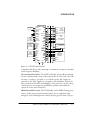
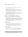
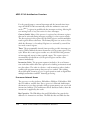
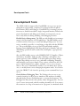
1 INTRODUCTION
Figure 1-0.
Table 1-0.
Listing 1-0.
Purpose
The ADSP-21160 SHARC DSP Hardware Reference provides architectural information on the ADSP-21160 Super Harvard Architecture
(SHARC) Digital Signal Processor (DSP). The architectural descriptions
cover functional blocks, busses, and ports, including all features and processes they support. For programming information, see the ADSP-21160
SHARC DSP Instruction Set Reference.
Audience
DSP system designers and programmers who are familiar with signal processing concepts are the primary audience for this manual. This manual
assumes that the audience has a working knowledge of microcomputer
technology and DSP-related mathematics.
DSP system designers and programmers who are unfamiliar with signal
processing can use this manual, but should supplement this manual with
other texts, describing DSP techniques.
All readers, particularly system designers, should refer to the DSP’s data
sheet for timing, electrical, and package specifications. For additional suggested reading, see “For More Information About Analog Products” on
page 1-22.
ADSP-21160 SHARC DSP Hardware Reference
1-1
Overview—Why Floating-Point DSP?
Overview—Why Floating-Point DSP?
A digital signal processor’s data format determines its ability to handle signals of differing precision, dynamic range, and signal-to-noise ratios.
Because floating-point DSP math reduces the need for scaling and probability of overflow, using a floating-point DSP can ease algorithm and
software development. The extent to which this is true depends on the
floating-point processor’s architecture. Consistency with IEEE workstation simulations and the elimination of scaling are two clear ease-of-use
advantages. High-level language programmability, large address spaces,
and wide dynamic range allow system development time to be spent on
algorithms and signal processing concerns, rather than assembly language
coding, code paging, and error handling. The ADSP-21160 is a highly
integrated, 32-bit floating-point DSP that provides many of these design
advantages.
ADSP-21160 Design Advantages
The ADSP-21160 is a high-performance 32-bit DSP for medical imaging,
communications, military, audio, test equipment, 3D graphics, speech
recognition, motor control, imaging, and other applications. This DSP
builds on the ADSP-21000 Family DSP core to form a complete system-on-a-chip, adding a dual-ported on-chip SRAM, integrated I/O
peripherals, and an additional processing element for Single-Instruction-Multiple-Data (SIMD) support.
SHARC is an acronym for Super Harvard Architecture. This DSP architecture balances a high performance processor core with high performance
buses (PM, DM, IO). In the core, every instruction can execute in a single
cycle. The buses and instruction cache provide rapid, unimpeded data
flow to the core to maintain the execution rate.
1-2
ADSP-21160 SHARC DSP Hardware Reference
INTRODUCTION
Figure 1-1 shows a detailed block diagram of the processor, illustrating the
following architectural features:
• Two Processing Elements (PEx and PEy), each containing a 32-Bit
IEEE floating-point computation units—multiplier, ALU, Shifter,
and data register file
• Program sequencer with related instruction cache, interval timer,
and Data Address Generators (DAG1 and DAG2)
• Dual-ported SRAM
• External port for interfacing to off-chip memory, peripherals, hosts,
and multiprocessor systems
• Input/Output (IO) processor with integrated DMA controller,
serial ports, and link ports for point-to-point multiprocessor communications
• JTAG Test Access Port for emulation
Figure 1-1 also shows the three on-chip buses of the ADSP-21160: the
Program Memory (PM) bus, Data Memory (DM) bus, and Input/Output
(IO) bus. The PM bus provides access to either instructions or data. During a single cycle, these buses let the processor access two data operands
(one from PM and one from DM), access an instruction (from the cache),
and perform a DMA transfer.
The buses connect to the ADSP-21160’s external port, which provides the
processor’s interface to external memory, memory-mapped I/O, a host
processor, and additional multiprocessing ADSP-21160s. The external
port performs bus arbitration and supplies control signals to shared, global
memory and I/O devices.
Figure 1-2 illustrates a typical single-processor system. The ADSP-21160
includes extensive support for multiprocessor systems as well. For more
information, see “Multiprocessor (DSPs) Interface” on page 7-91.
ADSP-21160 SHARC DSP Hardware Reference
1-3
ADSP-21160 Design Advantages
IN S T R U C T IO N
CACHE
TW O IN D E P E N D E N T
DU A L -P O R T ED B L O C K S
32 x 4 8-B IT
PRO CE SSO R P ORT
ADDR
DATA
ADDR
DAG1
DAG2
8x 4x32
8x 4x3 2
I/O PO RT
DATA
DA TA
ADDR
DATA
JTAG
BLO CK 1
TIME R
BLO CK 0
D U A L -P O R T ED S RA M
CORE PROCESSOR
6
TE ST &
E M U LA T IO N
ADDR
PR OG RAM
SE Q UENCE R
PM ADDRE S S BUS
32
DM ADDRE SS BUS
32
IO D
64
IO A
32
EXTERNAL
PORT
ADDR BU S
MU X
32
M ULTIP ROCESS OR
INTE RFACE
BUS
CO N N E C T
(PX)
PM DAT A BUS
48/64
DM DATA BUS
32 / 4 0 /6 4
64
DAT A BUS
MUX
HO ST PO RT
MULT
DATA
RE GIS TE R
FIL E
(P E x )
16 x 4 0 -BI T
BARRE L
S H IF T E R
BA R R E L
S H IF T E R
DATA
RE G IS TE R
FIL E
(P E y )
16 x 4 0 -BI T
MULT
IO P
RE GIS TE RS
(M E M O R Y
ALU
ALU
MAPP ED)
CO NTRO L,
ST ATUS, &
DATA BUF FERS
DM A
CO N T RO L L E R
4
6
SE RIAL PO RTS
(2 )
LINK PO RTS
(6 )
6
60
I/O P R O C E S S O R
Figure 1-1. ADSP-21160 SHARC Block Diagram
Further, the ADSP-21160 addresses the five central requirements for
DSPs:
• Fast, flexible arithmetic computation units
• Unconstrained data flow to and from the computation units
• Extended precision and dynamic range in the computation units
• Dual address generators with circular buffering support
• Efficient program sequencing
Fast, Flexible Arithmetic. The ADSP-21000 Family processors execute all
instructions in a single cycle. They provide both fast cycle times and a
complete set of arithmetic operations. The DSP is IEEE floating-point
1-4
ADSP-21160 SHARC DSP Hardware Reference
INTRODUCTION
A D S P-2116X
CL O C K
BMS
CL K IN
4
CL K _C F G 3-0
CS
AD DR
CIF
E BO O T
F LA G 3-0
T IM EXP
L INK
DE V IC E S
(6 M AX )
(O P T IO N AL )
S
SE
ERIA
RIALL
DE V IC E
DE V IC E
(O
(OPPTTIO
IONNAL
AL))
S
SE
E RIA
RIA L
L
DE
DE V
V IC
IC E
E
(OPPTTIO
IONNAL
AL))
(O
L X CL K
L X AC K
L X DA T 7-0
T CL K0
RC L K0
T FS 0
RS F 0
DT 0
DR 0
T CL K1
RC L K1
T FS 1
RS F 1
DT 1
DR 1
RP B A
AD D R31 -0
AD DR
DA T A 63-0
DA T A
RDX
WRX
WE
AC K
AC K
MS3-0
P AG E
SBTS
M E M O RY
AN D
P E RIP H ER AL S
(O P T IO N AL )
CS
DM A DE V ICE
(O P T IO N AL )
DA T A
CL K O U T
DMAR1-2
DMAG1-2
CS
HBR
HBG
RE D Y
HO S T
P RO CE S S O R
IN TE R FA CE
(O P T IO N AL )
BR1-6
AD DR
PA
DA T A
ID 2-0
RESET
OE
DA T A
IRQ2-0
A DD RE S S
4
DA T A
BR S T
C O NT RO L
L BO O T
3
BO O T
E P RO M
(O P T IO N AL )
JTA G
6
Figure 1-2. ADSP-21160 System
compatible and allows either interrupt on arithmetic exception or latched
status exception handling.
Unconstrained Data Flow. The ADSP-21160 has a Super Harvard Architecture combined with a 10-port data register file. In every cycle, the DSP
can write or read two operands to or from the register file, supply two
operands to the ALU, supply two operands to the multiplier, and receive
three results from the ALU and multiplier. The processor’s 48-bit orthogonal instruction word supports parallel data transfers and arithmetic
operations in the same instruction.
40-Bit Extended Precision. The DSP handles 32-bit IEEE floating-point
format, 32-bit integer and fractional formats (twos-complement and
unsigned), and extended-precision 40-bit floating-point format. The pro-
ADSP-21160 SHARC DSP Hardware Reference
1-5
ADSP-21160 Architecture Overview
cessors carry extended precision throughout their computation units,
limiting intermediate data truncation errors.
Dual Address Generators. The DSP has two data address generators
(DAGs) that provide immediate or indirect (pre- and post-modify)
addressing. Modulus, bit-reverse, and broadcast operations are supported
with no constraints on data buffer placement.
Efficient Program Sequencing. In addition to zero-overhead loops, the
DSP supports single-cycle setup and exit for loops. Loops are both
nestable (six levels in hardware) and interruptable. The processors support
both delayed and non-delayed branches.
ADSP-21160 Architecture Overview
The ADSP-21160 forms a complete system-on-a-chip, integrating a large,
high-speed SRAM and I/O peripherals supported by a dedicated I/O bus.
The following sections summarize the features of each functional block in
the ADSP-21160 SHARC architecture, which appears in Figure 1-1.
With each summary, a cross reference points to the sections where the features are described in greater detail.
Processor Core
The processor core of the ADSP-21160 consists of two processing elements (each with three computation units and data register file), a
program sequencer, two data address generators, a timer, and an instruction cache. All digital signal processing occurs in the processor core.
Processing Elements
The processor core contains two Processing Elements (PEx and PEy).
Each element contains a data register file and three independent computation units: an ALU, a multiplier with a fixed-point accumulator, and a
1-6
ADSP-21160 SHARC DSP Hardware Reference
INTRODUCTION
shifter. For meeting a wide variety of processing needs, the computation
units process data in three formats: 32-bit fixed-point, 32-bit floating-point and 40-bit floating-point. The floating-point operations are
single-precision IEEE-compatible. The 32-bit floating-point format is the
standard IEEE format, whereas the 40-bit extended-precision format has
eight additional Least Significant Bits (LSBs) of mantissa for greater
accuracy.
The ALU performs a set of arithmetic and logic operations on both
fixed-point and floating-point formats. The multiplier performs floating-point or fixed-point multiplication and fixed-point multiply/add or
multiply/subtract operations. The shifter performs logical and arithmetic
shifts, bit manipulation, field deposit and extraction, and exponent derivation operations on 32-bit operands. These computation units perform
single-cycle operations; there is no computation pipeline. All units are
connected in parallel, rather than serially. The output of any unit may
serve as the input of any unit on the next cycle. In a multifunction computation, the ALU and multiplier perform independent, simultaneous
operations.
Each processing element has a general-purpose data register file that transfers data between the computation units and the data buses and stores
intermediate results. A register file has two sets (primary and alternate) of
sixteen registers each, for fast context switching. All of the registers are 40
bits wide. The register file, combined with the core processor’s Harvard
architecture, allows unconstrained data flow between computation units
and internal memory.
Primary Processing Element (PEx). PEx processes all computational
instructions whether the DSP is in Single-Instruction, Single-Data (SISD)
or Single-Instruction, Multiple-Data (SIMD) mode. This element corresponds to the computational units and register file in previous
ADSP-21000 family DSPs.
Secondary Processing Element (PEy). PEy processes each computational
instruction in lock-step with PEx, but only processes these instructions
ADSP-21160 SHARC DSP Hardware Reference
1-7
ADSP-21160 Architecture Overview
when the DSP is in SIMD mode. Because many operations are influenced
by this mode, more information on SIMD is available in multiple
locations:
• For information on PEy operations, see “Processing Elements” on
page 2-1
• For information on data addressing in SIMD mode, see “Addressing
in SISD & SIMD Modes” on page 4-17
• For information on data accesses in SIMD mode, see “SISD, SIMD,
and Broadcast Load Modes” on page 5-45
• For information on multiprocessing in SIMD mode, see “Multiprocessor (DSPs) Interface” on page 7-91
• For information on SIMD programming, see the ADSP-21160
SHARC DSP Instruction Set Reference.
Program Sequence Control
Internal controls for ADSP-21160 program execution come from four
functional blocks: program sequencer, data address generators, timer, and
instruction cache. Two dedicated address generators and a program
sequencer supply addresses for memory accesses. Together the sequencer
and data address generators allow computational operations to execute
with maximum efficiency since the computation units can be devoted
exclusively to processing data. With its instruction cache, the
ADSP-21160 can simultaneously fetch an instruction from the cache and
access two data operands from memory. The data address generators
implement circular data buffers in hardware.
Program Sequencer. The program sequencer supplies instruction
addresses to program memory. It controls loop iterations and evaluates
conditional instructions. With an internal loop counter and loop stack,
the ADSP-21160 executes looped code with zero overhead. No explicit
1-8
ADSP-21160 SHARC DSP Hardware Reference
INTRODUCTION
jump instructions are required to loop or to decrement and test the
counter.
The ADSP-21160 achieves its fast execution rate by means of pipelined
fetch, decode and execute cycles. If external memories are used, they are
allowed more time to complete an access than if there were no decode
cycle.
Data Address Generators. The data address generators (DAGs) provide
memory addresses when data is transferred between memory and registers.
Dual data address generators enable the processor to output simultaneous
addresses for two operand reads or writes. DAG1 supplies 32-bit addresses
to data memory. DAG2 supplies 32-bit addresses to program memory for
program memory data accesses.
Each DAG keeps track of up to eight address pointers, eight modifiers and
eight length values. A pointer used for indirect addressing can be modified
by a value in a specified register, either before (pre-modify) or after
(post-modify) the access. A length value may be associated with each
pointer to perform automatic modulo addressing for circular data buffers;
the circular buffers can be located at arbitrary boundaries in memory.
Each DAG register has an alternate register that can be activated for fast
context switching.
Circular buffers allow efficient implementation of delay lines and other
data structures required in digital signal processing, and are commonly
used in digital filters and Fourier transforms. The DAGs automatically
handle address pointer wraparound, reducing overhead, increasing performance, and simplifying implementation.
Interrupts. The ADSP-21160 has four external hardware interrupts: three
general-purpose interrupts, IRQ2-0, and a special interrupt for reset. The
processor also has internally generated interrupts for the timer, DMA controller operations, circular buffer overflow, stack overflows, arithmetic
exceptions, multiprocessor vector interrupts, and user-defined software
interrupts.
ADSP-21160 SHARC DSP Hardware Reference
1-9
ADSP-21160 Architecture Overview
For the general-purpose external interrupts and the internal timer interrupt, the ADSP-21160 automatically stacks the arithmetic status and
mode (MODE1) registers in parallel with the interrupt servicing, allowing fifteen nesting levels of very fast service for these interrupts.
Context Switch. Many of the processor’s registers have alternate registers
that can be activated during interrupt servicing for a fast context switch.
The data registers in the register file, the DAG registers, and the multiplier
result register all have alternates. The Primary Registers are active at reset,
while the Alternate (or Secondary) Registers are activated by control bits
in a mode control register.
Timer. The programmable interval timer provides periodic interrupt generation. When enabled, the timer decrements a 32-bit count register every
cycle. When this count register reaches zero, the ADSP-21160 generates
an interrupt and asserts its timer expired output. The count register is
automatically reloaded from a 32-bit period register and the count
resumes immediately.
Instruction Cache. The program sequencer includes a 32-word instruction cache that enables three-bus operation for fetching an instruction and
two data values. The cache is selective—only instructions whose fetches
conflict with program memory data accesses are cached. This caching
allows full-speed execution of core, looped operations such as digital filter
multiply-accumulates and FFT butterfly processing.
Processor Internal Buses
The processor core has six buses: PM address, PM data, DM address, DM
data, IO address, and IO data. Due to processor’s Harvard Architecture,
data memory stores data operands, while program memory can store both
instructions and data. This architecture allows dual data fetches, when the
instruction is supplied by the cache.
Bus Capacities. The PM address bus and DM address bus transfer the
addresses for instructions and data. The PM data bus and DM data bus
1-10
ADSP-21160 SHARC DSP Hardware Reference
INTRODUCTION
transfer the data or instructions from each type of memory. The PM
address bus is 32 bits wide allowing access of up to 4 Gwords of mixed
instructions and data. The PM data bus is 64 bits wide to accommodate
the 48-bit instructions and 64-bit data.
The DM address bus is 32 bits wide allowing direct access of up to 4G
words of data. The DM data bus is 64 bits wide. The DM data bus provides a path for the contents of any register in the processor to be
transferred to any other register or to any data memory location in a single
cycle. The data memory address comes from one of two sources: an absolute value specified in the instruction code (direct addressing) or the
output of a data address generator (indirect addressing).
The IO address and IO data buses let the IO processor access internal
memory for DMA without delaying the processor core. The IO address
bus is 32 bits wide, and the IO data bus is 64 bits wide.
Data Transfers. Nearly every register in the processor core is classified as a
Universal Register (UREG). Instructions allow transferring data between
any two universal registers or between a universal register and memory.
This support includes transfers between control registers, status registers,
and data registers in the register file. The PM bus connect ( PX) registers
permit data to be passed between the 64-bit PM data bus and the 64-bit
DM data bus or between the 40-bit register file and the PM data bus.
These registers contain hardware to handle the data width difference. For
more information, see “Processing Element Registers” on page A-19.
Processor Peripherals
The term processor peripherals refers to everything outside the processor
core. The ADSP-21160’s peripherals include internal memory, external
port, I/O processor, JTAG port, and any external devices that connect to
the DSP.
ADSP-21160 SHARC DSP Hardware Reference
1-11
ADSP-21160 Architecture Overview
Dual-Ported Internal Memory (SRAM)
The ADSP-21160 contains 4 megabits of on-chip SRAM, organized as
two blocks of 2 Mbits each, which can be configured for different combinations of code and data storage. Each memory block is dual-ported for
single-cycle, independent accesses by the core processor and I/O processor
or DMA controller. The dual-ported memory and separate on-chip buses
allow two data transfers from the core and one from I/O, all in a single
cycle.
All of the memory can be accessed as 16-, 32-, 48-, or 64-bit words. On
the ADSP-21160, the memory can be configured as a maximum of 128K
words of 32-bit data, 256K words of 16-bit data, 80K words of 48-bit
instructions (and 40-bit data), or combinations of different word sizes up
to 4 megabits.
The DSP supports a 16-bit floating-point storage format, which effectively doubles the amount of data that may be stored on chip. Conversion
between the 32-bit floating-point and 16-bit floating-point formats completes in a single instruction.
While each memory block can store combinations of code and data,
accesses are most efficient when one block stores data, using the DM bus
for transfers, and the other block stores instructions and data, using the
PM bus for transfers. Using the DM bus and PM bus in this way, with one
dedicated to each memory block, assures single-cycle execution with two
data transfers. In this case, the instruction must be available in the cache.
The DSP also maintains single-cycle execution when one of the data operands is transferred to or from off-chip, using the DSP’s external port.
External Port
The ADSP-21160’s external port provides the processor’s interface to
off-chip memory and peripherals. The 4-gigaword off-chip address space
is included in the ADSP-21160’s unified address space. The separate
on-chip buses—for PM address, PM data, DM address, DM data, IO
1-12
ADSP-21160 SHARC DSP Hardware Reference
INTRODUCTION
address, and IO data—multiplex at the external port to create an external
system bus with a single 32-bit address bus and a single 64-bit data bus.
External SRAM can be 16, 32, 48, or 64 bits wide; the ADSP-21160’s
on-chip DMA controller automatically packs external data into the appropriate word width during transfers.
On-chip decoding of high-order address lines generates memory bank
select signals for addressing external memory devices. Separate control
lines support simplified addressing of page-mode DRAM. The
ADSP-21160 provides programmable memory waitstates and external
memory acknowledge controls for interfacing to DRAM and peripherals
with variable access, hold, and disable time requirements.
Host Processor Interface. The ADSP-21160’s host interface allows easy
connection to standard microprocessor buses, both 16-bit and 32-bit,
with little additional hardware required. The interface supports asynchronous and synchronous transfers at speeds up to the half the internal clock
rate of the ADSP-21160. The host interface operates through the
ADSP-21160’s external port and maps into the unified address space.
Four channels of DMA are available for the host interface; code and data
transfers occur with low software overhead. The host can directly read and
write the internal memory of the ADSP-21160 and can access the DMA
channel setup and mailbox registers. Vector interrupt support provides for
efficient execution of host commands.
Multiprocessor System Interface. The ADSP-21160 offers powerful features tailored to multiprocessing DSP systems. The unified address space
allows direct interprocessor accesses of each ADSP-21160’s internal memory. Distributed bus arbitration logic on the DSP allows simple, glueless
connection of systems containing up to six ADSP-21160s and a host processor. Master processor changeover incurs only one cycle of overhead.
Bus arbitration handles either fixed or rotating priority. Processor bus lock
allows indivisible read-modify-write sequences for semaphores. A vector
interrupt capability is provided for interprocessor commands. Broadcast
ADSP-21160 SHARC DSP Hardware Reference
1-13
ADSP-21160 Architecture Overview
writes allow simultaneous transmission of data to all ADSP-21160s and
can be used to implement reflective semaphores.
I/O Processor
The ADSP-21160’s Input/Output Processor (IOP) includes two serial
ports, six link ports, and a DMA controller. One of the I/O processes that
the IO processor automates is booting. The DSP can boot from the external port (with data from an 8-bit EPROM or a host processor) or a link
port. Alternatively, a no-boot mode lets the DSP start by executing
instructions from external memory without booting.
Serial Ports. The ADSP-21160 features two synchronous serial ports that
provide an inexpensive interface to a wide variety of digital and mixed-signal peripheral devices. The serial ports can operate at up to half the
processor core clock rate. Independent transmit and receive functions provide greater flexibility for serial communications. Serial port data can
automatically transfer to and from on-chip memory using DMA. Each of
the serial ports offers a TDM multichannel mode and supports µ-law or
A-law companding.
The serial ports can operate with little-endian or big-endian transmission
formats, with word lengths selectable from 3 to 32 bits. They offer selectable synchronization and transmit modes. Serial port clocks and frame
syncs can be internally or externally generated.
Link Ports. The ADSP-21160 features six 10-bit link ports that provide
additional I/O capabilities. Link port I/O is especially useful for
point-to-point interprocessor communication in multiprocessing systems.
The link ports can operate independently and simultaneously. The data
packs into 32-bit or 48-bit words, which the processor core can directly
read or the IO processor can DMA-transfer to on-chip memory.
Clock/acknowledge handshaking controls link port transfers. Transfers are
programmable as either transmit or receive.
1-14
ADSP-21160 SHARC DSP Hardware Reference
INTRODUCTION
DMA Controller. The ADSP-21160’s on-chip DMA controller allows
zero-overhead data transfers without processor intervention. The DMA
controller operates independently and invisibly to the processor core,
allowing DMA operations to occur while the core is simultaneously executing its program. Both code and data can be downloaded to the
ADSP-21160 using DMA transfers.
DMA transfers can occur between the ADSP-21160’s internal memory
and external memory, external peripherals, or a host processor. DMA
transfers can also occur between the ADSP-21160’s internal memory and
its serial ports or link ports. DMA transfers between external memory and
external peripheral devices are another option. External bus packing to
16-, 32-, 48-, or 64-bit words is automatically performed during DMA
transfers.
Fourteen channels of DMA are available on the ADSP-21160—six over
the link ports, four over the serial ports, and four over the processor’s
external port. The external port DMA channels serve for host processor,
other ADSP-21160s, memory, or I/O transfers.
JTAG Port
The JTAG port on the ADSP-21160 supports the IEEE standard 1149.1
Joint Test Action Group (JTAG) standard for system test. This standard
defines a method for serially scanning the I/O status of each component in
a system. Emulators use the JTAG port to monitor and control the DSP
during emulation. Emulators using this port provide full-speed emulation
with access to inspect and modify memory, registers, and processor stacks.
JTAG-based emulation is non-intrusive and does not effect target system
loading or timing.
ADSP-21160 SHARC DSP Hardware Reference
1-15
Development Tools
Development Tools
The ADSP-21160 is supported by VisualDSP®, an easy-to-use project
management environment, comprised of an Integrated Development
Environment (IDE) and Debugger. VisualDSP lets you manage projects
from start to finish from within a single, integrated interface. Because the
project development and debug environments are integrated, you can
move easily between editing, building, and debugging activities.
Flexible Project Management. The IDE provides flexible project management for the development of DSP applications. The IDE includes access
to all the activities necessary to create and debug DSP projects. You can
create or modify source files or view listing or map files with the IDE Editor. This powerful Editor is part of the IDE and includes multiple
language syntax highlighting, OLE drag and drop, bookmarks, and standard editing operations such as undo/redo, find/replace, copy/paste/cut,
and go to.
Also, the IDE includes access to the SHARC® DSP C Compiler, C Runtime Library, Assembler, Linker, Loader, Simulator, and Splitter. You
specify options for these SHARC Tools through Property Page dialogs.
Property Page dialogs are easy to use, and make configuring, changing,
and managing your projects simple. These options control how the tools
process inputs and generate outputs, and have a one-to-one correspondence to the tools’ command line switches. You can define these options
once, or modify them to meet changing development needs. You can also
access the SHARC Tools from the operating system command line if you
choose.
Greatly Reduced Debugging Time. The Debugger has an easy-to-use,
common interface for all processor simulators and emulators available
through Analog Devices and third parties or custom developments. The
Debugger has many features that greatly reduce debugging time. You can
view C source interspersed with the resulting Assembly code. You can profile execution of a range of instructions in a program; set simulated watch
1-16
ADSP-21160 SHARC DSP Hardware Reference
INTRODUCTION
points on hardware and software registers, program and data memory; and
trace instruction execution and memory accesses. These features enable
you to correct coding errors, identify bottlenecks, and examine DSP performance. You can use the custom register option to select any
combination of registers to view in a single window. The Debugger can
also generate inputs, outputs, and interrupts so you can simulate real
world application conditions.
SHARC Software Development Tools. SHARC Software Development
Tools, which support the SHARC Family, allow you to develop applications that take full advantage of the SHARC architecture, including
multiprocessing, shared memory, and memory overlays. SHARC Software
Development Tools include C Compiler, C Runtime Library, DSP and
Math Libraries, Assembler, Linker, Loader, Simulator, and Splitter.
C Compiler & Assembler. The C Compiler generates efficient code that is
optimized for both code density and execution time. The C Compiler
allows you to include Assembly language statements inline. Because of
this, you can program in C and still use Assembly for time-critical loops.
You can also use pretested Math, DSP, and C Runtime Library routines to
help shorten your time to market. The SHARC Family Assembly language
is based on an algebraic syntax that is easy to learn, program, and debug.
The add instruction, for example, is written in the same manner as the
actual equation.
Linker & Loader. The Linker provides flexible system definition through
Linker Description Files (.LDF). In a single LDF, you can define different
types of executables for a single or multiprocessor system. The Linker
resolves symbols over multiple executables, maximizes memory use, and
easily shares common code among multiple processors. The Loader supports creation of host, link port, and PROM boot images. Along with the
Linker, the Loader allows multiprocessor system configuration with
smaller code and faster boot time. The Simulator is a cycle-accurate,
instruction-level simulator — allowing you to simulate your application in
real time.
ADSP-21160 SHARC DSP Hardware Reference
1-17
Differences From Previous SHARC DSPs
3rd-Party Extensible. The VisualDSP environment enables third-party
companies to add value using Analog Devices' published set of Application Programming Interfaces (API). Third party products—runtime
operating systems, emulators, high-level language compilers, multiprocessor hardware —can interface seamlessly with VisualDSP thereby
simplifying the tools integration task. VisualDSP follows the COM API
format. Two API tools, Target Wizard and API Tester, are also available
for use with the API set. These tools help speed the time-to-market for
vendor products. Target Wizard builds the programming shell based on
API features the vendor requires. The API tester exercises the individual
features independently of VisualDSP. Third parties can use a subset of
these APIs that meets their application needs. The interfaces are fully supported and backward compatible.
Further details and ordering information are available in the VisualDSP
Development Tools data sheet. This data sheet can be requested from any
Analog Devices sales office or distributor.
Differences From Previous SHARC DSPs
This section identifies differences between the ADSP-21160 DSP and previous SHARC DSPs: ADSP-21060, ADSP-21061, and ADSP-21062. The
ADSP-21160 preserves much of the ADSP-2106x architecture, while
extending performance and functionality. For background information on
SHARC and the ADSP-2106x Family DSPs, see the ADSP-2106x
SHARC User’s Manual.
Processor Core Enhancements
Computational bandwidth on the ADSP-21160 is significantly greater
that on the ADSP-2106x DSPs. The increase comes from raising the operational frequency and adding another processing element: ALU, Shifter,
Multiplier, and register file. The new processing element lets the DSP process multiple data streams in parallel (SIMD mode).
1-18
ADSP-21160 SHARC DSP Hardware Reference
INTRODUCTION
The program sequencer on the ADSP-21160 differs from the
ADSP-2106x family, having several enhancements: new interrupt vector
table definitions, SIMD mode stack and conditional execution model, and
instruction decodes associated with new instructions. Changes to interrupts include new interrupt vectors for detecting illegal memory accesses
and supporting new unshared DMA channels. Link port interrupt control
has moved to a new register to support the additional DMA channels.
Also, new mode stack and mode mask support has been added to improve
context switch time.
Data address generators on the ADSP-21160 differ from the ADSP-2106x
in that DAG2 (for the PM bus) has the same addressing capability as
DAG1 (for the DM bus). The DAG registers are read/writable in pairs,
moving 64-bits/cycle. Additionally, the DAGs support the new memory
map and Long Word transfer capability. Circular buffering on the
ADSP-21160 can be quickly disabled on interrupts and restored on the
return. Data “broadcast”, from one memory location to both data register
files, is determined by appropriate index register usage.
previous SHARCs, the ADSP-21160 has a global circular
! Unlike
buffering enable (
) bit. Because at reset this bit defaults to
CBUFEN
disabled, programs that use circular buffering and are being ported
from previous SHARCs need to add a line of code to enable circular
buffering. For more information, see “Addressing Circular Buffers”
on page 4-12.
Processor Internal Bus Enhancements
The PM, DM, and IO data buses on the ADSP-21160 are much wider
than on the ADSP-2106x DSPs, increasing to 64 bits. Additional multiplexing and control logic on the ADSP-21160 enable 16-, 32-, or 64-bit
wide moves between both register files and memory. The ADSP-21160
also has the capability of broadcasting a single memory location to each of
the register files in parallel. Also, the ADSP-21160 permits register con-
ADSP-21160 SHARC DSP Hardware Reference
1-19
Differences From Previous SHARC DSPs
tents to be exchanged between the two processing elements’ register files
in a single cycle.
Memory Organization Enhancements
The ADSP-21160 memory map differs from the ADSP-2106x DSPs. The
system memory map on the ADSP-21160 supports double-word transfers
each cycle, reflects extended internal memory capacity for derivative
designs, and works with updated control register for SIMD support.
External Port Enhancements
The ADSP-21160’s external port differs from the ADSP-2106x DSPs,
greatly extending the external interface. The data bus on the ADSP-21160
is 64 bits wide. The ADSP-21160 has a new synchronous interface that
improves local bus switching frequency. Also, burst support on the
ADSP-21160 improves bus usage.
previous SHARCs, the ADSP-21160 sets the buffer hang
! Unlike
disable ( ) bit at reset. Because this bit prevents the processor core
BHD
from detecting a buffer-related stall condition, programs that use
external port, link port, or serial port I/O and are being ported from
previous SHARCs need to add a line of code to disable BHD. For
more information, see the BHD discussion on page 6-18.
Host Interface Enhancements
The ADSP-21160’s host interface differs from the ADSP-2106x DSPs in
that this interface can take advantage of the 64-bit data bus width.
Though the ADSP-21160 supports the ADSP-2106x’s asynchronous host
interface protocols, the ADSP-21160 also provides new synchronous
interface protocols for maximum throughput.
The host/local bus deadlock resolution function on the ADSP-21160 is
extended to the DMA controller. The function allows the host (or bridge)
1-20
ADSP-21160 SHARC DSP Hardware Reference
INTRODUCTION
logic to force the local bus to back off and allow the host to complete it’s
operation first.
Multiprocessor Interface Enhancements
The ADSP-21160’s multiprocessor system interface supports greater
throughput than the ADSP-2106x DSPs. The throughput between
ADSP-21160s in a multiprocessing application increases due to shared
data bus width increase to 64-bits, new shared bus transfer protocols,
shared bus cycle time improvements due to synchronous interface, and
improvements in Link Port throughput. The external port supports glueless multiprocessing, with distributed arbitration for up to six
ADSP-21160s.
IO Architecture Enhancements
The IO processor on the ADSP-21160 provides much greater throughput
than the ADSP-2106x DSPs. The Link Ports and DMA controller differ
on the ADSP-21160.
DMA Controller Enhancements
The ADSP-21160’s DMA controller supports 14 channels (versus 10 on
the ADSP-2106x DSPs), with no channel sharing. New packing modes
support the new 64-bit external/internal busing. To resolve potential
deadlock scenarios, the ADSP-21106’s DMA controller relinquishes the
local bus in a similar fashion to the processor core when host logic asserts
both HBR and SBTS.
Link Port Enhancements
The ADSP-21160’s Link ports provide greater throughput than the
ADSP-2106x DSPs. The link port data bus width on the ADSP-21160 is
8 bits wide (versus 4 bits on the ADSP-2106x DSPs). Link port clock control on the ADSP-21160 supports a wider frequency range.
ADSP-21160 SHARC DSP Hardware Reference
1-21
For More Information About Analog Products
Instruction Set Enhancements
ADSP-21160 provides source code compatibility with the previous
SHARC family members, to the application assembly source code level.
All instructions, control registers, and system resources available in the
ADSP-2106x core programming model are available in ADSP-21160.
New instructions, control registers, or other facilities, required to support
the new feature set of ADSP-21160 core are:
• Supersets of the ADSP-2106x programming model
• Reserved facilities in the ADSP-2106x programming model
• Symbol name changes from the ADSP-2106x programming model
These name changes can be managed through re-assembly using the
ADSP-21160 development tools to apply the ADSP-21160 symbol definitions header file and linker description file. While these changes have no
direct impact on existing core applications, system and I/O processor initialization code and control code do require modifications.
This approach simplifies porting of source code written for the
ADSP-2106x family to ADSP-21160. Code changes will be required to
take full advantage of the new ADSP-21160 features. For more
information, see the ADSP-21160 SHARC DSP Instruction Set Reference.
For More Information About Analog
Products
Analog Devices is online on the internet at http://www.analog.com. Our
Web pages provide information on the company and products, including
access to technical information and documentation, product overviews,
and product announcements.
1-22
ADSP-21160 SHARC DSP Hardware Reference
INTRODUCTION
You may also obtain additional information about Analog Devices and its
products in any of the following ways:
• Visit our World Wide Web site at www.analog.com
• FAX questions or requests for information to 1(781)461-3010.
• Access the Computer Products Division File Transfer Protocol
(FTP) site at ftp ftp.analog.com or ftp 137.71.23.21 or
ftp://ftp.analog.com.
For Technical or Customer Support
You can reach our Customer Support group in the following ways:
• E-mail questions to [email protected] or
[email protected] (European customer support)
• Telex questions to 924491, TWX:710/394-6577
• Cable questions to ANALOG NORWOODMASS
• Contact your local ADI sales office or an authorized ADI distributor
• Send questions by mail to:
Analog Devices, Inc.
DSP Division
One Technology Way
P.O. Box 9106
Norwood, MA 02062-9106
USA
What’s New in This Manual
This is the first edition of the ADSP-21160 SHARC DSP Hardware Reference. Summaries of changes between editions will start with the next
edition.
ADSP-21160 SHARC DSP Hardware Reference
1-23
Related Documents
Related Documents
For more information about Analog Devices DSPs and development
products, see the following documents:
• ADSP-21160 SHARC DSP Microcomputer Data Sheet
• ADSP-21160 SHARC DSP Instruction Set Reference
• Getting Started Guide for VisualDSP & ADSP-21xxx Family DSPs
• VisualDSP User's Guide for ADSP-21xxx Family DSPs
• C Compiler & Library Manual for ADSP-21xxx Family DSPs
• Assembler Manual for ADSP-21xxx Family DSPs
• Linker & Utilities Manual for ADSP-21xxx Family DSPs
All the manuals are included in the software distribution CD-ROM. To
access these manuals, use the Help Topics command in the VisualDSP
environment’s Help menu and select the Online Manuals book. From this
Help topic, you can open any of the manuals, which are in Adobe Acrobat
PDF format.
1-24
ADSP-21160 SHARC DSP Hardware Reference
INTRODUCTION
Conventions
The following are conventions that apply to all chapters. Note that additional conventions, which apply only to specific chapters, appear
throughout this document.
Table 1-1. Notation Conventions
Example
Description
PC, R1, PX
Register names appear in UPPERCASE and keyword font
TIMEXP, RESET
Pin names appear in UPPERCASE and keyword font; active
low signals appear with an OVERBAR.
If, Do/Until
Assembler instructions (mnemonics) appear in initial capitals
!
A note, providing information of special interest or identifying a
related DSP topic.
"
A caution, providing information on critical design or programming issues that influence operation of the DSP.
Click Here
In the online version of this document, a cross reference acts as a
hypertext link to the item being referenced. Click on blue references (Table, Figure, or section names) to jump to the location.
ADSP-21160 SHARC DSP Hardware Reference
1-25
Conventions
1-26
ADSP-21160 SHARC DSP Hardware Reference