1
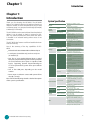
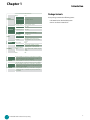
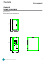
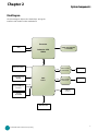
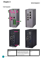
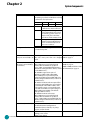
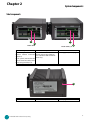
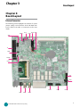
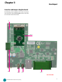
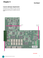
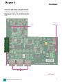
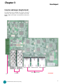
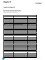
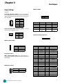
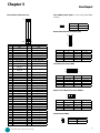
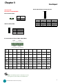
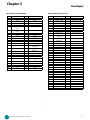
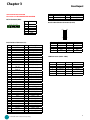
Industrial
Communications
Hardware Platforms for Industrial Computing
LEC-6020
V1.0
>>
User's Manual
Publication date: 2014-07-04
About
About
Overview
Acknowledgement
Icon Descriptions
The icons are used in the manual to serve as an indication
of interest topics or important messages. Below is a
description of these icons:
NOTE: This check mark indicates that
there is a note of interest and is something
that you should pay special attention to
while using the product.
WARNING: This exclamation point
indicates that there is a caution or
warning and it is something that could
damage your property or product.
Intel, Pentium and Celeron are registered trademarks of
Intel Corp.
Microsoft Windows and MS-DOS are registered trademarks
of Microsoft Corp.
All other product names or trademarks are properties of
their respective owners.
Compliances and Certification
CE Certification
This product has passed the CE test for environmental
specifications. Test conditions for passing included the
equipment being operated within an industrial enclosure.
In order to protect the product from being damaged by
ESD (Electrostatic Discharge) and EMI leakage, we strongly
recommend the use of CE-compliant industrial enclosure
products.
FCC Class A Certification
Online Resources
The listed websites are links to the on-line product
information and technical support.
Resource
Website
Lanner
http://www.lannerinc.com
Product Resources
h t t p : / / w w w. l a n n e r i n c. co m /
support/download-center
RMA
http://eRMA.lannerinc.com
This equipment has been tested and found to comply
with the limits for a Class A digital device, pursuant to Part
15 of the FCC Rules. These limits are designed to provide
reasonable protection against harmful interference when
the equipment is operated in a commercial environment.
This equipment generates, uses and can radiate radio
frequency energy and, if not installed and used in
accordance with the instruction manual, may cause
harmful interference to radio communications. Operation
of this equipment in a residential area is likely to cause
harmful interference in which case the user will be required
to correct the interference at his own expense.
Copyright and Trademarks
This document is copyrighted, © 2014. All rights are
reserved. The original manufacturer reserves the right to
make improvements to the products described in this
manual at any time without notice.
No part of this manual may be reproduced, copied,
translated or transmitted in any form or by any means
without the prior written permission of the original
manufacturer. Information provided in this manual is
intended to be accurate and reliable. However, the original
manufacturer assumes no responsibility for its use, nor for
any infringements upon the rights of third parties that
may result from such use.
Embedded and Industrial Computing
2
TTaTTable of Contentsbeable of Conte
Chapter 1: Introduction
4
System Specification . . . . . . . . . . . . . . . . . . . . . . . . . . . . . . . . . . . . . . . . . . . . 4
Package Contents . . . . . . . . . . . . . . . . . . . . . . . . . . . . . . . . . . . . . . . . . . . . . . 5
Chapter 2: System Components
6
System Drawing . . . . . . . . . . . . . . . . . . . . . . . . . . . . . . . . . . . . . . . . . . . . . . . 6
Block Diagram . . . . . . . . . . . . . . . . . . . . . . . . . . . . . . . . . . . . . . . . . . . . . . . . 7
Front Components . . . . . . . . . . . . . . . . . . . . . . . . . . . . . . . . . . . . . . . . . . . . . 8
Side Components . . . . . . . . . . . . . . . . . . . . . . . . . . . . . . . . . . . . . . . . . . . . . 10
Chapter 3: Board Layout
11
External Connectors . . . . . . . . . . . . . . . . . . . . . . . . . . . . . . . . . . . . . . . . . . . 11
Connectors and Jumpers (daughter board) . . . . . . . . . . . . . . . . . . . . . . . . . . . . . 12
Connectors and Jumpers (daughter board) . . . . . . . . . . . . . . . . . . . . . . . . . . . . . 13
Connectors and Jumpers (daughter board) . . . . . . . . . . . . . . . . . . . . . . . . . . . . . 14
Connectors and Jumpers (daughter board) . . . . . . . . . . . . . . . . . . . . . . . . . . . . . 15
Connectors and Jumpers List . . . . . . . . . . . . . . . . . . . . . . . . . . . . . . . . . . . . . 16
Jumper Settings . . . . . . . . . . . . . . . . . . . . . . . . . . . . . . . . . . . . . . . . . . . . . . 17
Chapter 4: Hardware Setup
23
Preparing the Hardware Installation . . . . . . . . . . . . . . . . . . . . . . . . . . . . . . . . . 23
Installing the System Memory . . . . . . . . . . . . . . . . . . . . . . . . . . . . . . . . . . . . . 23
Installing a CompactFlash Card . . . . . . . . . . . . . . . . . . . . . . . . . . . . . . . . . . . . 24
Connecting Power . . . . . . . . . . . . . . . . . . . . . . . . . . . . . . . . . . . . . . . . . . . . 24
Appendix A: Programming Watchdog Timer
25
3
Chapter 1
Chapter 1:
Introduction
Thank you for choosing the LEC-6020. The LEC-6020
series is an industrial cyber security appliance featuring a
different number of serial communication ports as well
as Ethernet ports in a compact frame design (65mm(W)
x146mm(H) x127mm(D)).
The LEC-6020 has an innovative industrial and mechanical
design. It can be placed on desk or mounted on dinrails. This reduces maintenance effort when the device
is installed in an industrial setting where access is not
convenient.
The LEC-6020 also features a solid and sealed aluminum
extrusion framing.
Here is the summary of the key capabilities of LEC6020:
•• Onboard Intel Atom N2600 with Intel NM10 chipset
Introduction
System Specification
Processor Options
Chipset
BIOS
Sockets
System
Technology
Memory
Max. Capacity
USB
Expansion Bus
OS Support
NAND Flash
Storage
HDD Support
Expansion
•• 4 serial ports (on model A only) and one serial port
(on model C, D)
•• Two, five or seven gigabit Ethernet RJ-45 or optical
fiber ports (all ports have magnetic isolation protection
of 1.5 KV). Moreover, these ports are capable of LAN
bypass, supporting dynamic disconnection/bypass
on a host system failure, power off or upon software
request.
LAN
Networking
•• Two or four USB ports depending on the model
Controller
number
•• Power input via Phoenix contact with power failure
Magnetic Isolation
Protection
relay (B, C, D only)
Please refer to the following chart for a detailed description
of the system's specifications.
Serial Interface
Serial Signals
Display
LEDs
Embedded and Industrial Computing
Serial Standard
ESD Protection
RS-232
RS-422
RS-485
Baudrate
Graphics Controller
Display Interface
Intel® Atom™ N2600 1.6 GHz
Intel NM10
AMI 8Mbit SPI Flash ROM
1 x 204-pin DDR3 SODIMM socket
Dual-Channel DDR3 1066/1333MHz,
unbuffered, Non-ECC
2 GB
LEC-6020A: USB 2.0 compliant hosts x
4, Type A connector
LEC-6020B/C/D: USB 2.0 compliant
hosts x 2, Type A connector
Mini-PCIe (LEC-6020A only)
LEC-6020A/B/D: Linux 2.6, Windows
XP Embedded, Window XP, Window 7
Embdded
LEC-6020C: Linux 2.6, Windows 7
Embedded
None
SATA connector for SSD/HDD expansion, HDD mounting kits (by request)
CompactFlash socket Type I/II x1
LEC-6020A: 3 x 10/100/1000 Mbps
ports, Autosensing, RJ45, with one pair
of LAN bypass.
LEC-6020B: 5 x 10/100/1000 Mbps
ports, Autosensing, RJ45, with two pairs
of LAN bypass
LEC-6020C: 5x10/100/1000Mbps
ports, Autosensing, RJ45, with one pair
bypass. 2x Gigabit SFP
LEC-6020D: 5x10/100/1000Mbps
ports, Autosensing, RJ45, with one pair
bypass.
LEC-6020A: Intel 82574L x 3,
LEC-6020B/D: Intel 82574L x 5,
LEC-6020C: Intel 82574L x 2, Intel
I210x5
1.5 KV built-in
LEC-6020A: 2 x 10 pin terminal block
for 4 x RS-232/422/485, 1 x internal
header (RS232 only)
LEC-6020B: 1 x internal header for
RS-232
LEC-6020C/D: 1 x DB9 for RS-232
15 KV for all signals
RTS, Rx, Tx, CTS, GND
TxD+, TxD-, RxD-, RxD+, GND
Data+, Data-, GND
Supports 50 bps to 115.2 kbps
Intel® GMA 3600
internal pin header
LEC-6020A: Power, Storage, Run (user
defined), 3 x User defined, 4 x Rx, 4
x Tx.
LEC-6020B/D: Power, Storage, Run
(user defined), 3 x User defined
LEC-6020C: Power, Storage, Run(User
defined), 3x User deined, 2x SFP.
4
Chapter 1
Housing
Weight
Introduction
Steel Aluminium
1 kg
Physical
Characteristics Dimensions(WxHxD) 65 x 146 x 127 mm
Package Contents
Your package contains the following items:
•• LEC-6020 Fanless Embedded System
•• Drivers and User’s Manual CD
Mounting Options
DIN rail and wall mount
Operating Tempera-40~70°C
ture
Environment
Storage Temperature -40~85°C
Ambient Relative
Humidity
Input Voltage
Power
EMC
Green product
Alter tool
Reliability
Automatic Reboot
Trigger
Warranty
MTBF
LEC-6020A
LEC-6020B
LEC-6020C
LEC-6020D
+12~36 V DC
Power Consumption TBD
Connector
Standard and
Regulation
5 to 95% (non-condensing)
LEC-6020A: 2-pin terminal block,
LEC-6020B/C/D: 6-pin terminal block
CE, FCC
RoHS
Built-in buzzer and RTC (real-time
clock) with lithium battery backup
Watchdog Timer 1~255 level time
interval system reset, software programmable
2 years
TBD
Intel Atom N2600 1.6 GHz CPU, 3 x Intel GbE w/ one bypass,
4 x RS-232/422/485 w/ ESD, Surge protection, 4 x USB, 1 x
Mini-PCIe, +12~36 V DC w/ 2-Pin, DIN-Rail
Intel Atom N2600 1.6 GHz CPU, 5 x Intel GbE w/ two bypass,
Dual +12~36 V DC w/ 6-Pin w/ power failure relay, DIN-Rail
Intel Atom N2600 1.6GHz CPU, 5 x Intel GbE w/ one bypass,
2 x Gigabit SFP, 1 x COM port, Dual +12~36 Vdc w/ 6-pin w/
power failure relay, DIN-Rail
Intel Atom N2600 1.6GHz CPU, 5 x Intel GbE w/ one bypass,
1 x COM port, Dual +12~36 Vdc w/ 6-pin w/ power failure
relay, DIN-Rail
Embedded and Industrial Computing
5
Chapter 2
System Components
Chapter 2:
System Components
System
Drawing
3
4
5
6
7
8
9
10
11
12
13
14
15
127
127
Mechanical dimensions of the LEC-6020 Unit: mm
146
146
2
65
65
TOL¡Ó
Embedded and Industrial Computing
RANGE
0~10
X
X
X
X
NCT
DIE
MOLD
Extrusion
USER
0.15
0.10
0.10
0.10
XXX
APPROVED
Levis Tsao
PART
NAME
6
LEC-C602
Chapter 2
System Components
Block Diagram
The block diagram depicts the relationships among the
interfaces and modules on the motherboard.
Processor
VGA
DDRIII 1066/1333 MHz
1x SO-DIMM
Cedarview CPU
N2600
X4 DMI
SATA Connector
SATA 2.0
PCIe
CompactFlash II
Socket
Keyboard/Mouse
Pin Header
Intel
NM10
PCIe
GbE Controller
Intel 82574L
LAN 1
GbE Controller
Intel 82574L
LAN 2
LPC I/O
(627HF)
USB2.0
USB 2.0
2x Type A
Console
Pin Header
Extension Bus
Embedded and Industrial Computing
7
Chapter 2
System Components
Front Components
F5
F3
F2
F4
F6
F1
Model: 6020A
Model: 6020B
F8
F7
F7
Model: 6020C
Component
Model: 6020D
Description
Pin Definition Reference
F1 Serial Ports COM2~COM5 Serial ports through terminal block;
COM1 (of LEK-6020COM4) on
(model A)
COM2~COM5 on the daughter board LEKpage 19
6020COM4 support RS-232/422/485 with
BIOS selection among RS-232/422/485. There
is also another console port (COM1) via pin
headers on the main board.
Embedded and Industrial Computing
8
Chapter 2
Component
F2 Serial Port LED
System Components
Description
These two rows are LED indicators of Tx (Data
transmitting in yellow) and RX (Data receiving
in yellow) for serial port status.
Pin Definition Reference
RX-COM 2 TX-COM 2 RX-COM 3 TX-COM 3
F3 HDD/RUN/PWR LED
F4 Programmable LEDs
RX-COM 4 TX-COM 4 RX-COM 5 TX-COM 5
Power
Green indicates Power-on, where
as Off indicates Power-off status.
Run
A programmable dual green/
orange LEDs which can be used
for indicating system status. For
sample code, please look into
your Driver and User Manual CD.
HDD
Blinking indicates hard disk
activities, whereas Off indicates
there is no hard disk present or
data access activities.
These three LEDs are programmable and can SW1 on page 17
be controlled by SW1.
F5 Four or Two USB 2.0 Ports An USB type A connector. Model 6020A pro- USB1/USB2 on page 17; USB2/
(Two ports on model B, C, D) vides two extra ports from the daughter USB3 on page 19
board.
F6 Three10/100/1000Mbps LEC-6020A: Three RJ-45 (network) connectors
LAN ports (5 on model B, D, LAN1~LAN3 ports are provided by Intel
7 on model C)
82574L; LAN1 and LAN2 are capable of
bypass. LAN3 supports WOL/PXE functions.
(The default setting for PXE is disable; enable
it in the BIOS menu.) .
LAN1~LAN3 (of LEK-6020EN2/
EN2B) on page 21;
LANB1~LANB3 and SFP1~SFP2
(of LEK-6020F1)on page 22
LEC-6020B: It supports two pairs of
LAN bypass (LAN1-LAN2, LAN3-LAN4).
LAN1~LAN5 ports are provided by Intel
82574L. And LAN5 supports WOL/PXE. (The
default setting for PXE is disable; enable it in
the BIOS menu.)
LEC-6020C: Five RJ-45 and two optical fiber
connectors. LAN1/LAN2 ports are provided
by Intel 82574L while LAN3~LAN5 as well
as the two fiber ports are provided by Intel
I210. LAN1 and LAN2 are capable of bypass.
LAN3~LAN5 support WOL. (The default
setting for WOL is enable.)
LEC-6020D: Five RJ-45 connectors.
LAN1~LAN5 ports are provided by Intel
82574L; LAN1 and LAN2 are capable of
bypass. LAN3~LAN5 support WOL/PXE (The
default setting for PXE is disable; enable it in
the BIOS menu.)
F7 COM Port (on model C,D) COM Port
COM1 (of LEB-6020) on page 18
The default terminal configurations:
F8 FX1, FX2 LEDs (
Embedded and Industrial Computing
115200 baud rate, 8 data bits, no parity, 1
stop bit , no flow control.
LEDs for the Fiber ports status.
Blinking: port is active
Yellow: port is linked
9
Chapter 2
System Components
Side Components
S2
S1
S1
S2
Model: 6020A
Component
Model: 6020B, C, D
Description
S1 DC-In (power) 1x2 Pin Power-in Connector. The LEC-6020
Phoenix Contact Connector supports power range between
+12~+36V DC-in with or without
(model A)
power relay.
DC-In (power) 1x6 Pin Phoenix
Contact Connector with power
failure relay (model B, C, D)
S2 CF Card Slot
A CF card slot with protection lid
S2
Pin Definition Reference
CN1 on page 19; CN1 on page 21
CF1 on page 17
S3
S3
Component
Embedded and Industrial Computing
Description
A reset button
Pin Definition Reference
RST1 on page 17
10
Chapter 3
Board Layout
Chapter 3:
Board Layout
External Connectors
The following picture highlights the location of system
jumper settings and connectors of the LEC-6020 main
board. Refer to the table 3.1 Connector List for more
details.
BWP1
CLR1
CON1
SATA1 LPC1
SPI2
J3
SMB1
KBMS1
PWR1
JP1
RST1
COM1
SW1
USB1
Embedded and Industrial Computing
VGA1
RST2
USB2
11
Chapter 3
Board Layout
Connectors and Jumpers (daughter board)
The following picture highlights the location of jumpers
and connectors of the LEK-6020COM4. Refer to the table
3.2 Connector List for more details.
J2
MPCIE1
CN1
USB2
USB3
COM1
LEK-6020COM4
Embedded and Industrial Computing
12
Chapter 3
Board Layout
Connectors and Jumpers (daughter board)
The following picture highlights the location of internal
connectors and jumpers on the daughter board LEK6020EN2. Refer to the table 3.3 Connector List for more
details.
J1 (on the
back)
P12V1 (on
the back)
CN1
LEK-6020EN2
Embedded and Industrial Computing
13
Chapter 3
Board Layout
Connectors and Jumpers (daughter board)
The following picture highlights the location of internal
connectors and jumpers on the daughter board LEK6020EN2B. Refer to the table 3.3 Connector List for more
details.
J1 (on the
back)
P12V1 (on
the back)
CN1
LAN1/LAN2/LAN3
LEK-6020EN2B
Embedded and Industrial Computing
14
Chapter 3
Board Layout
Connectors and Jumpers (daughter board)
The following picture highlights the location of internal
connectors and jumpers on the daughter board LEK6020F1. Refer to the table 3.4 Connector List for more
details.
CN1
SFP1/SFP2
Embedded and Industrial Computing
LANB1/LANB2/LANB3
LEK-6020F1
15
Chapter 3
Board Layout
Connectors and Jumpers List
The tables below list the function of each of the board
jumpers and connectors by labels shown in the above
section. The next section in this chapter gives pin
definitions and instructions on setting jumpers.
Table 3.1 Connector List for LEB-6020
Labels
Function
BWP1
CF1
CLR1
COM1
CON1
J3
JP1
KBMS1
LPC1
PWR1
RST1
RST2
SATA1
SMB1
SPI2
SW1
USB1
USB2
VGA1
SPI ROM Write Portect
CF Connector
Clear CMOS
Serial Port 1 Connector
SATA Power Connector
Board to Board Connectorr
Board to Board Power Connector
Keyboard and Mouse Connector
Low-pin Count Connector
Power Button Connector
Reset Button
HW/SW Reset Select
SATA Connector
SMBus Connector
SPI ROM Connector
LED2 Control Button
USB 2.0 Connector
USB 2.0 Connector
VGA Connector
Table 3.2 Connector List for LEK-6020COM4
Labels
Function
COM1
CN1
J2
USB2
USB3
P12V1
MPCIE1
COM Port 2~5
Power Connector
Board to Board Connector
USB 2.0 Connector
USB 2.0 Connector
Board to Board Power Connector
Mini-PCIe Connector
Table 3.3 Connector List for LEK-6020EN2/LEK-6020EN2B
Labels
Function
CN1
J1
LAN1~LAN3
P12V1
DC-in Power Connector
Board to Board Connector
RoHS RJ45 Jack
Board to Board Power Connector
Table 3.4 Connector List for LEK-6020F1
Labels
Function
CN1
J1
LANB1, LANB2, LANB3
P12V1
SFP1, SFP2
Power Connector
Board to Board Connector
RoHS RJ45 Jack
Board to Board Power Connector
RoHS SFP Connector
Embedded and Industrial Computing
Pin Definition Reference
Page
Reserved for Factory Use
P17
P18
P18
P17
P18
P18
P18
Reserved for Factory Use
P18
P17
P17
P17
Reserved for Factory Use
Reserved for Factory Use
P17
P17
P17
P17
Pin Definition Reference
Page
P19
P19
P20
P19
P19
P19
P20
Pin Definition Reference
Page
P21
P21
P21
P21
Pin Definition Reference
Page
P22
P22
P22
P22
P22
16
Chapter 3
Board Layout
Jumper Settings
VGA Port (VGA1)
LEB-6020
Serial-ATA Connector (SATA1): It is for connecting a
2.5’’ harddisk to be served as your system’s storage. It can
support SATA II which features Data transfer rates up to 3.0
Gb/s (300 MB/s).
Pin No. Function
1
GND
1
2
2
TX+
3
3
TX4
4
GND
5
5
RX6
6
RX+
7
7
GND
4-pin Serial-ATA Power Connector (CON1): It is for
connecting the SATA power cord.
Pin No. Function
1
12V
2
Ground
3
Ground
4
5V
1234
11
12
Pin No.
1
3
5
7
9
11
Description
CON_RED
CON_GREEN
CON_BLUE
CON_HSYNC
CON_VSYNC
CON_DDC_
DAT
1
2
Pin No.
2
4
6
8
10
12
Description
CRT_ON
GND_VGA
GND_VGA
GND_VGA
GND_VGA
CON_DDC_
CLK
Compact Flash Connector (CF1)
USB Port (USB1, USB2):
4
3
2
1
Pin No.
Pin Name
1
VCCUSB01
2
USB0N_REAR_L
3
USB0P_REAR_L
4
GND
Reset Button (RST1)
LED2 Control Button (SW1): This control button is a
programmable button to control the behavior of the three
LEDs of LED2.
HW/SW Reset (RST2)
1
2
3
Pin No.
Pin Name
1-2
Software Reset
2-3 (Default) Hardware Reset
Embedded and Industrial Computing
PIN
1
2
3
4
5
6
7
8
9
10
11
12
13
14
15
16
17
18
19
20
21
22
23
24
25
Description
GND
CF_DD3
CF_DD4
CF_DD5
CF_DD6
CF_DD7
-CF_DCS0
GND
GND
GND
GND
GND
CF_PW
GND
GND
GND
GND
CF_DA2
CF_DA1
CF_DA0
CF_DD0
CF_DD1
CF_DD2
NC
CF_DIS_N
PIN
26
27
28
29
30
31
32
33
34
35
36
37
38
39
40
41
42
43
44
45
46
47
48
49
50
Description
DET1
CF_DD11
CF_DD12
CF_DD13
CF_DD14
CF_DD15
-CF_DCS1
CF_VS1
CF_DIOR_N
CF_DIOW_N
P3V3S
CF_IDEIRQ
CF_PW
MST_SLV
CF_VS2
CF_IDERST_N
CF_IORDY
CF_DMARQ
CF_DDACK_N
CFACT_N
CF_PDIAG
CF_DD8
CF_DD9
CF_DD10
GND
17
Chapter 3
Board Layout
Board to Board Connector (J3)
2
Clear CMOS jumper (CLR1): It is for clearing the CMOS
memory.
1
Pin No.
1-2
NC (Default)
1 2
Pin Name
Clear CMOS
Normal
Board to Board Power Connector (JP1)
80
PIN
1
3
5
7
9
11
13
15
17
19
21
23
25
27
29
31
33
35
37
39
41
43
45
47
49
51
53
55
57
59
61
63
65
67
69
71
73
75
77
79
Description
PIN
GND
2
USB_P2_DN
4
USB_P2_DP
6
GND
8
USB_P3_DN
10
USB_P3_DP
12
GND
14
USB_P6_DN
16
USB_P6_DP
18
GND
20
S M B _ C L K _ R E S U 22
ME_IO
SMB_DATA_RES 24
UME_IO
GND
26
USB_OC_N23
28
PM_CLKRUN_N
30
GND
32
CLK_33M_TPM
34
L_AD3
36
L_AD2
38
L_AD1
40
L_AD0
42
L_FRAME_N
44
SER_IRQ
46
P5VS
48
P5VS
50
P5VS
52
P5VS
54
P5VS
56
WDTO_OUT#
58
P3V3S
60
P3V3S
62
P3V3S
64
P3V3S
66
P3V3S
68
P3V3S
70
SIO_GP54
72
P1V5
74
P1V5
76
P1V5
78
P1V5
80
10
9
2
1
79
Description
GND
PCIE_RX2_DN
PCIE_RX2_DP
GND
PCIE_TX2_C_DN
PCIE_TX2_C_DP
GND
PCIE_RX3_DN
PCIE_RX3_DP
GND
PCIE_TX3_C_DN
Pin No.
1
3
5
7
9
Pin Name
NC
GND
GND
GND
GND
Embedded and Industrial Computing
Pin Name
P12V
P12V
P12V
P12V
P12V
Serial Port Connector (COM1)
PCIE_TX3_C_DP
GND
CLK_MULTI_IO_ DN
CLK_MULTI_IO_ DP
GND
CLK_MINIPCIE_ DN
CLK_MINIPCIE_ DP
GND
GND
PLTRST_BUF2_N
WAKE_N
SIO_GP00
SIO_GP01
COM2_RTS#
COM2_TXD#
COM2_CTS#
COM2_RXD#
COM3_RTS#
COM3_TXD#
COM3_CTS#
COM3_RXD#
COM4_RTS#
COM4_TXD#
COM4_CTS#
COM4_RXD#
COM5_RTS#
COM5_TXD#
COM5_CTS#
COM5_RXD#
Pin No.
2
4
6
8
10
9
10
Pin No.
1
3
5
7
9
1
2
Pin Name
SP1_DCD#
SP1_RXD
SP1_TXD
SP1_DTR#
CAGND
Pin No.
2
4
6
8
Pin Name
SP1_DSR#
SP1_RTS#
SP1_CTS#
SP1_RI#
Keyboard and Mouse Connector (KBMS1)
8
7
2
1
Pin No.
1
3
5
7
Pin Name
P5VS
MSDAT
KBDAT
GND
Pin No.
2
4
6
8
Pin Name
MSCLK
KBCLK
Power Button (PWR1)
1
2
Pin No.
1-2
NC (Default)
Pin Name
Power On/Off
Normal
18
Chapter 3
Board Layout
Board to Board Power Connector (P12V1)
LEK-6020COM4
Connectors on LEK-6020COM4
9
10
1
2
DC-in Connector (CN1)
P i n Pin Name
No.
1
GND
2 10.8V~36V
1 2
Pin No.
1
3
5
7
9
USB Port (USB2, USB3)
4
3
2
1
Pin Name
NC
GND
GND
GND
GND
Pin No.
2
4
6
8
10
Pin Name
P9V
P9V
P9V
P9V
P9V
Pin No.
Pin Name
1
VCCUSB23
2
USB3N_REAR_L
3
USB3P_REAR_L
4
GND
RS-232/422/485 Serial Port (COM2~COM5, COM1)
COM3
COM5
1 2 3 4 5 6 7 8 9 10
COM2
COM4
11 12 13 14 15 16 17 18 19 20
P I N
NO.
RS-232
1
2
3
4
5
6
7
COM3_ COM3_ COM3_
RXD
TXD
GND
RS-422 COM3_ COM3_ COM3_ COM3_ COM3_ COM5_ COM5_
TX+
TXRXRX+
GND
TX+
TX-
RS-485 COM3_ COM3_
COM3_ COM5_ COM5_
DATA+ DATAGND
DATA+ DATAP I N
11
12
13
14
15
16
17
NO.
RS-232
COM2_ COM2_ COM2_
RXD
TXD
GND
RS-422 COM2_ Com2_ COM2_ COM2_ COM2_ COM4_ COM4_
TX+
TXRXRX+
GND
TX+
TXRS-485 COM2_ COM2_
COM2_ COM4_ COM4_
DATA+ DATAGND
DATA+ DATA-
8
COM5_
RXD
COM5_
RX-
9
10
COM5_ COM5_
TXD
GND
COM5_ COM5_
RX+
GND
18
19
COM4_
RXD
COM4_
RX-
COM4_
TXD
COM4_
RX+
COM5_
GND
20
COM4_
GND
GND
COM4_
GND
Note: The default protocol is in RS-485. To select
among RS-232, 422 and 485, use the BIOS menu
Embedded and Industrial Computing
19
Chapter 3
Mini-PCIe Connector (MPCIE1)
PIN
1
3
5
7
9
11
13
15
17
19
21
23
25
27
29
31
33
35
37
39
41
43
45
47
49
51
Description
PIN
Description
WAKE_N
2
VCC3P3_MINI1
NC
4
GND
NC
6
P1V5
MINI_CLKREQ_ N1 8
NC
GND
10
NC
C L K _ M I N I P C I E _ 12
NC
DN
CLK_MINIPCIE_
14
NC
DP
GND
16
NC
NC
18
GND
NC
20
RF_KILL_N1_R
GND
22
PLTRST_PCIE_N
PCIE_RX2_DN
24
VCC3P3_MINI1
PCIE_RX2_DP
26
GND
GND
28
P1V5
GND
30 S M B _ C L K _ R E S U
ME_IO
PCIE_TX2_C_DN
32 S M B _ D A T A _ R E S
UME_IO
PCIE_TX2_C_DP
34
GND
GND
36
USB_P6_DN_L
GND
38
USB_P6_DP_L
VCC3P3_MINI1
40
GND
VCC3P3_MINI1
42 3 G _ L E D 1 _ W W A N
_N
GND
44
NC
NC
46
NC
NC
48
P1V5
NC
50
GND
NC
52
VCC3P3_MINI1
Embedded and Industrial Computing
Board Layout
Board to Board Connector (J2)
PIN
1
3
5
7
9
11
13
15
17
19
21
23
25
27
29
31
33
35
37
39
41
43
45
47
49
51
53
55
57
59
61
63
65
67
69
71
73
75
77
79
Description
PIN
GND
2
USB_P2_DN
4
USB_P2_DP
6
GND
8
USB_P3_DN
10
USB_P3_DP
12
GND
14
USB_P6_DN
16
USB_P6_DP
18
GND
20
S M B _ C L K _ R E S U 22
ME_IO
SMB_DATA_RES 24
UME_IO
GND
26
USB_OC_N23
28
PM_CLKRUN_N
30
GND
32
CLK_33M_TPM
34
L_AD3
36
L_AD2
38
L_AD1
40
L_AD0
42
L_FRAME_N
44
SER_IRQ
46
P5VS
48
P5VS
50
P5VS
52
P5VS
54
P5VS
56
WDTO_OUT#
58
P3V3S
60
P3V3S
62
P3V3S
64
P3V3S
66
P3V3S
68
P3V3S
70
SIO_GP54
72
P1V5
74
P1V5
76
P1V5
78
P1V5
80
Description
GND
PCIE_RX2_DN
PCIE_RX2_DP
GND
PCIE_TX2_C_DN
PCIE_TX2_C_DP
GND
PCIE_RX3_DN
PCIE_RX3_DP
GND
PCIE_TX3_C_DN
PCIE_TX3_C_DP
GND
CLK_MULTI_IO_ DN
CLK_MULTI_IO_ DP
GND
CLK_MINIPCIE_ DN
CLK_MINIPCIE_ DP
GND
GND
PLTRST_BUF2_N
WAKE_N
SIO_GP00
SIO_GP01
COM2_RTS#
COM2_TXD#
COM2_CTS#
COM2_RXD#
COM3_RTS#
COM3_TXD#
COM3_CTS#
COM3_RXD#
COM4_RTS#
COM4_TXD#
COM4_CTS#
COM4_RXD#
COM5_RTS#
COM5_TXD#
COM5_CTS#
COM5_RXD#
20
Chapter 3
Board Layout
LEK-6020EN2/LEK-6020EN2B
Connectors on LEK-6020EN2/LEK-6020EN2B
DC-in Connector (CN1)
6 5 4 3 21
P i n
No.
1
2
3
4
5
6
Pin Name
23
25
27
29
31
33
35
37
39
41
43
45
47
49
51
53
55
57
59
61
63
65
67
69
71
73
Description
PIN
GND
2
USB_P2_DN
4
USB_P2_DP
6
GND
8
USB_P3_DN
10
USB_P3_DP
12
GND
14
USB_P6_DN
16
USB_P6_DP
18
GND
20
S M B _ C L K _ R E S U 22
ME_IO
SMB_DATA_RES 24
UME_IO
GND
26
USB_OC_N23
28
PM_CLKRUN_N
30
GND
32
CLK_33M_TPM
34
L_AD3
36
L_AD2
38
L_AD1
40
L_AD0
42
L_FRAME_N
44
SER_IRQ
46
P5VS
48
P5VS
50
P5VS
52
P5VS
54
P5VS
56
WDTO_OUT#
58
P3V3S
60
P3V3S
62
P3V3S
64
P3V3S
66
P3V3S
68
P3V3S
70
SIO_GP54
72
P1V5
74
Description
P1V5
P1V5
P1V5
Description
GND
PCIE_RX2_DN
PCIE_RX2_DP
GND
PCIE_TX2_C_DN
PCIE_TX2_C_DP
GND
PCIE_RX3_DN
PCIE_RX3_DP
GND
PCIE_TX3_C_DN
PCIE_TX3_C_DP
GND
CLK_MULTI_IO_ DN
CLK_MULTI_IO_ DP
GND
CLK_MINIPCIE_ DN
CLK_MINIPCIE_ DP
GND
GND
PLTRST_BUF2_N
WAKE_N
SIO_GP00
SIO_GP01
COM2_RTS#
COM2_TXD#
COM2_CTS#
COM2_RXD#
COM3_RTS#
COM3_TXD#
COM3_CTS#
COM3_RXD#
COM4_RTS#
COM4_TXD#
COM4_CTS#
COM4_RXD#
COM5_RTS#
Embedded and Industrial Computing
PIN
76
78
80
Description
COM5_TXD#
COM5_CTS#
COM5_RXD#
Board to Board Power Connector (P12V1)
DC_PWR2
GND
ALARM2
ALARM1
DC_PWR1
GND
Board to Board Connector (J1)
PIN
1
3
5
7
9
11
13
15
17
19
21
PIN
75
77
79
Pin No.
1
3
5
7
9
9
10
1
2
Pin Name
NC
GND
GND
GND
GND
Pin No.
2
4
6
8
10
Pin Name
P9V
P9V
P9V
P9V
P9V
LAN Connectors (LAN1~LAN3)
Pin No.
1
2
3
4
5
6
Pin Name
P1_MDXP0
P1_MDXN0
P1_MDXP1
P1_MDXP2
P1_MDXN2
P1_MDXN1
Pin No.
7
8
9
10
11
12
Pin Name
P1_MDXP3
P1_MDXN3
P3V3S
P1_LED_LINK_N
P1_LINK1000
P1_LINK100
21
Chapter 3
Board Layout
LEK-6020F1
Connectors on LEK-6020F1
DC-in Connector (CN1)
6 5 4 3 21
P i n
No.
1
2
3
4
5
6
Pin Name
DC_PWR2
GND
ALARM2
ALARM1
DC_PWR1
GND
PIN
75
77
79
81
83
85
87
Description
P1V5
P1V5
P1V5
GND
GND
GND
GND
PIN
76
78
80
82
84
86
88
Description
NC
NC
NC
GND
GND
GND
GND
Board to Board Power Connector (P12V1)
9
10
1
2
Board to Board Connector (J1)
PIN
1
3
5
7
9
11
13
15
17
19
21
23
25
27
29
31
33
35
37
39
41
43
45
47
49
51
53
55
57
59
61
63
65
67
69
71
73
Description
GND
NC
NC
GND
NC
NC
GND
NC
NC
GND
SMB_CLK_RES
UME_IO
SMB_DATA_RE
SUME_IO
GND
NC
NC
GND
NC
NC
NC
NC
NC
NC
NC
P5VS
P5VS
P5VS
P5VS
P5VS
NC
P3V3S
P3V3S
P3V3S
P3V3S
P3V3S
P3V3S
NC
P1V5
PIN
2
4
6
8
10
12
14
16
18
20
22
Description
GND
ICH_C_PCIE_RX_N1
ICH_C_PCIE_RX_P1
GND
ICH_C_PCIE_TX_N1
ICH_C_PCIE_TX_P1
GND
ICH_C_PCIE_RX_N2
ICH_C_PCIE_RX_P2
GND
ICH_C_PCIE_TX_N2
24
ICH_C_PCIE_TX_P2
26
28
30
32
34
36
38
40
42
44
46
48
50
52
54
56
58
60
62
64
66
68
70
72
74
GND
PEX_REFCLKN_1
PEX_REFCLKP_1
GND
PEX_REFCLKN_2
PEX_REFCLKP_2
GND
GND
PLTRST_BUF1_N
PCIE_WAKE_N
NC
NC
NC
NC
NC
NC
NC
NC
NC
NC
NC
NC
NC
NC
NC
Embedded and Industrial Computing
Pin No.
1
3
5
7
9
Pin Name
Pin No.
Pin Name
NC
GND
GND
GND
GND
2
4
6
8
10
P9V
P9V
P9V
P9V
P9V
RJ45 LAN Connectors (LANB1~LANB3)
Pin No.
1
2
3
4
5
6
7
Pin Name
P1_MDXP0
P1_MDXN0
P1_MDXP1
P1_MDXN1
LAN1_1.5
LAN1_1.5
P1_MDXP2
Pin No.
8
9
10
11
12
13
14
Pin Name
P1_MDXN2
P1_MDXP3
P1_MDXN3
P1_LINK100_R
P1_LINK1000_R
P3V3S
P1_LED_ACT_R
SFP Fiber Connectors (SFP1~SFP2)
Pin No.
Pin Name Pin No.
1
GND
11
2
SFP0_TX_
12
FAULT
3
SFP0_TX_DIS
13
4
SFP0_I2C_SDA
14
5
SFP0_I2C_SCL
15
6
SFP0_MOD_
16
ABS
7
SFP0_RS0
17
8
SFP0_RX_LOS
18
9
SFP0_RS1
19
10
GND
20
Pin Name
GND
SFP0_RD_N
SFP0_RD_P
GND
P3V3_SFP0_R
P3V3_SFP0_T
GND
SFP0_TD_P
SFP0_TD_N
GND
22
Chapter 4
Chapter 4:
Hardware Setup
Preparing the Hardware Installation
To access some components and perform certain service
procedures, you must perform the following procedures
first.
WARNING: To reduce the risk of personal injury,
electric shock, or damage to the equipment,
remove the power cord to remove power from
the server. Portions of the power supply and some
internal circuitry remain active until power is
removed.
Introduction
Installing the System Memory
The motherboard supports DDR3 memory that features
data transfer rates of 1066/1333 MHz to meet the higher
bandwidth requirements of the latest operating system
and Internet applications. It comes with one Double Data
Rate 3 (DDR3) Small Outline Dual In-line Memory Module
(SO-DIMM) socket.
1. Align the memory module’s key with the SO-DIMM
socket’s key.
2. Install the SO-DIMM.
1. Unpower the LEC-6020 and remove the power cord.
2. The top cover has an L shape. Unscrew the threaded
screw one the back near the din-rail and the screws on
the two sides as show in the picture.
3. Slide the cover backwards to open the cover.
Note:
1. SO-DIMMs installed should meet the required
speed which is 1066/1333 MHz. Do not install SODIMM supporting different speeds.
2. The motherboards can support up to 2 GB
memory capacity in maximum.
Embedded and Industrial Computing
23
Chapter 4
Introduction
Installing a CompactFlash Card
Connecting Power
LEC-6020 provides one CompactFlash slot. Follow the
procedures bellow to install a CompactFlash card.
Connect the LEC-6020 to a 12~36 VDC power source. The
power source comes from the AC/DC Adapter through a
Phoenix contact. This power socket is specially designed
to guard against fault in power contact, i.e., the reverse of
the electrical polarity will not damage the system.
1. Unscrew the screws on the side to take out the cover.
2. Align CompactFlash and the card slot with the arrow
on the CompactFlash pointing toward the connector.
3. Insert the CompactFlash into the connector.
4. Close the cover and fasten it with the screws to the
slot.
-DC in +
1
- + P-fail - +
2
Note: The device has an error proof design so that
the card will not be inserted if it is in the wrong
orientation. You should insert the CF card with the
arrow on the CompactFlash facing up and pointing
toward the connector.
Embedded and Industrial Computing
24
Appendix A
Programming Watchdog Timer
Appendix A:
Programming Watchdog
Timer
A watchdog timer is a piece of hardware that can be
used to automatically detect system anomalies and reset
the processor in case there are any problems. Generally
speaking, a watchdog timer is based on a counter that
counts down from an initial value to zero. The software
selects the counter’s initial value and periodically restarts
it. Should the counter reach zero before the software
restarts it, the software is presumed to be malfunctioning
and the processor’s reset signal is asserted. Thus, the
processor will be restarted as if a human operator had
cycled the power.
For sample watchdog code, see WD folder under Driver
and Utility on the Driver and Manual CD
Embedded and Industrial Computing
25