1
United States Patent [191
[11]
[45]
Bakker
[54] DEVICE FOR EMULATING A
MICROCONTROLLER USING A PARENT
4,868,822
0238713
U.S. Philips Corporation, New York,
Netherlands ....................... .. 8602849
[51]
Int. Cl.5 ............................................ .. G06F 11/30
[52]
US. Cl. .................................. .. 364/200; 364/264;
364/267; 364/267.4; 364/267.6
[58] Field of Search
364/200 MS File, 900 MS File;
37l/16.2, 22.5
References Cited
U.S. PATENT DOCUMENTS
1/1983
Hill et a1. .
4,527,234
7/1985
Bellay
4,591,975
5/1986
Wade et a1. . . . . .
4.607.366
8/1986 Stadlmeier et a1. .
12/1986
4,674,089
... . . .... .. . ... . .
364/200
. . . ..
364/2“)
. . . .. 364/2“)
364/20)
Wilburn et a1. . . . . .
. . . .. 364/550
6/1987
Poret et a1.
. . . ..
4,689,740
4,720,778
8/1989
9/1987
Moelands et a1. ................ .. 364/21!)
Hall .
4.739.475
4/1988
Mensch, Jr
......u.
....
11/1988
Stringer
...........
364/2w
. . . .. 364/211)
4.764,‘)26 8/1988 Knight et al
4.785,416
Primaqz Examiner-Joseph A. Popek
[57]
ABSTRACI~
The device includes a parent microcontroller in a bond
out version and a derivative microcontroller in a non
bond»out version, in order to emulate the derivative
microcontroller. To this end, the parent microcon
troller is connected to an external program memory by
means of memory connection pins. The derivative mi
crocontroller comprises an additional functional pro
cessing facility. an internal program memory and a
processor element. Upon emulation the derivative mi
Fosdick .................. .. 364/200
4.514.805 4/1985 McDonough et al.
4,633,417
Eindhoven, The Netherlands, 1986, pp. 323-332.
Assistant Examiner-Rebecca L. Rudolph
Attorney. Agent, or Firm-Anne E. Barschall
Foreign Application Priority Data
108.832 10/1988
Moon, Jim, “Microcomputer for Emulation Bares Hid
den Buses, Functions", Electronics, Jul. 17, 1980, pp.
“Single-Chip S-Bit Microcontrollers, USER Manual",
Philips Electronics Components & Materials Division.
17, 1987, abandoned.
Nov. 11, 1986 [NL]
OTHER PUBLICATIONS
pp. 59-66.
Continuation of Ser. No. 116.603. Nov. 2, 1987, aban
4.370.709
371/162
troller Emulation", Electronic Engineering, Oct., 1988,
Nov. 20, 1989
doned, which is a continuation of Ser. No. 75,712, Jul.
[56]
371/162
126-129.
Williams, Mike, “A Modular Approach to Microcon
Related US. Application Data
[30]
371/162
9/1986 German Democratic
Rep.
.
[21] Appl. No.: 440,455
[63]
9/1989 Scott et a1.
Jacobus M. Bakker, Eindhoven,
NY.
[22] Filed:
Oct. 29, 1991
0143650 9/1982 Japan
Netherlands
[73] Assignee:
5,062,034
FOREIGN PATENT DOCUMENTS
BOND-OUT MICROCONTROLLER AND A
DERIVATIVE NON-BOND-OUT
MICROCONTROLLER
[75] Inventor:
Patent Number:
Date of Patent:
371/225
. . . ..
364/21”
4,809,167
2/ 1989 Pawloski et a1.
4,811,345
3/1989
Johnson
4,847,805
7/1989
Ishii et al. ........................ .. 371/162
... ..... ......
364/211)
. . . ..
crocontroller receives an emulation control signal.
Communication means between the processor and the
internal program memory on the one side and the addi
tional functional process facility on the other side are
thus deactivated. Finally, the two microcontrollers are
interconnected and connected to an external program
memory in such a manner that a series of standard pins
and the processor of the parent microcontroller are
activated, and the external processing section of the
derivative microcontroller and said external program
memory are activated.
364/200
15 Claims, 5 Drawing Sheets
'11-'10
For-'00
US. Patent
0a. 29, 1991
Sheet 2 of 5
5,062,034
FIG.4
I
FIG.6
1. .
0l.!2 o4
M1“v
m.R lI
onD
|4
2“
m8
mwcvDm.R(/CT“VMIEHUNTJ _
ii
H l l“
E
7“QR PMW
'-IL
A S G.
mR
a.v .w .32
s|
29
US. Patent
Oct. 29, 1991
Sheet 3 of 5
5,062,034
20 FIG.5
r
mzljm
[22
,
PROGR
EP ROM
US. Patent
Oct. 29, 1991
(‘55
FUNCTIONAL
BUFFER\ "
5,062,034
Sheet 4 of5
450
PROCESSING
_-1
Pl
162
__
‘
o——0
(158 Plans‘
/
l
-_
mcu/
|
‘
:
II
BUFFER]
,456
“3% \154
---_____L__\/151.
0
r150
N
~170
H I\cormzcnou
DERIVATIVE _
FUNCTIONAE 15a
ROCESSING
FIB.7
LATCH,
’
H52
US. Patent
0a. 29, 1991
FIQB
Sheet 5 of 5
5,062,034
1
5,062,034
DEVICE FOR EMULATING A
MICROCONTROLLER USING A PARENT
BOND-OUT MICROCONTROLLER AND A
DERIVATIVE NON-BOND-OUT
MICROCONTROLLER
This is a continuation of application Ser. No. ll6,603,
?led Nov. 2, 1987 now abandoned.
BACKGROUND OF THE INVENTION
2
number of specimens of the standard version is in princi
ple unlimited for each user function. Therefore, the
development costs of the bond-out version generally
bear on a comparatively small number of specimens.
Usually derivative versions are formed from such a
microcontroller. These derivatives may differ from one
another in a variety of ways, for example in that there is
provided an additional external general-purpose con‘
nection (port), a connection facility for a display ele
ment (LCD), for a keyboard, and the presence of more
or less storage capacity for program information or
data. Many other possibilities also exist. Notably an
additional amount of derivative logic will then be pres
microcontroller, comprising a parent microcontroller in
em.
a bond-out version which comprises:
The emulation of each derivative version in principle
a ?rst series of standard pins, corresponding to those 15
also requires a respective bond-out version. This neces
of a non-bond-out version, for executing input/out
The invention relates to a device for emulating a
sitates an additional development effort. It is an object
of the invention to provide means which allow for this
emulation to be performed by means of a "bond-out"
changing data, addresses and control signals with
20 version of a parent microcontroller and a normal speci
an external program memory,
men of the derivative version with an extremely small
a third series of connection pins for exchanging con
number of modi?cations, notably the number of addi
trol signals with an external hardware register,
put operations,
a second series of memory connection pins for ex
a processor element,
and communication means between said processor
tional pins, for both versions.
The bond-out version is normally used also for manu
element, said plurality of series of pins, and further 25 facturing a prototype. in that case the external program
memory is connected to the microcontroller by way of
parts of the parent microcontroller.
A microcontroller is to be understood to mean an
a so-called "piggy-back" connection. The same inte
grated circuit is then used, albeit the connections of this
chip to the pins of the envelope differ from those used
for the emulation. The difference between this ap
program to the processor element, exchange means for
proach and the emulation consists in that the physical
exchanging user signals between the environment and
dimensions of microcontroller plus external program
the microcontroller, and a bus for communicating user
memory deviate only slightly from those of the stan
signals between the exchange means and the processor
dard version (for example, the microcontroller can be
element. Other facilities may also be provided. In a
standard (non-bond-out) version, the program is stored 35 used in a physically realistic environment) and in that
the events in the time domain take place at the intended
in a part of the microcontroller, for example in a read
speed, so that a variety of situations which marginally
only memory (ROM) or in an EPROM whose contents
function during the emulation phase and which would
can be written once, after which it cannot be electri
fail in normal operating conditions will now also fail at
cally modi?ed. Furthermore, a variety of further facili
ties may be added in order to enable or improve the 40 an early stage.
integrated circuit which comprises a processor element,
means for sequentially applying control signals of a
operation in a user environment. For each user applica
tion of the microcontroller a speci?c control program is
required. This program is designed in phases. After a
SUMMARY OF THE INVENTION
The object in accordance with the invention is
achieved in that for the emulation of a derivative mi
preparatory phase, a program is loaded and it is step
wise checked whether the successive instructions are 45 crocontroller which comprises, as a non-bond-out ver
sion of a derivative of the parent microcontroller, in
correct. in order to enable correction of any errors,
addition to its own processor element, an internal pro
such an emulation phase utilizes an external memory,
gram memory, an additional amount of derivative logic,
for example a random access memory (RAM) or an
own communication means, and an own series of stan
EEPROM. To this end, a "bond-out" version is devel
oped from the standard version of the microcontroller; 50 dard pins, a ?rst data connection of the own series of
standard pins of the derivative microcontroller is con
therein additional external connection pins (address,
nected, in parallel with a data connection within said
data and control pins) are provided, while the internal
second series of the parent microcontroller, to a data
program memory is completely or partly absent. A
connection of said external program memory, a second
microcontroller of this kind is described in “Single-chip
8-bit microcontrollers USER MANUAL", Philips 55 data connection of the series of standard pins of the
derivative microcontroller being connected to said
Electronic Components and Materials Division, Inter
third series of connection pins of the parent microcon’
national Business Relations, PO. Box 2l8, Eindhoven,
troller, at least one control pin of said second data con
the Netherlands, 1986, pages 323 ff. The standard pins
nection being connected, to said external program
are stated on page 329. The memory connection pins for
the external program memory are stated on page 330. 60 memory, each time in parallel with one corresponding
control pin of said second series of the parent microcon
The control pins for the emulation rocedure are stated
troller, the derivative microcontroller comprising an
on page 331: m, IN IA,
L , IFF, STFF. Fi
emulation control means, a first state of said emulation
nally there is provided a series of connection pins for
control means deactivating said own communication
exchangin control si?l
: s with an external hardware
register: ‘5%, i ' " ‘ , Ei?. Each respective user 65 means for the exchange with the own processor element
application in principle requires only one specimen of a
bond-out version; moreover, this single specimen can in
principle be used for a plurality of user functions. The
and the internal program memory of the derivative
microcontroller, so that the processor element of the
parent microcontroller and said external program mem
3
5,062,034
ory are activated instead, the ?rst series of standard pins
acting as the standard pins of the microcontroller to be
emulated, and said additional derivative logic and fur
ther parts within the derivative microcontroller being
activated and connected to the communication means
of the parent microcontroller.
The costs of the additional circuitry required for the
bond-out version of the parent microcontroller will be
recovered already when a small number of different
derivatives is developed.
The invention also relates to a parent microcontroller
4
BRIEF DESCRIPTION OF THE FIGURES
The invention will be described in detail hereinafter
with reference to some ?gures.
FIG. 1 shows a block diagram of a microcontroller of
the type 84 CO0;
FIG. 2 shows the substitution therein for the bond
out version;
FIG. 3 shows the substitution in FIG. 1 for the piggy
back version;
FIG. 4 shows the connection system (interface) for an
external register for the bond~out version of FIG. 1;
which is suitable for inclusion in a device for emulating
FIG. 5 shows a device in accordance with the inven
a derivative microcontroller. Therein, only a few hard
tion for emulating a microcontroller of the 84 CXX
ware and/or software elements should be provided, 5 family;
while in many cases these additional elements can also
FIG. 6 shows an internal block diagram of a deriva
be effectively used for purposes other than an emulation
tive microcontroller of the 84 CXX family for the addi
device.
tional functional processing facility embodying the de
The invention also relates to a derivative microcon
troller which is suitable for inclusion in a device of the
kind set forth for emulation purposes. Some internal
facilities and an additional control pin provided on the
envelope in order to control the emulation are required
in order to achieve the foregoing. so that the emulation
can be realized by means of two controllers. This con
trol pin, corresponding to a bond pad on the integrated
circuit (chip) itself, may be omitted in some cases. The
bond pad is then continually connected to the emula
tion-controlling potential.
Another solution consists in that the emulation con
trol means is realized by means of a conductor which is
provided on the substrate and which interconnects a
suitable potential in a ?rst position. In the second posi
tion (normal version). for example the other potential
(power supply or ground) is interconnected. To this end
only the pattern of conductors to be realized in a final
process step (mask) is adapted. This step is much
cheaper than the development of a bond-out version of
the derivative microcontroller. The choice between the 40
?rst and the second method depends on the availability
of additional pins/bond pads and the like.‘
The invention also relates to an integrated circuit
(chip) which is suitable, when accomodated in an enve
lope, for forming such a derivative microcontroller for 45
the emulation thereof. The external program memory is
thus always also connected to the parent microcon
troller upon emulation. Notably when the number of
data connections (ports) of the derivative microcon
troller is already present in the parent microcontroller, 50
the invention offers a set-up which can be very simply
implemented. This integrated circuit is thus also implic
itly suitable for realizing a previously cited prototype.
Also in the case of use as a prototype, in accordance
55
with the invention two microcontrollers (and one exter
nal program memory stacked on the derivative mi
crocontroller in piggy-back fashion) are required.
The invention also relates to a microcontroller com
prising an integrated circuit which itself is suitable for
inclusion in such a derivative microcontroller. How~
ever, when the emulation control is set to the state
rived version;
FIG. 7 illustrates the two modes of operation for such
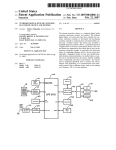
a derivative microcontroller; and
FIG. 8 shows a device in accordance with the inven
tion for emulating a microcontroller of the 80 C51 fam
ily.
BRIEF RECAPITULATION OF A KNOWN
MICROCONTROLLER
For the purpose of illustration FIG. 1 shows a block
diagram of the microcontroller (see also page 325 of the
cited reference). To the central bus 36 (8 bits) there are
successively connected:
an interface 38 for a serial data connection, compris
ing a clock connection SCLK. a serial data connec
tion SERDAT, and an interrupt connection SIO;
a latch circuit 40 and a buffer 42 for an 8-bit connec
tion;
a divider-by-SZ (44) and a counter 46 which receive
the internal clock frequency;
two program counters (48, 50);
a residential program ROM 54;
a program status word register 56;
two 8-bit connections with latches 58, 60 and buffers
62, 64;
an accumulator 66;
two temporary registers 68, 70;
an ALU (72) with a decimal adjust element 74;
an instruction register combined with a decoder 76;
a program counter 78;
a RAM address register 80;
a residential RAM (82) with data multiplexer, address
decoder, 8 registers, a register stack, an optional
second register bank, a data memory section;
a conditional branching logic block 86;
a control and timing element 88;
and a power-on-reset element 90.
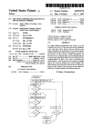
FIG. 2 shows the substitute for the part 54 of FIG. 1
in order to obtain the bond-out version. The address and
data lines are fed out and ?ve control lines are provided
also as extemal pins. This substitution thus concerns a
modi?cation of the circuit present on the substrate.
FIG. 3 shows the substitution in FIG. 1 for the part
“non-emulation", a microcontroller comprising the
54 which is necessary for the piggy-back version. The
standard number of connection pins is realized. The
steps now concern a sub-category of those of FIG. 2.
latter control can be realized internally by connection 65 When the steps of FIG. 2 have been implemented on the
to a ?xed potential.
Further advantages and embodiments are described
substrate, the steps of FIG. 3 concern only a different
herein.
not be connected in that case, or are connected to a
con?guration of the envelope: given bond pads need
5,062,034
5
?xed potential (for example, ground). Such a piggy
back version is known per se.
6
model (S.O.—small outline) in which exactly the re
quired number of connection pins is realized (a few
more than shown in FIG. 4). For example, the supply
.
DESCRIPTION OF AN EMULATION DEVICE
OF A MICROCONTROLLER OF THE 84 CXX
FAMILY
pins are not shown.
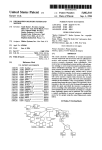
FIG. 5 shows a device in accordance with the inven
tion for emulating a microcontroller of the 84 CXX
FIG. 4 shows a block diagram of a microcontroller of
the type 84 CO0 which comprises a connection system
family, for example the 84C43. The parent microcon
troller 20 and the program memory 22 are shown in the
same way as in FIG. 1. If desired, the memory 22 may
for an external register. Therein, some elements are
provided in order to enable the use of this parent mi 0 be constructed as a random access memory (RAM)
crocontroller in a device for emulating a derivative
which forms part of a known emulation machine. This
microcontroller. The microcontroller, (element 20) is of
emulation machine may be, for example a PMDS/MAB
the bond-out version and comprises the following series
(Philips Microprocessor Development System/Mi
of standard pins (first series); the supply pins have been
omitted for the sake of simplicity;
?rst data connection P0 (8 bits);
second data connection P1 (8 bits);
third data connection P2 (4+1 bits);
testable input pin Tl;_
_
15
interrupt connection INT/IQ;
reset pin RESET;
oscillator input XTALl;
oscillator output XTALZ;
There is also provided the following second series of
connection pins for an external program memory 22 25
(EPROM of the type 2732 or 2716):
address connection A12-AOO so that a program
memory having a maximum number of SR ad
dresses can be used;
data connection D7-D0 which has the same width as 30
the connections P0, P1;
a memory activation connection Psi-l5; because this
program memory is used only in the read mode, the
above number of pins suffices. The program mem
ory can thus output data which are written into a
crocomputer Adapter Box) machine. This machine is
commercially available (not shown for the sake of brev
ity). Interaction therewith can take place in the same
way as described for the external registers in FIG. 4.
The parent microcontroller thus operates as a master
circuit.
Element 34 is the derivative microcontroller of the
type 8408. The additional derivative logic will be
described with reference to FIG. 6. A number of stan
dard pins are shown at the left:
the reset connection RESET;
the clock connections XTALI, XTAL2;
the data connection P2, together with a serial data
connection SDA for a so-called 12C bus;
the clock connection SCL associated with the 12C
bus; in the standard version this pin corresponds to
the pin T1; the 11C bus is implemented by means of
components which are described at the register
level in European Patent 51 332 and the corre
sponding U.S. Pat. No. 4,689,740 which is incorpo
rated herein by way of reference;
the data connection PI;
suitable register or register section in the microcon
the data connection Pl; only ?ve bit lines P10 . . . P14
troller 20 and which subsequently realize different
thereof are shown, the remainder is not used.
control functions.
The derivative microcontroller also comprises means
There is also provided an external 8-bit latch register
24. This register is connected to the data connection of 40 for driving a number of seven-segment display ele
ments. That is to say, twenty-four segment control pins
the memory 22 and is activated under the control of an
S??-SZS, whereby three seven-segment characters can
enable signal DXALE. A decoder 26 is connected to
be activated in parallel (the eighth bit is available for
the register 24. The 8-bit data in the register 24 is con
activating, moreover, a decimal stop). Four selection
verted into enable signals (in the decoder 26) for one or
signals BPO . . . BP3 (backplane 0 . . . 3) are also shown.
more of the data registers 28, 30, 32. These registers are
These signals enable selection between four different
connected in parallel to the data output of the memory
display elements, so that the l2-character capacity suf
22 so that they have a capacity of at the most 8 bits.
fices. The power supply for the display elements is
Further bidirectional connections of these registers to
received on pin VLCD. Finally, the derivative mi
the environment are also shown. The data registers 28,
crocontroller comprises an additional data connection
32 are synchronized by a signal M (an external
P2 which has a width of 4 bits. The pins and facilities
write control signal). As a result of the described orga
SDI-S23, BPI . . . 8P3, SDA, SCL, P2, VLCD form
nization, the registers 28, 32 can also be ?lled with data
the additional facilities in the derivative microcon
from the data connection D7-Dl. It is also possible to
troller. For other derivative versions more, fewer and
/or other facilities may be provided. The exclusive
omission of facilities with respect to the parent mi
control output m which is symbolically connected
crocontroller generally does not necessitate specific
only to the data register 32. The elements 24, 26, 28, 30,
emulation on the derivative microcontroller; however,
32 may be constructed as conventional 'I'I'L compo
in that case this emulation can be performed directly on
nents. The instructions MOV A, DX; MOV DX, A;
ANL DX, A; ORL DX, A internally required for the 60 the parent microcontroller. Alternatively, the parent
microcontroller may comprise given facilities which are
above activations are described in the cited reference.
not present in the derivative microcontroller. However,
The logic result of the last two instructions is stored in
each of the two microcontrollers always comprises a
the relevant register DX. Finally, the microcontroller
data processor element and adequate connection facili
also comprises a connection pin
1 for receiving an
ties and the derivative microcontroller comprises an
external interrupt signal. In the present simple example,
internal program memory (otherwise the emulation
however, this pin need not be used. The version of the
would be unnecessary). In given cases the entire inter
element 20 used in the present example has the type
nal program memory of the parent microcontroller can
number PCF4COOT; this is notably a 56-pin small
use the data registers 28, 32 as a data source for the data
connection D7-D?; to this end there is provided a
7
5,062,034
tive microcontroller of the 84 CXX family‘illustrating
additional functions specific to the derivative version.
The facility includes a generator 132 for the LCD sup
ply voltages. When a series connection of three resistors
and a parallel switch is connected between the supply
ory is always used.
The derivative microcontroller 34 can be emulated in
that it is connected to the parent microcontroller 20 as
follows. The connection Pi is connected to the data
connection D7 . . . DB of the parent microcontroller.
voltage VDD and the special supply voltage VLCD,
The derivative microcontroller can thus present itself to
the parent microcontroller in the same way as the regis
ter 24 in FIG. 4. Furthermore, the connection P1 is
LCD elements having an operating voltage of between
2 and 5 volts can be used. Element 128 comprises its
own oscillator, time control and voltage selection facil
suitable for communicating a number of control signals
with the parent microcontroller 20; the internal latch
register provided standard with this connection tempo
rarily stores these control signals. Connection pin P10
supplies the parent microcontroller with an external
interrupt signal EXDI. Connection pin P11 receives the
read control signals BXRD. Connection pin P12 re
ceives, in parallel with the external memory 22, the
enable signal PSEN. Connection pin P13 receives the
write control signal DXWR. These four control signals
have already been described with reference to FIG. 1.
Connection pin P14 receives the stop control signal
STFF. The stop control instruction can thus be exe
cuted; this instruction is executed in the parent mi
crocontroller in order to save energy (for example,
because the intended user environment comprises bat
tery power supply). This situation is communicated to
the derivative microcontroller by way of the signal
8
FIG. 6 shows an internal block diagram of a deriva
be dispensed with, because an external program mem
ity for the LCD elements. Element 130 comprises four
so-called backplane drive elements having four outputs.
Elements 120 . . . 122 (actually twelve) comprise regis
ter elements and multiplex elements for two segment
5
outputs (two display bits for each backplane). Elements
124 . . . 126 (again twelve) receive the power supply
from the element 128 so that they each drive two dis
play elements. The elements 120 . . . 122 are to be con
nected to the bus for the reception of the data to be
displayed with a width of 8 bits. To this end, they are
also selectively addressable. The adjustment of the dis
play mode to stationary (one backplanes or multiplexed,
as desired, on 2-4 different backplanes) can be realized
STFF, so that the derivative microcontroller can also
switch over to a stop mode. Switching between active
modes and stop modes is known per se. This signal
by means of permanent wiring in the same way as previ
ously described for the pin EMUL. in FIG. 5. The con
nection to the bus then corresponds to twelve different
addresses. The bus connections themselves are denoted
by the arrows 121, 123 and thus ensure the supply of
data and addresses. The further speci?cation of the bus
(width of data path and address path) has been omitted
STFF can be advantageously used notably for realizing
for the sake of simplicity.
a prototype (because the latter will also comprise the
FIG. 7 illustrates the two modes of operation for a
derivative microcontroller as described above. The
broken line 162 denotes the circuit accommodated on
above battery power supply).
Finally, the derivative microcontroller comprises an
the substrate. Block 150 represents the major part of the
emulation control connection EMUL. Under the con
functional processing elements shown in FIG. 1, nota
trol of a ?rst signal value on this connection, the deriva
bly the ALU, the residential program ROM, and the
tive microcontroller operates in the normal mode. In
elements for controlling the ALU which are connected
that case inter alia the processor, the program memory
in the organization between the ALU and the residen
and the random access memory provided on the chip
operate in the normal mode. Under the control of a 40 tial program ROM. Line 160 symbolizes the bus which
continues into block 158 in the closed state of the switch
second signal value on this connection, the derivative
154. The connection Pi is connected to the bus via a
microprocessor operates in the emulation mode and
buffer 156 and a latch register 152. Similarly, the ele
these components are disconnected. Instead, the ele
ment 2 is used as the program memory and the relevant
pans of the parent microprocessor 20 (which does not
include a program memory) are used for the processor
and the random access memory. The additional func
tional facilities (derivative logic) of the derivative ver
sion in the derivative microcontroller which are not
present in the parent microcontroller, however, should
remain operational. The above first value is, for exam
ple ground potential. In that case this signal can be
realized, for example by way of a connection to the
ground pin (GND, not shown in FIG. 5) already pro
ments 166, 168 associated with the connection P1 are
connected to the part of the bus situated above the
switch 154. It is alternatively possible to replace the
combination 152/156 by an organization which includes
a bidirectional buffer, the devices then being activated
by the signals EXWR and m (see FIG. 5). Element
158 symbolizes the additional functional processing
facilities for the derivative version, so in this case nota
bly the elements shown in FIG. 6, the connection means
for the serial 12C bus described above, and also the
connection P3.
The switch 154 is opened and closed under the con
vided on the chip, so that no additional connection pin 55
trol of the signal on the connection pin EMUL. When
on an envelope is required. This has only the drawback
that the relevant specimen of the derivative micro
processor can no longer be used as an independent com
the switch 154 is closed, therefore, all functional pro
cessing elements of the microcontroller are operational.
When the switch 154 is open, only the additional deriva
ponent in applications other than emulation. This con
nection will usually be realized by way of a speci?c 60 tive logic 158 is operational as well as the elements
which are required for the emulation mode. Operational
wired connection between two bond pads.
is to be understood to means herein that the interaction
Internal emulation control may be realized by way of
with the environment takes place in the usual manner.
a mask connection to one of two standard potentials (i.e.
power supply and ground). The mask con?guration for
realizing the conductor tracks is then adapted. This
In the emulation mode the interaction between the
65 block 150 and the environment is interrupted; inside the
lier production step than when use is made of an emula
block 150, however, further actions may still take place.
It is notably for this reason that the switch 151 is pro
tion control pin or bond pad.
vided; this switch is opened together with the switch
means that the function must then be de?ned in an ear
5,062,034
10
154. Any signals supplied by the block 150 are then
gram memory not intended for emulation can substitute
blocked as far as the environment is concerned. FIG. 7
for one another or supplement one another;
shows the connection PI and associated parts of the
elements which are active for the emulation. This ?gure
also concerns (as shown in FIG. 5);
the reset connection (element 90);
the oscillator connection XTALZ (and hence the
element 88).
The other standard functions are performed by the
'
selection signal for sel_ection between internal/exter
nal program memory (EA);
a reset signal (RESET);
a supply terminal (V DD) and a ground terminal
(GND) which, of course, are present in all circuits
shown.
The relevant bond-out version has the following fa
cilities for the emulation:
an 8-bit latch circuit (104) which is controlled by the
parent microcontroller so that they need not be active
in the derivative microcontroller. In given cases the
division may be such that given facilities in the deriva
tive microcontroller remain active, even if they could
signal ALE;
be replaced by similar facilities in the parent microcon
troller. An example in this respect is the situation where
the parent microcontroller comprises a data memory
(RAM), but the derivative microcontroller comprises a
a program memory (106) (EPROM) or the read/
write memory of the emulation machine; this memory
can receive addresses having a width of 16 bits; the data
has a width of 8 bits.
a buffer/gating element 108 which receives a number
larger RAM. In that case a choice can be made be
tween: the use of the entire parent RAM plus a part of
the derivative RAM and the use of only the entire de
of external signals M1. M2, INTR, EXl, INTD and
which selectively conducts these signals.
The following connections are also provided:
rivative RAM. The additional registers in the derivative
a multiplexed line for the least-signftcant address bits
microcontroller can usually be used as locations of the
for the program memory as well as for the data bits
random access memory (RAM) of the parent microcon
(EAD7 . . . I);
troller.
a multiplexed line for the most-signi?cant address bits
The facility in one of the two microcontrollers will be 25 and the output signals of the buffer/gating element 108
selected according to the nature of the facility and the
(EA8 . . . EAIS);
architecture.
an enable signal P§E§E which is especially intended
As is shown, the switch 154 can again be situated in
for the emulation memory (deviates from PSEN);
the bus. In given cases the deactivation of the communi
a control signal which indicates whether the parent
cation with the block 150 can be realized in a different
microcontroller is in the standby (idle) or power-down
manner. For correct connection of the control signals
state; (in these states the program is not further exe
cuted, compare the stop mode in FIG. 2);
164. When the switch 154 is opened, the switch 164 is
a machine selection signal (Cl/INTD) which indi
closed. The control signals are then communicated with
cates whether the ?rst, the second or a next cycle of a
the connection element 170. This element provides
multi-cycle instruction is the current one; during the
suitable buffering and is also connected to further parts
first cycle the opcode appears; during the second or
further cycles operands may appear, or they may be
of the circuit, for example in order to activate read,
write or stop operations and for conducting an interrupt
provided for given prolonged executions such as multi
signal. The latter connections have been omitted for the
plication;
sake of brevity. For the sake of simplicity, the realiza 40 an interrupt acknowledge signal (IN I A) which, how
tion control means by internal wiring on the chip has
ever, is not used in this context;
been omitted at the lay-out level.
a multiplexed address/data signal (RSAD7 . . . I)
having a width of 8 hits;
DESCRIPTION OF AN EMULATION DEVICE
the external read (m) and write (R§WR) si nals
FOR A MICROCOMPUTER OF THE 80C5l
which correspond to the signals DXRD, ?XWR of
FAMILY
FIG. 2;
FIG. 8 shows a device in accordance with the inven
a latch register enable signal (RSALE);
tion for emulating a microcontroller of the 80C5l fam
a “memory/special" signal (RAM/m). which indi
cates whether the data is intended for the random access
ily. The main part of the parent microcontroller 80C5l
memory of the derivative microcontroller or for a regis
B.O. (=bond-out) is described in the cited reference,
ter or registers having a special function included
pa es 70-121. However, the connections RSAD'J. . . l.
(pins P10 . . . 14) there is also provided a second switch
therein;
. . I?TA described hereinafter are added.
The parent microcontroller 100 comprises the fol
lowing connections:
a data connection PI (8 bits);
a data connection P1 (ditto; however, it is not used in
?nally. there may also be provided a small number of
synchronization handshake signal connections (WT,
55
M1) for an interrupt mechanism; (as a result of this
facility, the instant of appearance of an interrupt signal
need not be subject to restrictions which could be
caused by timing relations between the parent mi—
a data connection P2 (8 bits);
crocontroller and the derivative microcontroller).
a data connection P3 (8 bits); in addition to the func
tion of data connection, the bit lines thereof have the 60 The derivative microcontroller 102 is shown in two
versions which differ as regards their additional deriva
following alternative functions: serial in/out; external
tive logic. In the first derivative version, only a serial
interrupt (2 X); external timer (2 x); and external write
bus connection for an IZC system is provided above the
(3.6) and read (3.7)-synehronization; in the emulation
elements of the parent microcontroller. The derivative
situation only the latter two bit lines are used;
the present embodiment)—8 bits;
address latch enable signal (ALE);
two clock connections XTALI, 2;
enable signal for the program memory (RS-m). so
that the internal program memory and an external pro
65 microcontroller has the following connections:
two connection pins for power supply (V DD, GND);
two clock connection pins (Bl-l2) for synchroniza
tion by means of clock signals from the parent mi
5,062,034
11
tor crystal;
12
received which can be converted into a digital signal in
the derivative microcontroller. To this end, the analog
crocontroller instead of by means of an external oscilla
.
a data connection having a width of 8 bits (PD) which
signals can be received on a multiplexed AD converter.
is bidirectionally connected to RSAD7 . . . H of the
The channels can also be used for digital signals in
which case they can be bidirectionally active;
a one-bit synchronization signal (STADC) for initial
parent microcontroller;
a data connection (P2) which has a width of 8 bits and
the one-bit connections P20-P27 of which are used as
izing the above analog~to~digital conversion (strobe);
two reference voltage connections (V REF+,
follows:
P20: read control signal for the special function regis
VREF-) which are required in order to realize said
analog-to-digital conversion;
ter (SFRRD);
P21: ditto, write control signal (SFRWR);
P22: ditto, enable signal (SFRALE);
two supply voltages (AVSS, AVCC) which are pro
vided especially for the AD conversion;
P23: selection signal for making a selection between
the random access memory and special function
by pulse-width modulation;
two outputs for signals (PWMD, PWMI) analogized
15
register (RAM/511i);
P24: the enable si nal for the external program mem
ory 106 (P ENE) which synchronizes (bidirection
ally) the status of the parent microcontroller and
that of the derivative version;
‘
__ __
P25: the signal standby/stop mode (IDL/PD) of the
parent microcontroller;
P26: a stop bit which is formed by the emulation
machine in order to stop the derivative/parent
EWN, an activation signal for the watchdog timer.
The following connections are not used:
the clock signal output XTAL2;
the address register enable line ALE;
FA, an external activation signal; see also the parent
microcontroller;
the line P§EN for an external program memory (see
the parent microcontroller).
microcontroller, for example for the static reading
The activation and deactivation of the relevant func
crocontroller this connection has the previously
to the connection EMUL; this can be internally real
ized, for example in the manner corresponding to FIG.
7. When the additional facilities for the derivative mi
crocontroller are continuously activated (for example,
of register contents therein. On the parent mi 25 tions can again be realized by means of a signal applied
described double function. The signal INTD can
be received from the buffer 108.
P27: this signal makes a selection between the two
versions of the derivative microcontroller (83C652
and 83C552, respectively). The relevant signal can
be obtained again by way of a selective bond con
nection as previously described for the signal
EMUL in FIG. 5;
only the pins P36 and P37 of the data connection P3,
having a width of 8 bits, are connected parallel to the
pins P36 and P37, respectively, of the parent microcon
troller. There are also provided a air of connection
pins which correspond to the pins
, W of the
parent microcontroller in order to realize a synchroni
zation handshake for an interrupt signal from the deriv
ative microcontroller.
The other connections are absent or not used for
the switches 151/154 are closed and the switch 164 is
open) by way of a voltage applied via a wire between
two bond pads, it will no longer be necessary to provide
a special pin on the envelope, so that the enclosed mi
crocontroller can be used in the same way as the~stan
dard version, that is to say in any appropriate user envi
ronment.
A further possible use of a derivative microcontroller
of the above type is as a peripheral apparatus of the
parent microcontroller. In that case the internal pro
gram memory of the parent microcontroller can be
activated again. Only the added functions of the deriva
tive microcontroller are then operational. A derivative
microprocessor whose arithmetic and logic unit and/or
emulating this version of the derivative microcon
internal program memory are faulty can thus still be
45 used; the parent microcontroller then acts as a stand-in
troller.
In the second derivative version a number of further
for the faulty functions.
facilities are realized which are embodied in relevant
What is claimed is:
functional elements. i.e. AD conversion (from voltage
l. A device for emulating a microcontroller of a stan
to bit pattern), DA conversion (from bit pattern to pulse
dard, non-bond-out type having standard pins, and a
length modulation), additional connections P4, P5, a 50 standard processor element, the claimed device com
counting mechanism for events (event counter), a
prising:
watchdog timer, and the previously mentioned 12C
connection. In addition to the previously described
connections, the present version also comprises the
following connections (only a few additional connec 55
tions of the parent microcontroller are used; however,
these were already provided in the present bond-out
version):
a reset connection for the input/output mechanism
(RESl/O) which is bidirectionally connected parallel to
the reset connection of the parent microcontroller;
a clock signal input (XTALI) which is controlled, via
a buffer stage (110), by the clock signal output
(XTALZ) of the parent microcontroller;
two data connections P1, P4 having a width of 8 bits; 65
the remaining 6 bits of the Shit data connection P3;
a data connection (P5) having a width of eight chan
nels; on each of these channels an analog voltage can be
a. an external program memory;
b. a bond-out parent microcontroller, with respect to
which the external program memory is external
and which comprises:
i. a ?rst plurality of pins, corresponding to the
standard pins, for executing input/output opera
tions;
ii. a second plurality of pins for exchanging data,
addresses, and control signals with the external
program memory;
iii. a third plurality of pins for exchanging control
signals with external hardware;
iv. a processor element;
v. means for communicating between said proces
sor element and said first, second, and third plu
rality of pins;
5,062,034
13
14
c. a derivative non-bond-out microcontroller of the
a. an external program memory, which is external to
standard nombond-out type, with respect to which
the parent microcontroller and any microcon
troller to be emulated;
b. a derivative non-bond-out microcontroller of the
the external memory is external, comprising:
i. a processor element;
ii. an internal program memory;
standard non-bond-out type, comprising:
iii. communication means for exchanging informa
tion between the processor element of the deriv
ative microncontroller and the internal program
memory of the derivative microcontroller;
iv, derivative logic, not present in the parem mi. 10
crocomrouer;
v. a plurality of pins, which are the standard pins,
i. a processor element;
ii. an internal program memory;
iii. communication means for exchanging informa
tion between the processor element of the deriv
ative microcontroller and the internal program
memory of the derivative microcontroller;
“1- dcnvatlvc logic. "0‘ Firm!" in the Parent mi
forming;
crocontroller;
A. a ?rst data connection coupled to the external 1 5
‘’~ fa pllfl'allty of Pins, Whlch 8"! lhc slandal'd Pins,
program memory, in parallel with the second
0111111181
plurality of pins of the parent microcontroller;
I
A. a ?rst data COBIICCUO: coupled to the external
and
program memory; an
B. a second data connection coupled to the third
plurality of pins of the parent microcontroller, 20
and including at least one control pin coupled
3- a second danf °°ml¢m1°n lflcludilng 8‘ least
one comm] PIn coupled with 581d exlcmal
_
PYOETPm mcmory; and
_
will, said enema] program memory’ in parap
M with at least one corresponding comm] pin
vi. emulation control'means which assumes a state
during emulation, in which state the emulation
of the second plurality of pins of the para“
microcommner. and
control means deactlvates the communication
means of the derivative microcontroller;
vi. emulation control means which assumes a state 25 th‘ claimed Parent. microcontroller ‘comprising-1
during emulation, in which state the emulation
c- P bond'out mlcfocomrollcr wh'ch cml'll’mest
control means deactivates the communication
1' *‘ ?rst plufahty °f Pms’ concspondmg ‘0 the
means of the derivative microcontroller, so that
__ standard Pmsi
during
emulation
A. the processor
30
mi-
u. :d‘siecond
plugalitytoflpms it!” expiharlilgmg
datai
rm’ an confo 5'3" 5 “_’|
‘ “ml-"a
crocontroller, and the external program memmy an activated “mead of the processor db
mm, and internal program memory of the
derivative microcontroller;
35
Program memory’ mParf‘ncl ‘fwth ‘he ?rs‘ dam
connection of the derivative microcontroller, the
secondl plurality of pins including at least one
contro pin corresponding to and coupled to the
element, of the parent
B_ the ?rst mummy of pins of ‘he parent mi_
_
_
_
external program memory, in parallel with the at
crocommuer act as standard pins of ‘he deriw
least one control pm of the second data connec
ative microcontroller, "Id
tion of the derivative microcontroller;
C. the derivative logic is activated and con.
m‘ a mud ph‘lhmmy of Plum; exchangmg comm]
.
‘gnal
'
.
.
. .
.
.
iv‘:
t f r a lat
.
'
'
—
elcmflrrreglsmr enable s‘gml'
-
whereby the parent microcontroller emulates the derivaugcalcgocqmroilmi' . 1 h .
. h e h‘C\d'lCCl o lcaimf w elf];
.
comprising two read and write control pins and
45
_
’
tive microcontroller, the third plurality of pins
tive microcontroller performs functions spe-
ci?c to it which cannot be performed in the
parent microcontroller;
.
and coupled
‘Y'th the second dun conmgmn of {he denim‘
.
u
ware
s‘.
parent microcontroller, whereby the deriva.
s w‘
ternal
nected to the communication means of the 40
9
v_ means for communicating between said pr°ces_
sor element and said ?rst, second, and third plu
_
“my of pins;
a‘ t e t ‘r p “Ya "y o pms o t c parent ‘Pm-000"‘
so that during emulation, under control of the emulation
troller comprises a stop output for supplying a stop 50 Comm! means:
control s'glmli
_
d. the processor element, of the parent microcon
b. the emulation control means further comprises a
"on", and the cum program memory are new
m0P comm] ‘lament comm?“ ‘0 ‘he ‘FOP O'J‘P‘n'
vated instead of the processor element and commu
tlle SPOP ccfmrol elemem bemg for causmg ‘he dc‘
nication means of the derivative microcontroller;
rivative microcontroller to assume a stop mode.
55
and
3- The dfvlce of claim 1 when"!
1\) ‘h: microcontroller of the 93PM non'bQnd'om
e. the ?rst plurality of pins of the parent microcon
troller act as the standard pins of the derivative
type has exactly one set of pins_all of which are
standard pins. which Standard Plns "e sifmdm'd'
tzed in their number, Placement. Ind ?mCllO?S;
60
b) the ?rst plurality of ptns corresponds to all Of the
microcomrouer; and
l‘. the derivative logic is activated and connected to
the communication means of the parent microcon
troller, whereby the parent microcontroller uses
standard pins; and
c) the derivative microcontroller has exactly one
plurality of pins, which are the standard pins.
4. A parent microcontroller for use in a device for 65
emulating a microcontroller of a standard, non-bond
out type having standard pins, and a standard processor
element, the device including:
the derivative microcontroller to perform func~
lions speci?c to the derivative microcontroller
which came! be performed in the parent mi
crocontroller;
‘
whereby the parent microcontroller emulates the deriv
ative microcontroller.
5. The parent microcontroller of claim 4 wherein
15
5,062,034
16
pin of the second plurality of pins of the parent
a. the third plurality of pins of the parent microcon
troller comprises a stop output for supplying a stop
microcontroller; and
'
h. emulation control means which assumes a state
control signal;
during emulation, in which state the emulation
b. the derivative microcontroller further comprises a
stop control element connected to the stop output,
the stop control element being for causing the de
control means deactivates the communication
means of the derivative microcontroller, such that:
i. the processor element, of the parent microcon
troller, and the external program memory are
activated instead of the processor element and
internal program memory of the microcon
rivative microcontroller to assume a stop mode.
6. A parent microcontroller as claimed in claim 4,
characterized in that it comprises a pair of synchroniza
tion handshake connections for interrupt signals for
connection to corresponding synchronization hand~
shake connections of said derivative microcontroller.
troller;
. the first plurality of pins of the parent microcon
troller act in place of the standard pins of the
7. The microcontroller of claim 4 wherein
a) the microcontroller of the standard non-bond-out
type has exactly one set of pins all of which are
microcontroller; and
iii. the derivative logic is activated and connected
to the communication means of the parent mi
standard pins, which standard pins are standard
crocontroller, whereby the derivative microcon
ized in their number, placement, and functions;
troller performs functions speci?c to it which
b) the ?rst plurality of pins corresponds to all of the
cannot be performed in the parent microcon
standard pins; and
troller;
c) the derivative microcontroller has exactly one 20
whereby the parent microcontroller emulates the deriv
plurality of pins, which are the standard pins.
ative microcontroller.
8. A non-bond-out microcontroller of a standard,
9. The derivative microcontroller of claim 8 wherein
non-bond-out type having standard pins, and a standard
a. the third plurality of pins of the parent microcon
processor element, for use as a derivative microcon
troller in a device for emulating the derivative mi 25
crocontroller. the device including:
b. the emulation control means further comprises a
stop control element connected to the stop output,
a. an external program memory, which is external to
both the derivative microcontroller and a bond-out
the stop control element being for causing the de
parent microcontroller; and
. such a bond-out parent microcontroller, which 30
wherein the emulation control means comprises:
i. a ?rst plurality of pins, corresponding to all of the
connection means for control signals, which connec
tion means is
35
tion control means and
iii. a third plurality of pins for exchanging control
signals with external hardware;
11. A derivative microcontroller as claimed in claim
8 or 9, characterized in that said emulation control
means is mask programmed.
12. The derivative microcontroller of claim 8
wherein the emulation control means comprises a con
nection external to the derivative microcontroller.
iv. a processor element;
v. means for communicating between said proces
sor element and said ?rst, second, and third plu~
rality of pins; the claimed microcontroller being
of the standard non-bond-out type and compris
45
13. The derivative microcontroller of claim 8,
wherein the derivative microcontroller is an inte
c. a processor element;
grated circuit; and
d. an internal program memory;
further comprising means for providing a logic sig
nal, for preventing the emulation control means
e. derivative logic. not present in the parent mi
crocontroller;
from assuming the state.
i‘. communication means for exchanging information
between the processor element of the microcon
troller and the internal program memory of the
.
14. The derivative microcontroller of claim 13
wherein the providing means includes a source, internal
to an envelope of the integrated circuit, for the logic
microcontroller;
g. exactly one plurality of pins, which are the stan
dard pins, for forming, during emulation:
i) activated in response to said state of said emula
ii) coupled with a subset of the pins of the deriva
tive microcontroller.
program memory;
ing:
rivative microcontroller to assume a stop mode.
10. The derivative microcontroller of claim 8 or 9
includes:
standard pins, for executing input/output opera
tions;
ii. a second plurality of pins for exchanging data,
addresses, and control signals with the external
troller includes a stop output for supplying a stop
control signal;
signal.
55
i. a ?rst data connection for coupling with the
external program memory. in parallel with the
second plurality of pins of the parent microcon
troller; and
‘
15. The microcontroller of claim 8 wherein
a) the microcontroller of the standard non-bond-out
type has exactly one set of pins all of which are
standard pins, which standard pins are standard
ized in their number, placement, and functions;
b) the first plurality of pins corresponds to all of the
standard pins; and
ii. a second data connection for coupling with the
third plurality of pins of the parent microcon
c) the derivative microcontroller has exactly one
plurality of pins, which are the standard pins.
troller, and including at least one control pin for
coupling with said external program memory, in
parallel with at least one corresponding control
Q
65
I
I
O
'