1
DATA SPACE
PROGRAM SPACE
PAGE 0
PAGE 1
PAGE 2
PAGE 3
PAGE X
FFFF
FFFF
FS1
FS3
FS5
FS7
C000
C000
FS0
FS2
FS4
FS6
NOTHING MAPPED
8000
8000
COMMON
MEMORY
ACROSS ALL
PROGRAM
PAGES
Execute
from
here
NOTHING MAPPED
NOTHING MAPPED
NOTHING MAPPED
NOTHING MAPPED
4000
4000
CSBOOT1
CSBOOT1
CSBOOT1
CSBOOT1
CSBOOT0
CSBOOT0
CSBOOT0
CSBOOT0
2000
0000
1000
SYSTEM RAM & I/O
0000
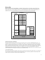
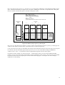
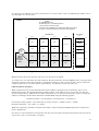
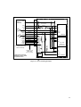
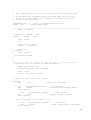
Figure 21 Memory positions after step 2 of memory swap
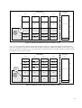
Next, we write to the PAGE register, to the swap bit location a value of 1. This action changes the system location
where the code appears to the microcontroller moving FS0 to 0x0000 and CSBOOT to 0x8000 as shown below. After
this write operation is complete, the very next instruction is fetched from FS0. Execution continues from FS0 until the
next time the system is powered down.
DATA SPACE
PROGRAM SPACE
PAGE 0
PAGE 1
PAGE 2
PAGE 3
CSBOOT3
CSBOOT3
CSBOOT3
CSBOOT3
CSBOOT2
CSBOOT2
CSBOOT2
CSBOOT2
PAGE X
FFFF
FFFF
C000
C000
Execute
from
here
COMMON
MEMORY
ACROSS ALL
PROGRAM
PAGES
CSBOOT1
CSBOOT1
CSBOOT1
CSBOOT1
CSBOOT0
CSBOOT0
CSBOOT0
CSBOOT0
8000
FS1
FS1
FS1
NOTHING MAPPED
8000
FS1
4000
4000
FS0
FS0
FS0
FS0
1000
SYSTEM RAM & I/O
0000
0000
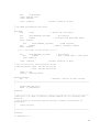
Figure 22 Memory locations after step 3 of memory swap
20