1
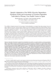
National Semiconductor
Application Note 1376
Lee Sledjeski
April 2005
1.0 Introduction
FPGA allows the FPGA I/O to be programmed at the minimum CMOS drive level of about 2 mA. Reducing the drive
level lowers the dynamic currents within the FPGA curbing
the generation of SSO noise. Noise generated in the I/Os on
a FPGA can corrupt the analog performance of FPGA PLLs
or other system analog resources.
The Altera Cyclone or Xilinx Spartan are good examples of
economical FPGAs intended for low to medium end applications. They do not contain dedicated serialization or deserialization circuitry for high-speed communications limiting the
maximum data rate. This makes the Cyclone and Spartan
good candidates for an external serial interface. Using a
SerDes external to an FPGA allows an entire multi-byte
parallel interface to be condensed to one or more highspeed signal pairs for economical transmission across system interfaces. Before and after measurements of the SSO
noise on a Cyclone FPGA will help to quantify the improvements made by the change in the FPGA programmed I/O
current drive.
A critical issue with any FPGA (Field Programmable Gate
Array) design is Simultaneous Switching Output (SSO)
noise. SSO noise, also known as ground bounce, is a result
of large instantaneous changes in current across the power/
ground inductance of the integrated circuit. This potential
problem becomes more and more serious as the number of
active high-drive LVCMOS outputs on a FPGA design increases. In large FPGAs with several synchronous parallel
interfaces this phenomenon can result in poor system performance or intermittent data errors.
This application note highlights how using external SerDes
in conjunction with minimum current drive FPGA I/O can
reduce FPGA’s internal noise and reap the benefits of a
serial interface across the system. This may allow designers
to use low end FPGAs with external SerDes to reduce cost
and still have high analog performance.
The FPGA SSO noise is minimized by using the lowest drive
current from the FPGA and reduces the parallel bus to a
single differential signal. LVCMOS outputs from the FPGA
are unsuited for driving over long interconnects or at high
data rates. Upgrading the parallel interfaces with an external
Serializer/Deserializer (SerDes) interface to the FPGA will
reduce SSO noise and improve the overall system performance. The close proximity of the external SerDes to the
2.0 Test Setup for Simultaneous
Switching Output Noise
The FPGA/SerDes evaluation test setup is shown in
Figure 1.
20146101
FIGURE 1. DS92LV16 SerDes and Cyclone FPGA Test Setup
© 2005 National Semiconductor Corporation
AN201461
www.national.com
AN-1376 External Serial Interface Reduces Simultaneous Switching Output Noise in FPGAs
AN-1376
External Serial Interface
Reduces Simultaneous
Switching Output Noise in
FPGAs
AN-1376
2.0 Test Setup for Simultaneous
Switching Output Noise (Continued)
used for the interface would depend upon the device selected, additional required functionality, and other layout constraints. For the best and most consistent AC performance,
all the FPGA — SerDes interconnects should be selected
from a single I/O bank.
2.1 TEST SETUP SCHEMATIC
Figure 2 shows an example of a system implementation
using the Cyclone and DS92LV16. The specific Cyclone I/Os
20146102
FIGURE 2. Cyclone and DS92LV16 Connections
www.national.com
2
also contains loop back test capability for testing line and
local interfaces. The Serializer and Deserializer operate independently with separate clock, enable, and power down
pins.
2.2 COMPONENT INFORMATION
2.2.2 Altera Cyclone FPGA
Table 1 shows the Cyclone device family and features. After
selecting an FPGA to handle the logic and processing requirements of the application, the designer may chose to
add an external SerDes due to system interface requirements. The FPGA choice depends on the end application
requirements; the DS92LV16 can be effectively used with
any FPGA density or architecture.
2.2.1 National DS92LV16 SerDes
Figure 3 shows the block diagram for the DS92LV16 SerDes. The serializer takes 16-bits of parallel LVCMOS data
and translates it into a serial stream with embedded clock.
The serial data stream is output as a Low Voltage Differential
Signaling (LVDS) signal with a maximum speed of 1.44
Gbps across cables or backplanes.
The deserializer takes the differential LVDS signal and translates it back into 16-bit parallel LVCMOS data. The device
20146103
FIGURE 3. DS92LV16 Block Diagram
TABLE 1. Device Features
Feature
LEs
M4K RAM Blocks (128 x 36 bits)
Total RAM Bits
PLLs
Maximum User I/O Pins
EP1C3
EP1C4
EP1C6
EP1C12
EP1C20
2,910
4,000
5,980
12,060
20,060
13
17
20
52
64
59,904
78,336
92,160
239,616
294,912
1
2
2
2
2
104
301
185
249
301
The following test was conducted with the FPGA to
DS92LV16 parallel bus clocking at 80 MHz and the LVCMOS
output drive current of the FPGA set to either 24 mA or 2 mA.
This will allow for the observation of SSO noise and other
noise related effects on the parallel bus.
1. Simultaneous Switching Outputs — Switched 16 FPGA
outputs simultaneously while monitoring a “quiet output”
for ground bounce on the FPGA evaluation board.
3.0 Simultaneous Switching
Output Noise
SSO noise, as the name implies, is the result of internal and
external circuitry switching at the same time. The cumulative
effect of all this switching current passing through power and
ground inductance is device-generated noise. This noise is
visible on non-switching outputs as internal movement in the
ground or power network.
3
www.national.com
AN-1376
2.0 Test Setup for Simultaneous
Switching Output Noise (Continued)
AN-1376
3.0 Simultaneous Switching
Output Noise (Continued)
2.
Figure 4 shows the level of noise that can result from only 16
LVCMOS I/Os switching at the same time.
Clock Output Jitter — Switched 16 FPGA outputs simultaneously while monitoring a FPGA clock output for jitter.
20146105
FIGURE 4. Active Output Transitions and “Quiet Output” (bottom), SS Data, 24 mA
voltage of switching logic. The dynamic shift in supply voltage will cause changes in the switching characteristics of
internal signals and reduce the performance of other more
sensitive analog circuitry.
In addition, the output signal also shows ringing and
undershoots.
The upper waveform (CH1) is the active switching transition
repeated on 15 additional LVCMOS FPGA outputs driven at
24 mA. There is a visible 600 mV undershoot present just
after the waveform falling edge. As expected, the bottom
“quiet output” waveform (CH2) tends to follow this pattern
highlighting an internal ground movement of ± 500 mV
around the true board ground. This internal noise in the
ground and power systems can dynamically alter the supply
20146106
FIGURE 5. Active Output Transitions and “Quiet Output” (bottom), SS Data, 2 mA
Figure 5 shows the quiet and switching waveforms with the
FPGA programmed for 2 mA (minimum) current drive. The
upper waveform (CH1) is the active switching transition repeated on 15 additional LVCMOS FPGA outputs. Compared
to the previous waveform, the 2 mA drive current results in
www.national.com
slower transition times and greatly reduced undershoot relative to external ground. Monitoring the signal on a quiet
output (CH2) shows the improvement on the internal ground
as well.
4
PLL analog performance. In addition to the reduction in
FPGA performance, analog devices located adjacent to the
FPGA will also be affected by the increase in ground noise.
The following series of waveforms (Figure 6) show how a
reduction in drive strength can improve the signal integrity
and lower the jitter seen on FPGA output signals.
The FPGA drive current reduction improves the signal integrity and lowers the jitter of output Clock signals. The noise on
the clock signal is another indication of diminished FPGA
20146108
20146107
Reducing the FPGA programmed drive to 2 mA results in a tightly controlled
clock waveform.
With 24 mA of drive programmed into the FPGA outputs, large excursions
outside the supply rails are clearly visible.
20146110
20146109
Rising Edge Magnification: This view shows how a reduced 2 mA drive
current maintains good signal integrity and exceptionally low (∼50 ps) jitter.
Rising Edge Magnification: This view shows greater than 200 ps of clock jitter
in the FPGA output that is a result of the increased drive current.
FIGURE 6. 24 mA Drive vs 2 mA Drive for FPGA Output Clock Signal Integrity and Jitter
The reduction in jitter will improve analog performance of
adjacent components like the DS92LV16. Starting with a
clean clock source means that significantly reduced jitter
within the PLL bandwidth will allow for enhanced high-speed
signal integrity.
By reducing the FPGA interconnect to short-to-point topology, the low drive (2 mA) setting can efficiently and cleanly
drive the LVCMOS interconnect into the LVDS SerDes. Programming to the low drive setting reduces the noise generated by the FPGA and reduces system EMI. Figure 7 and
5
www.national.com
AN-1376
3.0 Simultaneous Switching
Output Noise (Continued)
AN-1376
3.0 Simultaneous Switching
Output Noise (Continued)
4.1 External SerDes Reliability
The main function of any SerDes chipset is to translate data
originating from a wide parallel bus into one or more serial bit
streams and to convert the data back a wide parallel bus at
the receiving end. With the system improvements SerDes
devices bring, one of the first questions system designers
may ask is how long the interconnect between the serializer
and the deserializer can be that will still ensure error-free
data transfer.
Figure 8 clearly show undershoot and overshoot is completely eliminated and noise reduction achieved with low
drive FPGA programming.
To find out the answers to questions of “How far?” and “How
fast?” a type of testing called BER or Bit Error Rate Testing
is done on the serial interface.
Figure 9 shows the eye diagram at the DS92LV16 receiver
after 1m of CAT5 cable. This diagram shows the wide open
eye possible with inexpensive CAT5 cable running at a data
rate of almost 1 Gbps. The maximum data rate of the
DS92LV16 is approximately 1.5 Gbps.
20146111
FIGURE 7. 24 mA FPGA Output +4" Trace with PRBS
Data
20146114
FIGURE 9. Eye Diagram after 1m of CAT5 Cable
A related example of this type of testing is shown below. As
depicted in Figure 10, a BER transmitter provided 18-bit
wide PRBS (215-1) and a BER receiver received 18-bit wide
PRBS (215-1). The DS92LV18 transmitter serialized the sequence and sent it across a cable assembly; the DS92LV18
receiver then de-serialized the data, and sent the 18-bit wide
PRBS pattern back to the BERT for analysis. Configuring the
test setup in this manner allows the maximum operating
frequency to be determined for each cable length. The maximum operating frequency of this system is defined as the
maximum frequency of the device transmitter clock (TCLK)
at which the device receiver misinterprets zero out of 1012
data bits. This equates to the bit error rate of less than 1 x
10−12. The test was conducted at room temperature and the
power supply voltage for both devices was set to 3.3 volts.
For a DS92LV18 SerDes the TCLK frequency equates to
1/20th of the high-speed serial data rate. For example, at the
chipset maximum TCLK of 66MHz the serial data rate is
running at a speed of 1.32Gbps.
20146112
FIGURE 8. 2 mA FPGA Output +4" Trace with PRBS
Data
4.0 Benefits of Using External
SerDes
LVCMOS outputs from the FPGA are unsuited for driving
over long interconnects or at high data rates. To address
these system demands and to reduce the number of signals
at backplane or cable interfaces, SerDes devices with low
voltage differential signaling (LVDS) technology are often
employed.
www.national.com
6
AN-1376
4.0 Benefits of Using External SerDes
(Continued)
20146115
FIGURE 10. DS92LV18 SerDes BER Test Setup
Based on the BERT results, the DS92LV18 can be used in
short to medium length cable interface applications. If employed to move data between two points across a generic
category 5 cable, it can operate at its highest operating
frequency (66 MHz) for cable lengths up to 10 feet. For lower
operating frequencies, it can transmit error free data over
cables longer than 50 feet. Shielded cables with lower nominal attenuation paired with connectors rated for gigabit operation enable you to make longer high-speed, error free
connections.
Even though the speeds have increased dramatically, the
serial interface can transfer data at a rate and distance just
not possible with a parallel interface. In order to accommodate Gigabytes of data 32, 64, or even 128-bit parallel bus
designs have been implemented. This resulted in massive
routing bottlenecks at cable assemblies, memory board, and
backplane interfaces. These performance-limiting issues
were addressed when the parallel interfaces were replaced
with one or more high-speed serial interfaces. This architecture shift has enabled system performance, packaging, and
features that could not otherwise have been achieved.
4.2 External SerDes With Pre-Emphasis Feature
Even at the lower data rates used in parallel architectures, a
factor limiting transmission distance has always been the
electrical losses of the transmission media. Serial architectures have progressed to address the dielectric and skin
effect loss issues associated with high-speed design in several ways. In order to achieve high-speed reliable data transmission across cables up to 50 feet long something must be
done to compensate for the high frequency loss in the cable.
Pre-emphasis is a circuit design technique that adds high
frequency energy to the transmitter output signal, negating
the loss incurred during data transmission across the medium. The National Semiconductor SCAN921821, a dual
18-bit Serializer, uses 6 dB of pre-emphasis to maintain
robust, error-free communication across 50 feet of cable.
This added feature increases the reach of LVDS SerDes by
up to 5x at > 1 Gbps serial data rates.
7
www.national.com
AN-1376
4.0 Benefits of Using External SerDes
(Continued)
20146116
Measured after 15m of Infiniband Cable at the Input of the DS92LV18 Receiver; fTCLK = 66 MHz (1.32 Gbps); No Pre-emphasis
FIGURE 11. Eye Diagram measured after 15m of Infiniband Cable at the Input of the DS92LV18 Receiver;
fTCLK = 66 MHz (1.32 Gbps); No Pre-emphasis
www.national.com
8
AN-1376
4.0 Benefits of Using External SerDes
(Continued)
20146117
Measured after 15m of Infiniband Cable at the Input of the DS92LV18 Receiver; fTCLK = 66 MHz (1.32 Gbps); Max Pre-emphasis
FIGURE 12. Eye Diagram measured after 15m of Infiniband Cable at the Input of the DS92LV18 Receiver;
fTCLK = 66 MHz (1.32 Gbps); Max Pre-emphasis
The eye diagrams shown in Figure 11 and Figure 12 clearly
show the value of pre-emphasis for driving cables up to 15 to
20 meters in length. A SCAN921821 Dual 18-bit Serializer is
transmiting the data while a DS92LV18 SerDes is receiving
the data.
5.1 RESOURCES AND REFERENCES
1. DS92LV16 Design Guide, National Semiconductor, October 2002, www.national.com
2. DS92LV16 Bus LVDS SerDes Demo Kit User Manual,
National
Semiconductor,
October
2003,
www.national.com
3. LVDS Owner’s Manual, National Semiconductor, 3rd
Edition, Spring 2004, www.national.com
4. Cyclone Device Handbook Volumes 1 & 2, Altera, 2003
and 2004, www.altera.com
5. Quartus II Handbook Volumes 1, 2 & 3, Altera, 2004,
www.altera.com
6. DS92LV16 16-Bit Bus LVDS Serializer/Deserializer
Datasheet,
National
Semiconductor,
2004,
www.national.com
7. DS92LV18 18-Bit Bus LVDS Serializer/Deserializer
Datasheet,
National
Semiconductor,
2004,
www.national.com
8. SCAN921821 Bus LVDS Dual 18-Bit Serializer Demo Kit
User
Manual,
National
Semiconductor,
2004,
www.national.com
9. DS92LV16 Bus LVDS SerDes Demo Kit User Manual,
National
Semiconductor,
October
2003,
www.national.com
5.0 Conclusion
Using a stand alone SerDes is an effective way to minimize
device generated SSO noise in the FPGAs. The external
SerDes device allows the used to program the FPGA with a
minimum output drive. The minimum drive limits the noise
generated by the FPGA due to reduced simultaneous
switching currents. Reduced noise lowers the risk that adjacent analog components will become inadvertent victims of
excessive digital noise.
In addition to the local noise reduction benefits shown in the
application note, Using a stand alone SerDes function provides lower jitter, BER and longer drive capability resulting in
better analog performance. External SerDes function may
also allow lower cost solutions with performances comparable to the higher cost solutions.
Analog enhancements, such as pre-emphasis, have enabled
even higher speeds and longer drive distances over lossy
interconnect. This capability, achieved though low cost silicon upgrades can be used to extend the operational life and
enhance the functionality of systems currently deployed in
the field.
9
www.national.com
AN-1376 External Serial Interface Reduces Simultaneous Switching Output Noise in
FPGAs
Notes
National does not assume any responsibility for use of any circuitry described, no circuit patent licenses are implied and National reserves
the right at any time without notice to change said circuitry and specifications.
For the most current product information visit us at www.national.com.
LIFE SUPPORT POLICY
NATIONAL’S PRODUCTS ARE NOT AUTHORIZED FOR USE AS CRITICAL COMPONENTS IN LIFE SUPPORT DEVICES OR SYSTEMS
WITHOUT THE EXPRESS WRITTEN APPROVAL OF THE PRESIDENT AND GENERAL COUNSEL OF NATIONAL SEMICONDUCTOR
CORPORATION. As used herein:
1. Life support devices or systems are devices or systems
which, (a) are intended for surgical implant into the body, or
(b) support or sustain life, and whose failure to perform when
properly used in accordance with instructions for use
provided in the labeling, can be reasonably expected to result
in a significant injury to the user.
2. A critical component is any component of a life support device
or system whose failure to perform can be reasonably
expected to cause the failure of the life support device or
system, or to affect its safety or effectiveness.
BANNED SUBSTANCE COMPLIANCE
AN-1376
National Semiconductor manufactures products and uses packing materials that meet the provisions of the Customer Products
Stewardship Specification (CSP-9-111C2) and the Banned Substances and Materials of Interest Specification (CSP-9-111S2) and contain
no ‘‘Banned Substances’’ as defined in CSP-9-111S2.
National Semiconductor
Americas Customer
Support Center
Email: [email protected]
Tel: 1-800-272-9959
www.national.com
National Semiconductor
Europe Customer Support Center
Fax: +49 (0) 180-530 85 86
Email: [email protected]
Deutsch Tel: +49 (0) 69 9508 6208
English Tel: +44 (0) 870 24 0 2171
Français Tel: +33 (0) 1 41 91 8790
National Semiconductor
Asia Pacific Customer
Support Center
Email: [email protected]
National Semiconductor
Japan Customer Support Center
Fax: 81-3-5639-7507
Email: [email protected]
Tel: 81-3-5639-7560