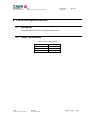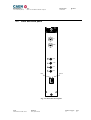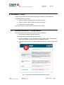
1
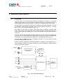
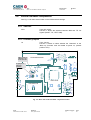
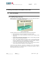
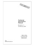
Technical Information Manual Revision n. 5 30 January 2009 MOD. N957 8K MULTICHANNEL ANALYZER NPO: 00105/04:N957x.MUTx/05 CAEN will repair or replace any product within the guarantee period if the Guarantor declares that the product is defective due to workmanship or materials and has not been caused by mishandling, negligence on behalf of the User, accident or any abnormal conditions or operations. CAEN declines all responsibility for damages or injuries caused by an improper use of the Modules due to negligence on behalf of the User. It is strongly recommended to read thoroughly the CAEN User's Manual before any kind of operation. CAEN reserves the right to change partially or entirely the contents of this Manual at any time and without giving any notice. Disposal of the Product The product must never be dumped in the Municipal Waste. Please check your local regulations for disposal of electronics products. Document type: User's Manual (MUT) Title: Mod. N957 8k Multi-Channel Analyzer Revision date: 30/01/2009 Revision: 5 TABLE OF CONTENTS 1. GENERAL DESCRIPTION.........................................................................................................................6 1.1 2. OVERVIEW ...............................................................................................................................................6 TECHNICAL SPECIFICATIONS..............................................................................................................7 2.1 PACKAGING ..............................................................................................................................................7 2.2 POWER REQUIREMENTS ............................................................................................................................7 2.3 FRONT AND BACK PANEL ..........................................................................................................................8 2.4 INPUT/OUTPUT CONNECTIONS ..................................................................................................................9 2.5 FRONT PANEL DISPLAYS ...........................................................................................................................9 2.6 INTERNAL HARDWARE COMPONENTS .....................................................................................................10 2.6.1 Switches .........................................................................................................................................10 2.6.2 Firmware jumpers .........................................................................................................................10 2.7 TECHNICAL SPECIFICATION TABLE .........................................................................................................11 2.8 ANALOG TO DIGITAL CONVERSION .........................................................................................................11 2.8.1 Analog to digital conversion timing ..............................................................................................12 2.8.2 Pile Up Rejection...........................................................................................................................14 2.9 DATA READOUT......................................................................................................................................15 2.10 SCALER AND TIMERS ..............................................................................................................................16 2.10.1 Scaler description..........................................................................................................................16 2.10.2 Timers description .........................................................................................................................16 2.11 FIRMWARE UPGRADE ..............................................................................................................................18 2.11.1 3. N957Upgrade command parameters ............................................................................................18 SOFTWARE INTERFACE........................................................................................................................20 3.1 REGISTER MAP........................................................................................................................................20 3.2 STATUS REGISTER (0X00, R) ...................................................................................................................21 3.3 CONTROL REGISTER (0X01, R/W)............................................................................................................21 3.4 FIRMWARE REVISION REGISTER (0X02, R) ..............................................................................................22 3.5 FIRMWARE DOWNLOAD REGISTER (0X03, R/W) ......................................................................................22 3.6 FLASH ENABLE REGISTER (0X04, R/W) ...................................................................................................22 3.7 PULSER REGISTER (0X05, R/W) ...............................................................................................................22 3.8 DAC REGISTER (0X06, R/W)...................................................................................................................22 3.9 BLOCK DIMENSION REGISTER (0X07, R/W).............................................................................................22 3.10 POTENTIOMETER CONTROL REGISTER (0X08, R/W) ................................................................................23 NPO: 00105/04:N957x.MUTx/05 Filename: N957_REV5.DOC Number of pages: 33 Page: 3 Document type: User's Manual (MUT) 4. Revision: 5 CALIBRATION SET REGISTER (0X09, W)..................................................................................................23 3.12 CALIBRATION CLEAR REGISTER (0X0A, W) ............................................................................................23 3.13 SCRATCH REGISTER (0X0B, R/W)............................................................................................................23 3.14 BUFFER OCCUPANCY REGISTER (0X0C, R/W) .........................................................................................23 3.15 SCALER LOW REGISTER (0X0D, R) .........................................................................................................23 3.16 SCALER HIGH REGISTER (0X0E, R) .........................................................................................................23 3.17 TIMER LOW REGISTER (0X0F, R/W) ........................................................................................................24 3.18 TIMER HIGH REGISTER (0X10, R)............................................................................................................24 3.19 LIVETIME LOW REGISTER (0X11, R) .......................................................................................................24 3.20 LIVETIME HIGH REGISTER (0X12, R).......................................................................................................24 3.21 SOFTWARE CLEAR REGISTER (0X13, W) .................................................................................................24 3.22 SOFTWARE RESET REGISTER (0X14, W) ..................................................................................................24 SOFTWARE TOOLS .................................................................................................................................25 SOFTWARE INSTALLATION: GETTING STARTED ......................................................................................25 4.1.1 Software installation: Windows.....................................................................................................27 4.1.1.1 Software installation: Sample folder ......................................................................................................... 27 4.1.1.2 Software installation: Doc folder .............................................................................................................. 27 4.1.1.3 Software installation: Upgrade folder ....................................................................................................... 27 4.1.2 Hardware installation ...................................................................................................................28 LIBRARY AND DEMO SOFTWARE OVERVIEW ..............................................................................29 5.1 N957TOOL LIBRARY ..............................................................................................................................29 5.1.1 N957Tool library: Overview .........................................................................................................29 5.1.2 N957Tool library: typical usage ...................................................................................................30 5.2 DEMO SOFTWARE ...................................................................................................................................30 5.2.1 6. Revision date: 30/01/2009 3.11 4.1 5. Title: Mod. N957 8k Multi-Channel Analyzer Demo software: N957Demo ..........................................................................................................30 5.2.1.1 N957Demo: Overview .............................................................................................................................. 30 5.2.1.2 N957Demo: Settings ................................................................................................................................. 30 5.2.1.3 N957Demo: configuration file format....................................................................................................... 31 5.2.1.4 N957Demo: output data format................................................................................................................. 32 WINNER SOFTWARE ..............................................................................................................................33 LIST OF FIGURES FIG. 1.1: MOD. N957 BLOCK DIAGRAM ...............................................................................................................6 NPO: 00105/04:N957x.MUTx/05 Filename: N957_REV5.DOC Number of pages: 33 Page: 4 Document type: User's Manual (MUT) Title: Mod. N957 8k Multi-Channel Analyzer Revision date: 30/01/2009 Revision: 5 FIG. 2.1: MOD. N957 FRONT PANEL .....................................................................................................................8 FIG. 2.2: MOD. N957 PCB BOARDAND COMPONENT LOCATION .........................................................................10 FIG. 2.3: SIGNAL CONVERSION TIMING AUTO GATE MODE (NO PILEUP).............................................................13 FIG. 2.4: SIGNAL CONVERSION TIMING AUTO GATE MODE (TRAILING EDGE PILEUP).........................................13 FIG. 2.5: SIGNAL CONVERSION TIMING EXTERNAL GATE MODE .........................................................................14 FIG. 2.6: PUR TIMING FOR EVENT REJECTION (AUTO GATE MODE) ....................................................................15 FIG. 2.7: MAX DATA RATE VS. DATA BLOCK SIZE SETTING ..............................................................................15 FIG. 2.8: LIVETIME STATUS (CONTROL REGISTER <0> = 1 AND AUTO GATE MODE) ..........................................17 FIG. 2.9: LIVETIME STATUS (CONTROL REGISTER <0> = 1 AND EXTERNAL GATE MODE)...................................18 FIG. 4.1: THE SOFTWARE & DOCUMENTATION PACK INTRODUCTION ................................................................25 FIG. 4.2: THE SOFTWARE & DOCUMENTATION PACK WINDOW ..........................................................................26 FIG. 4.3: INSTALLATION FOLDER STRUCTURE .....................................................................................................27 FIG. 4.4: PROGRAM MENU DEMO ........................................................................................................................27 FIG. 5.1: SOFTWARE LAYERS ..............................................................................................................................29 LIST OF TABLES TABLE 2.1: POWER REQUIREMENTS ......................................................................................................................7 TABLE 2.2: MOD. N957 TECHNICAL FEATURES .................................................................................................11 NPO: 00105/04:N957x.MUTx/05 Filename: N957_REV5.DOC Number of pages: 33 Page: 5 Document type: User's Manual (MUT) Title: Mod. N957 8k Multi-Channel Analyzer Revision date: 30/01/2009 Revision: 5 1. General description 1.1 Overview The Mod. N957 is a 8k Multi-Channel (MCA) with USB port, housed in a 1-unit wide standard NIM module. The multichannel analyzer performs the essential function of collecting the data and producing output, in the form of converted value of input peaks. The input pulses can be those produced by a standard spectroscopy amplifier. They can be Gaussian, semi-Gaussian or square waves, unipolar (positive) or bipolar, in a range from 0 to 10 V, with a rise time greater than 0.1 µs. The trigger can be made “on signal” (Auto Gate mode) or “external” (External Gate mode). In the first case a discriminator, with a settable threshold, enables the conversion. In the second case, an external gate is fed to the module, via front panel GATE In connector. The input channel has one peak amplitude stretcher, the output of which is digitised by a 13 bit fast (0.8 μs) ADC featuring a sliding scale technique, to improve the differential non-linearity. Converted waveforms are stored into a 64 KSamples buffer memory. The unit hosts an USB2.0 port (also compatible with USB 1.1), which permits a simple control and data-acquisition via PC. Software Libraries, available for both Windows and Linux platforms, are described in § 5. Future firmware upgrade is possible via USB; only tools developed by CAEN must be used for the firmware upgrade. ANALOG IN ANALOG FRONT-END (TRACK-HOLD/PULSE STRETCHER) GATE IN CHANNEL CONTROLLER (MAX7032S) CONV PUR BUSY N957 CONTROLLER (ALTERA CYCLONE EP1C6) OUTP USB ACQUISITION MEMORY (SRAM 64Kx16) USB PERIPHERAL CONTROLLER Fig. 1.1: Mod. N957 Block Diagram NPO: 00105/04:N957x.MUTx/05 Filename: N957_REV5.DOC Number of pages: 33 Page: 6 Document type: User's Manual (MUT) Title: Mod. N957 8k Multi-Channel Analyzer Revision date: 30/01/2009 Revision: 5 2. Technical specifications 2.1 Packaging The Model N957 is housed in a single width NIM module. 2.2 Power requirements Table 2.1: Power requirements +12 V -12 V +6 V -6 V NPO: 00105/04:N957x.MUTx/05 Filename: N957_REV5.DOC 220 mA 220 mA 600 mA 50 mA Number of pages: 33 Page: 7 Document type: User's Manual (MUT) 2.3 Title: Mod. N957 8k Multi-Channel Analyzer Revision date: 30/01/2009 Revision: 5 Front and back panel Mod. N957 8K MCA IN GATE BUSY CONV PUR OUTP TX/RX LINK ON LINK Fig. 2.1: Mod. N957 Front panel NPO: 00105/04:N957x.MUTx/05 Filename: N957_REV5.DOC Number of pages: 33 Page: 8 Document type: User's Manual (MUT) 2.4 2.5 Title: Mod. N957 8k Multi-Channel Analyzer Revision date: 30/01/2009 Revision: 5 Input/Output connections IN: Type: Input Function: Unipolar (positive) or bipolar in a range from 0 to +10 V, with a rise time greater than 0.1 µs, high impedance. BNC connector (to be connected to Amplifier Analog output); negative inputs are neglected. GATE: Type: Input Function: Temporal window for peak detection (in External Gate mode); Signal must occur prior to and must extend for at least 0.2-μs after the peak; NIM/TTL (automatically recognised) signal, high impedance. BNC connector. BUSY: Type: Output Function: Provides NIM/TTL (switch selected, see § 2.6.1) standard logic level signal to indicate a conversion;. Rise Time ≤ 3.5 ns. Fall Time ≤ 3.5 ns. LEMO connector. CONV: Type: Input Function: Accepts NIM/TTL (switch selected, see § 2.6.1) signal; it is an external conversion inhibit (active high), actually it disables the on going conversions. Input impedance: 50 Ohm; LEMO connector. PUR: Type: Input Function: Pile-up rejection input; accepts NIM/TTL (switch selected, see § 2.6.1) signal; signal must occur before the ADC Conversion (see § 2.8.2). Input impedance: 50 Ohm; LEMO connector (to be connected to Amplifier INHIBIT Output1). OUTP: Type: Output Function: Provides NIM/TTL (switch selected, see § 2.6.1) standard logic level signal programmable via USB. (OUTP default signal: BUFFER_FULL → data loss; it can be turned off by resetting the Full status flag, see § 3.3). LINK: B type USB connector; USB 2.0 compliant Front panel displays BUSY: red LED; light up during the ADC conversion PUR, OUTP: green LEDs (1 per connector); light up as the relevant signal is active CONV: green LED; light up if CONVERSION ENABLE bit (see § 3.3) is ON and CONV input signal is not active. LINK ON: green LED; lights up as USB port is powered TX/RX: yellow LED; signals activity on USB port 1 Amplifier INHIBIT Output provides a logic pulse when the internal pile-up rejection logic detects a distortion of the input signal due to pile-up. NPO: 00105/04:N957x.MUTx/05 Filename: N957_REV5.DOC Number of pages: 33 Page: 9 Document type: User's Manual (MUT) 2.6 Title: Mod. N957 8k Multi-Channel Analyzer Revision date: 30/01/2009 Revision: 5 Internal hardware components See Fig. 2.2 for their exact location on the PCB and their settings. 2.6.1 Switches SW1 Type: DIP switch. Function: it allows the selection between NIM and TTL I/O signals (RIGHT: TTL; LEFT: NIM). 2.6.2 Firmware jumpers J6 SW1 switch for NIM/TTL logic level selection Type: Jumper. Function: it allows to select whether the “Standard” or the “Back up” firmware must be loaded at power on; (default position: STD). DAUGHTER BOARD J6 jumper for firmware selection N957 FPGA USB SECTION Fig. 2.2: Mod. N957 PCB boardand component location NPO: 00105/04:N957x.MUTx/05 Filename: N957_REV5.DOC Number of pages: 33 Page: 10 Document type: User's Manual (MUT) 2.7 Title: Mod. N957 8k Multi-Channel Analyzer Revision date: 30/01/2009 Revision: 5 Technical specification table Table 2.2: Mod. N957 Technical Features 1 No. of ADC channels Unipolar (positive) or bipolar, 300 mV ÷ 10 V range, rise time> 0.1 µs Input signals 13 bit (8192 channels - 8064 valid if sliding scale enabled see 2.8) Resolution ADC Conversion time 0.8 µs Dead Time 4.8 µs LSB 1.22 mV Gate Signal must occur prior to and must extend for at least 0.2-μs after the peak (in External Gate mode); 30 Mbyte/s (USB2.0); 75 Kbytes/s (USB1.1) Maximum transfer rate < 1% from 5% to 95% of input FSR (500 mV ÷ 9.5 V) Differential Non-Linearity < 0.065% from 5% to 95% of input FSR (500 mV ÷ 9.5 V) Integral Non-Linearity <+150 ppm/°C Gain Instability: 2.8 USB port Compatible with USB 1.1 and USB 2.0 30Mbyte/s (USB 2.0 Bulk Transaction Protocol) 3m maximum cable length (longer distance can be achieved with commercial off-the-shelf products) I/O signals NIM/TTL; selected via internal switch SW1 on PCB (see Fig. 2.2) Discriminator Threshold Software programmable, 0 mV ÷ 500 mV range, 100 steps Analog to digital conversion The input stage of the module is basically a linear stretcher which detects the input peak value, while the gate is active, and keeps such value until the end of conversion. Conversion can be triggered automatically (Auto Gate mode) or externally (External Gate mode), depending on Control register setting (see § 3.3). In the first case a discriminator, with a threshold settable via N957_SetLLD function, enables the conversion, which is active as long as the input signal is above such threshold. In the second case, an external gate is fed to the module, via front panel Gate In connector. The output of the peak section is converted by a 13 bit Fast ADC. The ADC section supports the sliding scale technique to reduce the differential non-linearity consists in adding a known value to the analog level to be converted, thus spanning different ADC conversion regions with the same analog value. The known level is then digitally subtracted after the conversion and the final value is sent to the threshold comparator. If the sliding scale is enabled, it reduces slightly the dynamic range of the ADC: the 13-bit digital output is valid from 0 to 8063, while the values from 8064 to 8191 are not correct. NPO: 00105/04:N957x.MUTx/05 Filename: N957_REV5.DOC Number of pages: 33 Page: 11 Document type: User's Manual (MUT) Title: Mod. N957 8k Multi-Channel Analyzer Revision date: 30/01/2009 Revision: 5 2.8.1 Analog to digital conversion timing The signal conversion timing is shown in the following figures (Fig. 2.3, Fig. 2.4, Fig. 2.5 ); the diagram includes five different logic states: • Idle • Track (acquiring data phase) • Settling (Settling time before ADC conversion) • Digitisation (ADC Conversion) • Clear (fast capacitor discharge in the peak section) Idle state: • Auto Gate mode: the input signal after threshold starts the Track (acquiring data) phase • External Gate mode: the occurrence of a GATE pulse starts the Track (acquiring data) phase Track (acquiring data ) state • Auto Gate mode: in the Track state the PEAK output increases according to the input signal. When the first peak is detected starts the Settling phase (where the peak value is held by means of a capacitor) • External Gate mode: in the Track state the PEAK output increases according to the input signal until the highest peak within the GATE ON is reached. When the GATE signal become inactive starts the Settling phase (where the peak value is held by means of a capacitor) Settling (Settling time before ADC conversion) The peak value is held by means of a capacitor until the end of the digital conversion (digitisation) The Settling state takes about 2 µs (settling time) Digitisation state During this phase the output of the PEAK section is converted by a 13 bit Fast ADC (the phase takes 0.8 μsec ) Clear state After the digital conversion, the clear phase takes place by a fast capacitor discharge (about 2 µs) which makes the conversion logic idle again. NPO: 00105/04:N957x.MUTx/05 Filename: N957_REV5.DOC Number of pages: 33 Page: 12 Document type: User's Manual (MUT) Title: Mod. N957 8k Multi-Channel Analyzer Revision date: 30/01/2009 Revision: 5 Threshold Input Peak detection Auto-Gate (Internal) PEAK section Output BUSY Output Conversion Logic State idle track settling digitisa tion clear 2μs 0.8μs 2μs idle Fig. 2.3: Signal conversion timing Auto Gate mode (No Pileup) Threshold Input Peak detection (first peak over threshold) Auto-Gate (Internal) PEAK section Output Busy Output Conversion Logic State idle track settling digitisa tion clear 2μs 0.8μs 2μs idle Fig. 2.4: Signal conversion timing Auto Gate mode (Trailing Edge Pileup) NPO: 00105/04:N957x.MUTx/05 Filename: N957_REV5.DOC Number of pages: 33 Page: 13 Document type: User's Manual (MUT) Title: Mod. N957 8k Multi-Channel Analyzer Revision date: 30/01/2009 Revision: 5 INPUT Peak detection (absolute peak over threshold) GATE PEAK section Output BUSY Output Conversion Logic idle State track settling digitisa tion clear 2μs 0.8μs 2μs idle Fig. 2.5: Signal conversion timing External Gate mode 2.8.2 Pile Up Rejection The PUR input signal prevents the ADC to store piled up events. It accepts NIM/TTL (switch selected, see § 2.6.1) signal. To reject an event, the PUR signal must occur before the conversion logic state Digitisation (before start of BUSY pulse) and must overlap the BUSY output signal (see Fig. 2.6). Threshold Input Peak detection (first peak over threshold) Auto-Gate (Internal) PEAK section Output Busy Output Conversion Logic State PUR NPO: 00105/04:N957x.MUTx/05 Filename: N957_REV5.DOC idle track settling digitisa tion clear idle event Rejected Number of pages: 33 Page: 14 Document type: User's Manual (MUT) Title: Mod. N957 8k Multi-Channel Analyzer Revision date: 30/01/2009 Revision: 5 Fig. 2.6: PUR timing for event rejection (Auto Gate mode) 2.9 Data readout Converted peaks are stored into a 64 KSamples buffer memory, available for data readout via built-in USB2.0 interface (also compatible with USB1.1). Data rate depends, besides the connected PC capabilities, on the board setting via N957_ReadData function, which allows to read a data block of programmable size; the larger the block size, the faster the transfer rate. The average transfer rate of the system can be evaluated in the following way: − Enable software conversion via N957_SetSwConvFlag function − Set the ADC sampling rate via N957_SetADCRate function − Readout data via N957_ReadData function − Acknowledge buffer occupancy via N957_GetBufferOccupancy function During this procedure, the OUTP LED (in default setting) must not light up to signal that buffer memory is full. Max Data Rate (KS/s) with USB2.0 N957_ReadData function always returns the number of readout data; converted waveforms are provided in the form of raw data, which have to be processed by the User’s software tools. 1400 1200 1000 800 600 400 200 0 0 5000 10000 15000 20000 25000 30000 35000 Data Block size (Samples) read_data parameter of N957_ReadData() Fig. 2.7: Max Data Rate Vs. Data Block Size setting NPO: 00105/04:N957x.MUTx/05 Filename: N957_REV5.DOC Number of pages: 33 Page: 15 Document type: User's Manual (MUT) Title: Mod. N957 8k Multi-Channel Analyzer Revision date: 30/01/2009 Revision: 5 2.10 Scaler and Timers The board houses one 32 bit scaler and two 32 bit timers (named Timer and Livetime). 2.10.1 Scaler description Scaler counts the ADC conversion. The Scaler is controlled by the bit 0 of the Control Register: - Control Register <0> = 0: Scaler status: stop - Control Register <0> = 1: Scaler status: count The Scaler is cleared by the following operation: - Dummy write access Software Clear register - Dummy write access Software Reset register Scaler read operation description: 1. Dummy write access Timer Low register: this operation freeze the value of Scaler L/H registers 2. Read the Scaler Low register: Scaler<15..0> 3. Read the Scaler High register: Scaler<31..16> 2.10.2 Timers description Timer and Livetime input clock: 1 KHz Timer is controlled by the bit 0 of the Control Register: - Control Register <0> = 0: Timer status: stop - Control Register <0> = 1: Timer status: count Livetime is controlled by the bit 0 and 6 of the Control Register: - Control Register <0> = 0: Livetime status: stop - Control Register <0> = 1: Livetime status: enabled count NPO: 00105/04:N957x.MUTx/05 in Auto Gate mode (see Fig. 2.8): - Idle and Track status: count (if board is not full) - Settling, Digitisation and Clear status: stop in External Gate mode (see Fig. 2.9): - Track and Settling status: count (if board is not full) - Idle, Digitisation and Clear status: stop Filename: N957_REV5.DOC Number of pages: 33 Page: 16 Document type: User's Manual (MUT) Title: Mod. N957 8k Multi-Channel Analyzer Revision date: 30/01/2009 Revision: 5 Threshold Input Peak detection Auto-Gate (Internal) PEAK section Output BUSY Output Conversion Logic State idle Livetime status track COUNT settling digitisa tion clear idle STOP COUNT COUNT Fig. 2.8: Livetime status (Control Register <0> = 1 and Auto Gate mode) INPUT Peak detection (absolute peak over threshold) GATE PEAK section Output BUSY Output Conversion Logic idle State Livetime status NPO: 00105/04:N957x.MUTx/05 track STOP COUNT Filename: N957_REV5.DOC settling digitisa tion clear idle STOP Number of pages: 33 Page: 17 Document type: User's Manual (MUT) Title: Mod. N957 8k Multi-Channel Analyzer Revision date: 30/01/2009 Revision: 5 Fig. 2.9: Livetime status (Control Register <0> = 1 and External Gate mode) Timer and Livetime are cleared by the following operation: - Dummy write access Software Clear register - Dummy write access Software Reset register Timer and Livetime read operation description: 1. Dummy write access Timer Low register: this operation freeze the value of Timer and Livetime L/H registers 2. Read the Timer Low register: Timer<15..0> 3. Read the Timer High register: Timer<31..16> 4. Read the Livetime Low register: Livetime <15..0> 5. Read the Livetime High register: Livetime <31..16> 2.11 Firmware upgrade The board can store two firmware versions, called STD and BKP respectively; at Power On, a microcontroller reads the Flash Memory and programs the module with the firmware version selected via the J6 jumper (see § 2.6.2), which can be placed either on the STD position, or in the BKP position. It is possible to upgrade the board firmware via USB, by writing the Flash: for this purpose, download the software package available at: http://www.caen.it/nuclear/product.php?mod=N957. The package includes the new firmware release file: N957CTL_revXY.rbf For upgrading the firmware, utilize the upgrade program situated in the folder described in paragraph in § 4.1.1.3; open a DOS Shell, then launch: N957Upgrade -Ifilename (filename= upgrade input file). N.B.: it is strongly suggested to upgrade ONLY one of the stored firmware revisions (generally the STD one): if both revision are simultaneously updated, and a failure occurs, it will not be possible to upload the firmware via VME again! 2.11.1 N957Upgrade command parameters N957Upgrade can be configured via command line through a set of parameters, described in the following. The parameters format is as follows: -param_id[param_value] where: NPO: 00105/04:N957x.MUTx/05 • param_id: a character which identifies the parameter. • param_value: value of the parameter, if foreseen by the parameter itself. Filename: N957_REV5.DOC Number of pages: 33 Page: 18 Document type: User's Manual (MUT) Title: Mod. N957 8k Multi-Channel Analyzer Revision date: 30/01/2009 Revision: 5 Notes about the parameters usage: • If one parameter is not assigned, default value is assumed. • The presentation order of the parameter is arbitrary: • Each not recognised parameter is ignored • Each parameter must be separated from the others via one or more spaces. List of available parameters with relevant default value and usage example: params_list: • -ifilename | -Ifilename filename= upgrade input file. If not specified 'N957.rbf' will be assumed. example: N957Upgrade -i"N957_new.rbf" N957Upgrade -Iupgrade.dat • -s | -S upgrade standard flash page. Default flash page value is 'standard'. example: • -b | -B upgrade backup flash page. Default flash page value is 'standard'. example: • N957Upgrade -b -h | -H show the help screen example: NPO: 00105/04:N957x.MUTx/05 N957Upgrade -s N957Upgrade -h Filename: N957_REV5.DOC Number of pages: 33 Page: 19 Document type: User's Manual (MUT) Title: Mod. N957 8k Multi-Channel Analyzer Revision date: 30/01/2009 Revision: 5 3. Software interface The module can be operated via a set of software accessible registers, whose description is reported in the subsequent sections. 3.1 Register map NPO: 00105/04:N957x.MUTx/05 REGISTER NAME ADDRESS MODE FUNCTION STATUS 0x00 R Status register CONTROL 0x01 R/W Control register FWREV 0x02 R FPGA firmware revision FWDWLND 0x03 R/W R/W configuration rom data FLENA 0x04 R/W Flash enable PULSER 0x05 R/W SW pulse duration DAC 0x06 R/W DAC value setting BLDIM 0x07 R/W Data transfer block size POTCTRL 0x08 R/W Digital pot control register CAL_SET 0x09 W Digital pot bit set register CAL_CLEAR 0x0A W Digital pot bit clear register SCRATCH 0x0B R/W Scratch BUFFER OCCUPANCY 0x0C R Buffer occupancy SCALER_L 0x0D R Scaler (16 LSB) SCALER_H 0x0E R Scaler (16 MSB) TIMER_L 0x0F R/W Timer (16 LSB) TIMER_H 0x10 R Timer (16 MSB) LIVETIME_L 0x11 R Live Timer (16 LSB) LIVETIME_H 0x12 R Live Timer (16 MSB) SW CLEAR 0x13 W Software Clear SW RESET 0x134 W Software Reset Filename: N957_REV5.DOC Number of pages: 33 Page: 20 Document type: User's Manual (MUT) 3.2 3.3 Title: Mod. N957 8k Multi-Channel Analyzer Revision date: 30/01/2009 Revision: 5 Status register (0x00, r) Bit Name Function 3 FLASH BUSY FLAG 0 = Flash ready 1 = Flash busy 2 MEMORY FULL 0 = Data Memory is not full 1 = Data Memory has been filled (can be reset via SWR_RESET or FLAG CLEAR bit of CONTROL REGISTER) 1 MEMORY EMPTY 0 = Data Memory is not Empty 1 = Data Memory is Empty 0 USB TYPE 0 = Full Speed (USB 1.1) 1 = High Speed (USB 2.0) Control register (0x01, r/w) Bit Name Function Default Value 15 OUTP LEMO LOGIC sets the OUTP logic level when OUTP MODE is "PROGRAMMABLE LEVEL" 0 OUTP LEMO MODE selects the signal to present on OUTP front panel connector 00 CONFIG 00 = MEMORY FULL (active high); default LEVEL 13,14 01 = PEAK DETECT (active high when stretcher detects one peak) 10 = PROGRAMMABLE LEVEL (Logic level set by OUTP LEMO LOGIC LEVEL bit) 11 = PULSE MODE (Programmable width active high pulse when PULSER register is written) 12 11 SLIDING SCALE selects sliding scale type: MODE SELECT 0 = Random mode (default) 1 = RAMP mode 0 DAC TEST MODE 0 = DAC test mode disabled ENABLE 1 = DAC test mode enabled. Sliding scale disabled and and the sliding scale 0 DAC is set with the DAC register value (see 0) – only for test purpose 10 RESERVED 9 ACQUISITION 0 = External Gate mode 1 = Auto Gate mode (on discriminator threshold) 1 0 = PUR input sensing disabled 1:= PUR input sensing enabled 1 0 MODE 8 PUR INPUT ENABLE 7 6 SOFTWARE 0 = Software conversion mode disabled CONVERSION 1 = Software conversion mode enabled (the control FPGA auto generates MODE ENABLE conversion requests at a fixed periodic rate – only for test purpose) CONVERSION enables ADC data storage into memory buffer for readout ENABLE 0 = ADC data storage disabled 1 = ADC data storage enabled 0 5 FLAG CLEAR 0= Rearms Memory Full Flag 1= Forces Memory Full Flag Clear (see § 3.2) 0 4 SLIDING SCALE 0 = Sliding Scale disabled 1 = Sliding Scale enabled 1 ENABLE 3..1 0 ADC SWR RATE Selects ADC Conversion Rate when ADC Software Conversion is enabled Timers/scaler enable 0 = 600 S/s 1 = 70 KS/s 2 = 140 KS/s 3 = 250 KS/s 4 = 420 KS/s 5 = 635 KS/s 6 = 850 KS/s 7 = 1 MS/s 0 = Scaler/Timers disabled 1 = Scaler/Timers enabled 7 0 FLAG NPO: 00105/04:N957x.MUTx/05 Filename: N957_REV5.DOC Number of pages: 33 Page: 21 Document type: User's Manual (MUT) 3.4 Revision date: 30/01/2009 Revision: 5 Firmware revision register (0x02, r) Bit 3.5 Title: Mod. N957 8k Multi-Channel Analyzer Name Function 15..8 x FPGA firmware revision (x.y) 7..0 y FPGA firmware revision (x.y) Firmware download register (0x03, r/w) Bit Name Function 15..0 FLDATA Allows to read/write words from/to the on-board flash memory. Must be accessed only through software library API calls. Register default value = 0x0000. 3.6 Flash Enable register (0x04, r/w) Bit Name Function 0 FLENA Allows to enable the flash access for read/write operation. Should be accessed only through software library API calls Register default value = 0. 3.7 Pulser register (0x05, r/w) Bit Name Function 15..0 Pulse width A write access to this register enables a PULSER signal on the board whose duration is equal to the value written. (1.6 µs * register value) Register default value = 0x0000. 3.8 DAC register (0x06, r/w) Bit Name Function 15..0 DAC value Sets DAC value when module is in DAC TEST MODE (see § 3.3) Register default value = 0x0000. 3.9 Block Dimension register (0x07, r/w) Bit Name Function 15..0 BLDIM Dimension of the next data block to read; write to BLDIM the number of samples that the User want to convert/read (through the USB port) Register default value = 0x0020. NPO: 00105/04:N957x.MUTx/05 Filename: N957_REV5.DOC (64 byte packet) Number of pages: 33 Page: 22 Document type: User's Manual (MUT) Title: Mod. N957 8k Multi-Channel Analyzer Revision date: 30/01/2009 Revision: 5 3.10 Potentiometer Control register (0x08, r/w) Bit Name Function 7..0 POTCTRL On board digital trimmer control register. Must be accessed only through software library API calls. Register default value = 0x03. 3.11 Calibration Set register (0x09, w) Bit 15..0 Name Function CAL SET bit X : if 1, sets corresponding bit in Potentiometer Control register. Must be accessed only through software library API calls. 3.12 Calibration Clear register (0x0A, w) Bit Name Function 15..0 CAL CLEAR bit X : if 1, clears corresponding bit in Potentiometer Control register. Must be accessed only through software library API calls. 3.13 Scratch register (0x0B, r/w) Bit Name Function 15..0 Scratch Scratch register for test read/write accesses Register default value = 0xAAAA.. 3.14 Buffer Occupancy register (0x0C, r/w) Bit Name Function 15..0 BUF_OCC Occupancy level of the samples buffer (0-65535) 3.15 Scaler Low register (0x0D, r) Bit Name Function 15..0 SCALER_L Counter (bits 15..0) of performed conversions; enabled via Timers/scaler enable FLAG (see § 3.3) 3.16 Scaler High register (0x0E, r) Bit Name Function 15..0 SCALER_H Counter (bits 31..16) of performed convertions; enabled via Timers/scaler enable FLAG (see § 3.3) NPO: 00105/04:N957x.MUTx/05 Filename: N957_REV5.DOC Number of pages: 33 Page: 23 Document type: User's Manual (MUT) Title: Mod. N957 8k Multi-Channel Analyzer Revision date: 30/01/2009 Revision: 5 3.17 Timer Low register (0x0F, r/w) Bit Name Function 15..0 TIMER_L Acquisition Real Time(bits 15..0); LSB=1ms. Enabled via Timers/scaler enable FLAG (see § 3.3). A write access to this register allows to freeze the values of Scaler L/H, Timer and Livetime L/H registers. 3.18 Timer High register (0x10, r) Bit Name Function 15..0 TIMER _H Acquisition Real Time (bits 31..16); LSB=1ms; enabled via Timers/scaler enable FLAG (see § 3.3). 3.19 Livetime Low register (0x11, r) Bit 15..0 Name Function LIVETIME _L Acquisition Live Time (bits 15..0) ; LSB=1ms; enabled via Timers/scaler enable FLAG (see § 3.3). Auto Gate mode: counts only if board is not full and Conversion logic state is Idle or Track. External Gate mode: counts only if board is not full and Conversion logic state is Track or Settling. 3.20 Livetime High register (0x12, r) Bit Name Function 15..0 Acquisition Live Time (bits 31..16) ; LSB=1ms; enabled via Timers/scaler enable FLAG (see § 3.3). Auto Gate mode: counts only if board is not full and Conversion logic state LIVETIME _H is Idle or Track. External Gate mode: counts only if board is not full and Conversion logic state is Track or Settling. 3.21 Software Clear register (0x13, w) Bit Name Function 15..0 SW CLEAR Any value written to this register generates a software clear which erases the buffer, timers and scalers 3.22 Software Reset register (0x14, w) Bit Name Function 15..0 SW RESET Any value written to this register generates a software reset which erases the buffer, timers and scalers; moreover it resets the FLAG CLEAR and reset Control FPGA state, see § 3.3 NPO: 00105/04:N957x.MUTx/05 Filename: N957_REV5.DOC Number of pages: 33 Page: 24 Document type: User's Manual (MUT) Title: Mod. N957 8k Multi-Channel Analyzer Revision date: 30/01/2009 Revision: 5 4. Software Tools This section describes the CAEN Software package available at CAEN WEB site. The software package provides: • A library for board configuration and raw data acquisition. • A demo program to demonstrate the usage of the library. • A program for firmware update The Library section provides also the USB driver for the board. 4.1 Software installation: Getting started The following instructions will help through the module installation; 1. Download the software package available at: http://www.caen.it/nuclear/product.php?mod=N957 2. Unzip the package on your computer; this will create a folder called N957LibRevXX (XX =release number) and several subfolders with files. 3. Open the index.html file in the N957Lib-RevXX folder, the following window will open: Fig. 4.1: The Software & Documentation Pack introduction NPO: 00105/04:N957x.MUTx/05 Filename: N957_REV5.DOC Number of pages: 33 Page: 25 Document type: User's Manual (MUT) Title: Mod. N957 8k Multi-Channel Analyzer Revision date: 30/01/2009 Revision: 5 If you Click on “Install N957Tool library & N957Demo” the following window will open: Fig. 4.2: The Software & Documentation Pack window The new window allows the following operation: To access the source documentation of the N957 Tool library To access the demo sources files To install the provided software library and the demo application (for Windows) To access all the components of Library and demo for the Linux Operating System To access the WINNER software datasheets NPO: 00105/04:N957x.MUTx/05 Filename: N957_REV5.DOC Number of pages: 33 Page: 26 Document type: User's Manual (MUT) Title: Mod. N957 8k Multi-Channel Analyzer Revision date: 30/01/2009 Revision: 5 4.1.1 Software installation: Windows As installation is completed the structure of the created folders will be as follows: Fig. 4.3: Installation folder structure 4.1.1.1 Software installation: Sample folder This folder provides demo application of the library: N957Demo • Demo: provides the sources of the N957Demo application; it provides the compiled library file (.lib) of N957Tool library and the Visual C++ project file (.vcproj) of N957Demo. • include: provides all the functions necessary to the operation and recompiling of the N957Demo application • Release: provides the sources of the N957Demo application 4.1.1.2 Software installation: Doc folder The Doc folder provides miscellaneous documentation on the N957Tool library 4.1.1.3 Software installation: Upgrade folder This folder provides a console application for the firmware upgrade of the N957 module. The structure of the applications menu will be as follows: Fig. 4.4: Program menu demo NPO: 00105/04:N957x.MUTx/05 Filename: N957_REV5.DOC Number of pages: 33 Page: 27 Document type: User's Manual (MUT) Title: Mod. N957 8k Multi-Channel Analyzer Revision date: 30/01/2009 Revision: 5 It is possible to read the release notes, the readme file, the documentation on the N957Tool library and the N957Demo application. A set of LabView8.2 VIs (in the “LabView” folder) also allows the module’s control. 4.1.2 Hardware installation 1. Connect the USB cable’s A-type connector to an available USB port on your PC. 2. Connect the USB cable’s B-type connector to the USB port on your N957 3. Turn ON the NIM crate . 4. Now the N957 is ready for operation. WARNING (for Windows Users only): Device driver for N957 board is automatically installed by the setup procedure. The host PC should automatically load N957 drivers when connecting USB cable to a powered board. Anyway, if driver files (n957.inf, n957.sys) are requested during installation, they can be found into the following directories: n957.inf :C:\Windows\inf n957.sys: C:\Windows\Systems32\drivers In case of any driver installation issue, please contact [email protected] NPO: 00105/04:N957x.MUTx/05 Filename: N957_REV5.DOC Number of pages: 33 Page: 28 Document type: User's Manual (MUT) Title: Mod. N957 8k Multi-Channel Analyzer Revision date: 30/01/2009 Revision: 5 5. Library and Demo Software overview 5.1 N957Tool library 5.1.1 N957Tool library: Overview N957Tool library is a C-language implemented software tool, which allows the Users to develop applications for operating the N957 board. Fig. 5.1: Software layers The library includes a set of functions grouped by purpose and hardware level • Board handling APIs: allow the management of the board handler. • Miscellaneous APIs: include miscellaneous functions (error decoding, library version etc.). • Level 0 APIs: include lower level functions; allow to access directly the board registers, directly via their physical address. • Level 1 APIs: include middle level functions; allow to access specified board functions, regardless the User’s knowledege of the used registers addresses. Furthermore they provide memory flash read/write capabilities. • Level 2 APIs: include higher level functions; allow to execute macro functions, such as data acquisition management, firmware upgrade, etc. A set of files include (N957Lib.h, N957oslib.h, N957types.h) all the APIs prototypes, declarations depending on the operating system, and data type required in order to develop applications based on the library. NPO: 00105/04:N957x.MUTx/05 Filename: N957_REV5.DOC Number of pages: 33 Page: 29 Document type: User's Manual (MUT) Title: Mod. N957 8k Multi-Channel Analyzer Revision date: 30/01/2009 Revision: 5 5.1.2 N957Tool library: typical usage The typical APIs usage is as follows: • Obtain a valid board handle (N957_Init). • Use the library APIs: N957_####_... all the APIs will use as input parameter, the board handle obtained in the previous step • Release the board handle (N957_End). 5.2 Demo software Demo softwares are N957Tool based applications developed for demonstrative purposes. 5.2.1 Demo software: N957Demo 5.2.1.1 N957Demo: Overview N957Demo is a command line application which shows the N957 operation using the APIs displayed by N957Lib. Demo configures the board according to the parameters provided by the configuration files and executes readout cycles from the board itself. The result of readout (acquired measures) may be issued (if enabled by configuration files) on file in text format and hexadecimal representation. The acquired values are displayed in the form of histogram by applying external GnuPlot (rev> = 4.2). Results of executed operations are displayed on video (wtih either ok or specific error message). A special setting allows the board to produce samples for test and debug purposes. 5.2.1.2 N957Demo: Settings N957Demo can be configured via command line through a set of parameters, described in the following. The parameters format is as follows: -param_id[param_value] where: • param_id: a character which identifies the parameter. • param_value: value of the parameter, if foreseen by the parameter itself. Notes about the parameters usage: NPO: 00105/04:N957x.MUTx/05 • If one parameter is not assigned, default value is assumed. • The presentation order of the parameter is arbitrary: • Each not recognised parameter is ignored Filename: N957_REV5.DOC Number of pages: 33 Page: 30 Document type: User's Manual (MUT) Title: Mod. N957 8k Multi-Channel Analyzer Revision date: 30/01/2009 Revision: 5 • Each parameter must be separated from the others via one or more spaces. • The case of the parameters (id and value) is ignored. • Do not type spaces between the parameter id and its value (example: s100 OK, -s 100 WRONG) • If the parameter value includes spaces (example: fiel names), these must be written between quotation marks without spaces after the parameter id (example: f" my config.conf") • When the application is launched with parameter -h, it is displayed in the list of the available parameters. List of available parameters with relevant default value and usage example: f" my config.conf")-ffilename: output filename. If not specified 'N957Demo.conf' will be assumed. example: • N957Demo -f"N957Demo.conf " • N957Demo -FN957Demo.conf -h: shows the help screen. example: N957Demo -h 5.2.1.3 N957Demo: configuration file format The N957Demo configuration file allows setting the significant parameters. The file format is text type, structured in separate lines. For each line, initial spacing characters (spaces, tabs, etc.) are ignored. param_id [param_value] If the first character line is #, the line is considered Commentary and all content is ignored. The valid lines (not comment) are structured as follows. where: param_id: a keyword that specifies the parameter. param_value: the value of the parameter, if provided by the same parameter. param_id and param_value must be separated by at least a tab Below is reported an example of configuration files, from which it is possible to obtain a list of defined parameters, their meaning and default value: # **************************************************************** # N957Demo Configuration File # **************************************************************** # Lines starting with # (first column) are comments # # The board number BOARD_NUM 0 # # path to the executable file of gnuplot GNUPLOT_PATH "." # # Save readout data into the Output File (0=don't save) LOG_TO_FILE 0 NPO: 00105/04:N957x.MUTx/05 Filename: N957_REV5.DOC Number of pages: 33 Page: 31 Document type: User's Manual (MUT) Title: Mod. N957 8k Multi-Channel Analyzer Revision date: 30/01/2009 Revision: 5 # # Readout data Output Filename ( meaningful only for LOG_TO_FILE!= 0) LOG_FILENAME "data.log" # # Maximum number of samples to acquire (-1 means no limit) MAX_NUM_SAMPLES -1 # # Data Block dimension [1..65536] DATA_BLOCK_DIM 32768 # # Debug mode (0= debug disabled) DEBUG 0 # # Acquisition mode: (0= Ext Gate 1= Auto) ACQ_MODE 1 # # Gnu plot refresh rate (msec) GNU_PLOT_REFRESH # # Gnu plot X scale factor GNU_PLOT_X_SCALE 500 0.3 5.2.1.4 N957Demo: output data format This is a text format output file; on each row it provides data readout from the board in hexadecimal format. The file is generated only if the parameter configuration file LOG_TO_FILE is set to 1: the output filename is specified by the configuration file parameter LOG_FILENAME example: ..... 07c8 07c9 07ca 07c9 07c9 ..... NPO: 00105/04:N957x.MUTx/05 Filename: N957_REV5.DOC Number of pages: 33 Page: 32 Document type: User's Manual (MUT) Title: Mod. N957 8k Multi-Channel Analyzer Revision date: 30/01/2009 Revision: 5 6. WINNER Software WINNER is the universal nuclear spectroscopy for up to 32 inputs that provides different analysis engines for Germanium, NAI, Alpha and CZT, all simultaneously available for corresponding detectors and spectra. WINNER controls data acquisition and incorporates analysis, naturally containing the modules for all auxiliary data files necessary for thorough interpretation and research. Through the multi-document based user interface WINNER offers the possibility to show as much as 1024 different spectra as well as an unlimited number of regions of any individual spectrum in multiple windows. Spectra currently in acquisition or loaded from hard disk are shown and can be handled synchronous, while all the auxiliary data files (such as isotope tables) are handled in the same interface plus many can be loaded parallel. WINNER can directly operate the CAEN N957 Multi-Channel Analyzer. NPO: 00105/04:N957x.MUTx/05 Filename: N957_REV5.DOC Number of pages: 33 Page: 33