1
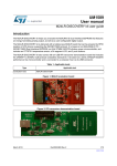
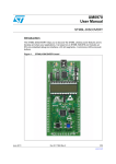
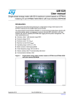
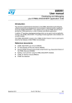
UM1589
User manual
M24LR-Discovery kit user guide
Introduction
The M24LR-Discovery kit helps you evaluate the M24LRXX-E Dual Interface EEPROM that features an
energy harvesting analog output, as well as a user-configurable digital output.
The M24LR-Discovery kit is delivered with a battery-less M24LR board that can be powered by RFID
readers or NFC phones supporting the ISO/IEC15693 protocol. It is based on an M24LR04E-R I²C ISO/IEC15693 Dual Interface EEPROM, an 8-bit STM8L152C6T6 ultralow power microcontroller, and
includes an STTS751 temperature sensor, a 24-segment LCD, and 2 push buttons.
The M24LR-Discovery kit also comes with an USB RF transceiver demonstration board that includes the
CR95HF 13.56-MHz multi-protocol contactless transceiver. It is based on a 32-bit, STM32F103CBT6
performance line microcontroller and is connected to a computer host via its USB connector.
Table 1.
Applicable tools
Type
Evaluation tools
Applicable tool
M24LR-Discovery kit
Figure 1.
M24LR evaluation board
Figure 2.
RF transceiver demonstration board
November 2012
Doc ID 023883 Rev 1
1/15
www.st.com
Contents
UM1589
Contents
1
Quick start . . . . . . . . . . . . . . . . . . . . . . . . . . . . . . . . . . . . . . . . . . . . . . . . . 3
1.1
Getting started with the M24LR04E Dual Interface EEPROM . . . . . . . . . . 3
1.2
Using the M24LR board with Android NFC phones . . . . . . . . . . . . . . . . . . 4
1.3
System requirements . . . . . . . . . . . . . . . . . . . . . . . . . . . . . . . . . . . . . . . . . 4
1.4
Development toolchain . . . . . . . . . . . . . . . . . . . . . . . . . . . . . . . . . . . . . . . . 4
2
Features . . . . . . . . . . . . . . . . . . . . . . . . . . . . . . . . . . . . . . . . . . . . . . . . . . . 5
3
Hardware and layout description . . . . . . . . . . . . . . . . . . . . . . . . . . . . . . . 6
3.1
M24LR board description . . . . . . . . . . . . . . . . . . . . . . . . . . . . . . . . . . . . . . 6
3.2
M24LR board power selection . . . . . . . . . . . . . . . . . . . . . . . . . . . . . . . . . . 7
3.3
RF transceiver board description . . . . . . . . . . . . . . . . . . . . . . . . . . . . . . . . 9
3.4
RF transceiver demonstration board powering and startup . . . . . . . . . . . . 9
3.5
Program/debug the M24LR board . . . . . . . . . . . . . . . . . . . . . . . . . . . . . . 10
3.6
Program/debug the RF transceiver demo board . . . . . . . . . . . . . . . . . . . 10
4
Electrical schematic diagrams . . . . . . . . . . . . . . . . . . . . . . . . . . . . . . . . 11
5
Revision history . . . . . . . . . . . . . . . . . . . . . . . . . . . . . . . . . . . . . . . . . . . 14
2/15
Doc ID 023883 Rev 1
UM1589
1
Quick start
Quick start
The M24LR-Discovery kit is a low-cost and ready-to-use development kit used to evaluate
the functions and performance of the M24LR Dual Interface EEPROM family and its energy
harvesting capability.
For more information on the M24LR-Discovery kit and associated demonstration software,
please visit www.st.com/m24lr04e-discovery.
1.1
Getting started with the M24LR04E Dual Interface EEPROM
1.
On the M24LR board, ensure that a jumper is placed on connector JP1 in the RF power
position (jumper on the right side as shown in Figure 4).
2.
Download and install the M24LR/CR95HF demonstration software available at
www.st.com/m24lr04e-discovery.
3.
Connect the RF transceiver demo board to a PC with a USB cable.
4.
Launch M24LRxx_Application_Software.exe, and select CR95HF Demo Kit. Then,
open the Demo NDEF messages menu and select Show Demo NDEF & Energy
Harvesting.
5.
Place the M24LR board antenna close to the RF transceiver demo board antenna.
6.
The M24LR board starts in Message Display mode (The “M24LR04E-DISCOVERY”
message scrolls across the screen from right to left).
You can read the current NDEF message stored in the M24LR04E-R by clicking the
Read NDEF message button of the PC software.
You can also write an new NDEF message: it will be automatically displayed on the
M24LR board LCD screen after programming.
7.
To change the user mode, press push button B2 (blue button on the left side of the
board). Table 2 lists the user modes available.
Table 2.
Mode
Available user modes
Description
1
Displays the NDEF text message stored in the M24LR04E Dual Interface EEPROM.
2
Displays the voltage powering the M24LR board.
3
Displays the ambient temperature, measured using the temperature sensor.
To study or modify the M24LR board application project related to this demo, please visit
www.st.com/m24lr04e-discovery.
Doc ID 023883 Rev 1
3/15
Quick start
1.2
UM1589
Using the M24LR board with Android NFC phones
1.
Enable NFC communication on your phone (Settings >Wireless and Networks>NFC).
2.
Download the NfcV-Reader Application from Google Play Store.
3.
Launch the NfcV-Reader application.
4.
Place the phone's NFC antenna close to the M24LR board antenna.
The phone powers the M24LR board.
The text message can be changed in the M24LR04E using the NFC phone (select NDEF
function in the NfcV-Reader application and open the Write NDEF message menu).
Please note that performance may vary depending on the NFC phone and its RF
management system.
1.3
1.4
4/15
System requirements
●
Windows® PC (XP or Vista)
●
Two USB cables
Development toolchain
●
Cosmic CXSTM8 compiler
●
STMicroelectronics ST Visual Develop (STVD) integrated development environment
●
STMicroelectronics STLINK/V2 in-circuit debugger and programmer
Doc ID 023883 Rev 1
UM1589
2
Features
Features
The M24LR-Discovery kit includes M24LR board and the RF transceiver board which
offer the following features.
M24LR board
●
M24LR04E-R, a 4-Kbit EEPROM with an I²C-ISO/IEC 15693 dual interface and an
energy harvesting analog output (Vout pin) and a user-configurable digital output (RF
Write-in-progress or Busy pin) in an SO8N package
●
9-turn, 13.56-MHz etched antenna (20mm x 40mm) for RF powering and
communication
●
STM8L152C6T6, 8-bit ultralow power microcontroller with up to 32 Kbytes of Flash
memory, 2 Kbytes of RAM, and 1 Kbyte of Data EEPROM in a 48-pin LQFP package
●
STTS751 I²C low power temperature sensor
●
28-pin LCD on DIP24 socket (24 segments, 4 commons)
●
Two push buttons (User and Reset)
●
HC-49S-C20SSA, a 4-MHz crystal oscillator (not used in demonstration firmware)
●
4-pin connector (CN1) for STM8L programming and debug (SWIM)
●
2-pin connector (CN2) for external power supply source (3 to 6V)
●
5-pin connector (CN3) for M24LR04E-R and I²C bus probing
●
3-pin switch (JP1) to select M24LR board power source (M24LR04E Vout pin or
external)
RF transceiver board
●
CR95HF, a 13.56-MHz multi-protocol contactless transceiver IC with SPI and UART
serial access communication
●
2-turn, 13.56-MHz etched loop antenna (47mm x 34 mm) with associated tuning circuit
and lowpass filter
●
STM32F103CBT6, a 32-bit microcontroller with 128 Kbytes of Flash memory and USB
interface in a 48-pin LQFP package
●
KF33BDT, a 3.3V low dropout (LDO) voltage regulator
●
USB connector
●
NX2520SA, a 27.12-MHz EXS00A-CS01206 crystal oscillator for CR95HF transceiver
●
HC-49XA-C20QQA-8.000MHz for STM32
●
20-pin JTAG connector for STM32 programming and debugging
●
1 push button (Reset)
Doc ID 023883 Rev 1
5/15
Hardware and layout description
UM1589
3
Hardware and layout description
3.1
M24LR board description
Figure 3.
M24LR board layout
24-segment
LCD (U3)
Reset button (B1)
User button (B2)
M24LR board
power selection
connector (JP1)
STM8L152C6T6
microcontroller (U1)
SWIM connector
(CN1)
External
power supply
connector (CN2)
M24LR04E-R
and I²C
connector (CN3)
LDO voltage
regulator for
external power
input (U5)
4-MHz crystal
oscillator (X1)
M24LR04E-R
Dual interface
EEPROM (U4)
STTS751 I²C
temperature
sensor (U2)
9-turn,
13.56-MHz
etched loop
antenna
6/15
Doc ID 023883 Rev 1
UM1589
3.2
Hardware and layout description
M24LR board power selection
When jumper JP1 is set in the “RF power” position (Figure 4), the M24LR board is powered
by the M24LR04E-R energy harvesting analog output (Vout pin). In this configuration, the
M24LR board is powered by the magnetic field flowing into its 9-turn, etched loop antenna,
delivered from a 13.56-MHz RF source, such as an RFID reader or an NFC phone. The DC
voltage supply delivered by the M24LR04E-R Vout pin is filtered by an 10-nF capacitor
(C19) and stored in the 150-µF capacitor (C22). The low dropout (LDO) voltage regulator
(U5) is bypassed, so the M24LR04E-R voltage is filtered but not regulated.
Figure 4.
Jumper JP1 set in RF power position
When jumperJP1 is set in the “REG 3.3" position (Figure 5), the M24LR board is powered by
the external power supply connected on connector CN2. The voltage applied on the external
power supply connector CN2 is regulated by the 3.3V voltage regulator (U5). The external
power supply voltage can be from 3.3 to 6V.
Using an external power supply is necessary when programming or debugging the STM8L
MCU using the SWIM connector (CN1).
Figure 5.
Jumper JP1 in “REG_3V3” position and external power connection
It is also possible to connect an external antenna demonstration board featuring the energy
harvesting function (ANTX-M24LRXXE) to improve or simply evaluate the energy harvesting
function using a different antenna.
Doc ID 023883 Rev 1
7/15
Hardware and layout description
UM1589
Figure 6 and Figure 7 illustrate the use of an external antenna using the ANT1-M24LR16E
demonstration board.
8/15
●
Figure 6 shows a possible direct connection of the Vout voltage coming from the ANT1M24LR16E antenna demo board on jumper JP1 to bypass the voltage regulator (U5).
●
Figure 7 shows the connection of the Vout voltage coming from the ANT1-M24LR16E
antenna demo board on connector CN2 to use the voltage regulator (U5). Jumper JP1
must be set as shown in Figure 5.
Figure 6.
External antenna connection with voltage regulator bypass
Figure 7.
External antenna connection using M24LR board voltage regulator
Doc ID 023883 Rev 1
UM1589
3.3
Hardware and layout description
RF transceiver board description
Figure 8.
RF transceiver board layout (top and bottom)
USB
connector (J1)
LDO regulator
User LED 1
STM32F103CBT6
20-pin JTAG
connector (J3)
27.12-MHz
crystal oscillator
CR95HF RF IC
Reset button
2-turn,13.56-MHz
loop antenna
3.4
RF transceiver demonstration board powering and startup
The RF transceiver demonstration board is powered by the USB bus.
When powered up, the CR95HF starts in an autonomous mode called “tag hunting”: the red
LED 1 lights up every time a tag is recognized. During Tag Hunting mode, the RF
transceiver demonstration board switches ON and OFF the magnetic field at each RF
protocol change. A constant magnetic field is naturally more appropriate to evaluate and
develop battery-less applications based on the Energy Harvesting capability of the
M24LRXXE-R EEPROM Family.
Tag Hunting mode persists until the M24LR/CR95HF demonstration software is launched
and the CR95HF is initialized by the software. At this moment, both Tag Hunting mode and
the RF field stop. To activate a constant magnetic field emission, it possible either to open
the Demo NDEF messages menu and select Show Demo NDEF & Energy Harvesting or
send a single ISO/IEC15693 RF command (Inventory, Read.).
Doc ID 023883 Rev 1
9/15
Hardware and layout description
3.5
UM1589
Program/debug the M24LR board
To program or debug an STM8L microcontroller application on the M24LR board, simply:
1.
Set jumper JP1 in the “REG_3V3” position.
2.
Connect an external power supply to the “3V3-6V” connector (CN2).
3.
Connect the 4-pin SWIM connector of the STLINK/V2 in-circuit debugger and
programmer to connector CN1 as described in Table 3.
Table 3.
3.6
M24LR board programming and debug connector
Pin
CN2
Designation
1
Vcc
VDD supply from M24LR board
2
PA0
SWIM data input/output
3
GND
Ground supply
4
RESET
SWIM reset
Program/debug the RF transceiver demo board
To program or debug an STM32 microcontroller application on the RF transceiver
demonstration board, simply:
1.
Connect the 20-pin JTAG/SWD flat ribbon of the STLINK/V2 in-circuit debugger and
programmer to the RF transceiver demonstration board JTAG connector (J2).
For more information, documentation about the STLINK/V2 in-circuit debugger and
programmer, please visit www.st.com
10/15
Doc ID 023883 Rev 1
CN1
0
R3
C7
1uF[ceramic]
VCC
Not Fitted
VCC
1
2
3
4
LCD_SEG23
LCD_SEG1
LCD_SEG2
LCD_SEG3
LCD_SEG4
LCD_SEG5
LCD_SEG6
LCD_SEG7
LCD_COM3
LCD_SEG8
LCD_SEG9
LCD_SEG10
VCC
VCCA
RESET#
OSC_I N
OSC_OUT
LCD_COM0
LCD_COM1
LCD_COM2
LCD_SEG0
C1
1uF
1
2
3
4
5
6
7
8
9
10
11
12
13
14
15
16
17
18
19
20
21
22
23
24
STM8L 152C6T6
PA0
PA1
PA2
PA3
PA4
PA5
PA6
PA7
AVSS
VDD
VDDA
VREF+
VL CD
PE0
PE1
PE2
PE3
PE4
PE5
PD0
PD1
PD2
PD3
PB0
U1
C4
100nF
VCC
C3
100nF
PE7
PE6
PC7
PC6
PC5
PC4
PC3
PC2
VSSI O
VDDI O
PC1
PC0
PD7
PD6
PD5
PD4
PF0
PB7
PB6
PB5
PB4
PB3
PB2
PB1
BEAD
L1
48
47
46
45
44
43
42
41
40
39
38
37
36
35
34
33
32
31
30
29
28
27
26
25
C2
1uF
U3
GH08172T
RESET
LED
5
4
3
2
1
2
1
3
2
660
R7
C8
100nF
Vout
BYPASS
blue
LD1
RESET#
VCC
B2
USER(Blue)
C21
VCC
[N/A]
C22
C17
1uF[ceramic]
C18
100nF
C15
4.7uF
5
4
User
1
2
3
4
Antenna
VCC
C9
100nF
R1
4K7
VCC
TL NK157M006R2500(150uF)
Z1
MMSZ 5227BT1(do not it)f
LD3985M33R
Vin
INHI BI T
GND
U5
I2C connector
I2C1_SCL
I2C1_SDA
RF_WI P/BUSY
JP1
1
RF_POWER
C16
1uF[ceramic]
REG_3V3
Header 5
CN3
CN2
1
3
2
B1
RESET(Black )
External DC +3V3-6V
I2C1_SCL
I2C1_SDA
LCD_SEG21
LCD_SEG20
LCD_SEG19
LCD_SEG18
RF_WI P/BUSY
LCD_SEG17
LCD_SEG16
LCD_SEG15
LCD_SEG14
LCD_SEG13
LCD_SEG12
LCD_SEG11
VCC
PE7
LED
User_PB
OSC32_OUT
OSC32_
IN
TemSensor_TNT
LCD_SEG23
LCD_SEG22
TP1
VCCA
C5
100nF
2
1
2
1
3
4
3
4
SWIM
LCD_SEG22
28
28
27
1
1
2
LCD_SEG1
LCD_SEG0
2
27
LCD_SEG21
26
LCD_SEG20
25
25
3
26
4
LCD_SEG2
3
LCD_SEG18
LCD_SEG3
4
LCD_SEG19
24
5
LCD_SEG4
5
24
LCD_SEG17
23
6
LCD_SEG5
6
23
LCD_SEG16
22
7
LCD_SEG6
7
22
LCD_SEG15
21
8
LCD_SEG7
20
9
LCD_SEG8
9
21
LCD_SEG13
8
20
LCD_SEG14
19
19
10
LCD_SEG9
18
11
10
LCD_COM0
LCD_SEG10
11
18
LCD_SEG12
17
12
17
LCD_COM1
LCD_SEG11
12
16
COM0
COM3
15
COM1
COM2
14
13
Doc ID 023883 Rev 1
LCD_COM3
1
OSC32_
IN
0
R5
M24L R04E- RMN6T/2
8
7
6
5
VCC
VCC
I2C1_SDA
TemSensor_TNT
I2C1_SCL
RF_WI P/BUSY
I2C1_SCL
I2C1_SDA
R6
20K
C14
10nFVCC
R8 R9 R10
20K 15K 15K
RF_POWER
Vout
VCC
AC0 RF WI P/BUSY
AC1
SCL
VSS
SDA
0
C13 STTS751-0WB3F
100nF
C20
[N/A]
6
5
4
OSC32_OUT
R4
33K U2
1
Addr/Therm SDA
2
GND
EVENT
3
VDD
SCL
C19
10nF R11
U4
60
R2
X1
HC- 49S-C20SSA-4.000
OSC_I N
OSC_OUT
X2
MC306- G-06Q-32.768 (manufacturer JFVNY)
20pF
C10
20pF
C6
Not Fitted
6.8pF
C11
6.8pF
C12
VCC
User_PB
2
3
Figure 9.
4
4
LCD_COM2
UM1589
Electrical schematic diagrams
Electrical schematic diagrams
M24LR board schematics
11/15
Electrical schematic diagrams
UM1589
Figure 10. RF transceiver demonstration board schematics (STM32 connections)
12/15
Doc ID 023883 Rev 1
UM1589
Electrical schematic diagrams
Figure 11. RF transceiver demonstration board schematics (CR95HF connections)
Doc ID 023883 Rev 1
13/15
Revision history
5
UM1589
Revision history
Table 4.
14/15
Document revision history
Date
Revision
06-Nov-2012
1
Changes
Initial release.
Doc ID 023883 Rev 1
UM1589
Please Read Carefully:
Information in this document is provided solely in connection with ST products. STMicroelectronics NV and its subsidiaries (“ST”) reserve the
right to make changes, corrections, modifications or improvements, to this document, and the products and services described herein at any
time, without notice.
All ST products are sold pursuant to ST’s terms and conditions of sale.
Purchasers are solely responsible for the choice, selection and use of the ST products and services described herein, and ST assumes no
liability whatsoever relating to the choice, selection or use of the ST products and services described herein.
No license, express or implied, by estoppel or otherwise, to any intellectual property rights is granted under this document. If any part of this
document refers to any third party products or services it shall not be deemed a license grant by ST for the use of such third party products
or services, or any intellectual property contained therein or considered as a warranty covering the use in any manner whatsoever of such
third party products or services or any intellectual property contained therein.
UNLESS OTHERWISE SET FORTH IN ST’S TERMS AND CONDITIONS OF SALE ST DISCLAIMS ANY EXPRESS OR IMPLIED
WARRANTY WITH RESPECT TO THE USE AND/OR SALE OF ST PRODUCTS INCLUDING WITHOUT LIMITATION IMPLIED
WARRANTIES OF MERCHANTABILITY, FITNESS FOR A PARTICULAR PURPOSE (AND THEIR EQUIVALENTS UNDER THE LAWS
OF ANY JURISDICTION), OR INFRINGEMENT OF ANY PATENT, COPYRIGHT OR OTHER INTELLECTUAL PROPERTY RIGHT.
UNLESS EXPRESSLY APPROVED IN WRITING BY TWO AUTHORIZED ST REPRESENTATIVES, ST PRODUCTS ARE NOT
RECOMMENDED, AUTHORIZED OR WARRANTED FOR USE IN MILITARY, AIR CRAFT, SPACE, LIFE SAVING, OR LIFE SUSTAINING
APPLICATIONS, NOR IN PRODUCTS OR SYSTEMS WHERE FAILURE OR MALFUNCTION MAY RESULT IN PERSONAL INJURY,
DEATH, OR SEVERE PROPERTY OR ENVIRONMENTAL DAMAGE. ST PRODUCTS WHICH ARE NOT SPECIFIED AS "AUTOMOTIVE
GRADE" MAY ONLY BE USED IN AUTOMOTIVE APPLICATIONS AT USER’S OWN RISK.
Resale of ST products with provisions different from the statements and/or technical features set forth in this document shall immediately void
any warranty granted by ST for the ST product or service described herein and shall not create or extend in any manner whatsoever, any
liability of ST.
ST and the ST logo are trademarks or registered trademarks of ST in various countries.
Information in this document supersedes and replaces all information previously supplied.
The ST logo is a registered trademark of STMicroelectronics. All other names are the property of their respective owners.
© 2012 STMicroelectronics - All rights reserved
STMicroelectronics group of companies
Australia - Belgium - Brazil - Canada - China - Czech Republic - Finland - France - Germany - Hong Kong - India - Israel - Italy - Japan Malaysia - Malta - Morocco - Philippines - Singapore - Spain - Sweden - Switzerland - United Kingdom - United States of America
www.st.com
Doc ID 023883 Rev 1
15/15