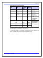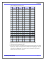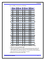
1
ProceV™ Preliminary Data Book January 2014 GiDEL products and their generated products are not designed, intended, authorized, or warranted to be suitable for use in life-support applications, devices or systems or other critical applications. © 1993 - 2014 by GiDEL Ltd. All rights reserved. GiDEL, ProceV™, PSDB, ProcWizard™, ProcMultiPort™ and other product names are trademarks of GiDEL Ltd., which may be registered in some jurisdictions. This information is believed to be accurate and reliable, but GiDEL LTD. assumes no responsibility for any errors that may appear in this document. GiDEL reserves the right to make changes in the product specifications without prior notice. Windows, Stratix V, TMS320C6414, DDRII, CameraLink and other brand and product names are trademarks or registered trademarks of their respective holders. USA 1600 Wyatt Drive Suite 1 Santa Clara CA 95054, USA Tel: 1 - 408 - 969 – 0389 Fax: 1 - 408 - 465 – 7361 Worldwide 2 Ha'ilan Street, P.O. Box 281 Or Akiva, IsraIsrael 30600 Fax: +972 - 4610 - 2501 Tel: +972 - 4610 - 2500 [email protected] Web: www.GiDEL.com [email protected] [email protected] Contents Contents ............................................................................................................................ iii Figures ............................................................................................................................... vi Tables ............................................................................................................................... vii 0.1 Scope..............................................................................................................................1 0.1 Introduction ..................................................................................................................2 3.0 Key Features .................................................................................................................4 3.1. ProceV Performance...................................................................................... 5 4.0 Standard Models ..........................................................................................................6 5.0 Architecture ..................................................................................................................8 5.1. ProceV Block Diagram ................................................................................... 8 5.2. ProceV Signal Buses ................................................................................... 10 5.2.1. PSDB Connector (J4) Buses- Single-Ended Mode .............................. 10 5.2.2. PSDB Connector (J4) Buses- LVDS mode .......................................... 11 5.2.3. Internal Bus ......................................................................................... 12 4.2.5. General purpose I/O Bus ..................................................................... 12 5.3. ProceV Clocking System ............................................................................. 12 5.3.1. ProceV Global Clocks ......................................................................... 13 5.3.2. ProceV Individual Clocks..................................................................... 13 5.3.3. ProceV High-Speed Reference clocks ................................................ 14 6.0 DMA Controller .........................................................................................................15 6.1. DMA Performance ....................................................................................... 16 7.0 Connectors ..................................................................................................................17 7.1. Board Connectors Overview ........................................................................ 17 7.2. CXP Connector (J1) ..................................................................................... 19 7.3. SFP+ Connectors (J18) ............................................................................... 20 7.4. High Speed Inter-Board Connectors (J6,7) .................................................. 21 7.5. PSDB Connector (J4) .................................................................................. 24 7.6. External I/O Connector (J3) ......................................................................... 27 7.7. RJ45 Connector (J8) .................................................................................... 28 7.8. External Power (12V) Connector (J2)........................................................... 29 Preliminary ProceV Data Book iii Table of Contents 8.0 Memories ....................................................................................................................30 8.1. Two-level structure Stratix V embedded memory ......................................... 30 8.2. On-board Memory Blocks - DDRII+ SRAM (optional).................................... 30 8.3. ECC DDR3 DRAM SODIMM Modules – 72 bit wide .................................... 31 8.4. SODIMM Connectivity .................................................................................. 32 8.5. SRAM Connectivity ...................................................................................... 34 9.0 LEDs ...........................................................................................................................36 9.1. Power LEDs ................................................................................................. 36 9.2. Status LEDs ................................................................................................. 36 9.3. General Purpose User LEDs ........................................................................ 37 9.4. SFP+ LEDs .................................................................................................. 37 10.0 Technical Specifications ..........................................................................................38 10.1. Electrical and Mechanical Environment ........................................................ 38 10.1.1. Humidity .............................................................................................. 38 10.1.2. Temperature........................................................................................ 38 10.2. MTBF ........................................................................................................... 38 10.3. ProceV Mechanical Description ................................................................... 39 4..5. Power Consumption..................................................................................... 40 10.5. ProceV Timing Model .................................................................................. 42 10.5.1. Groups Skew....................................................................................... 42 10.5.2. Clock Accuracy ................................................................................... 43 10.5.3. System I/O Frequency......................................................................... 43 11.0 Installation ................................................................................................................44 11.1. Requirements .............................................................................................. 44 44.2. Installing the ProceV board .......................................................................... 44 44.1. Loading Designs in PCI Express Mode ........................................................ 45 12.0 GiDEL Accessories..................................................................................................46 12.1. GiDEL Proc Developer's Kit™ ...................................................................... 46 12.2. GiDEL ProcWizard™ ................................................................................... 46 12.3. GiDEL ProcMultiPort™ ................................................................................ 47 12.4. GiDEL ProcMegaDelay™ ............................................................................ 48 12.5. GiDEL ProcMegaFIFO™ ............................................................................. 48 12.6. GIDEL PSDB Daughterboards ..................................................................... 49 Preliminary ProceV Data Book iv Table of Contents 13.0 Appendix ...................................................................................................................50 13.1. Throughput Calculations .............................................................................. 50 13.1.1. M20K Throughput Calculations ........................................................... 50 13.1.2. Stratix V MLAB Throughput Calculations ............................................. 50 13.1.3. On-board SRAM Memories Throughput Calculations .......................... 50 13.1.4. DDR3 SDRAM SODIMM Throughput Calculations .............................. 51 41.4.4. Additional Devices Needed ................................................................. 51 14.0 References .................................................................................................................52 14.1. References .................................................................................................. 52 15.0 Glossary ....................................................................................................................53 16.0 Revision History .......................................................................................................54 16.1. PCB History ................................................................................................. 54 16.2. Firmware History .......................................................................................... 54 16.3. ProceV Data Book History ........................................................................... 54 Preliminary ProceV Data Book v Figures Figure 1: ProceV System Block Diagram ................................................................................................... 8 Figure 2: ProceV Clock System ................................................................................................................ 12 Figure 3: Components Side (CS) Connectors ........................................................................................... 17 Figure 4: Print Side (PS) Connectors ........................................................................................................ 18 Figure 5: ProceV Mechanical Dimensions (in mm) ................................................................................. 39 Preliminary ProceV Data Book vi Tables Table 1: ProceV Memory Throughput ........................................................................................................ 5 Table 2: GiDEL ProceV Standard Models ................................................................................................. 6 Table 3: DMA Performance Benchmark System ..................................................................................... 16 Table 4: DMA Performance...................................................................................................................... 16 Table 5: Component Side Connector Description .................................................................................... 17 Table 6: Print Side Connector Description ............................................................................................... 18 Table 7: CXP Top-Level Signals .............................................................................................................. 19 Table 8: SFP+ Top-Level Signals ............................................................................................................. 20 Table 9: HS-B Connector (J6) Pin-out...................................................................................................... 21 Table 10: HS-C Connector (J7) Pin-out.................................................................................................... 22 Table 11: HS Connectors’ Top-Level Signals .......................................................................................... 23 Table 12: PSDB_L(J4) connector pin-out ................................................................................................ 25 Table 13: PSDB_L (J4) pin-out in LVDS Mode ...................................................................................... 26 Table 14 : J3-General Purpose IO Connector Assignments ..................................................................... 27 Table 15: IO Working Frequency ............................................................................................................. 27 Table 16: 88E1118R PHY Top-Level Signals......................................................................................... 28 Table 17: Power Connector Pin Map (cable side) .................................................................................... 29 Table 18: Power Connector (J2) Pin-out .................................................................................................. 29 Table 19: SODIMM Top-Level Signals ................................................................................................... 32 Table 20: SRAM Top-Level Signals ........................................................................................................ 34 Table 21: Power LEDs. ............................................................................................................................. 36 Table 22: Status LEDs .............................................................................................................................. 36 Table 23: ProceV Operating Conditions ................................................................................................... 38 Table 24: Maximum current Limits .......................................................................................................... 40 Table 25: ProceV Internal Voltage Sources.............................................................................................. 40 Table 26: Groups Skew ............................................................................................................................. 42 Table 27: Clock Accuracy ........................................................................................................................ 43 Table 28: System I/O Frequency .............................................................................................................. 43 Table 29: PSDB Connector Heights. ........................................................................................................ 51 Table 30: Table of Acronyms ................................................................................................................... 53 Table 31: PCB History .............................................................................................................................. 54 Table 32: Firmware History ...................................................................................................................... 54 Table 33: Data Book History .................................................................................................................... 54 Preliminary ProceV Data Book vii 1.0 Scope The purpose of this data book is to provide architectural, hardware and installation information for the ProceV™ system. This data book is organized in the following chapters: Introduction – Board description and purpose. Key Features – Main features and performance. Standard Models – Standard product models available. Architecture – Board architecture, components, busses and clocks. DMA Controller – DMA operation and performance. Connectors – Board connectors' description and pin-out. Memories – Memory structure. LEDs – LEDs functions. Technical Specifications - Electrical, mechanical and other technical specifications. Installation – Requirements and installation instructions. GIDEL Accessories – GiDEL management software and IPs. Appendix – Additional information. References – List of referenced documents. Glossary – Term definitions and acronyms. Revision History – Board and document revision history. Preliminary ProceV Data Book 1 2.0 Introduction The ProceV™ system provides a high-capacity, high-speed FPGA-based platform along with 16+GB of memory with ~20GB/s sustain access rate. The combination of high-speed direct communication to the FPGA via PCIe gen 3, CXP, SFP+, RJ45 and General Purpose physical layer interface makes the ProceV ideal for HPC(High Performance Computing) and high performance low-latency networking applications. The ProceV architecture, based on Altera's Stratix V FPGA technology, is capable of running at typical system speeds of 150-450 MHz. The ProceV is 8-lane PCI Express hosted offering both high performance and flexible architecture, based on massive memory and diverse add-on daughterboards for large application needs. In addition to two SODIMM sockets, 1.6Gb/s each, providing up to 16 GB of ECC DDR3 memory, the ProceV provides an option for 2×144 Mb or 2×36 Mb on-board DDRII+ SRAM memory. This vast memory conjoined with PCIe connection permits strong co-processing between a PC with standard OS and the FPGA accelerator. The ProceV system, supported by GiDEL's ProcDeveloper's Kit™ management software and soft IPs, offers an incredible improvement in time-to-market. In addition, the ProceV is enhanced by GiDEL’s line of PSDB daughterboards enabling interfacing with external I/O lines and video applications, including SDI, DVI and Camera Link standards. ProceV supports new simple SerDes-based fast connections between boards and accessories of up to 169 Gb/s full duplex. The ProceV system is suitable for the following applications: High-speed low latency networking and network analysis Trading Life science Applications ASIC and SoC Prototyping DSP (Digital Signal Processing) and HPRC (High Performance Reconfigurable Computing) Surveillance, Machine Vision and Imaging High performance acquisition systems Preliminary ProceV Data Book 2 Introduction The ProceV all-inclusive system, composed of on-board controllers and automatic code generation application software, eliminates the need to: Write a PCI Express driver. Write an application driver layer. Define board constraints. Design memory controller. Write environment FPGA code. With the ProceV system and supporting development tools designers can focus on their proprietary value-added design instead of spending valuable time recreating standard design components. GiDEL’s soft IPs and automatic HDL code generation enable high speed and easy-to-use parallel access to large memories. User designs may be in HDL, C-based, Simulink (graphical design) or any combination of them. For information on other design entry tools, please contact GiDEL. Preliminary ProceV Data Book 3 3.0 Key Features Support Altera Stratix V GX (A3, A7, AB) and GS (D5, D8) FPGAs. Gen-3 8-lane PCI Express host interface and stand alone option. Four level memory structure (16+ GB). Up to 2640 M20K (20K-bit) SRAM blocks (50 Mb) - 8,000 GB/s typical throughput Up to 17,960 Enhanced MLAB (640-bit) SRAM blocks (8 Mb) 2 × DDR3 ECC SODIMMs Banks with up to a total of 16 GB at a sustain throughput of 19.2 GB/s Optional 2 × 144Mb or 2 × 36Mb DDRII+ SRAM memories (up to 450Mhz) Typical system frequency of 150 - 450MHz. Up to 32 DMA channels. Up to 3,926 of 18x18 bit multipliers implemented in Stratix V devices. Optional: 1 CXP connector cage suitable for 100 Gigabit Ethernet (100GBASE-CR10, 100GBASE-SR10), 3×40 Gigabit Ethernet, or single Infiniband 12×QDR link Optional: 2 SFP+ cage suitable for 10 Gigabit Ethernet and Optical Transport Network Optional: RJ45 port suitable for 1000MBase-T and 100MBase-TX 2 High-Speed Inter-Board connectors (up to 12×14.1 Gb/s) for board to board and Proc High-Speed (PHS) daughterboards connectivity PHS daughterboards enabling additional protocol and connectivity options such as CoaXPress, QSFP and SAS/SATA. 12 general purpose LVTTL External IOs Support for a single PSDB type 1 daughter board used for a GiDEL’s off-the-shelf or user add-on Interface including logic Analyzer mictors, Camera Link, SDI, DVI and other interfaces. Immediate and simple high bandwidth use of the on-board memories with the innovative GIDEL ProcMultiPort™ configurable IP (a part of GIDEL Proc Developer's Kit). Each memory can be used for parallel data streaming, and for debug data capture. Flexible clocking System. Temperature monitoring. Supported by GiDEL's Proc Developer's Kit management software. Drivers for Windows and Linux 64-bit Operating Systems. Preliminary ProceV Data Book 4 Key Features 3.1. ProceV Performance The ProceV system provides high performance capabilities. Table 1 details the ProceV’s throughput and memory capacity. Note that the performance is dependent on Proc board model. Table 1: ProceV Memory Throughput Memory Structure Capacity Embedded in FPGA Up to 2640 x M20K Blocks 300 MHz 8,000 GB/s Optional On-Board Memory 2 x 144Mb or 2 x 36Mb SRAM (36-bit) 800 Mb/s 6.4 GB/s SODIMM Modules 2 x 8GB DDR3 1600 Mb/s 19.2 GB/s Typical Data Rate Per Single Data Bit Throughput* * Refer to the Appendix for throughput calculations (paragraph 13.1) For further information regarding the embedded memory blocks, refer to the Altera Stratix V Handbook. Preliminary ProceV Data Book 5 4.0 Standard Models This chapter details the standard models product available. The model names have the following structure: Proceaa-bcdeefg, where: aa: Type of Stratix V devices: GX Device: A3, A7, AB GS Device: D8 b: Speed grade: A = -1 speed grade, B = -2 speed grade, C = -3 speed grade c: CXP Option: X=CXP, Blank= without CXP d: SFP+ option: S=with SFP+ A and B, Blank=without SFP+ ee: 1Gbit Ethernet PHY Option: 1G =with PHY, Blank without PHY f: SRAM Option: M = 2×36 Mb 450 Mhz DDRII+ SRAMs, Blank= without SRAM, other combinations are available for a quantity if 10 or more boards g: External Clock Option: CK= External clock, Blank= without external clock The following table is a list of the available ProceV models: Table 2: GiDEL ProceV Standard Models Ordering Code** (Basic Models) Stratix V Device Speed DDR III LEs* Grade SODIMM Sockets M20K Blocks 18×18 Multipliers ProceVA3-C 5SGXA3 -3 2 340 K 957 512 ProceVA3-CX 5SGXA3 -3 2 340 K 957 512 ProceVA3-CS 5SGXA3 -3 2 340 K 957 512 ProceVA3-CXS 5SGXA3 -3 2 340 K 957 512 ProceVA3-B 5SGXA3 -2 2 340 K 957 512 ProceVA3-BX 5SGXA3 -2 2 340 K 957 512 ProceVA3-BS 5SGXA3 -2 2 340 K 957 512 ProceVA3-BXS 5SGXA3 -2 2 340 K 957 512 Preliminary ProceV Data Book 6 Board Architecture (Table 2 – continued from previous page) Ordering Code** (Basic Models) Stratix V Device Speed DDR III LEs* Grade SODIMM Sockets M20K Blocks 18×18 Multipliers ProceVA7-BXS 5SGXA7 -2 2 622 K 2,560 512 ProceVAB-BXSM 5SGXAB -2 2 952K 2,640 704 ProceVD8-BXSM 5SGSD8 -2 2 695 K 2,567 3,926 * LE=Logic Element. For further information on the Stratix V LEs, refer to Stratix V Device Handbook (Altera Corporation). **For other ProceV models, contact GiDEL. NOTE: Default transceivers are K2=12.5 Gb/s; for transceivers K1=14.1 Gb/s, please contact GiDEL. Preliminary ProceV Data Book 7 5.0 Architecture This chapter details the ProceV architecture and components. 5.1. ProceV Block Diagram The ProceV system Block Diagram is shown in Figure 1. BANK B BANK C DDR3 SODIMM 4GB/8GB 1600 MHz (J11) DDR3 SODIMM 4GB/8GB 1600 MHz (J12) 72 External I/Os (J3) 72 12 115* RJ45 (J8) (optional) Stratix V FPGA SFP+ (J18) (optional) SFP+ (J18) (optional) CXP+ (J1) (optional) 8 HS_B Inter-board Connector (J6), 4 HS_C Inter-board Connector (J7), 12 36 36 DDRII SRAM 36 Mb or 144 Mb, 450 MHz (optional) DDRII SRAM 36 Mb or 144 Mb, 450 MHz (optional) BANK E BANK D PCIe x 8 Gen 3 Bridge Power Connector (J2) x8 JTAG Connector (J16) PSDB Connector (J4) PCIe Slot * 115 fast single-ended lines or 24 Tx, 28 Rx, 2 clk LVDS lines Figure 1: ProceV System Block Diagram Preliminary ProceV Data Book 8 Board Architecture The ProceV system includes the following components: One ALTERA Stratix V GX or GS FPGA in 1517 package. 8 lane PCI Express Gen 3 interface. Optional: 2 x 144 Mb or 2×36 Mb DDRII+ SRAM@450MHz on-board memories (optional). 2 x 8 GB DDR3 SODIMM sockets. Optional: 1 CXP connector cage suitable for 100 Gigabit Ethernet (100GBASE-CR10, 100GBASE-SR10), 3×40 Gigabit Ethernet, or single Infiniband 12×QDR link (up to 12×14.1 Gb/s - supports splitter cable 1 to 12). Optional: 2 x SFP+ cage suitable for Fiber Channel, Gigabit Ethernet and Optical Transport Network (up to 14.1 Gb/s/SFP+) Optional: RJ45 port suitable for 1000MBase-T and 100MBase-TX 2× High-Speed connectors (up to 12×14.1 Gb/s) for inter-board and proprietary daughterboards connectivity 12 general purpose LVTTL External IOs External clock input via an SMA connector 1 PSDB Type 1 (Proc Daughterboard) connector with 115 I/Os or 24 LVDS TX, 28 LVDS RX and 2 LVDS clock inputs channels JTAG connection for the STRATIX V FPGA. Stand-alone capability Preliminary ProceV Data Book 9 Board Architecture 5.2. ProceV Signal Buses The ProceV connectivity is automatically generated by the ProcWizard™ software (included in Proc Developer's Kit). The ProcWizard generates the top-level design and entity/module interconnectivity in Verilog, VHDL or AHDL format, including all the ProceV buses as is described in the following sections. The buses are assigned names accordingly. However, the generated names may change if a PSDB daughterboard is added to the ProceV board. In such a case, buses that are connected to that PSDB will be named according to the corresponding buses on the PSDB. The single-ended buses on ProceV boards are designed to provide maximum connectivity flexibility. However, user must take care to avoid bus contention. Always use one source at a time for a single signal. To improve EMC characteristics, it is recommended to drive all unused connectivity pins to 0 (from one source). The PSDB connector (J4) can operate in two unique modes: single-ended mode and differential (LVDS) mode. The following sections detailed the connectivity buses of each of the noted modes. 5.2.1. PSDB Connector (J4) Buses- Single-Ended Mode The PSDB connector (J4) in single-ended mode includes the L[84:0], L_IN[7:0], L_IO[19:0] and clk_out[1:0] buses as follows: PSDB IN buses (l_in) l_in, for backward compatibility, is used as dedicated 8-bit input (from PSDB to the STRATIX V FPGA). If needed L_IN signals may also operate as outputs. Note: The L_IN bus connects the FPGA to the PSDB connector J4 as shown in Figure 1. PSDB I/O buses (l_io) l_io is a 20-bit bidirectional I/O bus connecting the STRATIX V FPGA device to its PSDB. Preliminary ProceV Data Book 10 Board Architecture PSDB I/O buses (l) l is an 85 bit bidirectional I/O bus connecting the STRATIX V FPGA device to its PSDB. The l[35] and l[38] lines are connected to optional global clock input pins of the Stratix V device. They may be used as bus clock signals or clock inputs. For information on J4 pin-out, refer to section 7.2. 5.2.2. PSDB Connector (J4) Buses- LVDS mode The PSDB connector (J4) in LVDS mode includes 24 differential transmit lines (tx[23:0]), 28 differential receive lines (rx[27:0]), and 2 differential receive reference clocks (clk_rx[1:0]) as detailed in section 7.2. Preliminary ProceV Data Book 11 Board Architecture 5.2.3. Internal Bus GiDEL ProcWizard generates an Avalon bus and a simple logic bus that delivers direct access to internal memory-mapped I/Os and a simple interface to the internal memories. The simple bus generated by the ProcWizard is called the Internal bus. For further information, please refer to the Proc Internal Bus Data Book. 5.2.4. General purpose I/O Bus The ProceV provides 12 bidirectional buffered LVTTL general purpose IO lines via the J3 connector. The J3 connectivity is divided into two IO data groups: IO[7..0] and IO[11..8]. The j3_ext_io_dir0 and j3_ext_io_dir1 signals define the data transmission direction for IO[7..0] and IO[11..8], respectively; direction is relative to the STRATIX V FPGA. When j3_ext_io_dir[1:0] is driven high, the data is outputted from the FPGA, and when the pin is driven low, the data is inputted to the FPGA. On power-up, all 12 I/O lines are automatically configured as inputs. Some of the I/Os are connected to pull-up and pull-down resistors ensuring a stable default high or low at power up. These signals may be connected via optocoupler, differential buffer, or other type of buffers on a dedicated interface board. 5.3. ProceV Clocking System GiDEL ProceV boards have a flexible clocking system. The clocks in ProceV boards are routed as shown in the following diagram: External Clock ext_clk Stratix V Board Controller 125 MHz Osc. L[35] mem_ref_clk PSDB_L (J4) Connector PLL L[38] 25 MHz Osc. ref_clk GCK_R1(322MHz) lclk clk2 clk clk0 GCK_R0 (125MHz) GCK_L0 (125MHz) GCK_L1(322MHz) High-speed Precision PLL Figure 2: ProceV Clock System Preliminary ProceV Data Book 12 Board Architecture 5.3.1. ProceV Global Clocks ref_clk is a 25Mhz oscillator input that is used to generate internal clocks. The clk0, clk and clk2 frequencies can be set via the ProcWizard development software. clk0 The clk0 is used for backward design compatibility. It is the main system clock that drives the Stratix V FPGA. Within the FPGA device, individual clocks for internal logic can be derived from this clock. clk clk is used as main logic clock and it is equal to clk0 × 2 or clk0 × 3. lclk lclk is the Local bus clock that drives the Stratix V FPGA local bus related logic. lclk frequency is up to 250 MHz. clk2 clk2 is an auxiliary clock that may be used as a slow emulation clock. Clk2’s frequency is derived from clk0 divided by an even number. Memory reference clocks mem_ref_clk is a 125 Mhz clock used as SODIMM Bank B and Bank C reference clocks. The mem_ref_clk is fixed at 125 Mhz for all GiDEL boards enabling code migration and a fixed frequency source. 5.3.2. ProceV Individual Clocks External clock inputs ext_clk is an external clock received from the SMA connector (J17). In single-ended mode, J4 PSDB_L has two external dedicated clock inputs l[35] and l[38] mode and in LVDS mode two differential receive locks clk_rx [1:0]. J4 PSDB_L is a PSDB type 1 connector with 2 backward compatible output clocks clk_out[1:0]. On the ProceV clk_out[1:0] may also be used as regular I/Os. Preliminary ProceV Data Book 13 Board Architecture 5.3.3. ProceV High-Speed Reference clocks The high-speed reference clocks are generated from an external high-precision PLL and are in particularly intended for driving the Stratix V transceivers. There are four high-speed reference clocks, two connected to the left side and two to the right side of the Stratix V device as follows: Reference Clock Gck_R0 Gck_R1 Gck_L0 Gck_L1 Preliminary ProceV Data Book Frequency 125 MHz 322.265 MHz 125 MHz 322.265 MHz Description Connecting to the devices right side Connecting to the devices right side Connecting to the devices left side Connecting to the devices left side 14 6.0 DMA Controller The ProceV board has 32 DMA channels. The DMA channels enable the board to have master control over the PCIe, while keeping simple internal logic and random access as slave only. The DMA is controlled by a driver and enables easy and effective usage of memory and system resources. User's hardware design may control the data flow on DMA channels. For this purpose the customer should use the user_dreq bus. Each bit within the bus corresponds to a specific DMA channel; for example, user_dreq[3] corresponds to DMA channel 3. After the software has initialized a DMA channel, the DMA controller starts transferring data. Data continues to be transferred as long as the user_dreq signal remains low for that channel. When the user_dreq signal rises, the DMA controller holds the transfer. This may take up to 10 local clocks. Data transfer resumes upon asserting user_dreq signal low. 1. It is not mandatory to control user_dreq signals. If user_dreq signals are not connected, once the DMA channel has been initialized by the software, it will operate continuously until all data has been transferred. 2. The DMA controller may stop and resume the DMA transfer based on the PCIe bus, internal bus and system activities. Preliminary ProceV Data Book 15 DMA Controller 6.1. DMA Performance The DMA performance depends on: Block size Active PCI Express payload Host mother board and chipset Table 3 and Table 4 detail the Benchmark system and the DMA performance, respectively. Table 3: DMA Performance Benchmark System Components Specifications Processor TBD Motherboard TBD Chipset TBD Active PCI Express lanes TBD PCI Express payload (Bytes) TBD DMA block size (Mega Bytes) TBD Table 4: DMA Performance Test Results Board to PC speed TBD PC to board speed TBD Preliminary ProceV Data Book 16 7.0 Connectors The following chapter details the ProceV connectors' functionality and pin-out. 7.1. Board Connectors Overview J7 J11 J6 J17 J8 J3 J18B J18A J2 J16 J1 Figure 3: Components Side (CS) Connectors Connector J1 J2 J3 J6 J7 J8 J11 J16 J17 J18(A and B) Function CXP (optional) 12V external source External I/O High-speed inter-board connector B High-speed inter-board connector C RJ45 1000MBase-T and 100MBase-TX (optional) DDR3 SODIMM (Bank B) JTAG SMA for external clock (optional) 2 × SFP+ (optional) Table 5: Component Side Connector Description Preliminary ProceV Data Book 17 Connectors J4 J12 Figure 4: Print Side (PS) Connectors Table 6: Print Side Connector Description Connector J12 J4 Preliminary ProceV Data Book Function DDR3 SODIMM (Bank C) Daughterboard (PSDB) To connect via the PC’s panel, you must use PSDB_6C cable kit. 18 Connectors 7.2. CXP Connector (J1) The ProceV board has a single CXP connector cage enabling up to 12 full duplex transceivers at 600 Mb/s -12.5/14.1 Gb/s suitable for 100 Gigabit Ethernet (100GBASE-CR10, 100GBASE-SR10), 3×40 Gigabit Ethernet, 12×10Gigabit Ethernet or a single 120Gb/s Infiniband 12×QDR link. The CXP connector interfaces with the FPGA via the following top-level signals: FPGA Top-Level Signal Equivalent CXP Protocol Name FPGA I/O Direction Description cxp_rx[11:0] Rx[11:0]p/n Differential Input FPGA SerDes data inputs cxp_tx[11:0] Tx[11:0]p/n Differential Output FPGA SerDes data outputs – this signals are coupled with their differential pair cxp_txn[0..11] cxp_prsnt_l PRSNT_L Input 1: CXP module is absent 0: CXP module is plugged. Open collector bi-directional signal. cxp_int_reset INT_L/RESET_L Open Collector I/O Reset signal when driven "0" by the host. Interrupt signal when driven "0" by the module. cxp_sda SDA Open Collector I/O I C data cxp_scl SCL Open Collector Output I C clock 2 2 Table 7: CXP Top-Level Signals Preliminary ProceV Data Book 19 Connectors 7.3. SFP+ Connectors (J18) The ProceV has dual SFP+ cage suitable also for 2 × 10 Gigabit Ethernet cupper and Optical Transport Network. Connector A Top-Level Signals Connector B Top-Level Signals Equivalent SFP+ Protocol Name FPGA I/O Direction Description sfp_tx_fault_a sfp_tx_fault_b TX_FAULT Input sfp_tx_disable_a sfp_tx_disable_b TX_DISABLE Output Module Transmitter Fault. Transmitter Disable sfp_sda_a sfp_sda_b SDA sfp_scl_a sfp_scl_b SCL sfp_mod_abs_a sfp_mod_abs_b MOD_ABS Open collector I/O Open collector I/O Input sfp_rs[1]:0_a sfp_rs[1]:0_b RS[1]:0 Output sfp_rx_los_a sfp_rx_los_b RX_LOS sfp_rd_a sfp_rd_b RD- /RD+ Receiver Loss of Signal Indication Receiver Data Input. sfp_td_a sfp_td_b TD- /TD+ sfp_link_ledn_a sfp_link_ledn_b - Open Drain Input Differential Input Differential Output Output sfp_trafic_ledn_a sfp_trafic_ledn_b - Output LED; 0: Illuminate I2C Data I2C Clock 1: Module Absent, 0: Module assembled Rate Select Transceiver Data Output. LED; 0: Illuminate Table 8: SFP+ Top-Level Signals Preliminary ProceV Data Book 20 Connectors 7.4. High Speed Inter-Board Connectors (J6,7) The ProceV has two HS (High-Speed) inter-board connectors for board to board and daughterboards connectivity. These connectors are designated HS-B and HS-C, respectively. The HS connectors have Rx and Tx differential pairs that are connected to a Stratix V 600 Mb/s - 12.5/14.1 Gb/s transceivers. The Rx pair are designated hs_rxp[X] and hs_rxn[X], and the Tx pair are designated hs_txp[X] and hs_rxn[X]. The Rx and Tx pairs together provide a full duplex lane with a throughput of up to 14.1 Gb/s. Connector HS-B has up to 8 full duplex lanes and connector HS-C has up to 4 full duplex lanes. Each of the transmit lines is connected to a 100 nF serial capacitor. The following tables list the HS connectors’ pin-out: Table 9: HS-B Connector (J6) Pin-out Pin External Signal Description Pin External Signal Description 1 3 hs_rxp0 2 4 hs_txp0 hs_rxn0 5 hs_rxp1 6 hs_txp1 hs_txn1 7 hs_txn0 hs_rxn1 8 9 hs_rxp2 10 hs_txp2 11 hs_rxn2 12 hs_txn2 hs_rxp3 14 hs_txp3 hs_txn3 13 15 hs_rxn3 16 17 hs_rxp4 18 hs_txp4 19 hs_rxn4 20 hs_txn4 hs_rxp5 22 hs_txp5 hs_txn5 21 23 hs_rxn5 24 25 hs_rxp6 26 hs_txp6 27 hs_rxn6 28 hs_txn6 hs_rxp7 30 hs_txp7 hs_txn7 29 31 hs_rxn7 32 33 12v 34 12v 35 hs_sdi 36 hs_sdo 37 hs_present 38 GND hs_sci 40 hs_sco 39 Preliminary ProceV Data Book 21 Connectors Table 10: HS-C Connector (J7) Pin-out Pin 1 3 External Signal Description Pin External Signal Description hs_rxp0 hs_txp0 hs_rxn0 2 4 5 hs_rxp1 6 hs_txp1 7 hs_rxn1 8 hs_txn1 hs_rxp2 10 hs_txp2 hs_txn2 9 11 hs_txn0 hs_rxn2 12 13 hs_rxp3 14 hs_txp3 15 hs_rxn3 16 hs_txn3 GND 17 hs_refckp 18 19 hs_refckn 20 GND 21 Reserved 22 Reserved 23 Reserved 24 Reserved Reserved 26 Reserved Reserved 28 Reserved Reserved 25 27 29 Reserved 30 31 Reserved 32 Reserved 33 12v 34 12v hs_sdi 36 hs_sdo hs_present 38 GND hs_sci 40 hs_sco 35 37 39 To interconnect between two HS connectors you must use the following SAMTEC cable or an equivalent cable: HQDP-020-[XX.XX]-TBR-TTL-2-B, where XX.XX specifies the length in inches. This cable crosses left-side pins with right-side pins (e.g., pin1 with pin2). Note: The 12V supplies up to 0.5A per connector. Preliminary ProceV Data Book 22 Connectors Table 11: HS Connectors’ Top-Level Signals HS-B Signals (J6) HS-C Signals (J7) HS Connector Name FPGA I/O Direction Description hs_rx_b [7:0] hs_rx_c [3:0] hs_rxp/n Input hs_tx_b [7:0] hs_tx_c [3:0] hs_txp/n Output 8 / 4 Differential receivers* 8 / 4 Differential transmitters* hs_refck_c hs_refck/n Input Differential reference clock hs_prsnt_c hs_present Input 1: the connector is not used 0: Other board / daughterboard is connected. hs_sco hs_sci Output hs_sdo hs_sdi Output This is a 2-wire single-ended daisy chain connecting: hs_sci hs_sco Input hs_sdi hs_sdo Input hs_prsnt_b FPGA HS_B HS_C FPGA** * All receive and transmit lines are directly connected to the Stratix V transceiver with a throughput rate of 600 Mb/s - 12.5/14.1 Gb/s. ** If one of the HS_B/C is not connected, the connection will be by-passed on the board. The daisy chain protocol may be user-defined or TBD. Preliminary ProceV Data Book 23 Connectors 7.5. PSDB Connector (J4) The ProceV board supports a single PSDB (type 1) daughterboards. The PSDBs enable I/O connectivity to the FPGA in such standards as Camera Link, SDI, HDMI, etc. All the PSDBs are automatically identified by the ProcWizard. For further information on PSDB type 1, refer to PSDB1 Reference Guide. The PSDB connector, J4, is located on the Print side of the ProceV board as shown in Figure 4. J4 is 120-pin multi-purpose connector that can also be used in LVDS mode. Table 12 and Table 13 provide pin-out information for the J4 PSDB connector. The PSDB connector is a multi-purpose connectors that can function in single-ended or LVDS mode as detailed in Table 12 and Table 13, respectively. All the signals marked as Reserved, are reserved for GiDEL use. These pins must be left unconnected on the user’s PSDB. When a GiDEL PSDB is connected to the ProceV, the generated FPGA top-level bus names that appear in the tables below will be changed to match the relevant PSDB functionality. Preliminary ProceV Data Book 24 Connectors Table 12: PSDB_L(J4) connector pin-out Pin * PSDB Signal Pin 1 2 3 4 5 6 7 8 9 10 11 12 13 14 15 16 17 18 19 20 21 22 23 24 25 26 27 28 29 L0 CLK_OUT1 L1 DB0 L2 L_IN1 L4 L3 L5 L_IN0 L7 L6 L8 L_IO0 L10 L9 L11 L_IO1 L13 L12 L14 L_IO2 L16 L15 L17 L_IO3 L19 L18 L20 34 35 36 37 38 39 40 41 42 43 44 45 46 47 48 49 50 51 52 53 54 55 56 57 58 59 60 61 62 30 L_IO4 31 L22 32 33 PSDB Signal Pin PSDB Signal L_IO5 L24 L74 L25 L_IO6 L26 L75 L27 L_IO7 L28 L76 L29 L_IO8 L30 L77 L31 L78 L32 L79 L33 L80 L34 L_IN2 L82 L81 L83 L_IN3 L35 L84 67 68 69 70 71 72 73 74 75 76 77 78 79 80 81 82 83 84 85 86 87 88 89 90 91 92 93 94 95 GND** L_IN5 L38 L_IN4 Reserved* L39 L40 L_IO10 L41 L42 L43 L_IO11 L44 L45 L46 L_IO12 L47 L48 L49 L_IO13 L50 L51 L52 L_IO14 L53 L54 L55 L_IO15 L56 63 DB1 96 L57 64 L_IO9 97 L58 L21 65 L36 98 L_IO16 L23 66 L37 99 L59 Pin 100 101 102 103 104 105 106 107 108 109 110 111 112 113 114 115 116 117 118 119 120 121 122 123 124 125 126 127 128 PSDB Signal L60 L61 L_IO17 L62 L63 L64 L_IO18 L65 L66 L67 L_IO19 L68 L69 L70 L_IN6 L71 L_IN7 L72 12V (0.3A) L73 CLK_OUT0 GND*** GND*** GND*** GND*** VCC*** VCC*** VCC*** VCC*** Reserved for GiDEL use; must be disconnected on the user’s PSDB. ** GND pins must be connected to GND. *** These are virtual signals. The PSDB connectors have two power strips in the middle. Signals [121..124] are connected to the top middle strip and signals [125..128] are connected to the bottom one. The top strip must be connected to GND and the bottom strip to the PSDB 3.3V source. Preliminary ProceV Data Book 25 Connectors Table 13: PSDB_L (J4) pin-out in LVDS Mode Pin 1 2 3 4 5 6 7 8 9 10 11 12 13 14 15 16 17 18 19 20 21 22 23 24 25 26 27 28 29 30 31 32 33 PSDB Signal RXp0 TXp0 RXn0 DB0 RXp1 TXn0 RXn1 TXp1 RXp2 TXn1 RXn2 TXp2 RXp3 TXn2 RXn3 TXp3 RXp4 TXn3 RXn4 TXp4 RXp5 TXn4 RXn5 TXp5 RXp6 TXn5 RXn6 TXp6 RXp7 TXn6 RXn7 TXp7 RXp8 Pin PSDB Signal Pin 34 35 36 37 38 39 40 41 42 43 44 45 46 47 48 49 50 51 52 53 54 55 56 57 58 59 60 61 62 63 64 65 66 TXn7 RXn8 TXp8 RXp9 TXn8 RXn9 TXp9 RXp10 TXn9 RXn10 TXp10 RXp11 TXn10 RXn11 RXp13 RXp12 RXn13 RXn12 RXp14 RXp15 RXn14 RXn15 NC**** RXp16 NC**** RXn16 NC**** CLK_ RXp0 NC**** DB1 TXp12 CLK_RXn0 TXn12 67 68 69 70 71 72 73 74 75 76 77 78 79 80 81 82 83 84 85 86 87 88 89 90 91 92 93 94 95 96 97 98 99 PSDB Signal GND** NC**** CLK_RXp1 NC**** Pin 100 101 102 103 Reserved* 104 TXp11 105 CLK_RXn1 106 TXn11 107 RXp17 108 TXp13 109 RXn17 110 TXn13 111 RXp18 112 TXp14 113 RXn18 114 TXn14 115 RXp19 116 TXp15 117 RXn19 118 TXn15 119 RXp20 120 TXp16 121 RXn20 122 TXn16 123 RXp21 124 TXp17 125 RXn21 126 TXn17 127 RXp22 128 TXp18 RXn22 TXn18 RXp23 PSDB Signal TXp19 RXn23 TXn19 RXp24 TXp20 RXn24 TXn20 RXp25 TXp21 RXn25 TXn21 RXp26 TXp22 RXn26 TXn22 RXp27 TXp23 RXn27 12V (0.3A) NC TXn23 GND*** GND*** GND*** GND*** VCC*** VCC*** VCC*** VCC*** * Reserved for GiDEL use; must be disconnected on the user’s PSDB. ** GND pins must be connected to GND. *** These are virtual signals. The PSDB connectors have two power strips in the middle. Signals [121..124] are connected to the top middle strip and signals [125..128] are connected to the bottom one. The top strip must be connected to GND and the bottom strip to the PSDB 3.3V source. ****Should not be connected in LVDS mode. Preliminary ProceV Data Book 26 Connectors 7.6. External I/O Connector (J3) The ProceV provides 12 bidirectional buffered LVTTL general purpose IO lines via the J3 connector. The J3 connectivity is divided into two IO data groups: IO[7..0] and IO[11..8]. The ext_io_dir0 and ext_io_dir1 signals define the data transmission direction, relative to the STRATIX V FPGA. When the ext_io_dir pin is driven high, the data is outputted from the FPGA, and when the pin is driven low, the data is inputted to the FPGA. On power-up, all 12 I/O lines are automatically configured as inputs. The following table describes the J3 I/O connector pin-out: Pin Signal Top-Level Signal Name Default I/O Resistance* Description 1 VCC N/A N/A 3.3 volt power 2 IO0 j3_ext_io[0] 10KΩ pull-up I/O Bus 3 VCC N/A N/A 3.3 volt power 4 IO1 j3_ext_io[1] 10KΩ pull-up I/O Bus 5 GND N/A N/A GND 6 IO2 j3_ext_io[2] N/A I/O Bus 7 GND N/A N/A GND 8 IO3 j3_ext_io[3] N/A I/O Bus 9 IO4 j3_ext_io[4] N/A I/O Bus 10 IO5 j3_ext_io[5] N/A I/O Bus 11 IO6 j3_ext_io[6] 10KΩ pull-down I/O Bus 12 IO7 j3_ext_io[7] 10KΩ pull-down I/O Bus 13 IO8 j3_ext_io[8] 10KΩ pull-up I/O Bus 14 IO9 j3_ext_io[9] 10KΩ pull-up I/O Bus 15 IO10 j3_ext_io[10] 10KΩ pull-down I/O Bus 16 IO11 j3_ext_io[11] 10KΩ pull-down I/O Bus Table 14 : J3-General Purpose IO Connector Assignments *Default input resistance at power up and when the rbf is not loaded. The J3 connector maximum IO working frequencies are as follows: Table 15: IO Working Frequency Cable Length 0.5 meter 6.0 meters Preliminary ProceV Data Book Maximum Frequency 40 Mb/s 5 Mb/s 27 Connectors 7.7. RJ45 Connector (J8) The ProceV has a single RJ45 port suitable for 1000MBase-T and 100MBase-TX. The RJ45 is connected to the FPGA via Marvel's 88E1118R Alaska Gigabit Ethernet Transceiver. Top-Level Signals FPGA I/O Direction Description** phy_resetn phy_mdio Output Open collector I/O Hardware Reset: 0=Reset, 1=Normal Management Data with an on board pull-up Resistor phy_md Output Management Clock data Reference for the serial Management Interface phy_rx_clk Input RGMII Receive Clock provides a 125Mhz, 25 Mhz or 2.5 Mhz reference clock derived from the received data stream. phy_rx_ctrl Input RGMII Receive Control phy_rxd[3:0] Output RGMII Receive Data phy_tx_ctrl Output RGMII Transmit Control phy_tx_clk Output RGMII Transmit Clock provides a 125Mhz, 25 Mhz or 2.5 Mhz reference clock. phy_txd[3:0] Output RGMII Transmit Data Table 16: 88E1118R PHY Top-Level Signals Preliminary ProceV Data Book 28 Connectors 7.8. External Power (12V) Connector (J2) The External Power connector (J2) is 75W in accordance to the PCI Express REV. 3.0 ver. 0.9 2 x 3 Auxiliary Power Specification. The J2 connector is specifically used for connecting the ProceV to a 25W slot or when operating in stand-alone mode. Table 17: Power Connector Pin Map (cable side) PIN 4 PIN 5 PIN 6 PIN 1 PIN 2 PIN 3 Table 18: Power Connector (J2) Pin-out Pin 1 2 3 4 5 6 Function 12V 12V 12V GND GND (Sense0) GND Preliminary ProceV Data Book 29 8.0 Memories The ProceV system memory has a four-level structure as follows: Two-level structure of Stratix V embedded memories with ultra-high bandwidth: 1. MLAB (Memory Logic Array Blocks) 640-bit Memories 2. M20K Blocks 52 Mb Memories Additional two level structure of peripheral on-board memory blocks: 3. SRAM (optional) 2 ×144/36 Mb 36-bit wide 4. DDR3 DRAM SODIMM 2×8GB 72-bit wide 8.1. Two-level structure Stratix V embedded memory The Stratix V embedded memory includes two different sizes of embedded memory. Each embedded memory block can be configured (depth x width), via the Quartus software, to be a single-port RAM, dual-port RAM, ROM, or shift register. For further information on the Stratix V embedded memories, refer to Stratix V Device Handbook (Altera Corporation). 8.2. On-board Memory Blocks - DDRII+ SRAM (optional) The GiDEL ProceV board has up to two 144 Mb or 36Mb DDRII+ SRAM 36-bits wide devices (Block D and E) connected directly to the Stratix V device. The SRAM maximum working frequency is up to 450 Mhz. Preliminary ProceV Data Book 30 Memories 8.3. ECC DDR3 DRAM SODIMM Modules – 72 bit wide For additional memory, Stratix V device is supported by two DDR3 Modules slots (204-Pin un-buffered SODIMM with ECC). Each DDR3 slot has a maximum capacity of 8GB. The two SODIMM memory modules are designated Block B and Block C, respectively. The GiDEL ProcMultiPort controller can be used with the SODIMM modules to enable new design methodologies by replacing large and complicated designs and reducing development time. For further information, refer to the ProcMultiPort Data Book. Altera or any other DRAM controller may also be used. Preliminary ProceV Data Book 31 Memories 8.4. SODIMM Connectivity The following table shows the SODIMM memory modules’ top-level connectivity. Table 19: SODIMM Top-Level Signals Bank B Top-Level Signals Bank C Top-Level Signals Equivalent SODIMM Signal Name I/O Directions Description addr_b[0-15] dq_b[0-63] addr_c[0-15] dq_c[0-63] A(0-15) DQ(0-63) Output I/O Address Outputs Data input/output: bidirectional data bus. cb_b[0-7] cb_c[0-7] CB(0-7) I/O Check bits: used for system error detection and correction. dqm_b[0-8] dqm_c[0-8] DM(0-8) Output Data mask (x8 devices only): DM is an Output mask signal for the SODIMM to write data. dqs_b[0-8] dqs_c[0-8] DQS(0-8) I/O Data strobe: differential data strobes (coupled with differential pairs DQSn(0-8)) dqsn_b[0-8] dqsn_c[0-8] DQSn(0-8) I/O Data strobe: differential data strobes (coupled with differential pairs DQS(0-8)) ba_b[0-2] ba_c[0-2] BA(0-2) Output Bank address inputs: define the device bank to which an ACTIVE, READ, WRITE, or PRECHARGE command is being applied. ck_b(0-1) ck_c(0-1) CK(0-1) Output Clock: differential clock inputs. these signals (coupled with differential pairs CKn(0-1)) ckn_b(0-1) ckn_c(0-1) CKn(0-1) Output Clock: differential clock inputs ( coupled with differential pair CK(0-1)) cas_b cas_c CASn Output Command Output ras_b ras_c RASn Output Command Output we_b we_b Wen Output Command Output Preliminary ProceV Data Book 32 Memories cke_b[0-1] cke_c[0-1] CKE(0-1) Output Clock enable:Enables (registered HIGH) and disables (registered LOW) internal circuitry and clocks on the DRAM cs_b[0-1] cs_c[0-1] S(0-1)n Output Chip select:Enables (registered LOW) and disables (registered HIGH) the command decoder resetn_b resetn_c Resetn Output (LVCMOS) Reset:RESETn is an active LOW asychronous Output that is connected to each DRAM and the registering clock driver. odt_b[0-1] odt_c[0-1] ODT(0-1) Output On-die termination:Enables (registered HIGH) and disables (registered LOW) termination resistance internal to the DDR3 SDRAM. event_b event_c EVENTn Input (Open Drain) Temperature event:The EVENTn pin is asserted by the temperature sensor when critical temperature thresholds have been exceeded. sda sda SDA I/O Serial data:Used to transfer addresses and data into and out of the temperature sensor/SPD EEPROM on the I2CC bus. scl scl SCL Output Serial clock for temperature sensor/SPD EEPROM Preliminary ProceV Data Book 33 Memories 8.5. SRAM Connectivity The ProceV has an optional dual DDR II+ synchronous SRAM memory modules referred to as Bank D and Bank E. There are two SRAM device options: 1. SRAM 144 Mb - Cypress CY7C1650KV18. 2. SRAM 36 Mb - Cypress CY7C1250KV18-450BZXC The following table shows the 144 Mb SRAM memory modules’ top-level connectivity. Table 20: SRAM Top-Level Signals Bank D (U13) Top-Level Signals Bank E (U14) Top-Level Signals FPGA I/O Direction Description addr_d[24:4] dq_d[14:.] addr_e[24:4] dq_e[14:.] Output I/O Address [1] DQ (Data input / output ) cq_d cq_e Differential Input Synchronous echo clock outputs cqn_d cqn_e Differential Input Synchronous echo clock outputs. this signal is coupled with its differential pair cq_d/e r_wn_d r_wn_e Output When LDn low, 1: Read operation, 0: Write operation k_d k_e Differential Output Positive clock Output. kn_d kn_e Differential Output Negative clock Output. This signal is coupled with its differential pair k_ bwsn_d[3:0] bwsn_e[3:0] Output Byte write select (BWS) Active low. Used to select which byte is written into the device [2] ldn_d ldn_e Output Synchronous load qvld_d qvld_e Input Valid Input indicator. The Q Valid indicates valid Input data. QVLD is edge aligned with CQ and CQn. [1] The Address is in 72-bit wide data (One address per DDR data). For lower cost SRAM the address lines are reduced. Preliminary ProceV Data Book 34 Memories In some SRAMs A0 may be added to have address at 36 bit resolution. [2] BWS 0 controls D[8:0], BWS 1controls D[17:9], BWS 2 controls D[26:18] and BWS 3 controls D[35:27] For further information regarding the 144Mb SRAM, refer to the Cypress SRAM CY7C1650KV18 datasheet (doc #: 001-44061). For further information regarding the 36Mb SRAM, refer to the Cypress SRAM CY7C1250KV18-450BZXC datasheet (doc #: 001-57834). Note: Outputs are Synchronous to K clock. Inputs are Synchronous to CQ echo clock. Preliminary ProceV Data Book 35 9.0 LEDs All of the ProceV LEDs (accept SFP+ LEDs) are located on the top of the PS (Print Side) of the board. 9.1. Power LEDs The ProceV board has four power LEDs as follows: Table 21: Power LEDs. LED Name Function 1. 12V 12 V - when LED illuminates it indicates there is power. 2. ~Vccint 0.9 or 0.85 V – when LED illuminates it indicates a power failure 3. 2.5V 2.5 V - when LED illuminates it indicates that there is power. 4. 3V 3.0 V - when LED illuminates it indicates that there is power. 9.2. Status LEDs The ProceV board has three Status LEDs as follows: Table 22: Status LEDs 1. LED Name Function Status0 Temperature indicator: Blinking LED indicates that temperature is approaching to critical level. Constant illuminated LED: indicates overheating. 2. Status1 Blinking to indicate that card is operational 3. Status2 Indicates that the board has established link with the PCI Express slot Note: The status LEDs name at the FPGA top level is status_ledn. Preliminary ProceV Data Book 36 LEDs 9.3. General Purpose User LEDs ProceV boards contain four general purpose user LEDs connected to the Stratix V FPGA. The user LEDs name at the top level is ledn[3:0] accordingly. The LEDs are active low (Asserting a logical "0" to a LED signal will illuminate it). 9.4. SFP+ LEDs ProceV boards contain four SFP+ LEDs located in CS (Component Side) close to the SFP+ connector; these LEDs may be used for SFP+ trafix information or as User defined. Preliminary ProceV Data Book 37 10.0 Technical Specifications 10.1. Electrical and Mechanical Environment 10.1.1. Humidity The ProceV is operational under the following conditions: Humidity: 10 - 90% (non-condensing) 10.1.2. Temperature ProceV board is equipped with an on-board temperature controller. The maximal operating temperature of the on-board STRATIX V FPGA is 850C. If an FPGA exceeds this temperature the user logic will be reset. At 700C, an interrupt will be issued indicating that the temperature is approaching critical level. The ProceV operating limits depend on the IC type, the computer ambient temperature, and the computer air flow as detailed in the following table: Table 23: ProceV Operating Conditions IC Type All Max Power Max. Min consumption Computer Computer per IC[W] Ambient Air Flow Temp(C°) [m/sec] TBD TBD TBD 10.2. MTBF The Mean Time Between Failures (MTBF) for the ProceV board is: 700,000 Hours. Note: For Models with a limited VCCINT of up to 16A, the MTBF is: 900,000 Hours. Preliminary ProceV Data Book 38 Technical Specifications 10.3. ProceV Mechanical Description ProceV mechanical dimensions, shown in Figure 5, comply with the PCI Express standard half length form factor. Figure 5: ProceV Mechanical Dimensions (in mm) For ProceV daughterboard (PSDB) mechanical dimensions please refer to the specific PSDB’s Data Book. Note: The blue circles in the figure indicate mounting location for stand-alone. Preliminary ProceV Data Book 39 Technical Specifications 10.4. Power Consumption ProceV is powered by 12V, supplied either by the PCI Express slot, by an external power supply or both. The maximum allowable current is summarized in the following table: Table 24: Maximum current Limits 12V Source Max Current External & PCIe Slot 5A The following table summarizes the ProceV internal voltage sources available for user controlled resources: Table 25: ProceV Internal Voltage Sources Name Voltage Description Max Allowable Current VCCINT 0.9V Stratix V core voltage 30A (1, 2) 3.3V 3.3V Modules and cable connected peripherals. 5.4A (3) VCCMEM1 1.8V DDRII+ SRAM power supply 2.5A (4) VCCMEM2 1.35V DDRIII SODIMM power supply 5.3A (5) PSDB VCCIO 2.5V ≥ PSDB I/O power supply 3A (6) (1) The VCCINT current consumption depends on the FPGA logic usage and on the system frequency. For precise power consumption information, refer to Quartus power analyzer report. (2) The VCCINT is limited to 16A for the ProceV models of Altera's Startix V GX A3 FPGA with Speed Rates of 3 and 4. (3) The 3.3V is the total current available for the following modules: SFP+ (A and B), CXP, External_IO (J3), PSDB (J4). (4) The VCCMEM1 is the current that can be supplied to both SRAMs and the FPGA's 1.8V VCCIO. The current values depend on the SRAM capacity and the frequency rate. For more information on the SRAM, refer to their manufacturer’s data sheet. (5) The VCCMEM2 current Max current supplied to both of the SODIMMs + the FPGA's 1.35V VCCIO. The current values depend on the SODIMM capacity and the sustain rate. For more information on the SODIMM, refer to their manufacturer’s data sheet. Preliminary ProceV Data Book 40 Technical Specifications (6) The VCCIO supplies power to the PSDB IOs. The power consumption is dependent on I/O frequency and toggle rate. For precise power consumption information, refer to Quartus power analyzer report. Total power consumption of ProceV can be calculated according to the following formulas: PTOTAL = 4.0W + PModules + 1.1* (PFPGA + Pmemories) PFPGA = FPGA power dissipation PModules = 1.1×Σ (3.3V power modules and external dependencies) + Σ (12V power modules and external dependencies) Pmemories= Sum of SODIMM (1.35V) and SRAM power dissipation Note: PTOTAL must be <= 54W (or 57 for 5% power supply accuracy) Preliminary ProceV Data Book 41 Technical Specifications 10.5. ProceV Timing Model 10.5.1. Groups Skew Table 26: Groups Skew module Name PCIe_tx[7:0] PCIe_rx[7:0] CXP_tx[11:0] CXP CXP_rx[11:0] HS_rx [3:0] B or C HS HS_tx [3:0] B or C SODIMM bank B or C all DQ groups SODIMM SODIMM bank B or C DQ Group (1) SODIMM bank B or C Address & Control (2) SRAM bank D or E Address & Control (3) SRAM SRAM bank D or E Data & Clock (4) PSDB_LVDS_tx_ [27:0] LVDS PSDB_LVDS_rx_ [27:0] PCI Maximum Group Skew [ps] 135 135 70 70 70 70 135 20 45 45 25 100 100 Notes: 1. Every group of SODIMM DQ contains 8 lines of DQ, 1 of Diff DQS, 1 of DM. 2. Every group of SODIMM CONTROL contains 2 lines of Diff CK, Addresses, BA, RASn, CASn, ODT, CKE, Sn and WEn. 3. Every group of SRAM Address & Control contains Diff line of K, Addresses, LDn, odt, qvld and R/Wn. 4. Every group of SRAM Data & Clock contains Diff line of CQ, BWSn and DQ. Preliminary ProceV Data Book 42 Technical Specifications . 10.5.2. Clock Accuracy Table 27: Clock Accuracy Maximal Deviation Name Description Oscppm Oscillator accuracy 10 ppm 10.5.3. System I/O Frequency Table 28: System I/O Frequency Bus PSDB:Single-Ended ( L_IN, L_IO,L_IO,L ) Maximum Frequency PSDB: LVDS 1.25 Gb/s Memory bank B and C (SODIMM) 1600 Mb/s (800 DDR) Memory bank D and E(SRAM) 300 Mb/s 900 Mb/s (450 DDR) * Frequencies are PSDB design dependent. Preliminary ProceV Data Book 43 11.0 Installation 11.1. Requirements To compile HDL designs for ProceV boards, the following system requirements are necessary: The installed Quartus version must support Stratix V devices and their specific packages. The user’s computer must be at least a I7 with sufficient memory, normally 6GB. 64 bit OS 8-lane PCIe slot GiDEL Proc Developer's Kit and ALTERA Quartus software may run on the same or different computers. 11.2. Installing the ProceV board Inserting/removing the ProceV board to/from the PCI Express slot when power is ON is NOT PERMITTED. Inserting/removing daughterboards to/from ProceV daughterboard connectors is NOT PERMITTED when power is ON. These operations might damage ProceV board devices or the daughterboard Preliminary ProceV Data Book 44 Installation 11.3. Loading Designs in PCI Express Mode Configuring the Stratix V FPGA (.rbf file loading) via the PCI Express bus by one of the following methods: 1. The GiDEL ProcWizard (GiDEL's development software) can be used to automatically load the device(s) at startup. In addition, ProcWizard provides a command that reloads the FPGA in real-time. 2. The user software can load the FPGA via the Application Driver automatically generated by the ProcWizard. The design is automatically loaded upon creation of the Application Driver class object or later on by using the InitIC() API method. For further information, please refer to the ProcWizard User's Manual NOTE: Please contact GiDEL for availability of the noted automatic FPGA configuration loading and partial reconfiguration via PCIe. Alternatively you may upload the code via the JTAG connector or store the design in the EPC device. For users that do not use the Proc Developer’s kit, they may use any other Altera options. Preliminary ProceV Data Book 45 12.0 GiDEL Accessories 12.1. GiDEL Proc Developer's Kit™ GiDEL Proc Developer’s Kit for ASIC/SoC/IP & System Development is a set of building blocks designed for fast, high-productivity system development. It is a complete system solution including boards, software tools, IPs and optional daughterboards. The main software tools and IPs are detailed in the following paragraphs. 12.2. GiDEL ProcWizard™ GiDEL ProcWizard is an innovative tool providing a convenient developer environment that automatically generates the hardware/software interface for project-level user applications. It has been developed for high system performance. The ProcWizard automatically interfaces between the SW and the HDL applications running on the ProceV system. It generates an application driver (a C++ class) for each application/configuration. The application driver can be generated for Windows environment. The driver is built in two layers: a Lower Layer and an Upper Layer. The Lower Layer, the Proc class supplied with the ProcWizard, implements basic board functionality such as: FPGA loading, DMA interfaces, interrupt service routines, board clocking system setups and board information acquisition such as the number of FPGAs, their size, the speed grade, etc. The Upper Layer is automatically generated by ProcWizard. This class inherits from the Proc class and implements all the application-specific functionality. It loads the Stratix V devices, sets up the board clocking and initializes all the class members to allow simple access to the board application from the user workspace. Preliminary ProceV Data Book 46 GiDEL Accessories The ProcWizard can also automatically generate the following: HDL code interface module/entity (Verilog, VHDL or AHDL) that communicates with the software driver ProcMultiPort (on-board memory controller) instantiations Basic PLLs to control external memories Top-level design that connects all instantiations with user modules/entities and the on-board local bus and memories Device constraints including FPGA pin-out, pin power voltage (VCCIO), Quartus operation recommendations, etc. The ProcWizard also enables the user to: Test and debug the design in a PC environment Access the board with a structural browser and macros/scripts Load/save and compare memory files to check data transfers Real-time access to the registers/memories defined in the design. Documentation generation in HTML or DOC format that describes in detail the generated features For more information, please refer to the ProcWizard User's Manual. 12.3. GiDEL ProcMultiPort™ ProcMultiPort is a GiDEL IP that provides an advanced controller for on-board memories. This controller has up to 16 ports; each port featuring a simple FIFO or random access. All ports are connected to the same memory domain and can be accessed independently or simultaneously, with individual clock domains and data widths. ProcMultiPort segmented mode provides the ability to logically enlarge the FPGA memory size. The innovative ProcMultiPort concept enables new design methodologies that can replace many large and complicated designs, thus reducing the development effort. For example, it can replace swappable double buffers or implement multiple logical memories in the same physical memory. For more information, please refer to the ProcMultiPort IP User's Guide. . Preliminary ProceV Data Book 47 GiDEL Accessories 12.4. GiDEL ProcMegaDelay™ ProcMegaDelay is a GiDEL IP that provides a simple and convenient way to create large delay lines/frame delays. ProcMegaDelay eliminates the need to use standard delay lines utilizing internal FPGA memories. Instead, it uses the on-board memory, thus enabling generation of very large delay lines. ProcMegaDelay is typically used for 2D/3D video processing, where very large quantities of data must be stored in memory and extracted later. ProcMegaDelay makes it possible to compare two (not necessary consecutive) video frames, or to write video stream as it arrives, and read it frame by frame for further processing. For more information, please refer to the ProcMegaDelay IP User's Guide. 12.5. GiDEL ProcMegaFIFO™ ProcMegaFIFO is a GiDEL IP that provides a simple and convenient way to transfer data to/from GiDEL Proc boards. With ProcMegaFIFO, using the on-board memory as a very large FIFO, data may be transferred between the host PC and user’s sub-designs, or between sub-designs. ProcMegaFIFO eliminates the need to take care of synchronization when transferring data between designs. The software no longer needs to respond to the hardware in real-time. Hardware designs may now transfer data in bursts and withdraw it in a continuous stream. ProcMegaFIFO uses special arbitration techniques when transferring data between the host PC and user’s sub-designs. These techniques prevent memory overflows/underuse, thus using the maximum available bandwidth for data transfers. Request and Acknowledge signals ensure correct data transfers. On the software side, the Proc class methods perform automatic initialization of the FIFO logic and enable easy data transfers by using DMA. For more information, please refer to the ProcMegaFIFO IP User's Guide. Preliminary ProceV Data Book 48 GiDEL Accessories 12.6. GIDEL PSDB Daughterboards GiDEL provides a diverse line of off-the-shelf daughterboards, referred to as PSDBs, that mount directly onto the ProceV board. The PSDBs enable to connect to Ethernet and to external I/O lines, and to interface with video applications, including DVI, SDI, and Camera Link standards. For detailed list of GiDEL’s PSDB daughterboards, refer to the PSDB Compatiblity Data Sheet. Note that the ProceV supports PSDB type 1 daughterboards only. Preliminary ProceV Data Book 49 13.0 Appendix 13.1. Throughput Calculations 13.1.1. M20K Throughput Calculations Largest bit width configuration of the M20K block : 40 Width in true dual-port mode: 2x40 bit = 80 bit = 10 Byte Maximum M20K blocks usage in a 5SGXAB device: 2640 Typical performance: 300 MHz M20K throughput = 10 x 2640 x 300 ≈ 7,920 GB/s 13.1.2. Stratix V MLAB Throughput Calculations Largest bit width configuration of the MLAB block: 20 Width in true dual-port mode: 2x20 bit = 40 bit = 5 Bytes Maximum MLAB blocks in single 5SGXAB device: 17960 Typical performance: 300 MHz MLAB throughput = 5 Bytes×17960×300 MHz≈ 26,940GB/s 13.1.3. On-board SRAM Memories Throughput Calculations Onboard memory performance: 400 MHz (DDR) Bus Width: 36-bit = 4 -Bytes Number of (optional) on-board memory modules: 2 On-board Memory throughput = (400×2)×4×2 ≈ 6.4 GB/s Preliminary ProceV Data Book 50 Appendix 13.1.4. DDR3 SDRAM SODIMM Throughput Calculations SODIMM (Bank B and C): Bank SODIMM performance: 1600 Mb/s (DDR) Bus width: 8-byte ProcMultiPort controller DRAM access-rate efficiency: 75% Number of Bank B SODIMM modules: 1. Throughput per SODIMM = 1600 Mb/s×8×0.75×1 = 9600 MB/s. Total Throughput (Bank B + C) ≈ 9.6 GB/s + 9.6 GB/s = 19.2 GB/s. 13.1.5. Additional Devices Needed PSDB connector sockets: QTH-060-XX-F-D-A (Samtec) Where, XX specifies the connector height as shown in Table 29: Table 29: PSDB Connector Heights. XX Height – 01 (5,00) .198 – 02 (8,00) .316 – 03 (11,00) .434 – 09 (14,00) .552 – 04 (16,00) .630 – 05 (19,00) .748 – 06 (22,00) .866 – 07 (25,00) .984 – 08 (30,00) 1,181 The GiDEL default standard PSDB connector size is 0.434” (11.0mm) Preliminary ProceV Data Book 51 14.0 References 14.1. References Stratix V Device Handbook, Altera Corporation ProcWizard User's Manual ProcMultiPort IP User Guide Proc Internal Bus Data Book PSDB1 Reference Guide PCIe Gen 3 Specifications CXP Specifications SFP+ Specifications Marvel's 88E1118R Data Sheet Micron MT18KSF1G72HZ-1G6 8GB ECC DDR3 SODIMM Data Sheet Apacer 78.C2GCT.AT00C 8GB ECC DDR3 SODIMM Data Sheet Micron MT18KSF51272HZ-1G4 4GB ECC DDR3 SODIMM Data Sheet Apacer 78.B2GCS.AT00C 8GB ECC DDR3 SODIMM Data Sheet Cypress CY7C1650KV18-450BZC 144Mb DDRII+ SRAM Data Sheet Cypress CY7C1250KV18-450BZXC 3Mb DDRII+ SRAM Data Sheet SAMTEC HQDP High-Speed Cable Data Sheet Preliminary ProceV Data Book 52 15.0 Glossary Table 30: Table of Acronyms ACRONYMS DESCRIPTION ASIC Application Specific Integrated Circuit DDR Double Data Rate DRAM Dynamic Random Access Memory FPGA Field Programmable Gate Array IP Intellectual Property LVDS Low Voltage Differential Signaling MTBF Mean Time Between Failures PCB Printed Circuit Board PLL Phased-Locked Loop PSDB ProceV Daughterboard RTL Register Transfer Logic SoC System-on-Chip IC Integrated Circuit Preliminary ProceV Data Book 53 16.0 Revision History 16.1. PCB History Table 31: PCB History Revision Changes Rev. 1 Rev. 2 Initial PCB Changes of HS connector data: o Removal of HS-A connector o HS-B pin-out change 16.2. Firmware History Table 32: Firmware History Revision Changes Rev 46 Initial code 16.3. ProceV Data Book History Table 33: Data Book History Date 10/2012 12/2012 05/2013 Changes Initial document 01/2014 Preliminary ProceV Data Book Update of ProceV models Update according to PCB Rev. 2 Update of System Diagram Addition of high-speed reference clocks for Stratix V transceivers Update of board models including an option for 36 Mb DDR+ SRAM option Update of model numbering Updated Fig. 3: Components Side Connectors Updated the HS connector connectivity (Table 9, 10, 11) 54