1
ADSP-219x Architecture Overview
Indirect addressing options provide addressing flexibility—pre-modify
with no update, pre- and post-modify by an immediate 8-bit, two’s-complement value and base address registers for easier implementation of
circular buffering.
The ADSP-2192 integrates 128K words of on-chip memory configured as
32K words (24-bit) of program RAM (16K words each on DSP P0 and
DSP P1) and 96K words (16-bit) of data RAM (64K words on DSP P0
and 32K words on DSP P1). Power-down circuitry is also provided to
meet the low power needs of battery operated portable equipment.
The ADSP-2192’s flexible architecture and comprehensive instruction set
support multiple operations in parallel. For example, in one processor
cycle, each core of the ADSP-2192 can:
• Generate an address for the next instruction fetch
• Fetch the next instruction
• Perform one or two data moves
• Update one or two data address pointers
• Perform a computational operation
DSP Core Architecture
The ADSP-219x instruction set provides flexible data moves and multifunction (one or two data moves with a computation) instructions. Every
single-word instruction can be executed in a single processor cycle. The
ADSP-219x assembly language uses an algebraic syntax for ease of coding
and readability. A comprehensive set of development tools supports program development.
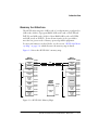
Figure 1-1 on page 1-3 shows the architecture of the ADSP-219x core. It
contains three independent computational units: the ALU, the multiplier/accumulator, and the shifter.
1-6
ADSP-219x/2192 DSP Hardware Reference