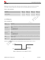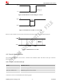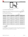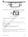
1
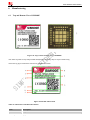
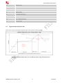
SIM900E_Hardware Design_V1.00
Smart Machine Smart Decision
Document Title
SIM900E Hardware Design
Version
1.00
Date
2013-02-02
Status
Release
Document Control ID
SIM900E_Hardware Design_V1.00
General Notes
SIMCom offers this information as a service to its customers, to support application and engineering efforts that
use the products designed by SIMCom. The information provided is based upon requirements specifically
provided to SIMCom by the customers. SIMCom has not undertaken any independent search for additional
relevant information, including any information that may be in the customer’s possession. Furthermore, system
validation of this product designed by SIMCom within a larger electronic system remains the responsibility of the
customer or the customer’s system integrator. All specifications supplied herein are subject to change.
Copyright
This document contains proprietary technical information which is the property of SIMCom Limited, copying of
this document and giving it to others and the using or communication of the contents thereof, are forbidden
without express authority. Offenders are liable to the payment of damages. All rights reserved in the event of grant
of a patent or the registration of a utility model or design. All specification supplied herein are subject to change
without notice at any time.
Copyright © Shanghai SIMCom Wireless Solutions Ltd. 2012
SIM900E_Hardware Design_V1.00
2
2013-02-02
Smart Machine Smart Decision
Contents
Contents.................................................................................................................................................................... 3
Version History ........................................................................................................................................................ 7
1
Introduction....................................................................................................................................................... 8
2
SIM900E Overview........................................................................................................................................... 8
2.1
SIM900E Key Features ............................................................................................................................ 8
2.2
Operating Modes .................................................................................................................................... 10
2.3
SIM900E Functional Diagram.................................................................................................................11
3
Package Information ...................................................................................................................................... 12
3.1
Pin out Diagram...................................................................................................................................... 12
3.2
Pin Description ....................................................................................................................................... 13
3.3
Package Dimensions............................................................................................................................... 15
4
Application Interface...................................................................................................................................... 18
4.1
Power Supply.......................................................................................................................................... 18
4.1.1 Minimizing Voltage Drop of VBAT ................................................................................................... 19
4.1.2 Monitoring Power Supply ................................................................................................................... 19
4.2
Power on/down Scenarios ...................................................................................................................... 19
4.2.1 Power on SIM900E ............................................................................................................................. 19
4.2.2 Power down SIM900E ........................................................................................................................ 20
4.2.3 Restart SIM900E by PWRKEY Pin .................................................................................................... 22
4.3
Power Saving Mode................................................................................................................................ 22
4.3.1 Minimum Functionality Mode ............................................................................................................ 22
4.3.2 Sleep Mode 1 (AT+CSCLK=1) .......................................................................................................... 23
4.3.3 Wake Up SIM900E from Sleep Mode 1 (AT+CSCLK=1)................................................................. 23
4.3.4 Sleep Mode 2 (AT+CSCLK=2) .......................................................................................................... 23
4.3.5 Wake Up SIM900E from Sleep Mode 2 (AT+CSCLK=2)................................................................. 24
4.4
RTC Backup ........................................................................................................................................... 24
4.5
Serial Interfaces ...................................................................................................................................... 25
4.5.1 Function of Serial Port and Debug Port .............................................................................................. 26
4.5.2 Software Upgrade and Debug ............................................................................................................. 27
4.6
Audio Interfaces ..................................................................................................................................... 27
4.6.1 Speaker Interface Configuration ......................................................................................................... 27
4.6.2 Microphone Interfaces Configuration ................................................................................................. 28
4.6.3 Earphone Interface Configuration....................................................................................................... 29
4.6.4 Audio Electronic Characteristics......................................................................................................... 29
4.7
SIM Card Interface ................................................................................................................................. 30
4.7.1 SIM Card Application ......................................................................................................................... 30
4.7.2 Design Considerations for SIM Card Holder ...................................................................................... 31
4.8
LCD Display/SPI Interface..................................................................................................................... 32
4.9
Keypad Interface .................................................................................................................................... 33
4.10
ADC........................................................................................................................................................ 34
4.11
RI Behaviors........................................................................................................................................... 34
4.12
Network Status Indication ...................................................................................................................... 35
SIM900E_Hardware Design_V1.00
3
2013-02-02
Smart Machine Smart Decision
4.13
4.14
4.15
4.16
4.17
General Purpose Input/Output (GPIO) ................................................................................................... 36
External Reset......................................................................................................................................... 36
PWM ...................................................................................................................................................... 37
I2C Bus.................................................................................................................................................... 38
Antenna Interface ................................................................................................................................... 38
5
Electrical, Reliability and Radio Characteristics......................................................................................... 39
5.1
Absolute Maximum Ratings................................................................................................................... 39
5.2
Recommended Operating Conditions..................................................................................................... 39
5.3
Digital Interface Characteristics ............................................................................................................. 39
5.4
SIM Card Interface Characteristics ........................................................................................................ 39
5.5
VDD_EXT Characteristics ..................................................................................................................... 40
5.6
SIM_VDD Characteristics...................................................................................................................... 40
5.7
VRTC Characteristics ............................................................................................................................. 40
5.8
Current Consumption (VBAT = 3.8V) ................................................................................................... 41
5.9
Radio Characteristics.............................................................................................................................. 42
5.9.1 Module RF Output Power ................................................................................................................... 42
5.9.2 Module RF Receive Sensitivity........................................................................................................... 43
5.9.3 Module Operating Frequencies ........................................................................................................... 43
6
Manufacturing ................................................................................................................................................ 44
6.1
Top and Bottom View of SIM900E........................................................................................................ 44
6.2
Typical Solder Reflow Profile................................................................................................................ 45
Appendix ................................................................................................................................................................ 47
A. Related Documents.......................................................................................................................................... 47
B. Terms and Abbreviations ................................................................................................................................. 48
C. Safety Caution ................................................................................................................................................. 49
SIM900E_Hardware Design_V1.00
4
2013-02-02
Smart Machine Smart Decision
Table Index
TABLE 1: SIM900E KEY FEATURES ............................................................................................................................. 8
TABLE 2: CODING SCHEMES AND MAXIMUM NET DATA RATES OVER AIR INTERFACE ............................ 10
TABLE 3: OVERVIEW OF OPERATING MODES........................................................................................................ 10
TABLE 4: PIN DESCRIPTION ....................................................................................................................................... 13
TABLE 5: THE CURRENT CONSUMPTION OF MINIMUM FUNCTIONALITY MODE ........................................ 23
TABLE 6: MICROPHONE INPUT CHARACTERISTICS ............................................................................................ 29
TABLE 7: AUDIO OUTPUT CHARACTERISTICS ...................................................................................................... 30
TABLE 8: PIN DESCRIPTION (AMPHENOL SIM CARD HOLDER)......................................................................... 31
TABLE 9: PIN DESCRIPTION (MOLEX SIM CARD HOLDER) ................................................................................ 32
TABLE 10: PIN DEFINITION OF THE KEYPAD INTERFACE................................................................................... 33
TABLE 11: ADC SPECIFICATION................................................................................................................................. 34
TABLE 12: RI BEHAVIORS ........................................................................................................................................... 34
TABLE 13: STATUS OF THE NETLIGHT PIN.............................................................................................................. 35
TABLE 14: PIN DEFINITION OF THE GPIO INTERFACE ......................................................................................... 36
TABLE 15: ABSOLUTE MAXIMUM RATINGS........................................................................................................... 39
TABLE 16: RECOMMENDED OPERATING CONDITIONS ....................................................................................... 39
TABLE 17: DIGITAL INTERFACE CHARACTERISTICS ........................................................................................... 39
TABLE 18: SIM CARD INTERFACE CHARACTERISTICS........................................................................................ 40
TABLE 19: VDD_EXT CHARACTERISTICS ............................................................................................................... 40
TABLE 20: SIM_VDD CHARACTERISTICS................................................................................................................ 40
TABLE 21: VRTC CHARACTERISTICS ....................................................................................................................... 40
TABLE 22: CURRENT CONSUMPTION* ..................................................................................................................... 41
TABLE 23: SIM900E GSM 900 AND GSM 850 CONDUCTED RF OUTPUT POWER.............................................. 42
TABLE 24: SIM900E DCS 1800 AND PCS 1900 CONDUCTED RF OUTPUT POWER ............................................ 42
TABLE 25: SIM900E CONDUCTED RF RECEIVE SENSITIVITY............................................................................. 43
TABLE 26: SIM900E OPERATING FREQUENCIES .................................................................................................... 43
TABLE 27: ILLUSTRATION OF MODULE INFORMATION ...................................................................................... 44
TABLE 28: RELATED DOCUMENTS ........................................................................................................................... 47
TABLE 29: TERMS AND ABBREVIATIONS................................................................................................................ 48
TABLE 30: SAFETY CAUTION..................................................................................................................................... 49
SIM900E_Hardware Design_V1.00
5
2013-02-02
Smart Machine Smart Decision
Figure Index
FIGURE 1: SIM900E FUNCTIONAL DIAGRAM ......................................................................................................... 11
FIGURE 2: SIM900E PIN OUT DIAGRAM (TOP VIEW)............................................................................................. 12
FIGURE 3: DIMENSIONS OF SIM900E(UNIT: MM) ............................................................................................. 15
FIGURE 4: RECOMMENDED PCB FOOTPRINT OUTLINE(UNIT: MM)............................................................ 16
FIGURE 5: RECOMMENDED SMT STENCIL OUTLINE(UNIT: MM)................................................................. 17
FIGURE 6: REFERENCE CIRCUIT OF THE LDO POWER SUPPLY ......................................................................... 18
FIGURE 7: REFERENCE CIRCUIT OF THE DC-DC POWER SUPPLY..................................................................... 18
FIGURE 8: VBAT VOLTAGE DROP DURING TRANSMIT BURST........................................................................... 19
FIGURE 9: THE MINIMAL VBAT VOLTAGE REQUIREMENT AT VBAT DROP .................................................... 19
FIGURE 10: POWERED ON/DOWN MODULE USING TRANSISTOR..................................................................... 19
FIGURE 11: POWERED ON/DOWN MODULE USING BUTTON ............................................................................. 20
FIGURE 12: TIMING OF POWER ON MODULE......................................................................................................... 20
FIGURE 13: TIMING OF POWER DOWN SIM900E BY PWRKEY............................................................................ 21
FIGURE 14: TIMING OF RESTART SIM900E.............................................................................................................. 22
FIGURE 15: RTC SUPPLY FROM CAPACITOR........................................................................................................... 24
FIGURE 16: RTC SUPPLY FROM NON-CHARGEABLE BATTERY ......................................................................... 24
FIGURE 17: RTC SUPPLY FROM RECHARGEABLE BATTERY .............................................................................. 24
FIGURE 18: SEIKO XH414H-IV01E CHARGE-DISCHARGE CHARACTERISTIC ................................................. 25
FIGURE 19: CONNECTION OF THE SERIAL INTERFACES..................................................................................... 25
FIGURE 20: CONNECTION OF RXD AND TXD ONLY ............................................................................................. 26
FIGURE 21: CONNECTION FOR SOFTWARE UPGRADING AND DEBUGGING.................................................. 27
FIGURE 22: SPEAKER REFERENCE CIRCUIT .......................................................................................................... 27
FIGURE 23: SPEAKER WITH AMPLIFIER REFERENCE CIRCUIT ......................................................................... 28
FIGURE 24 : MICROPHONE REFERENCE CIRCUIT................................................................................................. 28
FIGURE 25: EARPHONE REFERENCE CIRCUIT ....................................................................................................... 29
FIGURE 26: REFERENCE CIRCUIT OF THE 8-PIN SIM CARD HOLDER............................................................... 30
FIGURE 27: REFERENCE CIRCUIT OF THE 6-PIN SIM CARD HOLDER............................................................... 31
FIGURE 28: AMPHENOL C707 10M006 5122 SIM CARD HOLDER......................................................................... 31
FIGURE 29: MOLEX 91228 SIM CARD HOLDER ...................................................................................................... 32
FIGURE 30: REFERENCE CIRCUIT OF THE KEYPAD INTERFACE ....................................................................... 33
FIGURE 31: RI BEHAVIOUR OF VOICE CALLING AS A RECEIVER...................................................................... 34
FIGURE 32: RI BEHAVIOUR OF DATA CALLING AS A RECEIVER........................................................................ 35
FIGURE 33: RI BEHAVIOUR OF URC OR RECEIVE SMS ........................................................................................ 35
FIGURE 34: RI BEHAVIOUR AS A CALLER ............................................................................................................... 35
FIGURE 35: REFERENCE CIRCUIT OF NETLIGHT .................................................................................................. 36
FIGURE 36: RESET TIMING ......................................................................................................................................... 37
FIGURE 37: RESET REFERENCE DESIGN CIRCUIT ................................................................................................ 37
FIGURE 38: ANTENNA MATCHING CIRCUIT ........................................................................................................... 38
FIGURE 39: TOP, BOTTOM AND SIDE VIEW OF SIM900E ...................................................................................... 44
FIGURE 40: MODULE INFORMATION ....................................................................................................................... 44
FIGURE 41: STANDARD TEMPERATURE CURVE AND THE PARAMETER RANGE OF LEAD PROCESSES .. 45
FIGURE 42: STANDARD TEMPERATURE CURVE AND THE PARAMETER RANGE OF LEAD-FREE
PROCESSES............................................................................................................................................................ 46
SIM900E_Hardware Design_V1.00
6
2013-02-02
Smart Machine Smart Decision
Version History
Date
Version
Description of change
Author
2013-02-02
1.00
Origin
zhaojuntao
Tenglili
SIM900E_Hardware Design_V1.00
7
2013-02-02
Smart Machine Smart Decision
1
Introduction
This document describes SIM900E hardware interface in great detail.
This document can help users to quickly understand SIM900E interface specifications, electrical and mechanical
details. With the help of this document and other SIM900E application notes, user guide, users can use SIM900E
to design various applications quickly.
2
SIM900E Overview
Designed for global market, SIM900E is a quad-band GSM/GPRS module that works on frequencies GSM
850MHz, EGSM 900MHz, DCS 1800MHz and PCS 1900MHz. SIM900E features GPRS multi-slot class 10/
class 8 (optional) and supports the GPRS coding schemes CS-1, CS-2, CS-3 and CS-4.
With a tiny configuration of 19.8*19.8*2.7mm, SIM900E can meet almost all the space requirements in user
applications, such as M2M, smart phone, PDA and other mobile devices.
SIM900E has 69 pads in a LGA package , and provides all hardware interfaces between the module and
customers’ boards.
z
z
z
z
Serial port and debug port can help users to easily develop their applications.
Audio channel which includes a microphone input and a receiver output.
Programmable general purpose input and output.
The keypad and SPI display interfaces will give users the flexibility to develop customized applications.
SIM900E is designed with power saving technique so that the current consumption is as low as 1.0mA in sleep
mode.
SIM900E integrates TCP/IP protocol and extended TCP/IP AT commands which are very useful for data transfer
applications. For details about TCP/IP applications, please refer to document [2].
2.1
SIM900E Key Features
Table 1: SIM900E key features
Feature
Implementation
Power supply
3.2V ~ 4.8V
Power saving
Typical power consumption in sleep mode is 1.0mA ( BS-PA-MFRMS=9 )
z
Frequency bands
z
SIM900E_Hardware Design_V1.00
SIM900E Quad-band: GSM 850, EGSM 900, DCS 1800, PCS 1900.
SIM900E can search the 4 frequency bands automatically. The frequency
bands also can be set by AT command “AT+CBAND”. For details, please
refer to document [1].
Compliant to GSM Phase 2/2+
8
2013-02-02
Smart Machine Smart Decision
Transmitting power
z
z
Class 4 (2W) at GSM 850 and EGSM 900
Class 1 (1W) at DCS 1800 and PCS 1900
GPRS connectivity
z
z
GPRS multi-slot class 10(default)
GPRS multi-slot class 8 (option)
Temperature range
z
z
z
Normal operation: -30°C ~ +80°C
Restricted operation: -40°C ~ -30°C and +80 °C ~ +85°C*
Storage temperature -45°C ~ +90°C
Data GPRS
z
z
z
z
z
GPRS data downlink transfer: max. 85.6 kbps
GPRS data uplink transfer: max. 42.8 kbps
Coding scheme: CS-1, CS-2, CS-3 and CS-4
Integrate the TCP/IP protocol.
Support Packet Broadcast Control Channel (PBCCH)
CSD
z
Support CSD transmission
USSD
z
Unstructured Supplementary Services Data (USSD) support
SMS
z
z
MT, MO, CB, Text and PDU mode
SMS storage: SIM card
FAX
Group 3 Class 1
SIM interface
Support SIM card: 1.8V, 3V
External antenna
Antenna pad
Audio features
Speech codec modes:
z Half Rate (ETS 06.20)
z Full Rate (ETS 06.10)
z Enhanced Full Rate (ETS 06.50 / 06.60 / 06.80)
z Adaptive multi rate (AMR)
z Echo Cancellation
z Noise Suppression
z
Serial port and
debug port
z
z
z
z
z
z
z
*
Serial port:
Full modem interface with status and control lines, unbalanced,
asynchronous.
1200bps to 115200bps.
Can be used for AT commands or data stream.
Support RTS/CTS hardware handshake and software ON/OFF flow control.
Multiplex ability according to GSM 07.10 Multiplexer Protocol.
Autobauding supports baud rate from 1200 bps to 57600bps.
Debug port:
Null modem interface DBG_TXD and DBG_RXD.
Can be used for debugging and upgrading firmware.
Phonebook management
Support phonebook types: SM, FD, LD, RC, ON, MC.
SIM application toolkit
GSM 11.14 Release 99
Real time clock
Support RTC
Physical characteristics
Size: 19.8*19.8*2.7mm
Weight: 2.2g
Firmware upgrade
Firmware upgradeable by debug port.
SIM900E does work at this temperature, but some radio frequency characteristics may deviate from the GSM specification.
SIM900E_Hardware Design_V1.00
9
2013-02-02
Smart Machine Smart Decision
Table 2: Coding schemes and maximum net data rates over air interface
Coding scheme
1 timeslot
2 timeslot
4 timeslot
CS-1
9.05kbps
18.1kbps
36.2kbps
CS-2
13.4kbps
26.8kbps
53.6kbps
CS-3
15.6kbps
31.2kbps
62.4kbps
CS-4
21.4kbps
42.8kbps
85.6kbps
2.2
Operating Modes
The table below summarizes the various operating modes of SIM900E.
Table 3: Overview of operating modes
Mode
Normal
operation
Function
GSM/GPRS
SLEEP
Module will automatically go into sleep mode if the conditions of sleep
mode are enabling and there is no on air and no hardware interrupt (such as
GPIO interrupt or data on serial port).
In this case, the current consumption of module will reduce to the minimal
level.
In sleep mode, the module can still receive paging message and SMS.
GSM
IDLE
Software is active. Module registered to the GSM network, and the module
is ready to communicate.
GSM
TALK
Connection between two subscribers is in progress. In this case, the power
consumption depends on network settings such as DTX off/on,
FR/EFR/HR, hopping sequences, antenna.
GPRS
STANDBY
Module is ready for GPRS data transfer, but no data is currently sent or
received. In this case, power consumption depends on network settings and
GPRS configuration.
GPRS
DATA
There is GPRS data transfer (PPP or TCP or UDP) in progress. In this case,
power consumption is related with network settings (e.g. power control
level); uplink/downlink data rates and GPRS configuration (e.g. used
multi-slot settings).
Power down
Normal power down by sending the AT command “AT+CPOWD=1” or using the PWRKEY.
The power management unit shuts down the power supply for the baseband part of the
module, and only the power supply for the RTC is remained. Software is not active. The
serial port is not accessible. Power supply (connected to VBAT) remains applied.
Minimum
functionality
mode
AT command “AT+CFUN” can be used to set the module to a minimum functionality mode
without removing the power supply. In this mode, the RF part of the module will not work or
the SIM card will not be accessible, or both RF part and SIM card will be closed, and the
serial port is still accessible. The power consumption in this mode is lower than normal
mode.
SIM900E_Hardware Design_V1.00
10
2013-02-02
Smart Machine Smart Decision
2.3
SIM900E Functional Diagram
The following figure shows a functional diagram of SIM900E:
z The GSM baseband engine
z Flash
z The GSM radio frequency part
z The antenna interface
z The other interfaces
Figure 1: SIM900E functional diagram
SIM900E_Hardware Design_V1.00
11
2013-02-02
Smart Machine Smart Decision
3
3.1
Package Information
Pin out Diagram
Figure 2: SIM900E pin out diagram (Top view) SIM900E_Hardware Design_V1.00
12
2013-02-02
Smart Machine Smart Decision
3.2
Pin Description
Table 4: Pin description
Pin number
I/
Description
O
30,31,32
I
VRTC
43
I/
Power supply for RTC
O
It is recommended to
connect with a battery or
a capacitor (e.g. 4.7uF).
VDD_EXT
35
O 2.8V output power supply
If it is unused, keep open.
GND
1,4,7,9,18,25,26
,27,29,33,34,
61,62,63,64,65,
66,67,68,69
Ground
36
I
PWRKEY should be pulled low at least
1 second and then released to power
on/down the module.
I
Differential audio input
Pin name
Comment
Power supply
VBAT
Power supply
Power on/down
PWRKEY
Pulled up internally.
Audio interfaces
MIC_P
6
MIC_N
5
SPK_P
2
SPK_N
3
O Differential audio output
If these pins are unused,
keep open.
Status
STATUS
14
O Power on status
NETLIGHT
8
O Network status
If these pins are unused,
keep open.
LCD interface
DISP _CLK
57
O
DISP_DATA
59
I/
O Display interface
DISP _D/C
60
O
DISP _CS
58
O
If these pins are unused,
keep open.
2
I C interface
SDA
39
SCL
40
O
I2C serial bus data
I/ 2
I C serial bus clock
O
If these pins are unused,
keep open.
Keypad interface / GPIOs
GPIO5/KBR0
50
SIM900E_Hardware Design_V1.00
I/
GPIO5/keypad row 0
13
If these pins are unused,
2013-02-02
Smart Machine Smart Decision
GPIO4/KBR1
51
O GPIO4/keypad row 1
GPIO3/KBR2
53
GPIO3/keypad row 2
GPIO2/KBR3
52
GPIO2/keypad row 3
GPIO1/KBR4
46
GPIO1/keypad row 4
GPIO9/KBC1
47
GPIO9/keypad column 1
GPIO8/KBC2
45
GPIO8/keypad column 2
GPIO7/KBC3
49
GPIO7/keypad column 3
GPIO6/KBC4
48
GPIO6/keypad column 4
GPIO10
54
GPIO10
GPIO11
24
GPIO11
GPIO12
38
GPIO12
keep open.
Serial port
RXD
16
I
Receive data
TXD
17
O Transmit data
RTS
19
I
CTS
20
O Clear to send
DCD
23
O Data carrier detect
RI
22
O Ring indicator
DTR
21
I
DBG_TXD
42
O
DBG_RXD
41
I
SIM_VDD
13
O
SIM_DATA
11
I/
SIM data input/output
O
SIM_CLK
10
O SIM clock
SIM_RST
12
O SIM reset
SIM_PRESEN
CE
44
I
SIM card detection
If it is unused, keep open.
37
I
Input voltage range: 0V ~ 2.8V
If it is unused, keep open.
15
I
Reset input(Active low)
Recommend connecting
a 100nF capacitor.
Request to send
If these pins are unused,
keep open.
Data terminal ready
Debug interface
For debugging and upgrading firmware
If these pins are unused,
keep open.
SIM interface
Voltage supply for SIM card. Support
1.8V or 3V SIM card
All signals of SIM
interface
should
be
protected against ESD
with a TVS diode array.
ADC
ADC
External reset
NRESET
Pulse width modulation( PWM )
PWM1
56
O PWM
PWM2
55
O PWM
If these pins are unused,
keep open.
28
I/
RF antenna connection
O
Impendence must
controlled to 50Ω.
RF interface
RF_ANT
SIM900E_Hardware Design_V1.00
14
be
2013-02-02
Smart Machine Smart Decision
3.3
Package Dimensions
Figure 3: Dimensions of SIM900E(Unit: mm)
SIM900E_Hardware Design_V1.00
15
2013-02-02
Smart Machine Smart Decision
Figure 4: Recommended PCB footprint outline(Unit: mm)
SIM900E_Hardware Design_V1.00
16
2013-02-02
Smart Machine Smart Decision
Figure 5: Recommended SMT stencil outline(Unit: mm)
SIM900E_Hardware Design_V1.00
17
2013-02-02
Smart Machine Smart Decision
4
4.1
Application Interface
Power Supply
GND
The power supply range of SIM900E is from 3.2V to 4.8V. The transmitting burst will cause voltage drop and the
power supply must be able to provide sufficient current up to 2A. For the VBAT input, a bypass capacitor (low
ESR) such as a 100 µF is strongly recommended; this capacitor should be placed as close as possible to SIM900E
VBAT pins. The following figure is the reference design of +5V input power supply. The designed output for the
power supply is 4.1V, thus a linear regulator can be used.
Figure 6: Reference circuit of the LDO power supply
If there is a high drop-out between the input and the desired output (VBAT), a DC-DC power supply will be
preferable because of its better efficiency especially with the 2A peak current in burst mode of the module. The
following figure is the reference circuit.
Figure 7: Reference circuit of the DC-DC power supply
The single 3.6V Li-ion cell battery can be connected to SIM900E VBAT pins directly. But the Ni-Cd or Ni-MH
battery must be used carefully, since their maximum voltage can rise over the absolute maximum voltage of the
module and damage it.
When battery is used, the total impedance between battery and VBAT pins should be less than 150mΩ.
The following figure shows the VBAT voltage drop at the maximum power transmit phase, and the test condition
is as following:
VBAT=4.0V,
A VBAT bypass capacitor CA=100µF tantalum capacitor (ESR=0.7Ω),
Another VBAT bypass capacitor CB=1µF.
SIM900E_Hardware Design_V1.00
18
2013-02-02
Smart Machine Smart Decision
Figure 8: VBAT voltage drop during transmit burst
4.1.1
Minimizing Voltage Drop of VBAT
When designing the power supply in user’s application, pay special attention to power losses. Ensure that the
input voltage never drops below 3.1V even when current consumption rises to 2A in the transmit burst. If the
power voltage drops below 3.1V, the module may be shut down automatically. The PCB traces from the VBAT
pins to the power supply must be wide enough (at least 60mil) to decrease voltage drops in the transmit burst. The
power IC and the bypass capacitor should be placed to the module as close as possible.
Figure 9: The minimal VBAT voltage requirement at VBAT drop
4.1.2
Monitoring Power Supply
The AT command “AT+CBC” can be used to monitor the VBAT voltage. For detail, please refer to document [1].
4.2
4.2.1
Power on/down Scenarios
Power on SIM900E
User can power on SIM900E by pulling down the PWRKEY pin for at least 1 second and release. This pin is
already pulled up to 3V in the module internal, so external pull up is not necessary. Reference circuit is shown as
below.
Figure 10: Powered on/down module using transistor
SIM900E_Hardware Design_V1.00
19
2013-02-02
Smart Machine Smart Decision
Figure 11: Powered on/down module using button
The power on scenarios is illustrated as following figure.
Figure 12: Timing of power on module
When power on procedure is completed, SIM900E will send following URC to indicate that the module is ready
to operate at fixed baud rate.
RDY
This URC does not appear when autobauding function is active.
Note: User can use AT command “AT+IPR=x” to set a fixed baud rate and save the configuration to non-volatile flash memory.
After the configuration is saved as fixed baud rate, the Code “RDY” should be received from the serial port every time when
SIM900E is powered on. For details, please refer to the chapter “AT+IPR” in document [1].
4.2.2
Power down SIM900E
SIM900E will be powered down in the following situations:
z Normal power down procedure: power down SIM900E by the PWRKEY pin.
z Normal power down procedure: power down SIM900E by AT command “AT+CPOWD=1”.
z Abnormal power down: over-voltage or under-voltage automatic power down.
z Abnormal power down: over-temperature or under-temperature automatic power down.
4.2.2.1
Power down SIM900E by the PWRKEY Pin
User can power down SIM900E by pulling down the PWRKEY pin for at least 1 second and release. Please refer
to the power on circuit. The power down scenario is illustrated in following figure.
SIM900E_Hardware Design_V1.00
20
2013-02-02
Smart Machine Smart Decision
Figure 13: Timing of power down SIM900E by PWRKEY
This procedure makes the module log off from the network and allows the software to enter into a secure state to
save data before completely shut down.
Before the completion of the power down procedure, the module will send URC:
NORMAL POWER DOWN
At this moment, AT commands can not be executed any more, and only the RTC is still active. Power down mode
can also be indicated by STATUS pin, which is at low level at this time.
4.2.2.2
Power down SIM900E by AT Command
SIM900E can be powered down by AT command “AT+CPOWD=1”. This procedure makes the module log off
from the network and allows the software to enter into a secure state to save data before completely shut down.
Before the completion of the power down procedure, the module will send URC:
NORMAL POWER DOWN
At this moment, AT commands can not be executed any more, and only the RTC is still active. Power down mode
can also be indicated by STATUS pin, which is at low level at this time.
For detail about the AT command “AT+CPOWD”, please refer to document [1]
4.2.2.3
Over-voltage or Under-voltage Power down
The module software monitors the VBAT voltage constantly.
If the voltage ≤ 3.3V, the following URC will be reported:
UNDER-VOLTAGE WARNNING
If the voltage ≥ 4.7V, the following URC will be reported:
OVER-VOLTAGE WARNNING
If the voltage < 3.2V, the following URC will be reported, and the module will be automatically powered down.
UNDER-VOLTAGE POWER DOWN
If the voltage > 4.8V, the following URC will be reported, and the module will be automatically powered down.
OVER-VOLTAGE POWER DOWN
At this moment, AT commands can not be executed any more, and only the RTC is still active. Power down mode
can also be indicated by STATUS pin, which is at low level at this time.
SIM900E_Hardware Design_V1.00
21
2013-02-02
Smart Machine Smart Decision
4.2.2.4
Over-temperature or Under-temperature Power down
The module will constantly monitor the temperature of the module,
If the temperature > +80℃, the following URC will be reported:
+CMTE: 1
If the temperature < -30℃, the following URC will be reported:
+CMTE:-1
If the temperature > +85℃, the following URC will be reported, and the module will be automatically powered
down.
+CMTE: 2
If the temperature < -40℃, the following URC will be reported, and the module will be automatically powered
down.
+CMTE:-2
At this moment, AT commands can not be executed any more, and only the RTC is still active. Power down mode
can also be indicated by STATUS pin, which is at low level at this time.
The AT command “AT+CMTE” could be used to read the temperature when the module is running.
For details please refer to document [1].
4.2.3
Restart SIM900E by PWRKEY Pin
When the module works normally, if the user wants to restart the module, follow the procedure below:
1) Power down the module.
2) Wait for at least 800mS after STATUS pin changed to low level.
3) Power on the module.
Power down
Delay > 800mS
Restart
PWRKEY
STATUS
Figure 14: Timing of restart SIM900E
4.3
Power Saving Mode
SIM900E have two sleep modes: sleep mode 1 is enabled by hardware pin DTR; sleep mode 2 is only enabled by
serial port regardless of the DTR. In sleep mode, the current of module is very low. The AT command
“AT+CFUN=<fun>” can be used to set SIM900E into minimum functionality. When SIM900E is in sleep mode
and minimum functionality, the current of module is lowest.
4.3.1
Minimum Functionality Mode
There are three functionality modes, which could be set by the AT command “AT+CFUN=<fun>”. The command
provides the choice of the functionality levels <fun>=0,1,4.
SIM900E_Hardware Design_V1.00
22
2013-02-02
Smart Machine Smart Decision
z 0: minimum functionality.
z 1: full functionality (default).
z 4: flight mode (disable RF function).
Minimum functionality mode minimizes the current consumption to the lowest level. If SIM900E is set to
minimum functionality by “AT+CFUN=0”, the RF function and SIM card function will be disabled. In this case,
the serial port is still accessible, but all AT commands correlative with RF function and SIM card function will not
be accessible.
For detailed information about the AT Command “AT+CFUN=<fun>”, please refer to document [1].
Table 5: The Current consumption of Minimum Functionality Mode
<fun>
Current consumption(uA) (sleep mode)
0
651
1
1000
4
715
4.3.2
Sleep Mode 1 (AT+CSCLK=1)
User can control SIM900E module to enter or exit the sleep mode 1 (AT+CSCLK=1) by DTR signal. When DTR
is in high level and without interrupt (on air and hardware such as GPIO interrupt or data in serial port), SIM900E
will enter sleep mode 1 automatically. In this mode, SIM900E can still receive paging or SMS from network but
the serial port is not accessible.
Note: For SIM900E, it requests to set AT command “AT+CSCLK=1” and ensure DTR at high level to enable the sleep mode 1;
the default value is 0, which can not make the module to enter sleep mode. For more details please refer to document [1].
4.3.3
Wake Up SIM900E from Sleep Mode 1 (AT+CSCLK=1)
When SIM900E is in sleep mode 1 (AT+CSCLK=1), the following methods can wake up the module:
z Pull down DTR pin.
The serial port will be active after DTR pin is pulled to low level for about 50ms.
z Receive a voice or data call from network.
z Receive a SMS from network.
Note:If AT+CSCLK=1, it is requested to pull down DTR pin to enable the sleep mode ,else can not make the module to enter
sleep mode.
4.3.4
Sleep Mode 2 (AT+CSCLK=2)
In this mode, SIM900E will continuously monitor the serial port data signal. When there is no data transfer over 5
seconds on the RXD signal and there is no on air and hardware interrupts (such as GPIO interrupt), SIM900E will
enter sleep mode 2 automatically. In this mode, SIM900E can still receive paging or SMS from network but the
serial port is not accessible.
Note: For SIM900E, It is requested to set AT command “AT+CSCLK=2” to enable the sleep mode 2; the default value is 0, which
SIM900E_Hardware Design_V1.00
23
2013-02-02
Smart Machine Smart Decision
can not make the module to enter sleep mode. For more details please refer to document [1].
4.3.5
Wake Up SIM900E from Sleep Mode 2 (AT+CSCLK=2)
When SIM900E is in sleep mode 2 (AT+CSCLK=2), the following methods can wake up the module:
z Send data to SIM900E via main serial port. *
z Receive a voice or data call from network.
z Receive a SMS from network.
*
Note: The first byte of the user’s data will not be recognized.
4.4
RTC Backup
Current input for RTC when the VBAT is not supplied for the system. Current output for backup battery when
the VBAT power supply is in present and the backup battery is in low voltage state. The RTC power supply of
module can be provided by an external capacitor or a battery (non-chargeable or rechargeable) through the VRTC.
The following figures show various reference circuits for RTC back up.
z
External capacitor backup
Figure 15: RTC supply from capacitor
z
Non-chargeable battery backup
Figure 16: RTC supply from non-chargeable battery
z
Rechargeable battery backup
Figure 17: RTC supply from rechargeable battery
SIM900E_Hardware Design_V1.00
24
2013-02-02
Smart Machine Smart Decision
Coin-type rechargeable battery is recommended, such as XH414H-IV01E form Seiko can be used.
Typical charge-discharge curves for this battery are shown in the following figure.
Figure 18: Seiko XH414H-IV01E Charge-Discharge Characteristic
4.5
Serial Interfaces
SIM900E provides two unbalanced asynchronous serial ports. One is the serial port and the other is the debug port.
The module is designed as a DCE (Data Communication Equipment). The following figure shows the connection
between module and client (DTE).
MODULE (DCE)
CUSTOMER (DTE)
Serial port
Serial port1
TXD
TXD
RXD
RXD
RTS
RTS
CTS
CTS
DTR
DTR
DCD
DCD
RI
RING
Debug port
Serial port2
DBG_TX
TXD
DBG_RX
RXD
Figure 19: Connection of the serial interfaces
If only RXD and TXD are used in user’s application, other serial pins should be kept open. Please refer to
following figure.
SIM900E_Hardware Design_V1.00
25
2013-02-02
Smart Machine Smart Decision
MODULE (DCE)
CUSTOMER (DTE)
Serial port
Serial port1
TXD
TXD
RXD
RXD
RTS
RTS
CTS
CTS
DTR
DTR
DCD
DCD
RI
RING
Debug port
Serial port2
DBG_TX
TXD
DBG_RX
RXD
Figure 20: Connection of RXD and TXD only
4.5.1
Function of Serial Port and Debug Port
Serial port:
z Full modem device.
z Contains data lines TXD and RXD, hardware flow control lines RTS and CTS, status lines DTR, DCD and
RI.
z Serial port can be used for CSD FAX, GPRS service and AT communication. It can also be used for
multiplexing function. For details about multiplexing function, please refer to document [3].
z Serial port supports the following baud rates:
1200, 2400, 4800, 9600, 19200, 38400, 57600 and 115200bps
z Autobauding only supports the following baud rates:
1200, 2400, 4800, 9600, 19200, 38400 and 57600bps
z The default setting is autobauding.
Autobauding allows SIM900E to automatically detect the baud rate of the host device. Pay more attention to the
following requirements:
z Synchronization between DTE and DCE:
When DCE powers on with autobauding enabled, user must firstly send character “A” to synchronize the
baud rate. It is recommended to send “AT” until DTE receives the “OK” response, which means DTE and
DCE are correctly synchronized. For more information please refer to the AT command “AT+IPR”.
z Restrictions of autobauding operation:
The DTE serial port must be set at 8 data bits, no parity and 1 stop bit.
The URC such as "RDY", "+CFUN: 1" and "+CPIN: READY” will not be reported.
Note: User can use AT command “AT+IPR=x” to set a fixed baud rate and the setting will be saved to non-volatile flash
memory automatically. After the configuration is set as fixed baud rate, the URC such as "RDY", "+CFUN: 1" and "+CPIN:
READY” will be reported when SIM900E is powered on.
Debug port:
z Used for debugging and upgrading firmware.
z Debug port supports the baud rate of 115200bps.
SIM900E_Hardware Design_V1.00
26
2013-02-02
Smart Machine Smart Decision
4.5.2
Software Upgrade and Debug
Refer to the following figure for debugging and upgrading software.
Figure 21: Connection for software upgrading and debugging
The serial port and the debug port support the CMOS level. If user connects the module to the computer, the
level shifter should be added between the DCE and DTE.
For details about software upgrading,please refer to document [4].
4.6
Audio Interfaces
SIM900E provides one analog input, AIN, which could be used for electret microphone. The module also
provides one analog output, AOUT. The output can directly drive 32Ω receiver.
AT command “AT+CMIC” is used to adjust the input gain level of microphone. AT command “AT+SIDET” is
used to set the side-tone level. In addition, AT command “AT+CLVL” is used to adjust the output gain level. For
more details, please refer to document [1] and document [5].
In order to improve audio performance, the following reference circuits are recommended. The audio signals have
to be layout according to differential signal layout rules as shown in following figures. If user needs to use an
amplifier circuit for audio, National Semiconductor Company’s LM4890 is recommended.
4.6.1
Speaker Interface Configuration
Figure 22: Speaker reference circuit
SIM900E_Hardware Design_V1.00
27
2013-02-02
Smart Machine Smart Decision
Figure 23: Speaker with amplifier reference circuit
4.6.2
Microphone Interfaces Configuration
These components
should be placed to
microphone as close as
possible
ESD
ANTI
Electret
Microphone
10pF
33pF
10pF
33pF
The lines in bold type should
be accorded to differential
signal layout rules
MIC_P
MODULE
MIC_N
ESD
ANTI
10pF
33pF
Figure 24 : Microphone reference circuit
Microphone input also could be used to LINE-IN input. For details, please refer to document [6].
SIM900E_Hardware Design_V1.00
28
2013-02-02
Smart Machine Smart Decision
4.6.3
Earphone Interface Configuration
Figure 25: Earphone reference circuit
4.6.4
Audio Electronic Characteristics
Table 6: Microphone Input Characteristics
Parameter
Min
Typ
Max
Unit
Working Voltage
1.2
1.5
2.0
V
Working Current
200
500
uA
External Microphone Load Resistance
1.2
2.2
Internal biasing DC Characteristics
Differential input
voltage
kΩ
2.5
V
THD <1% at
F=1KHz; pre-amp
gain = 20 dB;
PGA gain = 14 dB
15.9
mVrms
THD <5% at
F=1KHz;pre-amp
gain = 0 dB; PGA
gain = 0 dB
740
mVrms
SIM900E_Hardware Design_V1.00
29
2013-02-02
Smart Machine Smart Decision
Table 7: Audio Output Characteristics
Parameter
Normal
Output(SPK)
4.7
4.7.1
Conditions
Min
Typ
Max
Unit
RL=32Ω
THD=0.1%
-
91
-
mW
RL=32Ω
THD=1%
-
96
-
mW
Output swing
Voltage
(single ended)
1.1
Vpp
Output swing
Voltage
(differential)
2.2
Vpp
SIM Card Interface
SIM Card Application
The SIM interface complies with the GSM Phase 1 specification and the new GSM Phase 2+ specification for
FAST 64 kbps SIM card. Both 1.8V and 3.0V SIM card are supported. The SIM interface is powered from an
internal regulator in the module.
It is recommended to use an ESD protection component such as ST (www.st.com ) ESDA6V1W5 or ON SEMI
(www.onsemi.com ) SMF05C.The pull up resistor (15KΩ) on the SIM_DATA line is already added in the module
internal. Note that the SIM peripheral circuit should be close to the SIM card socket. The reference circuit of the
8-pin SIM card holder is illustrated in the following figure.
Figure 26: Reference circuit of the 8-pin SIM card holder
The SIM_PRESENCE pin is used for detection of the SIM card hot plug in. User can select the 8-pin SIM card
holder to implement SIM card detection function. AT command “AT+CSDT” is used to enable or disable SIM
card detection function. For details of this AT command, please refer to document [1].
If the SIM card detection function is not used, user can keep the SIM_PRESENCE pin open. The reference
circuit of 6-pin SIM card holder is illustrated in the following figure.
SIM900E_Hardware Design_V1.00
30
2013-02-02
Smart Machine Smart Decision
Figure 27: Reference circuit of the 6-pin SIM card holder
4.7.2
Design Considerations for SIM Card Holder
For 6-pin SIM card holder, SIMCom recommends to use Amphenol C707 10M006 5122 .User can visit
http://www.amphenol.com for more information about the holder.
Figure 28: Amphenol C707 10M006 5122 SIM card holder
Table 8: Pin description (Amphenol SIM card holder)
Pin name
Signal
Description
C1
SIM_VDD
SIM card power supply
C2
SIM_RST
SIM card reset
C3
SIM_CLK
SIM card clock
C5
GND
Connect to GND
C6
VPP
Not connect
C7
SIM_DATA
SIM card data I/O
SIM900E_Hardware Design_V1.00
31
2013-02-02
Smart Machine Smart Decision
For 8 pins SIM card holder, SIMCom recommends to use Molex 91228.User can visit http://www.molex.com for
more information about the holder.
Figure 29: Molex 91228 SIM card holder
Table 9: Pin description (Molex SIM card holder)
Pin name
Signal
Description
C1
SIM_VDD
SIM card power supply
C2
SIM_RST
SIM card reset
C3
SIM_CLK
SIM card clock
C4
GND
Connect to GND
C5
GND
Connect to GND
C6
VPP
Not connect
C7
SIM_DATA
SIM card data I/O
C8
SIM_PRESENCE
Detect SIM card presence
4.8
LCD Display/SPI Interface
SIM900E provides a serial LCD display interface. It could also be used as SPI interface in the embedded AT
application. For details about embedded AT application, please refer to document [7].
SIM900E_Hardware Design_V1.00
32
2013-02-02
Smart Machine Smart Decision
Note: This function is not supported in the standard firmware. If user wants this function, the firmware must be customized.
Please contact SIMCom for more details.
4.9
Keypad Interface
The keypad interface consists of 4 keypad column outputs and 5 keypad row inputs. The basic configuration is 4
keypad columns and 5 keypad rows, total 20 keys.
Table 10: Pin definition of the keypad interface
Pin name
Pin number
Default function
Second function
Default state
GPIO1/ KBR4
46
GPIO1
GPIO2/ KBR3
52
GPIO2
GPIO3/ KBR2
53
GPIO3
GPIO4/ KBR1
51
GPIO4
GPIO5/ KBR0
50
GPIO5
Input, Pull down
GPIO6/ KBC4
48
GPIO6
Input, Pull down
GPIO7/ KBC3
49
GPIO7
GPIO8/ KBC2
45
GPIO8
GPIO9/ KBC1
47
GPIO9
Input, Pull down
Keypad matrix
column
Keypad matrix row
Input, Pull down
Input, Pull down
Input, Pull down
Input, Pull down
Input, Pull down
Input, Pull down
The keypad interface allows a direct external matrix connection. A typical recommended circuit of the keypad is
shown in the following figure.
Figure 30: Reference circuit of the keypad interface
Note: This function is not supported in the standard firmware. If user wants this function, the firmware must be customized.
Please contact SIMCom for more details.
SIM900E_Hardware Design_V1.00
33
2013-02-02
Smart Machine Smart Decision
4.10 ADC
SIM900E provides an auxiliary ADC, which can be used to measure the voltage. User can use AT command
“AT+CADC” to read the voltage value. For details of this AT command, please refer to document [1].
Table 11: ADC specification
Parameter
Min
Typ
Max
Unit
Voltage range
0
-
2.8
V
ADC Resolution
-
10
-
bits
Sampling rate
-
-
200K
Hz
4.11 RI Behaviors
Table 12: RI Behaviors
State
RI response
Standby
High
Voice call
The pin is changed to low. When any of the following events occur, the pin will be changed
to high:
(1)Establish the call
(2)Hang up the call
Data call
The pin is changed to low. When any of the following events occur, the pin will be changed
to high:
(1)Establish the call
(2)Hang up the call
SMS
The pin is changed to low, and kept low for 120ms when a SMS is received. Then it is
changed to high.
URC
The pin is changed to low, and kept low for 120ms when some URCs are reported. Then it is
changed to high. For more details, please refer to document [8].
The behavior of the RI pin is shown in the following figure when the module is used as a receiver.
Figure 31: RI behaviour of voice calling as a receiver
SIM900E_Hardware Design_V1.00
34
2013-02-02
Smart Machine Smart Decision
RI
HIGH
Establish the call
Hang up the call
LOW
Idle
Ring
Figure 32: RI behaviour of data calling as a receiver
Figure 33: RI behaviour of URC or receive SMS
However, if the module is used as caller, the RI will remain high. Please refer to the following figure.
Figure 34: RI behaviour as a caller
4.12 Network Status Indication
The NETLIGHT pin can be used to drive a network status indication LED. The status of this pin is listed in
following table:
Table 13: Status of the NETLIGHT pin
Status
SIM900E behavior
Off
SIM900E is not running
64ms On/ 800ms Off
SIM900E not registered the network
64ms On/ 3000ms Off
SIM900E registered to the network
64ms On/ 300ms Off
GPRS communication is established
A reference circuit is recommended in the following figure:
SIM900E_Hardware Design_V1.00
35
2013-02-02
Smart Machine Smart Decision
Figure 35: Reference circuit of NETLIGHT
4.13 General Purpose Input/Output (GPIO)
SIM900E provides up to 12 GPIO pins. The output voltage level of the GPIO can be set by the AT command
“AT+ SGPIO”. The input voltage level of the GPIO can also be read by the AT command “AT+ SGPIO”. For
more details, please refer to document [1].
Table 14: Pin definition of the GPIO interface
Pin name
Pin number
Default function
Second function
Default state
GPIO1/ KBR4
46
GPIO1
KBR4
input, pull down
GPIO2/ KBR3
52
GPIO2
KBR3
input, pull down
GPIO3/ KBR2
53
GPIO3
KBR2
input, pull down
GPIO4/ KBR1
51
GPIO4
KBR1
input, pull down
GPIO5/ KBR0
50
GPIO5
KBR0
input, pull down
GPIO6/ KBC4
48
GPIO6
KBC4
input, pull down
GPIO7/ KBC3
49
GPIO7
KBC3
input, pull down
GPIO8/ KBC2
45
GPIO8
KBC2
input, pull down
GPIO9/ KBC1
47
GPIO9
KBC1
input, pull down
GPIO10
54
GPIO10
input, pull up
GPIO11
24
GPIO11
input, pull down
GPIO12
38
GPIO12
input, pull down
4.14 External Reset
The external NRESET pin is used to reset the module. This function is used as an emergency reset only when AT
command “AT+CPOWD=1” and the PWRKEY pin have no effect. The NRESET pin could be pulled down to
reset the module. The reset timing is illustrated in the following figure.
SIM900E_Hardware Design_V1.00
36
2013-02-02
Smart Machine Smart Decision
Figure 36: Reset timing
This pin is already pulled up in the module, so the external pull-up resistor is not necessary. A 100nF capacitor
close to the NRESET pin is strongly recommended. A reference circuit is shown in the following figure.
Figure 37: Reset reference design circuit
NOTE: It is recommended to cut off the VBAT power supply directly instead of using external reset pin when SIM900E can not
respond to the AT command “AT+CPOWD=1” and PWRKEY pin.
4.15 PWM
SIM900E provides two PWMs. PWM2 can be used to drive a vibrator, and a backlight LED for display or
keyboard.
PWM2 output frequency varies from 25.6KHz to 3.25MHz.Two 7-bit unsigned binary parameters are used for the
output period and for the duty cycle.
PWM1 is intend for controlling a buzzer.
Features of PWM1:
z 10-bit resolution for buzzer tone frequency generation from 200 Hz to 5 kHz
z Tone frequency error < 1 % for all standard piano notes from 200 Hz to 5 kHz
z Tone level control from 0 dB down to −24 dB in +4 dB steps
z Audio mute
PWM1 outputs a square wave at the desired tone frequency. The tone frequencies are programmable from 200 Hz
to 5 kHz and can be re-programmed on-the-fly to generate monophonic audio ring tones or alert tones. The tone
level can be adjusted over a 24 dB range in 4 dB steps, or it can be muted.
The AT command “AT + SPWM” is used to set the output period and duty cycle of the PWMs. For details,please
refer to document [1].
SIM900E_Hardware Design_V1.00
37
2013-02-02
Smart Machine Smart Decision
4.16 I2C Bus
The SIM900E provides an I2C interface which is only used in the embedded AT application.
Note: This function is not supported in the standard firmware. If user wants this function, the firmware must be customized.
Please contact SIMCom for more details.
4.17 Antenna Interface
SIM900E provides a RF antenna interface. The customer’s antenna should be located in the customer’s main
board and connected to the module’s antenna pad through microstrip line or other type RF traces which
impendence must be controlled to 50Ω. To facilitate the antenna tuning and certification test, a RF connector and
an antenna matching circuit should be added. The following figure is the recommended circuit.
MODULE
GND
RF_ANT
GND
59
RF test connector
Matching circuit
60
61
R101
J102
C101
R102
Antenna feed pad
J101
C102
Figure 38: Antenna matching circuit
In this figure, the components R101,R102,C101 and C102 are used for antenna matching, the components’ values
only can be got after the antenna tuning. Usually, matching components’ values are provided by antenna vendor.
The default values of R101 and R102 are 0Ω, and reserve the places of C101 and C102 without soldering.
The RF connector in above figure is used for conducted RF performance test, and should be placed as close as
possible to the module’s RF_ANT pin. The traces in bold type in above figure should be treated as 50Ω
impedance controlled line in PCB layout. For details about radio frequency trace layout, please refer to document
[9].
SIM900E_Hardware Design_V1.00
38
2013-02-02
Smart Machine Smart Decision
5
Electrical, Reliability and Radio Characteristics
5.1
Absolute Maximum Ratings
The absolute maximum ratings stated in following table are stress ratings under non-operating conditions. Stresses
beyond any of these limits will cause permanent damage to SIM900E.
Table 15: Absolute maximum ratings
*
Symbol
Parameter
Min
Typ
Max
Unit
VBAT
Power supply voltage
-
-
5.5
V
VI*
Input voltage
-0.3
-
3.1
V
II
*
Input current
-
-
10
mA
IO*
Output current
-
-
10
mA
2
These parameters are for digital interface pins, such as keypad, GPIO, I C, UART, LCD, PWMs and DEBUG.
5.2
Recommended Operating Conditions
Table 16: Recommended operating conditions
Symbol
Parameter
Min
Typ
Max
Unit
VBAT
Power supply voltage
3.2
4.0
4.8
V
TOPER
Operating temperature
-40
+25
+85
℃
TSTG
Storage temperature
-45
+90
℃
5.3
Digital Interface Characteristics
Table 17: Digital interface characteristics Symbol
Parameter
Min
Typ
Max
Unit
IIH
High-level input current
-10
-
10
uA
IIL
Low-level input current
-10
-
10
uA
VIH
High-level input voltage
2.4
-
-
V
VIL
Low-level input voltage
-
-
0.4
V
VOH
High-level output voltage
2.7
-
-
V
VOL
Low-level output voltage
-
-
0.1
V
* These parameters are for digital interface pins, such as keypad, GPIO, I2C, UART, LCD, PWMs and DEBUG.
5.4
SIM Card Interface Characteristics
SIM900E_Hardware Design_V1.00
39
2013-02-02
Smart Machine Smart Decision
Table 18: SIM card interface characteristics Symbol
Parameter
Min
Typ
Max
Unit
IIH
High-level input current
-10
-
10
uA
IIL
Low-level input current
-10
-
10
uA
VIH
High-level input voltage
1.4
-
-
V
2.4
-
-
V
VIL
Low-level input voltage
-
-
0.4
V
2.4
V
VOH
High-level output voltage
VOL
Low-level output voltage
5.5
1.7
-
-
V
2.7
-
-
V
-
-
0.1
V
-
-
0.1
V
VDD_EXT Characteristics
Table 19: VDD_EXT characteristics
Symbol
Parameter
Min
Typ
Max
Unit
VO
Output voltage
2.70
2.80
2.95
V
IO
Output current
-
-
10
mA
Min
Typ
Max
Unit
2.75
2.9
3.00
1.65
1.80
1.95
-
-
10
mA
5.6
SIM_VDD Characteristics
Table 20: SIM_VDD characteristics Symbol
Parameter
VO
Output voltage
IO
Output current
5.7
VRTC Characteristics
V
Table 21: VRTC characteristics Symbol
Parameter
Min
Typ
Max
Unit
VRTC-IN
VRTC input voltage
2.00
3.00
3.15
V
IRTC-IN
VRTC input current
-
2
-
uA
VRTC-OUT
VRTC output voltage
-
3.00
-
V
IRTC-OUT
VRTC output current
-
10
-
uA
SIM900E_Hardware Design_V1.00
40
2013-02-02
Smart Machine Smart Decision
5.8
Current Consumption (VBAT = 3.8V)
Table 22: Current consumption* Symbol
Parameter
Conditions
Value
Unit
IVRTC
VRTC current
VBAT disconnects. Backup battery is 3 V
2
uA
Power down mode
30
uA
Sleep mode
BS-PA-MFRMS=9
1.0
BS-PA-MFRMS=5
1.2
BS-PA-MFRMS=2
1.5
mA
GSM 850
Idle mode
EGSM 900
22
DCS 1800
mA
PCS 1900
GSM 850
EGSM 900
Voice call
DCS 1800
PCS 1900
IVBAT
VBAT current
Data mode
GPRS(1Rx,1Tx)
Data mode
GPRS(4Rx,1Tx)
Data mode
GPRS(3Rx,2Tx)
IVBAT-peak
Peak current
GSM 850
EGSM 900
DCS 1800
PCS 1900
GSM 850
EGSM 900
DCS 1800
PCS 1900
GSM 850
EGSM 900
DCS 1800
PCS 1900
During Tx burst
PCL=5
240
PCL=12
108
PCL=19
81
PCL=0
176
PCL=7
94
PCL=15
76
PCL=5
240
PCL=12
110
PCL=19
83
PCL=0
170
PCL=7
95
PCL=15
80
PCL=5
223
PCL=12
150
PCL=19
120
PCL=0
166
PCL=7
130
PCL=15
115
PCL=5
410
PCL=12
185
PCL=19
130
PCL=0
300
PCL=7
155
PCL=15
122
2
mA
mA
mA
mA
mA
mA
mA
A
* In above table the current consumption value is the typical one of the module tested in laboratory. In the mass production stage,
there may be differences among each individual.
SIM900E_Hardware Design_V1.00
41
2013-02-02
Smart Machine Smart Decision
5.9
5.9.1
Radio Characteristics
Module RF Output Power
The following table shows the module conducted output power, it is followed by the 3GPP TS 05.05 technical
specification requirement.
Table 23: SIM900E GSM 900 and GSM 850 conducted RF output power
GSM 900 and EGSM 850
PCL
Tolerance (dB) for conditions
Nominal output power (dBm)
Normal
Extreme
5
33
±3
±4
6
31
±3
±4
7
29
±3
±4
8
27
±3
±4
9
25
±3
±4
10
23
±3
±4
11
21
±3
±4
12
19
±3
±4
13
17
±3
±4
14
15
±3
±4
15
13
±3
±4
16
11
±5
±6
17
9
±5
±6
18
7
±5
±6
19-31
5
±5
±6
Table 24: SIM900E DCS 1800 and PCS 1900 conducted RF output power
DCS 1800 and PCS 1900
PCL
Tolerance (dB) for conditions
Nominal output power (dBm)
Normal
Extreme
0
30
±3
±4
1
28
±3
±4
2
26
±3
±4
3
24
±3
±4
4
22
±3
±4
5
20
±3
±4
6
18
±3
±4
7
16
±3
±4
8
14
±3
±4
9
12
±4
±5
SIM900E_Hardware Design_V1.00
42
2013-02-02
Smart Machine Smart Decision
10
10
±4
±5
11
8
±4
±5
12
6
±4
±5
13
4
±4
±5
14
2
±5
±6
15-28
0
±5
±6
For the module’s output power, the following is should be noted:
At GSM900 and GSM850 band, the module is a class 4 device, so the module’s output power should not exceed
33dBm, and at the maximum power level, the output power tolerance should not exceed +/-2dB under normal
condition and +/-2.5dB under extreme condition.
At DCS1800 and PCS1900 band, the module is a class 1 device, so the module’s output power should not exceed
30dBm, and at the maximum power level, the output power tolerance should not exceed +/-2dB under normal
condition and +/-2.5dB under extreme condition.
5.9.2
Module RF Receive Sensitivity
The following table shows the module’s conducted receive sensitivity, it is tested under static condition.
Table 25: SIM900E conducted RF receive sensitivity
Frequency
Receive sensitivity(Typical)
Receive sensitivity(Max)
GSM850
-109dBm
-107dBm
EGSM900
-109dBm
-107dBm
DCS1800
-109dBm
-107dBm
PCS1900
-109dBm
-107dBm
5.9.3
Module Operating Frequencies
The following table shows the module’s operating frequency range; it is followed by the 3GPP TS 05.05 technical
specification requirement.
Table 26: SIM900E operating frequencies
Frequency
Receive
Transmit
GSM850
869 ~ 894MHz
824 ~ 849 MHz
EGSM900
925 ~ 960MHz
880 ~ 915MHz
DCS1800
1805 ~ 1880MHz
1710 ~ 1785MHz
PCS1900
1930 ~ 1990MHz
1850 ~ 1910MHz
SIM900E_Hardware Design_V1.00
43
2013-02-02
Smart Machine Smart Decision
6
Manufacturing
6.1
Top and Bottom View of SIM900E
Figure 39: Top, bottom and side view of SIM900E
Note: These test points are only used for module manufacturing and testing. They are not for customer using.
The following figure marked the information of SIM900E module.
Figure 40: Module information
Table 27: illustration of module information
Item
Description
A
Logo of SIMCom
SIM900E_Hardware Design_V1.00
44
2013-02-02
Smart Machine Smart Decision
B
Module name
C
Module part number
D
Module serial number
E
Module IMEI
F
CE authenticated logo
G
2-dimensional bar code
H
FCC authenticated logo
J
First pin mark
6.2
Typical Solder Reflow Profile
Please refer to the recommended ramp-soak-spike reflow profile as following shows
Figure 41: Standard temperature curve and the parameter range of lead processes
SIM900E_Hardware Design_V1.00
45
2013-02-02
Smart Machine Smart Decision
Figure 42: Standard temperature curve and the parameter range of lead-free processes
SIM900E_Hardware Design_V1.00
46
2013-02-02
Smart Machine Smart Decision
Appendix
A. Related Documents
Table 28: Related documents
SN
Document name
Remark
[1]
SIM900_AT
Manual
SIM900 AT Command Manual
[2]
AN_SIM900_TCPIP
TCP/IP Applications User Manual
[3]
SIM900_Multiplexer User
Manual_Application Note
SIM900 Multiplexer User Manual Application Note
[4]
AN_SIM900
Series_Update Tool_UGD
SIM900 Series Update Tool User Guide
[5]
AN_SIM900_AUDIO
Applications Note About SIM900 Audio
[6]
AN_Serial Port
Application Note About Serial Port
[7]
AN_SIM900E-TE PCB
Layout & Schematic for
Reference
Application Note About SIM900E-TE PCB Layout & Schematic
[8]
ITU-T
Draft
new
recommendation V.25ter:
Serial asynchronous automatic dialing and control
[9]
GSM 07.07:
Digital cellular telecommunications (Phase 2+); AT command set for GSM
Mobile Equipment (ME)
[10]
GSM 07.10:
Support GSM 07.10 multiplexing protocol
[11]
GSM 07.05:
Digital cellular telecommunications (Phase 2+); Use of Data Terminal
Equipment – Data Circuit terminating Equipment (DTE – DCE) interface
for Short Message Service (SMS) and Cell Broadcast Service (CBS)
[12]
GSM 11.14:
Digital cellular telecommunications system (Phase 2+); Specification of
the SIM Application Toolkit for the Subscriber Identity Module – Mobile
Equipment (SIM – ME) interface
[13]
GSM 11.11:
Digital cellular telecommunications system (Phase 2+); Specification of
the Subscriber Identity Module – Mobile Equipment (SIM – ME) interface
[14]
GSM 03.38:
Digital cellular telecommunications system (Phase 2+); Alphabets and
language-specific information
[15]
GSM 11.10
Digital cellular telecommunications system (Phase 2); Mobile Station
(MS) conformance specification; Part 1: Conformance specification
Command
SIM900E_Hardware Design_V1.00
47
2013-02-02
Smart Machine Smart Decision
B. Terms and Abbreviations
Table 29: Terms and Abbreviations
Abbreviation
Description
ADC
Analog-to-Digital Converter
AMR
Adaptive Multi-Rate
CS
Coding Scheme
CSD
Circuit Switched Data
CTS
Clear to Send
DTE
Data Terminal Equipment (typically computer, terminal, printer)
DTR
Data Terminal Ready
DTX
Discontinuous Transmission
EFR
Enhanced Full Rate
EGSM
Enhanced GSM
ESD
Electrostatic Discharge
ETS
European Telecommunication Standard
FR
Full Rate
GPRS
General Packet Radio Service
GSM
Global Standard for Mobile Communications
HR
Half Rate
IMEI
International Mobile Equipment Identity
Li-ion
Lithium-Ion
MO
Mobile Originated
MS
Mobile Station (GSM engine), also referred to as TE
MT
Mobile Terminated
PAP
Password Authentication Protocol
PBCCH
Packet Broadcast Control Channel
PCB
Printed Circuit Board
PCL
Power Control Level
PCS
Personal Communication System, also referred to as GSM 1900
PDU
Protocol Data Unit
PPP
Point-to-point protocol
RF
Radio Frequency
RMS
Root Mean Square (value)
RTC
Real Time Clock
RX
Receive Direction
SIM
Subscriber Identification Module
SMS
Short Message Service
TE
Terminal Equipment, also referred to as DTE
TX
Transmit Direction
SIM900E_Hardware Design_V1.00
48
2013-02-02
Smart Machine Smart Decision
UART
Universal Asynchronous Receiver & Transmitter
URC
Unsolicited Result Code
USSD
Unstructured Supplementary Service Data
Phonebook abbreviations
FD
SIM fix dialing phonebook
LD
SIM last dialing phonebook (list of numbers most recently dialed)
MC
Mobile Equipment list of unanswered MT calls (missed calls)
ON
SIM (or ME) own numbers (MSISDNs) list
RC
Mobile Equipment list of received calls
SM
SIM phonebook
NC
Not connect
C. Safety Caution
Table 30: Safety caution
Marks
Requirements
When in a hospital or other health care facility, observe the restrictions about the use of mobiles.
Switch the cellular terminal or mobile off, medical equipment may be sensitive to not operate
normally for RF energy interference.
Switch off the cellular terminal or mobile before boarding an aircraft. Make sure it is switched off.
The operation of wireless appliances in an aircraft is forbidden to prevent interference with
communication systems. Forget to think much of these instructions may lead to the flight safety or
offend against local legal action, or both.
Do not operate the cellular terminal or mobile in the presence of flammable gases or fumes. Switch
off the cellular terminal when you are near petrol stations, fuel depots, chemical plants or where
blasting operations are in progress. Operation of any electrical equipment in potentially explosive
atmospheres can constitute a safety hazard.
Your cellular terminal or mobile receives and transmits radio frequency energy while switched on.
RF interference can occur if it is used close to TV sets, radios, computers or other electric
equipment.
Road safety comes first! Do not use a hand-held cellular terminal or mobile when driving a
vehicle, unless it is securely mounted in a holder for hands free operation. Before making a call
with a hand-held terminal or mobile, park the vehicle.
GSM cellular terminals or mobiles operate over radio frequency signals and cellular networks and
cannot be guaranteed to connect in all conditions, for example no mobile fee or a invalid SIM card.
While you are in this condition and need emergent help, please remember using emergency calls.
In order to make or receive calls, the cellular terminal or mobile must be switched on and in a
service area with adequate cellular signal strength.
Some networks do not allow for emergency call if certain network services or phone features are in
use (e.g. lock functions, fixed dialing etc.). You may have to deactivate those features before you
can make an emergency call.
Also, some networks require that a valid SIM card be properly inserted in the cellular terminal or
mobile.
SIM900E_Hardware Design_V1.00
49
2013-02-02
Smart Machine Smart Decision
Contact us:
Shanghai SIMCom Wireless Solutions Ltd.
Add: SIM Technology Building,No.633,Jinzhong Road,Changning District,Shanghai P.R. China
200335
Tel: +86 21 3235 3300
Fax: +86 21 3235 3301
URL: www.sim.com/wm
SIM900E_Hardware Design_V1.00
50
2013-02-02