1
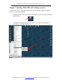
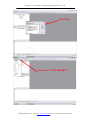
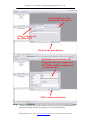
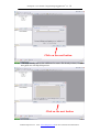
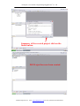
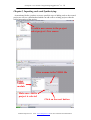
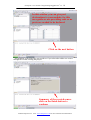
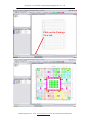
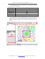
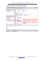
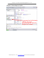
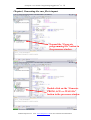
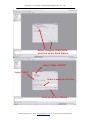
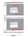
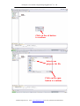
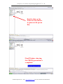
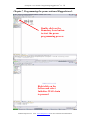
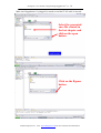
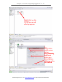
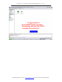
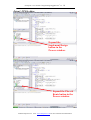
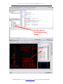
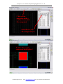
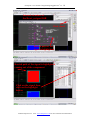
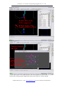
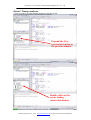
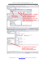
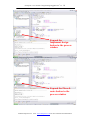
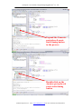
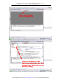
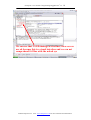
Enterpoint’s User manual “Programming Raggedstone1” rev 1.0
Enterpoint
FPGA and ASIC Design
Programming Raggedstone1 User Guide, (Rev1.0)
This user guide will take the user through some simple easy steps on how to program
Raggedstone1 through the platform flash using Xilinx’s non-volatile programming
proms fitted onboard, the format of this guide is visual using screenshots for much of
the flow and explanation.
STEPS TO UNDERTAKE:
1.
Opening Xilinx ISE and creating a project,
2.
Inputting code and synthesizing,
3.
Assigning package pins to the design,
4.
Place and routing the Design,
5.
Generating the .bit file,
6.
Generating the .mcs prom file in impact,
7.
Programming the proms onboard Raggedstone1,
8.
Testing the functionality of the design.
User Guide AIMS:
The aims of this user guide are to give the user a basic understanding of how to go
about generating a working functional design in ISE and implementing the design
onto a real hardware platform.
©2006 Enterpoint Ltd. Visit: www.enterpoint.co.uk for more materials and information
Enterpoint’s User manual “Programming Raggedstone1” rev 1.0
Chapter1, Opening Xilinx ISE and creating a project.
There are two ways to open Xilinx ISE, these are through the windows navigation
structure or of the users desktop.
•
Desktop, double click on the Xilinx ISE shortcut icon on the desktop (default
install feature)
•
Navigation, Click on the Project Navigator icon under the Xilinx ISE 8.?.?
menu under “ALL PROGRAMS”.
©2006 Enterpoint Ltd. Visit: www.enterpoint.co.uk for more materials and information
Enterpoint’s User manual “Programming Raggedstone1” rev 1.0
Click OK
Select file-> NEW PROJECT
©2006 Enterpoint Ltd. Visit: www.enterpoint.co.uk for more materials and information
Enterpoint’s User manual “Programming Raggedstone1” rev 1.0
Select Desktop as the
location for the project
Select A Name for
the PROJECT
Click on the next button
Select the correct device, for
Raggedstone1 select (spartan3,
XC3S400, FG456 package and
–5 speed grade.)
Click on the next button
•
The next window allows the creation of a new source file by defining the IO
ports of the design, for this user guide we will skip this process.
©2006 Enterpoint Ltd. Visit: www.enterpoint.co.uk for more materials and information
Enterpoint’s User manual “Programming Raggedstone1” rev 1.0
Click on the next button
•
The next window allows the addition of a source file already written, for this
user guide we will skip this process.
Click on the next button
©2006 Enterpoint Ltd. Visit: www.enterpoint.co.uk for more materials and information
Enterpoint’s User manual “Programming Raggedstone1” rev 1.0
Summary of the created project click on the
finish button
ISE Project has now been created
©2006 Enterpoint Ltd. Visit: www.enterpoint.co.uk for more materials and information
Enterpoint’s User manual “Programming Raggedstone1” rev 1.0
Chapter2, Inputting code and Synthesizing.
As mentioned before you have seen two possible ways of adding code to the created
project we will use a third method which can add code to existing projects after the
wizard generation of the project.
To add a new source to the project
select project->New source
Give a name to the VHDL file
Select
VHDL
module
Make sure Add to
project is selected
Click on the next button
©2006 Enterpoint Ltd. Visit: www.enterpoint.co.uk for more materials and information
Enterpoint’s User manual “Programming Raggedstone1” rev 1.0
In this window you can give port
declarations to your module, for this
user guide we are providing code so no
ports are needed to be declared.
Click on the next button
This Window is the same one you would see if you selected to add a new source
through the wizard creating the project.
Summary of the created source
click on the finish button to
continue
©2006 Enterpoint Ltd. Visit: www.enterpoint.co.uk for more materials and information
Enterpoint’s User manual “Programming Raggedstone1” rev 1.0
•
Cut and paste following code into the created VHDL file and save the file.
LIBRARY IEEE;
USE IEEE.STD_LOGIC_1164.ALL;
USE IEEE.STD_LOGIC_ARITH.ALL;
USE IEEE.STD_LOGIC_UNSIGNED.ALL;
ENTITY TEST_PROGRAM IS
PORT (
CLK
: IN STD_LOGIC;
RESET_N
: IN STD_LOGIC;
UP_DOWN_N : IN STD_LOGIC;
LED_OUT
: OUT STD_LOGIC_VECTOR(3 DOWNTO 0)
);
END TEST_PROGRAM;
ARCHITECTURE Behavioral OF TEST_PROGRAM IS
SIGNAL RESET : STD_LOGIC;
SIGNAL UP_DOWN
: STD_LOGIC;
CONSTANT NUMBER_COUNTER_CONSTANT
SIGNAL NUMBER_COUNTER_COUNT
SIGNAL UP_DOWN_COUNTER_COUNT
: INTEGER RANGE 0 TO 16777215 := 16777215;
: INTEGER RANGE 0 TO 16777215;
: INTEGER RANGE 0 TO 15;
BEGIN
RST : PROCESS(CLK, RESET_N)
BEGIN
IF (RESET_N = '0') THEN
RESET <= '1';
ELSIF (CLK'EVENT AND CLK = '1') THEN
RESET <= '0';
END IF;
END PROCESS RST;
UDST : PROCESS(CLK, UP_DOWN_N)
BEGIN
IF (UP_DOWN_N = '0') THEN
UP_DOWN <= '1';
ELSIF (CLK'EVENT AND CLK = '1') THEN
UP_DOWN <= '0';
END IF;
END PROCESS UDST;
SM : PROCESS(CLK, UP_DOWN, RESET)
BEGIN
IF (RESET = '1') THEN
NUMBER_COUNTER_COUNT <= NUMBER_COUNTER_CONSTANT;
UP_DOWN_COUNTER_COUNT <= 0;
LED_OUT <= "0000";
ELSIF (CLK'EVENT AND CLK = '1' ) THEN
LED_OUT <= CONV_STD_LOGIC_VECTOR(UP_DOWN_COUNTER_COUNT,4);
IF ( NUMBER_COUNTER_COUNT = 0 ) THEN
NUMBER_COUNTER_COUNT <= NUMBER_COUNTER_CONSTANT;
IF (UP_DOWN = '0' ) THEN
UP_DOWN_COUNTER_COUNT <= UP_DOWN_COUNTER_COUNT + 1;
ELSE
UP_DOWN_COUNTER_COUNT <= UP_DOWN_COUNTER_COUNT - 1;
END IF;
ELSE
NUMBER_COUNTER_COUNT <= NUMBER_COUNTER_COUNT - 1;
UP_DOWN_COUNTER_COUNT <= UP_DOWN_COUNTER_COUNT;
END IF;
END IF;
END PROCESS SM;
END Behavioral;
©2006 Enterpoint Ltd. Visit: www.enterpoint.co.uk for more materials and information
Enterpoint’s User manual “Programming Raggedstone1” rev 1.0
To Synthesize double click on
the “Synthesize-XST” button
under the processes window.
Now that we have a design we want to implement in hardware we need to assign the
package pins to function correctly please see chapter3.
©2006 Enterpoint Ltd. Visit: www.enterpoint.co.uk for more materials and information
Enterpoint’s User manual “Programming Raggedstone1” rev 1.0
Chapter3, Assigning package pins.
To assign package pins expand
the “User constraints” option
under the processes window.
©2006 Enterpoint Ltd. Visit: www.enterpoint.co.uk for more materials and information
Enterpoint’s User manual “Programming Raggedstone1” rev 1.0
To assign package pins double
click on the “assign package
pins” option under the
processes window.
Click on the YES button
to create a new UCF file
©2006 Enterpoint Ltd. Visit: www.enterpoint.co.uk for more materials and information
Enterpoint’s User manual “Programming Raggedstone1” rev 1.0
Click on the Package
View tab
©2006 Enterpoint Ltd. Visit: www.enterpoint.co.uk for more materials and information
Enterpoint’s User manual “Programming Raggedstone1” rev 1.0
•
To assign the package pins click and hold on the relevant signal and drag it to
the pin require for the design.
Signal
CLK
LED_OUT<0>
LED_OUT<1>
LED_OUT<2>
LED_OUT<3>
RESET_N
UP_DOWN_N
•
PIN
AA11 for onboard clock socket or A11 for PCI clock signal
AB4
AA4
AA5
AB5
Y4
AA3
For the push buttons we need to enable the pull up resistor for these inputs to
function correctly, to do this, in the Design object list window scroll across
until the termination heading is in view. Click on the relevant box and select
pull up.
Save and exit the Xilinx PACE window
Termination
Placed signals
©2006 Enterpoint Ltd. Visit: www.enterpoint.co.uk for more materials and information
Enterpoint’s User manual “Programming Raggedstone1” rev 1.0
Chapter4, Place and routing the design.
To place and route the design
double click the “Implement
design” button in the processes
window.
©2006 Enterpoint Ltd. Visit: www.enterpoint.co.uk for more materials and information
Enterpoint’s User manual “Programming Raggedstone1” rev 1.0
Chapter5, Generating the .bit file.
To generate the .bit file double
click the “Generate
programming file” button in
the processes window.
©2006 Enterpoint Ltd. Visit: www.enterpoint.co.uk for more materials and information
Enterpoint’s User manual “Programming Raggedstone1” rev 1.0
Chapter6, Generating the .mcs file in impact.
Expand the “Generate
programming file” button in
the processes window.
Double click on the “Generate
PROM, ACE or JTAG file”
button in the processes window.
©2006 Enterpoint Ltd. Visit: www.enterpoint.co.uk for more materials and information
Enterpoint’s User manual “Programming Raggedstone1” rev 1.0
Select “Prepare a PROM file”
and click on the finish Button
Select “Xilinx PROM”
Select “MCS”
Select a name for the files
Click on the next Button
©2006 Enterpoint Ltd. Visit: www.enterpoint.co.uk for more materials and information
Enterpoint’s User manual “Programming Raggedstone1” rev 1.0
Select “XCF02” and click on
the add Button
Click on the next Button
Summary of the created MCS
files click on the finish button to
continue
The .mcs project has been created and now we need to assign our ise project .bit file.
©2006 Enterpoint Ltd. Visit: www.enterpoint.co.uk for more materials and information
Enterpoint’s User manual “Programming Raggedstone1” rev 1.0
Click on the ok button
to continue
Select your
projects .bit file
Click on the open
button to continue
©2006 Enterpoint Ltd. Visit: www.enterpoint.co.uk for more materials and information
Enterpoint’s User manual “Programming Raggedstone1” rev 1.0
Click on the no button
to continue
Click on the no button
to continue
©2006 Enterpoint Ltd. Visit: www.enterpoint.co.uk for more materials and information
Enterpoint’s User manual “Programming Raggedstone1” rev 1.0
Double click on the
Generate File button
to generate the prom
files
Final Window showing
the PROM generation is
completed
©2006 Enterpoint Ltd. Visit: www.enterpoint.co.uk for more materials and information
Enterpoint’s User manual “Programming Raggedstone1” rev 1.0
Chapter7, Programming the proms onboard Raggedstone1.
Double click on the
Boundary Scan button
to start the prom
programming process
Right click on the
Screen and select
Initialize JTAG chain
to proceed
©2006 Enterpoint Ltd. Visit: www.enterpoint.co.uk for more materials and information
Enterpoint’s User manual “Programming Raggedstone1” rev 1.0
Make sure Raggedstone1 is plugged in, turned on and the JTAG cable is inserted.
Select the generated
.mcs file created in
the last chapter and
click on the open
button
Click on the Bypass
button
©2006 Enterpoint Ltd. Visit: www.enterpoint.co.uk for more materials and information
Enterpoint’s User manual “Programming Raggedstone1” rev 1.0
Right click on the
XCF02 prom and
select program
Make sure,
verify, erase
before
programming
and Load
FPGA are
ticked before
clicking on the
OK button
©2006 Enterpoint Ltd. Visit: www.enterpoint.co.uk for more materials and information
Enterpoint’s User manual “Programming Raggedstone1” rev 1.0
“Congratulations”
RAGGEDSTONE1 should be
functioning with the four LED’s
counting in hexadecimal
©2006 Enterpoint Ltd. Visit: www.enterpoint.co.uk for more materials and information
Enterpoint’s User manual “Programming Raggedstone1” rev 1.0
Chapter8, Testing the functionality of the design.
On Raggedstone1 the LED’s should be counting upwards, if you press Switch 2 the
FPGA is in reset and the LED’s are all turned off.
Pressing and holding Switch 1 turns the count around and the count starts to decrease
when either “all on” or “all off” and depending on the count you hit an overflow
situation and the count wraps around.
EXTRA, Other programs of interest within ISE.
•
•
FPGA editor, visually inspect the routing and placed
design implemented in the FPGA,
Timing analyzer, view timing reports and see
functioning times to current placement.
©2006 Enterpoint Ltd. Visit: www.enterpoint.co.uk for more materials and information
Enterpoint’s User manual “Programming Raggedstone1” rev 1.0
Extra1, FPGA editor.
Expand the
Implement Design
button in the
Process window.
Expand the Place &
Route button in the
Process window.
©2006 Enterpoint Ltd. Visit: www.enterpoint.co.uk for more materials and information
Enterpoint’s User manual “Programming Raggedstone1” rev 1.0
Double click on
View/Edit Routed
design.
Click on Type to list
components by
their Type.
Slice’s
Block Ram
List of FPGA
components the
synthesizer has
used to implement
the current design
©2006 Enterpoint Ltd. Visit: www.enterpoint.co.uk for more materials and information
Enterpoint’s User manual “Programming Raggedstone1” rev 1.0
Click on the
magnifier with a
red box to zoom to
the component
Select Reset_n in
the component list
Double click on the
component highlighted
©2006 Enterpoint Ltd. Visit: www.enterpoint.co.uk for more materials and information
Enterpoint’s User manual “Programming Raggedstone1” rev 1.0
Internal structure of
the Reset_n signal IOB
Click cancel
Routed path of the
signal is highlighted
Routed path of the signal is highlighted
coming out of the component
Click on the signal then
click on the highlight
button
©2006 Enterpoint Ltd. Visit: www.enterpoint.co.uk for more materials and information
Enterpoint’s User manual “Programming Raggedstone1” rev 1.0
Double click on the
CLB component
Routed signal going
from the IOB to a CLB
Internal structure of
the CLB
Reset_n signal is
routed into the CLB
flip-flop, see VHDL
for the coding to
implement this
If you click on the CLK signal and trace the routed path you will see that you reach a
clock buffer clicking on the signal after shows the clock tree for this design.
©2006 Enterpoint Ltd. Visit: www.enterpoint.co.uk for more materials and information
Enterpoint’s User manual “Programming Raggedstone1” rev 1.0
Extra2, Timing analyzer.
First we need to set some timing parameters for this design.
Expand the User
constraints button in
the process window
Double click on the
create timing
constraints button
©2006 Enterpoint Ltd. Visit: www.enterpoint.co.uk for more materials and information
Enterpoint’s User manual “Programming Raggedstone1” rev 1.0
When done
save and exit
Assuming you have a 50MHz
oscillator enter a period of
20ns by entering 20 then
pressing enter, repeat for the
other two fields entering 8
and 5 consecutively
Re-implement the design by
double clicking on the
generate programming file.
©2006 Enterpoint Ltd. Visit: www.enterpoint.co.uk for more materials and information
Enterpoint’s User manual “Programming Raggedstone1” rev 1.0
Expand the
Implement design
button in the process
window
Expand the Place &
route button in the
process window
©2006 Enterpoint Ltd. Visit: www.enterpoint.co.uk for more materials and information
Enterpoint’s User manual “Programming Raggedstone1” rev 1.0
Expand the Generate
post-place & route
static timing button
in the process
Double click on the
Analyze post-place &
route static timing
button
©2006 Enterpoint Ltd. Visit: www.enterpoint.co.uk for more materials and information
Enterpoint’s User manual “Programming Raggedstone1” rev 1.0
Click on the Square
clock timing button
Red text means that some
timing parameters are not met
expand to see what nets are not
meeting timing
©2006 Enterpoint Ltd. Visit: www.enterpoint.co.uk for more materials and information
Enterpoint’s User manual “Programming Raggedstone1” rev 1.0
We can see that 3 LED timings are not met, these errors
are ok because this is a visual interface and we can not
comprehend 0.424ns with the naked eye
©2006 Enterpoint Ltd. Visit: www.enterpoint.co.uk for more materials and information