1
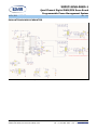
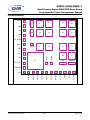
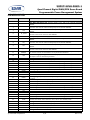
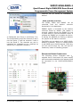
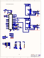
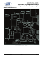
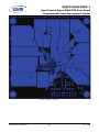
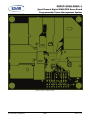
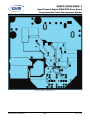
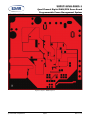
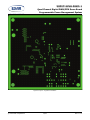
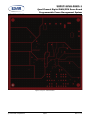
XRP9711EVB-DEMO-1
Quad Channel Digital PWM/PFM Demo Board
Programmable Power Management System
January 2014
Rev. 1.0.0
GENERAL DESCRIPTION
EVALUATION BOARD MANUAL
The XRP779711EVB-DEMO-1 board is a
complete, four channel power system. It
provides 1.5V, 1.2V 1.8V and 2.5V at
maximum currents of 10A, 10A, 6A and 6A
respectively. The 1.5V and 1.2V supplies can
be adjusted in 2.5mV increments, the 1.8V
and 2.5V supplies in 5mV increments. The
order and ramp rates for each supply can be
programmed to accommodate any sequencing
requirement. All power supply operations can
be controlled over an I2C interface. Faults,
output voltages and currents can also be
monitored. Two GPIO and three PSIO signals
are available and can be programmed to
provide a variety of functions. Unused
GPIO/PSIO pins can be programmed as I/O
expansion for a microcontroller. The board is
supported by PowerArchitectTM 5.1 and plugs
directly onto the interposer board acting as an
interface to Arduino controller.
FEATURES
XRP9711EVB-DEMO-1
• XRP9711 Programmable Power Module
o
Channels 1 and 2 driving external
power stages
o
Channel 3 and 4 internal converters
• 4 Channel Power System
• Wide Input Voltage Range: 5.5V-22V
• I2C Interface
− Programming
− Monitoring
− Control
• Arduino GPIO, PSIO and ENABLE
control
Exar Corporation
48720 Kato Road, Fremont CA 94538, USA
www.exar.com
Tel. +1 510 668-7000 – Fax. +1 510 668-7001
XRP9711EVB-DEMO-1
Quad Channel Digital PWM/PFM Demo Board
Programmable Power Management System
January 2014
Rev. 1.0.0
EVALUATION BOARD SCHEMATICS
Figure 1 XRP9711 Evaluation Board Schematics
Exar Corporation
48720 Kato Road, Fremont CA 94538, USA
www.exar.com
Tel. +1 510 668-7000 – Fax. +1 510 668-7001
XRP9711EVB-DEMO-1
Quad Channel Digital PWM/PFM Demo Board
Programmable Power Management System
GH2
2
LX2
3
4
GL_RTN2
5
BST1
6
24
30
31
LX3
LX3
35
AGND
PVIN
PVIN
32
33
PVIN
PVIN
36
37
38
AGND
LX4
PGND4
40
41
LX4
PVOUT4
44
LX4
45
PVOUT4
34
LDO5
7
ENABLE
11
42
43
17
18
19
20
21
22
23
PSIO0
10
SCL
GL_RTN1
SDA
39
GPIO1
9
GPIO0
8
PSIO2
GL1
PGND3
VOUT4
LX1
PVOUT3
28
PSIO1
GH1
27
VOUT3
GL2
26
25
29
1
LX3
BST2
PVOUT3
PIN ASSIGNMENT
14
15
16
VOUT2
13
VOUT1
12
AGND
VCC
AGND
AGND
Figure 2 XRP9711 Pin Assignment
© 2013 Exar Corporation
3/21
Rev. 1.0.0
XRP9711EVB-DEMO-1
Quad Channel Digital PWM/PFM Demo Board
Programmable Power Management System
PIN DESCRIPTION
Pin #
Name
Description
1
BST2
Boost pin. High side driver supply input.
2
GH2
High Side Gate Drive Out. Connect directly to the gate of an external N-channel
MOSFET.
3
LX2
Switch Node. Return for the high-side gate driver. Connect directly to the drain of the
lower FET. Also used to measure voltage drop across bottom MOSFETs
4
GL2
Low Side Gate Drive Out. Connect directly to the gate of an external N-channel
MOSFET.
5
GL_RTN2
6
BST1
Boost pin. High side driver supply input.
7
GH1
High Side Gate Drive Out. Connect directly to the gate of an external N-channel
MOSFET.
8
LX1
Switch Node. Return for the high-side gate driver. Connect directly to the drain of the
lower FET. Also used to measure voltage drop across bottom MOSFETs
9
GL1
Low Side Gate Drive Out. Connect directly to the gate of an external N-channel
MOSFET.
10
GL_RTN1
11
ENABLE
12
VCC
Low Side Gate Drive Return. This should be routed as a differential trace with GL.
Connect to the source of the low side MOSFET.
Low Side Gate Drive Return. This should be routed as a differential trace with GL.
Connect to the source of the low side MOSFET.
Enable. If ENABLE is pulled high or allowed to float high, the chip is powered up. The
pin must be held low for the XRP9711 to be placed into shutdown.
Controller Supply Voltage. Place a decoupling capacitor close to the controller IC.
This input is used in UVLO fault generation.
13
AGND
Analog Ground. This is the small signal ground connection.
14
AGND
Analog Ground. This is the small signal ground connection.
15
VOUT1
Feedback Pin. Connect to the output of the corresponding power stage
16
VOUT2
Feedback Pin. Connect to the output of the corresponding power stage
17
VOUT3
Feedback Pin. Connect to the output of the corresponding power stage
18
VOUT4
Feedback Pin. Connect to the output of the corresponding power stage
19
GPIO0
I/O Logic Signal. Can be configured as input or output.
20
GPIO1
I/O Logic Signal. Can be configured as input or output.
21
SDA
I2C Data. SMBus/I2C serial interface communication.
22
SCL
I2C Clock. SMBus/I2C serial interface communication.
23
PSIO0
24
PVOUT3
25
PVOUT3
Channel Output Power. Output voltage for the internal channel.
26
PGND3
Channel Output Ground. Output ground for the internal channel.
27
PVIN
28
PVIN
Channel Input Power. Internally connected to drain of upper switching MOSFET
29
LX3
Switch Node. Switch node of the internal channel.
30
LX3
Switch Node. Switch node of the internal channel.
31
LX3
Switch Node. Switch node of the internal channel.
32
PVIN
Channel Input Power. Internally connected to drain of upper switching MOSFET
33
PVIN
Channel Input Power. Internally connected to drain of upper switching MOSFET
34
LDO5
5V LDO Output. Used internally for power and may also be used for external power.
LDO that can remain active while the rest of the IC is in standby mode.
35
AGND
Analog Ground. This is the small signal ground connection.
36
AGND
Analog Ground. This is the small signal ground connection.
37
LX4
38
PGND4
Channel Output Ground. Output ground for the internal channel.
39
AGND
Analog Ground. This is the small signal ground connection.
© 2013 Exar Corporation
I/O Logic Signal, HV. Open drain, high voltage compliant. Can be configured as input
or output.
Channel Output Power. Output voltage for the internal channel.
Channel Input Power. Internally connected to drain of upper switching MOSFET
Switch Node. Switch node of the internal channel.
4/21
Rev. 1.0.0
XRP9711EVB-DEMO-1
Quad Channel Digital PWM/PFM Demo Board
Programmable Power Management System
Pin #
Name
40
LX4
41
PVOUT4
Description
Switch Node. Switch node of the internal channel.
Channel Output Power. Output voltage for the internal channel.
42
PSIO1
I/O Logic Signal, HV. Open drain, high voltage compliant. Can be configured as input
or output.
43
PSIO2
I/O Logic Signal, HV. Open drain, high voltage compliant. Can be configured as input
or output.
44
LX4
45
PVOUT4
Switch Node. Switch node of the internal channel.
Channel Output Power. Output voltage for the internal channel.
ORDERING INFORMATION
Refer to XRP9711’s datasheet and/or www.exar.com for exact and up to date ordering information.
© 2013 Exar Corporation
5/21
Rev. 1.0.0
XRP9711EVB-DEMO-1
Quad Channel Digital PWM/PFM Demo Board
Programmable Power Management System
USING THE EVALUATION BOARD
INPUT VOLTAGE RANGE
The input voltage range of XRP9711EVBDEMo-1 board is from 5.5V to 22V. The power
components have been optimized for a 12V
input rail. When running the board at an input
voltage other than 12V, use PowerArchitectTM
5.1
(PA5.1)
to
evaluate
the
system
performance.
I2C INTERFACE
The XRP9711 programmable power module
employs a standard I2C interface. Although the
I2C signals can be pulled up to LDO5 on board
by means of installing jumpers at the locations
JP1, JP2 and JP3, the I2C bus signals are
pulled up on the controller interface board by
default (refer to Appendix – jumpers installed
shorting pins 2 and 3 together at the locations
JP6 and JP7).
Load the PowerArchitectTM 5.1 software and
run it.
After selecting the proper family (Modules)
and the device (XRP9711), select the “Get
Started with the EVB-DEMO-1” option when
prompted as shown below.
OPERATING THE EVALUATION BOARD
The XRP9711EVB-DEMO-1 is designed to be
powered from either an AC/DC wall wart (the
output voltage must be in the range of 5.5V to
22V) connected to the barrel connector or a
test bench DC power supply (the voltage must
be in the range of 5.5V to 22V) connected to
the VIN connectors.
BRING UP PROCEDURE
Plug the XRP9711EVB-DEMO-1 evaluation
board to the controller interface board as
shown below.
When done, click “Create”. PA 5.1 will load the
default XRP9711EVB-DEMO-1 configuration
automatically.
Apply power to the board. Please refer to the
sections above on how to properly supply
power to the board and what voltage range to
use.
Turn on the Power supply.
Use USB cable to connect the computer (type
A) and the Arduino controller board (type B).
© 2013 Exar Corporation
6/21
Rev. 1.0.0
XRP9711EVB-DEMO-1
Quad Channel Digital PWM/PFM Demo Board
Programmable Power Management System
Go to the Tools tab in PA 5.1 and select
Boards.
The
software
will
identify
communication ports where it found the
Arduino controller board. Select the port.
Click the Flash button.
PA 5.1 is now communicating with the Arduino
controller board which is indicated in the lower
left corner.
PA 5.1 will go through the process of loading
configuration in the flash. Once it has
successfully completed the task, it will report
the outcome as seen above and reset the
device if “Automatically Reset After Flashing”
box checked (default option).
Close the window.
Programming the Configuration onto
XRP9711
Note that XRP9711EVB-DEMO-1 boards will be
pre-loaded with the default configuration.
To program a configuration go to the Tools tab
in PA 5.1 and select Program Flash.
Regulation
To enable channel regulation go to the Tools
tab in PA 5.1 and select Dashboard.
The program Flash window will appear.
© 2013 Exar Corporation
7/21
Rev. 1.0.0
XRP9711EVB-DEMO-1
Quad Channel Digital PWM/PFM Demo Board
Programmable Power Management System
Channels can be turned on individually if
desired.
GPIO and PISO interface
The GPIOs, PSIOs and ENABLE can be
controlled
from
the
Arduino
controller
dynamically in the dashboard.
ENABLE signal is connected to the Arduino
controller board by default (JP4 header is
shorted). Arduino drives the ENABLE pin low
to place XRP9711 into the shutdown mode. It
releases the ENABLE pin to enable the device.
If leaving the ENABLE pin floating is desired,
the jumper at JP4 shall be removed.
In Dashboard turn Group 1 and Group 2 on.
The configuration groups the channels 1 and 2
into the group 1, and the channels 3 and 4
into the group 2. The channels are now in
regulation as indicated by VOUT readings as
well as the in-regulation indicators.
The PSIOs are not pulled up on XRP9711EVBDEMO-1 by default. There is a loading option
to pull PSIOs up to LDO5 if desired. To do this,
one will need to short JP1, JP5, JP6 and JP7
headers by means of installing jumpers.
EVALUATION BOARD CONNECTIONS
The following picture illustrates how VIN
supplied from a test bench DC power supply
and instruments attached to the outputs would
be connected to the XRP9711EVB-DEMO-1
board.
© 2013 Exar Corporation
8/21
Rev. 1.0.0
2
3
4
5
6
1206
C32
35V
10uF
P0C3302 P0C3301
1206
C30
35V
10uF
P0C3202 P0C3201
1206
C13
50V
10UF
P0C3002 P0C3001
C12
50V
10UF
1210
P0C1202 P0C1201
EVALUATION BOARD SCHEMATICS
P0C1302 P0C1301
N0VIN
VIN
1210
1
P0T1200
C33
35V
10uF
T12
P0T1100
T11
A
A
SCL
C26
35V
10uF
1206
1206
C22
35V
10uF
P0C2602 P0C2601
1206
C7
50V
10UF
P0C2202 P0C2201
P0C701
1210
P0C702
P0C501
1210
0603
P0C3402 P0C3401
N0LDO5V
LDO5V
C5
50V
10UF
P0KB401
2
P0TP1302
0805
KB4
test point
Pad - Not Part
P0KB402
1
P0TP1301
C19
6.3V
330uF
1 P0TP901
P0C190N P0C1901
P0C1902
P0C190P
P0C180N P0C1801
P0C1802
P0C180P
1P0TP1001
2P0TP1002
1206
P0C3602 P0C3601
1206
P0C3802 P0C3801
1206
P0C3702 P0C3701
1206
P0C3902 P0C3901
P0R701
P0R702
C18 +
6.3V
330uF
N0VOUT10FB
VOUT1_FB
DNS
TP9
test point
PGND1
GND
KB6
Pad - Not Part
PCB Constraint: CH1 power ground meets EVB signal ground through vias at Cout
P0T200
C24
35V
10uF
T2
P0T100
T1
C34
DNS
C46
50V
0.01F
N0LDO5V
LDO5V
GND
N0GL2
GL2
R2
P0R201
P0R202
0603
0
TP7
test point
P0KB101
P0TP302
1
C4
6.3V
330uF
0805
C2
+
6.3V
330uF
P0C40N P0C401
P0C402
P0C40P
+
C21
10V
22uF
P0C20N P0C201
P0C202
P0C20P
C23
10V
22uF
1206
1206
P0C2902 P0C2901
0603
KB3
C29
C25
10V
22uF
VOUT2
1
DNS
P0TP701
test point
KB1
Pad - Not Part
P0KB102
N0VOUT4
VOUT4
C27
10V
22uF
P0C2102 P0C2101
VOUT4
FDML7610S
R4
DNS
P0C2302 P0C2301
PGND3
test point
1uH
1206
TP14
0805
N0VOUT30FB
VOUT3_FB
P0L202
1206
T4
P0R402
P0R401
P0L201
N0VOUT2
VOUT2
P0C2502 P0C2501
P0Q20MB1
P0TP301
0.6V to 1.8V 10A max rail
L2
KB2
2
TP3
N0LX2
LX2
P0Q20MB2
P0C2702 P0C2701
N0VOUT3
VOUT3
N0VOUT20FB
VOUT2_FB
DNS
DNS
TP1
test point
Pad - Not Part
N0VOUT40FB
VOUT4_FB
TP2
test point
PGND2
T14
0402
TP11
test point
Q2
P0Q201
P0Q202
P0Q203
P0Q204
Pad - Not Part
TP5
test point
C15
DNS
1
2
3
4
P0TP401
1
C35 +
50V
0.1UF
0
VOUT3
1P0TP201
C17
10V
47uF
P0R302
0603
1P0TP101
C16
10V
47uF
T13 P0T1300
test point
R3
P0R301
2P0TP102
T15
C6
DNS
GND
P0T1500
N0GH2
GH2
P0KB701
P0U1022
T10
2
SDA
N0LX4
LX4
P0T1000
2
P0U1037
37
LX4P0U1040
40
LX4P0U1044
44
LX4
P0U1041 41
PVOUT4
P0U1045 45
PVOUT4
P0U1038 38
PGND4
P0U1021
C41
DNS
P0T400
1210
1210
P0TP502
PSIO2
P0TP1102
22
C28 +
50V
0.1UF
P0U1043
13
14
35
36
39
N0SCL
SCL
T5
C9
10V
47uF
0603
21
C10
10V
47uF
P0T500
P0C3502 P0C3501
SDA
N0SDA
P0T300
1210
43
PSIO1
T3
P0C1702 P0C1701
N0PSIO2
PSIO2
P0U1042
+
C36
10V
22uF
DNS
N0VIN
VIN
TP4
50V
P0C1002 P0C1001
42
PSIO0
0402
T6
1210
N0PSIO1
PSIO1
P0U1023
N0LDO5V
LDO5V
0.01F
P0C4702 P0C4701
P0C1602 P0C1601
23
GPIO1
0402
N0PSIO0
PSIO0
P0U1020
N0LX3
LX3
P0T600
P0C4601 P0C4602
20
P0U1029
29
LX3P0U1030
30
LX3P0U1031
31
LX3
P0U1024 24
PVOUT3
P0U1025 25
PVOUT3
P0U1026 26
PGND3
AGND
AGND
P0U1035
AGND
P0U1036
AGND
P0U1039
AGND
N0GPIO1
GPIO1
C38
10V
22uF
1
P0TP1201
B
C47
GPIO0
C37
10V
22uF
TP12
5
P0U1019
P0U1014
P0T2100
19
P0U1013
T21
N0GPIO0
GPIO0
GL2
P0KB201
GL_RTN2
P0T2000
4
0805
GL2
P0KB202
VOUT4
N0GL2
P0KB301
P0U1018
P0U104
0805
LX2
P0T1400
P0KB302
VOUT3
P0U105
T20
N0LX2
LX2
P0C60N P0C60P
18
B
3
P0U103
C31
50V
0.1UF
1P0TP501
VOUT4_FB
N0VOUT40FB
N0GH2
GH2
1P0TP1101P0C150N P0C150P
P0U1017
2
P0U102
0603
17
GH2
P0C3102 P0C3101
N0VOUT30FB
VOUT3_FB
VOUT2
0603
P0U1016
N0BST2
BST2
P0C2802 P0C2801
16
BST2
P0C902 P0C901
VOUT1
N0VOUT20FB
VOUT2_FB
1
P0U101
P0U1015
P0C4101 P0C4102
XRP9711
15
C40
C39
10V
22uF
test point
10
P0C502
P0U1010
P0KB601
N0GL1
GL1
2
GL1
P0TP1402
ENABLE
GL_RTN1
N0VOUT10FB
VOUT1_FB
1
2
3
4
0805
9
P0U109
P0U1011
1uH
0603
0402
N0LX1
LX1
R7
DNS
P0L102
P0C4002 P0C4001
P0KB602
8
P0U108
P0L101
N0VOUT1
VOUT1
VOUT1
DNS
C14
50V
0.1UF
1
11
N0GH1
GH1
P0TP1401
LX1
N0ENABLE
ENABLE
7
2
GH1
L1
0.6V to 1.8V 10A max rail
TP10
test point
0603
12
LDO5V
KB5
Pad - Not Part
N0BST1
BST1
P0U107
P0U1034
P0KB501
T16
6
P0U106
BST1
P0R502
0
P0TP402
P0KB502
34
U1
XRP9711 Module
P0R501
0603
0603
0805
N0LDO5V
LDO5V
P0U102727
PVINP0U1028
28
PVINP0U1032
32
PVINP0U1033
33
PVIN
2
1
P0T1600
N05V
5V
VCC
GND
P0JP101
P0JP102
JP1
N0GL1
GL1
FDML7610S
R5
8P0Q108
7P0Q107
6P0Q106
5P0Q105
GND
P0U1012
0805
P0C2002 P0C2001
P0T900
C20
50V
1UF
TP13
N0LX1
LX1
P0Q10MB1
P0C2402 P0C2401
T9
C11
50V
10UF
8P0Q208
7P0Q207
6P0Q206
5P0Q205
C8
50V
10UF
GND
GND
P0C1102 P0C1101
0
Q1
P0Q101
P0Q102
P0Q103
P0Q104
P0Q10MB2
P0C1402 P0C1401
P0R102
P0R602
0
N0VIN0IC
VIN_IC
1210
P0R101
R6
P0R601
0603
P0T700
R1
1206
1210
P0C802
P0C801
N0VIN
VIN
N0GH1
GH1
T7
P0T800
T8
KB7
Pad - Not Part
P0KB702
PGND4
GND
PCB Constraint: CH2 power ground meets EVB signal ground through vias at Cout
GND
N0VOUT10FB
VOUT1_FB
N0VOUT20FB
VOUT2_FB
N0VOUT30FB
VOUT3_FB
D1
DNS
GND
GND
GND
0402
C43
16V
0.1UF
P0C4202 P0C4201
0402
C44
16V
0.1UF
P0C4302 P0C4301
0402
C45
16V
0.1UF
P0C4402 P0C4401
0402
1
3
P0P203
2
P0P202
P2
1P0TP601
C1
35V
120uF
N0VOUT40FB
VOUT4_FB
P0C4502 P0C4501
P0D102
P0TP802
2
test point
P0P201
2P0TP602
C3
35V
120uF
P0D101
P0C102 P0C101
N0VIN
VIN
P0C302 P0C301
C
P0TP801
1
TP8
C
C42
16V
0.1UF
GND
test point
GND
TP6
N05V
5V
N05V
5V
N05V
5V
T25
P0T2500
JP7
Header 2X10
N0PSIO0
PSIO0
JP6
P0T2400
JP3
P0R1301
0805
P0R1302
P0R801
1
P0R901
0603
P0R1001
0603
2 P0JP202
1 P0JP201
JP2
T24
P0T2300
N0PSIO2
PSIO2
2 P0JP302
1 P0JP301
JP5
N0PSIO1
PSIO1
GND
0603
2 P0JP502
1 P0JP501
R13
1.2K
P0DS101
GND
2 P0JP602
1 P0JP601
R8
4.7K
2
JP4
2 P0JP702
1 P0JP701
N0PSIO2
PSIO2
N0PSIO0
PSIO0
R9
4.7K
P0DS102
N0PSIO1
PSIO1
R10
4.7K
P0R802
N05V
5V
N0VIN
VIN
R11
4.7K
P0R902
2
1P0JP401
P0JP402
N0ENABLE
ENABLE
R12
4.7K
P0R1002
P0R1502
0603
0603
P0R1501
N0GPIO0
GPIO0
N0GPIO1
GPIO1
P0R1102
DNS
1 P0P101
3 P0P103
5 P0P105
7 P0P107
R14 DNS
9 P0P109 P0R14010805 P0R1402
11P0P1011
13P0P1013
15P0P1015
17P0P1017
19P0P1019
P0R1201
P0P104
0603
R15
N05V
5V
2
4
P0P106
6
P0P108
8
P0P1010
10
P0P1012
12
14
P0P1014
P0P1016
16
P0P1018
18
P0P1020
20
P0P102
P0R1202
N0SCL
SCL
N0SDA
SDA
P0R1101
P1
T23
T18
P0T2200
T22
T19
P0T1900
T17
GND
P0T1800
N0SDA
SDA
N0SCL
SCL
DS1
GND
P0T1700
GND
D
D
9/12
1
2
3
Title
XRP9711EVB-DEMO-1
EXAR
48720 Kato Road
Size: C
Rev: 1.0
Name:XRP9711EVB-DEMO-1.SchDoc
Fremont, CA 94538
Date: 12/18/2013
Time: 2:10:23 PM Sheet 1 of 1
www.exar.com
File: C:\SVN_LOCAL\XRP9711_temp_char_board\XRP9711EVB-DEMO-1\board\XRP9711EVB-DEMO-1.SchDoc
4
5
6
XRP9711EVB-DEMO-1
Quad Channel Digital PWM/PFM Demo Board
Programmable Power Management System
BILL OF MATERIAL
Ref.
Qty Manufacturer
Part Number
Size
Component
1
Exar Corporation
146-6703-01
3.15x3.05in
PCB
U1
1
Exar Corporation
XRP9711
12x12mm
LGA
Dual 6A Programmable
Power Module
Q1,Q2
2
Fairchild
FDML7610S
MLP 3x4.5
Dual N-Channel Power
Trench MOSFET
DS1
1
Wurth Elektronik
150120AS75000
1206
SMD Amber Chip LED
L1,L2
2
Cooper
Bussmann
DR127-1R0-R
12.5x12.5mm
Inductor 1µH, 3mΩ,
15.5A
C1,C3
2
Panasonic/Sanyo
35SVPF120M
F12
OSCON Capacitor
120µF, 35V
C2, C4, C18, C19
4
Panasonic/Sanyo
6TPF330M9L
7343 D3L
POSCAP Capacitor
330µF, 6.3V, 9mΩ
C5, C7, C8, C11, C12, C13
6
Murata
Corporation
GRM32ER71H106KA12L
1210
Ceramic Capacitor
10µF, 50V, X7R
C9, C10, C16, C17
4
Murata
Corporation
GRM32ER71A476KE15L
1210
Ceramic Capacitor
47µF, 10V, X7R
C14, C28, C31, C35
4
Murata
Corporation
GRM188R71H104KA93D
0603
Ceramic Capacitor
0.1µF, 50V, X7R
C20
1
Murata
Corporation
GRM21BR71H105KA12L
0805
Ceramic Capacitor 1µF,
50V, X7R
C21, C23, C25, C27, C36, C37,
C38, C39
8
Murata
Corporation
GRM31CR71A226KE15L
1206
Ceramic Capacitor
22µF, 10V, X7R
C22, C24, C26, C30, C32, C33
6
TDK Corporation C3216X7R1V106K160AC
1206
Ceramic Capacitor
10µF, 35V, X7R
C42, C43, C44, C45
4
Murata
Corporation
GRM155R71C104KA88D
0402
Ceramic Capacitor
0.1µF, 16V, X7R
C46, C47
2
Murata
Corporation
GRM155R71H103KA88D
0402
Ceramic Capacitor
0.01µF, 50V, X7R
R1
1
Vishay Dale
CRCW12060000Z0EAHP
1206
RES 0 Ω, 1/2W, SMD
R8, R9, R10, R11, R12
5
Panasonic
ERJ-3EKF4701V
0603
RES 4.7kΩ, 1/10W,
5%, SMD
R13
1
Panasonic
ERJ-6GEYJ122V
0805
RES 1.2kΩ, 1/8W, 5%,
SMD
JP1, JP2, JP3, JP4, JP5, JP6, JP7
7
Wurth Elektronik
61300211121
0.20x0.10in
Connector, Male
Header, 2 Positions,
100mil Spacing,
Vertical, TH
© 2013 Exar Corporation
10/21
Rev. 1.0.0
XRP9711EVB-DEMO-1
Quad Channel Digital PWM/PFM Demo Board
Programmable Power Management System
Ref.
Qty Manufacturer
Part Number
Size
Component
P1
1
Sullins
Connector
Solutions
SFH11-PBPC-D10-RABK
1.20x0.55in
Connector, Female
Header, 20 Positions,
100mil Spacing, RA, TH
P2
1
Switchcraft
RAPC722X
0.60x0.40in
Connector, Power Jack
Mini R/A, T/H
T1, T2, T3, T4, T5, T6, T10, T11,
T12, T13, T14, T15, T16, T17,
T18, T19, T20, T21
18 Wurth Elektronik
61300111121
0.10x0.10in
Square Test Posts, TH
TP1, TP3, TP4, TP5, TP6, TP8,
TP10, TP11, TP13, TP14
10 Wurth Elektronik
7471287
0.32x0.10in
Mounting Tabs
© 2013 Exar Corporation
11/21
Rev. 1.0.0
XRP9711EVB-DEMO-1
Quad Channel Digital PWM/PFM Demo Board
Programmable Power Management System
EVALUATION BOARD LAYOUT
Figure 3 Component Placement – Top Side
© 2013 Exar Corporation
12/21
Rev. 1.0.0
XRP9711EVB-DEMO-1
Quad Channel Digital PWM/PFM Demo Board
Programmable Power Management System
Figure 4 Layout – Top Layer
© 2013 Exar Corporation
13/21
Rev. 1.0.0
XRP9711EVB-DEMO-1
Quad Channel Digital PWM/PFM Demo Board
Programmable Power Management System
Figure 5 Layout – Bottom Layer
© 2013 Exar Corporation
14/21
Rev. 1.0.0
XRP9711EVB-DEMO-1
Quad Channel Digital PWM/PFM Demo Board
Programmable Power Management System
Figure 6 Layout – Middle Layer 1
© 2013 Exar Corporation
15/21
Rev. 1.0.0
XRP9711EVB-DEMO-1
Quad Channel Digital PWM/PFM Demo Board
Programmable Power Management System
Figure 7 Layout – Middle Layer 2
© 2013 Exar Corporation
16/21
Rev. 1.0.0
XRP9711EVB-DEMO-1
Quad Channel Digital PWM/PFM Demo Board
Programmable Power Management System
Figure 8 Layout – Signal Ground Plane
© 2013 Exar Corporation
17/21
Rev. 1.0.0
XRP9711EVB-DEMO-1
Quad Channel Digital PWM/PFM Demo Board
Programmable Power Management System
Figure 9 Layout – Internal Plane
© 2013 Exar Corporation
18/21
Rev. 1.0.0
1
2
3
4
5
6
Header 1X8 female H8.5mm
P0T100
P0T200
P0T300
P0T400
P0T500
P0T600
T26
N0ENABLE0L
ENABLE_L
P0R201
1
P0JP102
2
P0JP101
DNS
P0R1001
2
P0P104 4
P0P106
6
P0P108 8
P0P1010
10
P0P1012
12
P0P1014
14
P0P1016
16
P0P1018
18
P0P1020
20
P0P102
P0R1002
0805
JP3
GND
GND
N0+5V
+5V
R12
T20
T21
N0ENABLE
ENABLE
N0LDO5
LDO5
N0LDO3V3
LDO3V3
N0PSIO1
PSIO1
P0T2000
P0T2100
DNS
P0R1201
T22
P0T2200
P0R1202
0805
P_IOL1
P_AD1
P0T1200 T12
1P0P0AD101
P0T1400 T14
2P0P0AD102
P0T1600 T16
3P0P0AD103
P0P0AD104
4
5P0P0AD105
6P0P0AD106
B
R9
0
P0R901
N0I2C0POWER
I2C_POWER
P0R902
0805
P0T1800
T7
T10
T11
T13
T15
T17
P0T700
P0T1000
P0T1100
P0T1300
P0T1500
P0T1700
T18
P0T1900
Header 1X6 female H8.5mm
N0ENABLE
ENABLE
N0PSIO20UC
PSIO2_uC
N0PSIO10UC
PSIO1_uC
N0PSIO00UC
PSIO0_uC
N0GPIO1
GPIO1
N0GPIO0
GPIO0
N0TXD
TXD
N0RXD
RXD
N0GPIO0
GPIO0
N0GPIO1
GPIO1
P0P103
P0P105
R11
P0P107
N0VIN0BOARD
VIN_BOARD
P0P109
DNS
P0R1101
P0R1102
N0VIN
VIN
0805
P0P1011
P0P1013
N0PSIO2
PSIO2
N0PSIO0
PSIO0
P0P1015
P0P1017
P0P1019
8
P0P0IOL107
7
P0P0IOL106
6
P0P0IOL105
5
P0P0IOL104
4
P0P0IOL103
3
P0P0IOL102
2
P0P0IOL101
1
P0P0IOL108
T19
GND
GND
Header 1X8 female H8.5mm
B
T27
N0SDA
R14
DNS SDA
P0R1401
P0R1402
N0SCL
0805
DNS
SCL
P0R1502
R15
P0R1501
P0P101
Header 2X10 shrouded male
N0PSIO00UC
PSIO0_uC
R5
0
P0R501
P0R502
P0T2700
GND
1
3
5
7
9
11
13
15
17
19
2
1
0805
1
P0DS101
N0I2C0POWER
I2C_POWER
Header 1X10 female H8.5mm
GND
P0T2600
R10
SCL
N0SDA
SDA
JP2
P0JP201
T1
T2
T3
T4
T5
T6
DS1
P1
N0SCL
P0JP202
GND
DS2
1
P0JP302
2
GND
P0P0IOH1010
P0P0IOH109
A
JP1
P0JP301
N0RESET
RESET
N0+3V3
+3V3
N0+5V
+5V
N0PRGM0ERROR
PRGM_ERROR
2
1
P0P0POWER102
2
P0P0POWER103
3
P0P0POWER104
4
P0P0POWER105
5
P0P0POWER106
6
P0P0POWER107
7
P0P0POWER108
P0T900 T9
8
P0P0POWER101
10
9
P0P0IOH108
8
P0P0IOH107
7
P0P0IOH106
6
P0P0IOH105
5
P0P0IOH104
4
P0P0IOH103
3
P0P0IOH102
2
P0P0IOH101
1
P0R202
P0R301
SW1
P0R302
0805
SCL
N0SDA
SDA
N0AREF
AREF
APPENDIX - INTERFACE BOARD SCHEMATICS
R2
1.2K
P0DS102
P_POWER1
P_IOH1
N0SCL
1
4
P0SW102
C5
DNS
P0DS201
2
P0SW104
N0PRGM0DONE
PRGM_DONE
2
A
N0PRGM0INIT
PRGM_INIT
R3
1.2K
P0DS202
3
P0SW103
R4
4.7k
0805
0805
1
P0SW101
P0C502 P0C501 P0R402
P0R401
N0+5V
+5V
N0PSIO0
PSIO0
0805
N0PSIO10UC
PSIO1_uC
0805
R6
P0R601
0P0R602
N0PSIO1
PSIO1
0
N0PSIO2
PSIO2
N0PSIO20UC
PSIO2_uC
R1
P0R101
0805
P0R102
P0T2900
0805
P0T2800
T28
T29
T23
GND
P0JP702
P0T2300
P0C402 P0C401
P0C302 P0C301
C3
10V
22uF
C4
10V
22uF
CON5
JP5
N0SCL
SCL
GND
GND
N0SCL
SCL
N0SDA
SDA
1
3
P0CON505
5
P0CON507
7
P0CON509
9
P0CON501
P0CON503
N0ENABLE0L
ENABLE_L
GND
C
JP4
2 P0CON502
4 P0CON504
6 P0CON506
8 P0CON508
10 P0CON5010
2
P0JP401
1
T24
P0T2400
R7
4.7k
P0JP402
N0SDA
SDA
N0+5V
+5V
2
P0JP501
1
P0T2500
P0R702
R8
4.7k
P0R701
N0I2C0POWER
I2C_POWER
P0JP502
GND
N0+5V
+5V
0805
P0R801
T25
P0R802
C2
10V
22uF
P0JP701
P0JP602
P0JP601
0805
P0C202 P0C201
C
P0C102 P0C101
N0I2C0POWER
I2C_POWER
C1
10V
22uF
1
2
P0JP703
3
JP7
1
2
P0JP603
3
JP6
R13
N0VIN0L
VIN_L
DNS
P0R1301
P0R1302
N0VIN
VIN
0805
P0T800
T8
GND
N0SCL
SCL
1
P0P202 2
P0P203 3
P0P204 4
P0P201
N0SDA
SDA
D
D
P2
GND
19/21
Title:
XRP2ARDEVB-INT-1
Size:
B
Name: XRP2ARDUINO_Interface.SchDoc
Rev: 2.0
EXAR
48720 Kato Road
Fremont, CA 94538
www.exar.com
Date: 10/29/2013 Time: 12:07:02 PM
Sheet 1 of 1
File: J:\Apps_Simo\XRP2ARDEVB-INT-1\board\XRP2ARDUINO_Interface.SchDoc
1
2
3
4
5
6
XRP9711EVB-DEMO-1
Quad Channel Digital PWM/PFM Demo Board
Programmable Power Management System
BILL OF MATERIAL
Ref.
Qty
Manufacturer
Part Number
Size
Component
1
Exar Corporation
146-6703-01
4.40x2.10
PCB
DS1
1
Wurth Elektronik
150120RS75000
1206
SMD Red Chip LED
DS2
1
Wurth Elektronik
150120VS75000
1206
SMD Green Chip LED
C1, C2, C3, C4
4
Vishay Sprague
293D226X9010B2TE3
B
Tantalum Capacitor 22µF,
10V, 10%
R1, R5, R6, R9
4
Panasonic
ERJ-6GEY0R00V
0805
RES 0 Ω, 1/8W, 5% SMD
R2, R3
2
Panasonic
ERJ-6GEYJ122V
0805
RES 1.2kΩ, 1/8W, 5%, SMD
R4, R7, R8
3
Panasonic
ERJ-6GEYJ472V
0805
RES 4.7kΩ, 1/8W, 5%, SMD
SW1
1
Wurth Elektronik
430182050816
6x6mm
Tact Switch, SMD
CON5
1
Wurth Elektronik
61301021121
0.50x0.20in
Connector, Male Header, 10
Positions, Dual Row, 100mil
Spacing, Vertical, TH
JP1, JP2, JP3, JP4, JP5
5
Wurth Elektronik
61300211121
0.20x0.10in
Connector, Male Header, 2
Positions, 100mil Spacing,
Vertical, TH
JP6, JP7
2
Wurth Elektronik
61300311121
0.30x0.10in
Connector, Male Header, 3
Positions, 100mil Spacing,
Vertical, TH
P1
1
Wurth Elektronik
612020235221
1.20x0.55in
Connector, Male Header, 20
Positions, Dual Row, 100mil
Spacing, Shrouded, RA, TH
P2
1
Wurth Elektronik
653104124022
11x6mm
Wire-to-Board Connector,
Male, 4 Positions, 1.25mm
Spacing, Shrouded, SMT
P_IOH1
1
Wurth Elektronik
61301011121
1.00x0.10in
Connector, Male Header, 10
Positions, 100mil Spacing,
Vertical, TH
P_POWER1, P_IOL1
2
Wurth Elektronik
61300811121
0.80x0.10in
Connector, Male Header, 8
Positions, 100mil Spacing,
Vertical, TH
P_AD1
1
Wurth Elektronik
61300611121
0.60x0.10in
Connector, Male Header, 6
Positions, 100mil Spacing,
Vertical, TH
T23, T24, T25
3
Wurth Elektronik
61300111121
0.10x0.10in
Square Test Posts, TH
© 2013 Exar Corporation
20/21
Rev. 1.0.0
XRP9711EVB-DEMO-1
Quad Channel Digital PWM/PFM Demo Board
Programmable Power Management System
DOCUMENT REVISION HISTORY
Revision
Date
1.0.0
01/07/2014
Description
Initial release of document
BOARD REVISION HISTORY
Board Revision
Date
XRP9711EVBDEMO-1-01
12/20/13
Description
Initial release of evaluation board
FOR FURTHER ASSISTANCE
Email:
[email protected]
[email protected]
Exar Technical Documentation:
http://www.exar.com/TechDoc/default.aspx?
EXAR CORPORATION
HEADQUARTERS AND SALES OFFICES
48720 Kato Road
Fremont, CA 94538 – USA
Tel.: +1 (510) 668-7000
Fax: +1 (510) 668-7030
www.exar.com
NOTICE
EXAR Corporation reserves the right to make changes to the products contained in this publication in order to improve
design, performance or reliability. EXAR Corporation assumes no responsibility for the use of any circuits described herein,
conveys no license under any patent or other right, and makes no representation that the circuits are free of patent
infringement. Charts and schedules contained here in are only for illustration purposes and may vary depending upon a
user’s specific application. While the information in this publication has been carefully checked; no responsibility, however,
is assumed for inaccuracies.
EXAR Corporation does not recommend the use of any of its products in life support applications where the failure
malfunction of the product can reasonably be expected to cause failure of the life support system or to significantly affect
safety or effectiveness. Products are not authorized for use in such applications unless EXAR Corporation receives,
writing, assurances to its satisfaction that: (a) the risk of injury or damage has been minimized; (b) the user assumes
such risks; (c) potential liability of EXAR Corporation is adequately protected under the circumstances.
or
its
in
all
Reproduction, in part or whole, without the prior written consent of EXAR Corporation is prohibited.
© 2013 Exar Corporation
21/21
Rev. 1.0.0

![[LV2-KIT-MINI] 取扱・組立説明書](http://vs1.manualzilla.com/store/data/006570494_2-917345bb2fd6a7694b53bba6a9e032a0-150x150.png)