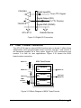
1
NuDAQ®
ACL-8112 Series
Enhanced Multi-Function
Data Acquisition Card
User’s Manual
Recycled Paper
©Copyright 2004 ADLINK TECHNOLOGY INC.
All Rights Reserved.
Manual Rev. 3.70: August 02, 2004
Part No.: 50-11012-202
The information in this document is subject to change without prior notice in
order to improve reliability, design, and function and does not represent a
commitment on the part of the manufacturer.
In no event will the manufacturer be liable for direct, indirect, special,
incidental, or consequential damages arising out of the use or inability to use
the product or documentation, even if advised of the possibility of such
damages.
This document contains proprietary information protected by copyright. All
rights are reserved. No part of this manual may be reproduced by any
mechanical, electronic, or other means in any form without prior written
permission of the manufacturer.
Trademarks
NuDAQ and ACL-8112 are registered trademarks of ADLINK TECHNOLOGY
INC.. Other product names mentioned herein are used for identification
purposes only and may be trademarks and/or registered trademarks of their
respective companies.
Getting Service from ADLINK
Customer Satisfaction is top priority for ADLINK TECHNOLOGY INC. If you
need any help or service, please contact us.
ADLINK TECHNOLOGY INC.
Web Site
http://www.adlinktech.com
Sales & Service
TEL
[email protected]
+886-2-82265877
Address
9F, No. 166, Jian Yi Road, Chungho City, Taipei, 235 Taiwan
FAX
+886-2-82265717
Please email or FAX your detailed information for prompt, satisfactory, and
consistent service.
Detailed Company Information
Company/Organization
Contact Person
E-mail Address
Address
Country
TEL
FAX
Web Site
Questions
Product Model
Environment
Detail Description
Suggestions for ADLINK
OS:
Computer Brand:
M/B:
Chipset:
Video Card:
NIC:
Other:
CPU:
BIOS:
Table of Contents
Chapter 1 Introduction ......................................................................1
1.1
1.2
1.3
1.4
Features ...............................................................................................3
Applications..........................................................................................4
Specifications .......................................................................................4
Software Support .................................................................................8
Chapter 2 Installation ........................................................................9
2.1
2.2
2.3
2.4
2.5
2.6
2.7
2.8
2.9
2.10
2.11
2.12
What You Have ....................................................................................9
Unpacking ..........................................................................................10
ACL-8112's Layout.............................................................................11
Jumper and DIP Switch Description...................................................13
Base Address Setting.........................................................................13
Analog Input Channel Configuration ..................................................15
DMA Channel Setting.........................................................................16
Internal/External Trigger Setting.........................................................17
Clock Source Setting..........................................................................18
IRQ Level Setting ...............................................................................18
D/A Reference Voltage Setting ..........................................................19
A/D Input Range Setting ....................................................................20
Chapter 3 Signal Connections .......................................................21
3.1
3.2
3.3
3.4
3.5
3.6
Connectors Pin Assignment ...............................................................21
Analog Input Signal Connection .........................................................24
Analog Output Signal Connection ......................................................26
Digital I/O Connection ........................................................................26
Timer / Counter Connection ...............................................................27
Daughter Board Connection...............................................................28
Chapter 4 Registers.........................................................................29
4.1
4.2
4.3
4.4
4.5
4.6
4.7
4.8
4.9
4.10
I/O Port Address.................................................................................30
A/D Data Registers ............................................................................31
A/D Channel Multiplexer Register ......................................................31
A/D Range Control Register...............................................................33
A/D Operation Mode Control Register................................................35
Interrupt Status Register ....................................................................36
Software Trigger Register ..................................................................36
Digital I/O register ..............................................................................37
D/A Output Register ...........................................................................38
Internal Timer/Counter Register .........................................................39
Table of Contents • i
Chapter 5 Operation Theory...........................................................41
5.1
5.2
5.3
5.4
A/D Conversion ..................................................................................41
D/A Conversion ..................................................................................44
Digital Input and Output .....................................................................44
Timer/Counter Operation ...................................................................45
Chapter 6 Calibration & Utilities ....................................................49
6.1
6.2
6.3
6.4
6.5
What you need ...................................................................................49
VR Assignment ..................................................................................50
D/A Adjustment ..................................................................................50
A/D Programmable Gain Amplifier adjustments .................................51
A/D Adjustment ..................................................................................51
Chapter 7 C Language Library .......................................................53
7.1
7.2
7.3
7.4
7.5
7.6
7.7
7.8
7.9
7.10
7.11
7.12
7.13
7.14
7.15
7.16
7.17
7.18
7.19
7.20
7.21
7.22
7.23
_8112_Initial.......................................................................................54
_8112_Switch_Card_No ....................................................................56
_8112_DI ...........................................................................................57
_8112_DI _Channel ...........................................................................58
_8112_DO..........................................................................................59
_8112_DA ..........................................................................................60
_8112_AD_Input_Mode .....................................................................61
_8112_AD_Set_Channel ...................................................................63
_8112_AD_Set_Range ......................................................................64
_8112_AD_Set_Mode........................................................................67
_8112_AD_Soft_Trig..........................................................................69
_8112_AD_Aquire..............................................................................70
_8112_CLR_IRQ................................................................................71
_8112_AD_DMA_Start.......................................................................72
_8112_AD_DMA_Status ....................................................................74
_8112_AD_DMA_Stop.......................................................................75
_8112_AD_INT_Start.........................................................................76
_8112_AD_INT_Status ......................................................................77
_8112_AD_INT_Stop .........................................................................78
_8112_AD_Timer ...............................................................................79
_8112_TIMER_Start ..........................................................................80
_8112_TIMER_Read .........................................................................81
_8112_TIMER_Stop...........................................................................81
Appendix A Demo Programs..........................................................83
Warranty Policy .....................................Error! Bookmark not defined.
ii • Table of Contents
How to Use This Guide
This manual is designed to help you use the ACL-8112. The manual
describes how to modify various settings on the ACL-8112 card to meet your
requirements. It is divided into seven chapters:
Chapter 1
Introduction
Gives an overview of the product features, applications, and
specifications.
Chapter 2
Installation
Describes how to install the ACL-8112. The layout of the ACL8112 is shown, the switch setting for base address, and jumper
setting for analog input channel configuration, reference
voltage setting, trigger source, interrupt level and DMA channel
are specified.
Chapter 3
Signal Connection
Describes the connectors' pin assignment and how to connect
the outside signal and devices with the ACL-8112.
Chapter 4
Registers
Describes the details of register format and structure of the
ACL-8112, this information is very important for programmers
who want to control the hardware by low-level programming.
Chapter 5
Operation Theory
Describes how to operate the ACL-8112. The A/D, D/A, DIO
and timer/counter functions are introduced. Also, some
programming concepts are specified.
Chapter 6
Calibration & Utility
Describes how to calibrate the ACL-8112 for accurate
measurement.
Chapter 7
C Language Library
Describes how to program the ACL-8112 by using the C
language library in DOS environment.
Appendix A
Demo Program
Describes some demonstration programs.
How to Use This Guide ● iii
1
Introduction
The ACL-8112 is a high performance, high speed multi-function data
acquisition card for IBM PC or compatible computers.
The ACL-8112 series is designed to combine all data acquisition functions,
such as A/D, D/A, DIO and timer/counter into a single board. The high-end
specifications of the card makes it ideal for a wide range of applications
requiring high speed. Figure 1.1 shows the block diagram of ACL-8112.
The ACL-8112 Series consists of three models, the ACL-8112HG, ACL8112DG and ACL-8112PG. The ACL-8112HG provides special high-gain
programmable instrument amplifier for low level input applications, such as
measurement of thermo-coupling signals. The ACL-8112DG provides high
speed sampling rates ( up to 100 KHz) at all gains ( x1, x2, x4, and x8) and
the ACL-8112PG provides 16 single-ended inputs with sampling up to 100
KHz with 5 levels of gain (x1, x2, x4, x8, x16)
All ACL-8112 Series feature 16 single-ended inputs or 8 differential inputs,
two12-bit double-buffered analog outputs, 16 digital inputs and 16 digital
outputs, and one timer/counter channel.
Introduction • 1
2 • Introduction
ANALOG
INPUT
REF 0 IN
CH 15
>
>
CH 1
CH 2
.
.
.
>
<
<
CH 0
REF 1 IN
GND
D/A 1 OUT
GND
D/A 0 OUT
MUX SCAN
CONTROL
16 channel
Single-ended
or
8 Differential
Analog
Multiplexer
+5V
GAIN
SELECT
DC/DC
CONVERTER
-15
AMP
+15
12-Bit
Code Latch
12-Bit
Code Latch
DMA SELECT
#1 OR #3
PC/AT BUS
DATA
BUFFER
DACK
DRQ
EXT.CLK
TO PACER TRIG
OUT 0
INTERRUPT
IRQ SELECT
TRIG
LOGIC
16 BIT
DIGITAL INPUT
REGISTER
16 BIT
DIGITAL INPUT
REGISTER
<
CONTROL
LOGIC
EOC
16 BIT
COUNTER #2
16 BIT
COUNTER #1
16 BIT
COUNTER #0
INTERNAL BUS
INPUT
BUFFER
12 Bit
A/D Converter
(B.B 774)
FR/2
2MHz
4 MHz
OSC.
Figure 1.1 ACL - 8112 BLOCK DIAGRAM
I/O PORT DECODER
D/A #1 12 BIT
MULITIPLYING D/A
D/A #0 12 BIT
MULITIPLYING D/A
EXTERNAL
TRIG
SOFTWARE
TRIG
PACER
TRIG
DO 15
.
.
D/O 0
DO
1
.
DI 15
.
.
.
DI 1
D/I 0
1.1
Features
The ACL-8112 series Enhanced Multi-function Data Acquisition Card
provides the following advanced features:
•
AT-Bus
•
16 single-ended or eight differential analog input channels for ACL8112DG/HG, 16 single-ended for ACL-8112PG
•
Bipolar or unipolar input signals for ACL-8112DG/HG, bipolar for ACL8112PG
•
Programmable gain
•
High gain for ACL-8112HG:( x0.5, x1, x5, x10, x50, x100, x500,
x1,000)
•
Normal gain for ACL-8112DG (x0.5, x1, x2, x4, x8)
•
Five Levels programmable gain for ACL-8112PG (x1, x2, x4, x8, x16),
x0.5 gain can be set by jumper
•
On-chip sample & hold
•
Two 12-bit monolithic multiplying analog output channels
•
16 digital output channels
•
16 digital input channels
•
Three programmable 16-bit down counters
•
Programmable sampling rate of up to 100KHz
•
Three A/D trigger modes: software trigger, programmable pacer
trigger, and external pulse trigger
•
AT interrupt IRQ capability: nine IRQ levels (IRQ3~IRQ15) are jumper
selectable
•
Integral DC-to-DC converter for stable analog power source
•
37-pin D-type connector
•
Compact size: half-size PCB
Introduction • 3
1.2
Applications
•
Industrial and laboratory ON/OFF control
•
Energy management
•
Annunciation
•
16 TTL/DTL compatible digital input channels
•
Security controller
•
Product test
•
Period and pulse width measurement
•
Event and frequency counting
•
Waveform and pulse generation
•
BCD interface driver
1.3
Specifications
♦ Analog Input (A/D)
•
Converter: ADS774 or equivalent, successive approximation type
•
Resolution: 12-bit
•
Number of channels:
ACL-8112DG/HG: 16 single-ended or eight differential
ACL-8112PG: 16 single-ended
•
Input Range: (Programmable)
•
ACL-8112HG:
Bipolar : ±10V, ± 5V, ±1V, ±500 mV, ±100mV, ±50mV, ±10mV, ±5mV
Unipolar: 0 to 10V, 0 to 1V, 0 to 0.1V, 0 to 0.01V
•
ACL-8112DG:
Bipolar : ±10V, ± 5V, ±2.5V, ±1.25V, ±0.625
Unipolar: 0 to 10V, 0 to 5V, 0 to 2.5V, 0 to 1.25V
4 • Introduction
•
ACL-8112PG:
Bipolar : ± 10V, ± 5V, ±2.5V, ±1.25V, ±0.625V
Or
Bipolar : ± 5V, ±2.5V, ±1.25V, ±0.625V, ±0.3125V
•
Conversion Time: 8µs
•
Overvoltage protection: Continuous ± 35V maximum
•
Accuracy:
(ACL-8112HG)
GAIN = 0.5, 1
GAIN = 5, 10
GAIN = 50, 100
GAIN = 500, 1000
0.01% of FSR ±1 LSB
0.02% of FSR ±1 LSB
0.04% of FSR ±1 LSB
0.04% of FSR ±1 LSB
(ACL-8112DG)
GAIN = 0.5, 1
GAIN = 2, 4
GAIN = 8
0.01% of FSR ±1 LSB
0.02% of FSR ±1 LSB
0.04% of FSR ±1 LSB
(ACL-8112PG)
GAIN = 0.5, 1, 2, 4
GAIN = 8, 16
0.015% of FSR ±1 LSB
0.02% of FSR ±1 LSB
•
Input Impedance: 10MΩ
•
AD conversion trigger modes: Software, Pacer, and External trigger
•
Data Transfer: Pooling, DMA, Interrupt
•
Sampling Rate:
•
100 KHz maximum for single channel
•
100 KHz maximum for multiplexing on ACL-8112PG
•
20 KHz maximum for multiplexing on ACL-8112DG/HG
Analog Output (D/A)
•
Converter: DAC7541 or equivalent, monolithic multiplying
•
Number of channels: Two double-buffered analog outputs
•
Resolution: 12-bit
Introduction • 5
•
Output Range:
Internal reference: (unipolar) 0 to 5V or 0 to 10V
External reference: (unipolar) max. +10V or -10V
•
Settling Time: 30µs
•
Linearity: ±1/2 bit LSB
•
Output driving capability: ±5mA max.
♦ Digital I/O (DIO)
•
Number of channels: 16 TTL compatible inputs and outputs
•
Input Voltage:
Low: Min. 0V; Max. 0.8V
High: Min. +2.0V
•
Input Load:
Low: +0.5V @ -0.2mA max.
High: +2.7V @+20mA max.
•
Output Voltage:
Low: Min. 0V; Max. 0.4V
High: Min. +2.4V
•
Driving Capacity:
Low: Max. +0.5V at 8.0mA (Sink)
High: Min. 2.7V at 0.4mA (Source)
♦ Programmable Counter
•
Device: 8254
•
A/D pacer: 32-bit timer (two 16-bit counter cascaded together) with a
2MHz time base
•
Pacer Output: 0.00046 Hz to 100 KHz
•
Counter: One 16-bit counter with internal 2MHz time base or external
clock source
6 • Introduction
♦ General Specifications
•
I/O Base Address: 16 consecutive address location
•
Interrupt IRQ: IRQ3, 5, 6, 7, 9, 10, 11, 12, 15 (nine levels)
•
DMA Channel: CH1 and CH3 (Jumper selectable)
•
Connector: 37-pin D-type connector
•
Operating Temperature: 0°C to 55°C
•
Storage Temperature: -20°C to 80°C
•
Humidity: 5 to 95%, non-condensing
•
Power Consumption:
ACL-8112DG/HG: +5 V @ 430 mA typical
+12V @ 150 mA typical
ACL-8112PG: +5 V @ 450 mA typical
12 V @ 150 mA typical
•
Dimension:
ACL-8112DG/HG: 162mm(L) x 115mm(W)
ACL-8112PG: 163 mm(L) x 123 mm(W)
Introduction • 7
1.4
Software Support
Programming Library
For users who are writing their own programs, we provide MS-DOS Borland
C/C++ programming library.
ACLS-DLL2 is the Development Kit for NuDAQ ISA-Bus Cards with Analog
I/O for windows 3.1/95(98)/NT. ACLS-DLL2 can be used in many
programming environments, such as VC++, VB, and Delphi. ACLS-DLL2 is
included in the ADLINK CD. To use this package a license is required.
LabView Driver
The ACLS-LVIEW includes the ACL-8112’s Vis, which is used to interface
with NI’s LabView software package. The ACLS-LVIEW supports Windows95(98)/NT. ACLS-LVIEW is included in the ADLINK CD. To use this package
a license is required.
8 • Introduction
2
Installation
This chapter describes how to install the ACL-8112 series products. Please
use the following steps to install the product.
•
Check what you have (section 2.1)
•
Unpacking (section 2.2)
•
Check the PCB and jumper location(section 2.3)
•
Install the hardware and setup the jumpers and switches (sections 2.4
to 2.12)
•
Cabling with external devices (section 2.13)
2.1
What You Have
In addition to this User's Manual, the package includes the following items:
•
ACL-8112 Enhanced Multi-function Data Acquisition Card
•
ADLINK CD
If any of these items are missing or damaged, contact ADLINK or the dealer
from whom the product was purchased. Save the shipping materials and
carton for future shipping or storage.
Note:
The utilities and libraries in the CD-ROM only support the ACL-8112
series under DOS environment. If you need to develop applications
under Windows 3.1, Windows 95 or Windows NT, please contact our
dealer for purchasing software development kit ACLS-DLL2.
Installation • 9
2.2
Unpacking
The card contains electro-static sensitive components that can be easily be
damaged by static electricity.
Therefore, the card should be handled on a grounded anti-static mat. The
operator should be wearing an anti-static wristband, grounded at the same
point as the anti-static mat.
Inspect the card module carton for obvious damage. Shipping and handling
may cause damage to the module. Ensure there is no shipping and handling
damage on the modules carton before continuing.
After opening the card module carton, extract the system module and place it
only on a grounded anti-static surface with component side up.
Again, inspect the module for damages. Press down on all the socketed IC's
to make sure that they are properly seated. Do this only with the module
place on a firm flat surface.
Note:
DO NOT ATTEMPT TO INSTALL A DAMAGED BOARD IN THE
COMPUTER.
You are now ready to install your card.
10 • Installation
. . . . . . . .
JP5
JP4
SW1
EXTTRG
INTTRG
3 5 6 7910111215NC
CN2
CN1
8112 Ver C.
JP8
8254
13 X
DRQ
13 X
DACK
JP7
EXTCLK
JP6
INTCLK
ADS774
VR1 VR2 VR3 VR4 VR5 VR6
-5V
-10V
CN3
JP3
INT
DIFF
SING
EXT1 EXT2
JP2
JP1
2.3
ACL-8112's Layout
. . . . . . . .
Figure 2.1-1 PCB Layout of the ACL-8112DG/HG Ver C.
Installation • 11
Figure 2.1-2 PCB Layout of the ACL-8112PG
12 • Installation
2.4
Jumper and DIP Switch Description
ACL8112's channels and base address can be changed by setting jumpers
and DIP switches on the card. The card's jumpers and switches are preset at
the factory. The jumper settings can be changed for the user’s applications.
A jumper switch is closed (sometimes referred to as "shorted") with the
plastic cap inserted over two pins of the jumper. A jumper is open when the
plastic cap is inserted over one or no pin(s) of the jumper.
2.5
Base Address Setting
The ACL-8112 requires 16 consecutive address locations in the I/O address
space. The base address of the ACL-8112 is restricted by the following
conditions.
1.
The base address must be within the range Hex 200 to Hex 3FF.
2.
The base address should not conflict with any PC reserved I/O
address. See Appendix A.
3.
The base address must not conflict with any add-on card on the
user’s PC. Please check your PC before installing the ACL-8112.
The ACL-8112's base address of registers is selected by a 6-positions DIP
switch SW1. The default setting of base address is set to be HEX 220. All
possible base address combinations are listed as Table 2.2. The base
address may be modified if the address HEX 220 has been occupied by
another add-on card.
SW1 : Base Address = Hex 220
DIP
ON
1
A ( 8
2
3
7
4
6
5
5
Figure 2.2 Default Base Address Setting
Installation • 13
I/O port
Address(Hex)
200-20F
210-21F
220-22F
(default)
230-23F
:
300-30F
:
3F0-3FF
A9
-(1)
-(1)
-(1)
-(1)
1
A8
ON
(0)
ON
(0)
ON
(0)
ON
(0)
2
A7
ON
(0)
ON
(0)
ON
(0)
ON
(0)
3
A6
ON
(0)
ON
(0)
ON
(0)
ON
(0)
4
A5
ON
(0)
ON
(0)
OFF
(1)
OFF
(1)
5
A4
ON
(0)
OFF
(1)
ON
(0)
OFF
(1)
-(1)
OFF
(1)
ON
(0)
ON
(0)
ON
(0)
ON
(0)
-(1)
OFF
(1)
OFF
(1)
OFF
(1)
OFF
(1)
OFF
(1)
Table 2.2 Possible Base Address Combinations
A0, ..., A9 corresponds to the PC Bus address lines
A9 is fixed at “1”.
How to define/determine the base address of the ACL-8112?
DIP1 to DIP5 of SW1 corresponds to the PC bus address line A8 to
A4 respectively. A9 is always 1 and A0 to A3 are always 0. If you want
to change the base address, you can only change the values of A8 to
A4 (the shadow area of the table below). The following table is an
example, of how to set a base address of Hex 220
Base Address: Hex 220
2
2
1
0
0
0
1
A9
A8
A7
A6
A5
14 • Installation
0
0
A4
0
A3
0
A2
0
A1
0
A0
2.6
Analog Input Channel Configuration
(This section applies to ACL-8112DG and ACL-8112HG only.)
The ACL-8112 offers 16 single-ended or eight differential analog input
channels. JP3 controls the analog input channel configuration. The setting of
JP3 is illustrated below:
SING
Single-ended
(default setting)
JP3
DIFF
SING
Differential Input
JP3
DIFF
Figure 2.3 Analog Input Channels Configuration
Installation • 15
2.7
DMA Channel Setting
The A/D data transfer of the ACL-8112 is designed with DMA transfer
capabilities. The setting of the DMA for channel 1 or channel 3 is controlled
by JP7 and JP8 on the ACL-8112DG/HG, and JP1 and JP2 on the ACL8112PG. Possible settings are shown below:
Note:
On floppy disk only machine, we suggest you set the DMA to level 3.
If you have a hard disk installed on the computer, level 1 is
preferable.
NO
DMA
DRQ
JP8/JP2
1 3 X
DACK
JP7/JP1
1 3 X
DMA 1
(Default)
DMA 3
Figure 2.4 DMA Channel Setting
16 • Installation
2.8
Internal/External Trigger Setting
The A/D conversion trigger source of the ACL-8112 can come from an
internal or external source. The internal or external trigger source is set by
JP4 on the ACL-8112DG/HG and by JP5 on the ACL-8112PG, as shown
on Figure 2.5. Note that there are two internal trigger sources, one is by
software trigger and the other is by the programmable pacer trigger, which
is controlled by the mode control register (see section 4.5).
JP4 / JP5
Internal Trigger
(default setting)
INTTRG
EXTTRG
JP4 / JP5
External Trigger
INTTRG
EXTTRG
Figure 2.5 Trigger Source Setting
JP6 / JP4
Internal Clock
Source : 2MHz
INTCLK
(default setting)
EXTCLK
JP6 / JP4
External Clock
Source
INTCLK
EXTCLK
Figure 2.6 Timer's Clock Source Setting
Installation • 17
2.9
Clock Source Setting
The 8254 programmable interval timer is used in the ACL-8112. It provides
three independent 16-bit programmable down counters. The input of
counter 2 is connected to a precision 2MHz oscillator which is the internal
pacer. The input of counter 1 is cascaded from the output of counter 2.
Channel 0 is free for user's applications. There are two selections for the
clock source of channel 0: the internal 2MHz clock or an external clock
signal from connector CN3 pin 37. The setting for the clock is shown in
Figure 2.6.
2.10 IRQ Level Setting
The ACL-8112 can connect to any one of the interrupt lines of the PC I/O
channel. The interrupt line is selected by JP5 of ACL-8112DG/HG or JP3 of
ACL-8112PG. If the user wishes to use the interrupt capability of ACL-8112,
select an interrupt level and place the jumper in the appropriate position to
enable the particular interrupt line.
The default interrupt level is IRQ15, which is selected by placing the jumper
on the pins in row number 15. Figure 2.7 shows the default interrupt jumper
setting IRQ15. The jumper can be removed from IRQ15 to other new pins to
change to another IRQ level.
Note:
Please note that no other add-on cards can share the same interrupt
level simultaneously.
JP5 / JP3
No Interrupt :
Interrupt level :
IRQ 3 5 6 7 9 10 11 12 15 X
JP5 / JP3
IRQ15
(default setting)
IRQ
3 5
6 7
9 10 11 12 15 X
Figure 2.7 IRQ Level Setting
18 • Installation
2.11 D/A Reference Voltage Setting
The D/A converter's reference voltage source can be internally or externally
generated. The external reference voltage is connected via CN3 pin 31
(ExtRef1) and pin 12 (ExtRef2), see section 3.1. The D/A reference source of
channel 1 and channel 2 are selected using JP2 for the ACL-8112DG/HG
and JP6 and JP7 for the ACL-8112PG respectively. Possible settings are
shown below:
JP2 or JP7 JP6
D/A CH1 is External
INTREF
INTREF
ExtRef1
ExtRef2
D/A CH2 is External
JP2 or JP7 JP6
D/A CH1 is External
D/A CH2 is Internal
INTREF
INTREF
ExtRef1
ExtRef2
JP2 or JP7 JP6
D/A CH1 is Internal
INTREF
INTREF
ExtRef1
ExtRef2
D/A CH2 is External
JP2 or JP7 JP6
D/A CH1 is Internal
D/A CH2 is Internal
INTREF
INTREF
ExtRef1
ExtRef2
Figure 2.8 D/A Voltage Setting
Installation • 19
The internal voltage can be set to -5V or -10V which is selected by JP1 for
the ACL-8112DG/HG and JP8 for the ACL-8112PG. Possible configurations
are specified in Figure 2.9. Note that the internal reference voltage is used
only when JP2 of the ACL-8112DG/HG or JP6 and JP7 of the ACL-8112PG
is set to internal reference.
Reference Voltage is
-5V (default setting)
Reference Voltage is
-10V
-10V
JP1 /
JP8
-5V
-10V
JP1 /
JP8
-5V
Figure 2.9 Internal Reference Voltage Setting
2.12 A/D Input Range Setting
(This section is for the ACL-8112PG only)
The A/D input range of the ACL-8112PG can be set to ±5V or ±10V using
JP9.
A/D Input Range is +/5V (default setting)
10
JP9
5
10
A/D Input Range is +/10V
JP9
5
20 • Installation
3
Signal Connections
This chapter describes the connectors of the ACL-8112. Signal connections
between the ACL-8112 and external devices, such as daughter boards or
other devices are also outlined.
3.1
Connectors Pin Assignment
The ACL-8112 comes equipped with two 20-pin insulation displacement
connectors - CN1 and CN2 and one 37-pin D-type connector - CN3. CN1 and
CN2 are located on the board and CN3 is located at the rear plate.
CN1 is used for digital output signals, CN2 is used for digital input signals
and CN3 is used for analog input, analog output and timer/counter's signals.
The pin assignment for each connector is illustrated in Figures 3.1 to 3.3.
•
CN2: Digital Signal Input (DI 0 to 15 )
CN2
DI 0
DI 2
DI 4
DI 6
DI 8
DI 10
DI 12
DI 14
GND
+5V
1
3
5
7
9
11
13
15
17
19
2
4
6
8
10
12
14
16
18
20
DI 1
DI 3
DI 5
DI 7
DI 9
DI 11
DI 13
DI 15
GND
+ 12V
Figure 3.1 Pin Assignment of CN2
Registers • 21
•
CN1: Digital Signal Output (DO 0 to 15 )
CN1
DO 0
DO 2
DO 4
DO 6
DO 8
DO 10
DO 12
DO 14
GND
+5V
1
3
5
7
9
11
13
15
17
19
2
4
6
8
10
12
14
16
18
20
DO 1
DO 3
DO 5
DO 7
DO 9
DO 11
DO 13
DO 15
GND
+12V
Figure 3.2 Pin Assignment of CN1
Note:
DO n:
DI n:
GND:
•
Digital output signal channel n
Digital input signal channel n
Digital ground
CN3: Analog Input/Output & Counter/Timer
(for single-ended connection: ACL-8112DG/HG/PG)
CN3
AI0
AI1
AI2
AI3
AI4
AI5
AI6
AI7
A.GND
A.GND
V.REF
ExtRef2
+12V
A.GND
D.GND
COUT0
ExtTrg
N/C
+5V
1
2
3
4
5
6
7
8
9
10
11
12
13
14
15
16
17
18
19
20
21
22
23
24
25
26
27
28
29
30
31
32
33
34
35
36
37
AI8
AI9
AI10
AI11
AI12
AI13
AI14
AI15
A.GND
A.GND
AO1
ExtRef1
AO2
GATE0
GATE
N/C
N/C
ExtCLK
Figure 3.3a Pin Assignment of CN3
22 • Registers
•
CN 3: Analog Input/Output & Counter/Timer
(for differential connection:: ACL-8112DG/HG)
CN3
AIH0
AIH1
AIH2
AIH3
AIH4
AIH5
AIH6
AIH7
A.GND
A.GND
V.REF
ExtRef2
+12V
A.GND
D.GND
COUT0
ExtTrg
N/C
+5V
1
2
3
4
5
6
7
8
9
10
11
12
13
14
15
16
17
18
19
20
21
22
23
24
25
26
27
28
29
30
31
32
33
34
35
36
37
AIL0
AIL1
AIL2
AIL3
AIL4
AIL5
AIL6
AIL7
A.GND
A.GND
AO1
ExtRef1
AO2
GATE0
GATE
N/C
N/C
ExtCLK
Figure 3.3b Pin Assignment of CN3
Note:
AIn:
AIHn:
AILn:
ExtRef n:
AOn:
ExtCLK:
ExtTrig:
CLK:
GATE:
COUT n:
V.ERF:
A.GND:
GND:
Analog Input Channel n (single-ended)
Analog High Input Channel n (differential)
Analog Low Input Channel n (differential)
External Reference Voltage for D/A CH n
Analog Output Channel n
External Clock Input
External Trigger Signal
Clock input for 8254
Gate input for 8254
Signal output of Counter n
Voltage Reference
Analog Ground
Ground
Registers • 23
3.2
Analog Input Signal Connection
The ACL-8112 provides 16 single-ended or eight differential analog input
channels. The analog signal can be converted to digital value by the A/D
converter. To avoid ground loops and obtain a more accurate measurement
of the A/D conversion, it is quite important to understand the signal source
type and how to choose the correct analog input mode: signal-ended or
differential. The ACL-8112 allows for the configuration through jumpers.
Single-ended Mode:
For single-ended mode, only one input is connected relative to ground and is
suitable for connecting with a floating signal source. Floating source means it
does not have any connection to ground. Figure 3.4 shows a single-ended
connection. Note that when two or more floating sources are connected, the
sources must be connected to common ground.
AIN
Floating
Signal
Source
Input Multipexer
Opertiona
Amplifie
To A/D Conver
V1
V2
n = 0, ..., 15
AGND
Figure 3.4 Floating source and single-ended
Differential input mode:
The differential input mode provides two inputs that respond to signal voltage
differences between them. If the signal source is ground-referenced, the
differential mode can be used to reduce ground loops. Figure 3.5 shows the
connection for differential input mode. However, even if the signal source is
locally grounded, the single-ended configuration can still be used when the
Vcm (Common Mode Voltage) is very small and the effect of ground loop is
negligible .
24 • Registers
n = 0, ..., 8
AIHn
Groun
Signal
Sourc
To A/D Converter
+
-
AILn
GND
Vcm = VG1 - VG2
VG1
VG2
Figure 3.5 Ground source and differential input
A differential mode must be used when the signal source is differential. A
differential source means the ends of the signal are not grounded. To avoid
dangerously high voltages between the local ground of the signal and the
ground of the PC system, a shorted ground path must be connected.
Figure 3.6 shows the connection for a differential source.
n = 0, ..., 8
To A/D Converter
AIHn
Differentia
Signal
Sourc
+
-
AILn
GND
Vcm = VG1 - VG2
VG1
VG2
Figure 3.6 Differential source and differential input
Registers • 25
If your signal sources contain both a floating and a local ground, the
differential mode should be used, with the floating signal source connected
as Figure 3.7.
n = 0, ..., 8
Floatin
Signal
Sourc
AIHn
High
AILn
Low
To A/D Converter
GND
Figure 3.7 Floating source and differential input
3.3
Analog Output Signal Connection
The ACL-8112 has two unipolar analog output channels. To make the D/A
output connections from the appropriate D/A output, please refer Figure 3.8.
-5 or -10
INT or Ext
Pin-30 ( AO0)
Ref In
Pin-32 ( AO1)
D/A Converter
+
To D/A Output
Pin-14 ( A.GND)
Analog GND
Figure 3.8 Connection of Analog Output Connection
3.4
Digital I/O Connection
The ACL-8112 provides 16 digital input and 16 digital output channels
through CN1 and CN2 onboard. The digital I/O signals are fully TTL/DTL
compatible. Details of the digital I/O signal specification can be referred to
in section 1.3.
26 • Registers
74LS244
Digital Input(DI)
From TTL Signal
Digital Output (DO)
To TTL Devices
74LS373
Digital GND (DGND)
Outside Device
ACL-8112
Figure 3.9 Digital I/O Connection
3.5
Timer / Counter Connection
The ACL-8112 has an interval 8254 timer/counter on board. It offers three
independent 16-bit programmable down counters; counter 1 and counter 2
are cascaded together as a timer pacer trigger for A/D conversions and
counter 0 is free for user applications. Figure 3.10 shows the 8254
timer/counter connection.
CN3 Pin-37
EXT
8254 Timer/Counter
INT
Counter 0
CLK0
GATE0
CN3 Pin-33
OUT0
CN3 Pin-16
OUT1
A/D Trigger
CN3 Pin-35
Vcc
Counter 1
CN3 Pin-34
2MHz
Oscillator
CLK1
GATE1
Counter 2
CLK2
GATE2
OUT2
Figure 3.10 Block Diagram of 8254 Timer/Counter
Registers • 27
The clock source of counter 0 can be internal or external, with the gate
being controlled externally and the output sent to CN3. As for counter 1
and counter 2, the clock source is internally fixed, while the gate can be
controlled externally and the output sent to CN3 too. All timer/counter
signals are TTL compatible.
3.6
Daughter Board Connection
The ACL-8112 can be connected with any of the five following daughter
boards, ACLD-8125, ACLD-9137, ACLD9182, ACLD9185, and ACLD9188.
The functionality and connections are specified below.
Connect with ACLD-8125
The ACLD-8125 has a 37-pin D-sub connector, which can be connected to
the ACL-8112HG through a 37-pin assemble cable. The most outstanding
feature of this daughter board is the CJC (cold junction compensation)
circuit on board. The thermo-coupler can be directly connected to the ACL8125 board.
Connect with ACLD-9137
The ACLD-9137 is a direct connector for the ACL-8112 card which is
equipped with a 37-pin D-sub connector. This board provides a simple way
for connecting simple applications that do not need complex signal
conditioning before an A/D conversion is performed.
Connect with ACLD-9182
The ACLD-9182 is a 16 channel isolated digital input board. This board is
connected to CN1 of the ACL-8112 via a 20-pin ribbon cable. The
advantage of this board is the 500Vdc isolation voltage that it provides,
thus it can protect your PC system from damage when an abnormal input
signal occurs.
Connect with ACLD-9185
The ACLD-9185 is a 16 channel SPDT relay output board. This board is
connected to CN2 of the ACL-8112 via a 20-pin ribbon cable. By using this
board, the external devices an be controlled through digital output signals.
Connect with ACLD-9188
The ACLD-9188 is a general purpose terminal board for all cards which
comes equipped with a 37-pin D-sub connector.
28 • Registers
4
Registers
A detailed description of the registers and its structure for the ACL-8112
are specified in this chapter. This information is useful for programmers
who wish to handle the card through low-level programming. Hence, a low
level programming syntax is also introduced. This information can also
assist beginners operate the ACL-8112 in the shortest possible time.
Registers • 29
4.1
I/O Port Address
The ACL-8112 requires 16 consecutive addresses in the PC I/O address
space. Table 4.1 shows the I/O address of each register with respect to the
base address. The function of each register is also listed.
I/O Address
Base + 0
Base + 1
Base + 2
Base + 3
Base + 4
Base + 5
Base + 6
Base + 7
Base + 8
Base + 9
Base + 10
Base + 11
Base + 12
Base + 13
Base + 14
Base + 15
Read
Counter 0
Counter 1
Counter 2
Not Used
A/D low byte
A/D high byte
DI low byte
DI high byte
Not Used
Not Used
Not Used
Not Used
Not Used
Not Used
Not Used
Not Used
Write
Counter 0
Counter 1
Counter 2
8254 Counter Control
CH1 D/A low byte
CH1 D/A high byte
CH2 D/A low byte
CH2 D/A high byte
Clear Interrupt Request
A/D Range Control
Channel MUX
Mode Control
Software A/D trigger
DO low byte
DO high byte
Not Used
Table 4.1 I/O Address
30 • Registers
4.2
A/D Data Registers
The ACL-8112 series has a 12-bit resolution for each analog input channel,
the digital data is store in the A/D data registers after an A/D conversion.
The A/D data is put into two 8 bits registers. The lowest byte data (8 LSBs)
are placed in address BASE+4 and the highest byte data (4 MSBs) are
placed in address BASE+5. A DRDY bit is used to indicate the status of the
A/D conversion. When the DRDY goes low, it means an A/D conversion is
complete.
Address : BASE + 4 and BASE + 5
Attribute: read only
Data Format:
Bit
BASE+4
BASE+5
7
AD7
0
6
AD6
0
5
AD5
0
4
AD4
DRDY
3
AD3
AD11
2
AD2
AD10
1
AD1
AD9
0
AD0
AD8
AD11 …. AD0: Analog to digital data. AD11 is the Most Significant
Bit(MSB). AD0 is the Least Significant Bit(LSB).
DRDY: Data Ready Signal.
1: A/D data is not ready
0: A/D conversion is completed.
It will be set to 1, when reading the low byte.
4.3
A/D Channel Multiplexer Register
This register is used to control the A/D channels. It's a write only register.
When a channel number is written to the register, the multiplexer switches
to another channel and waits until there’s a conversion and switches again.
Address : BASE + 10
Attribute: write only
Data Format:
Bit
BASE+10
7
X
6
X
5
CS1
4
CS0
3
CL3
2
CL2
1
CL1
0
CL0
CLn: multiplexer channel number (n=0~3).
CL3 is MSB, and CL0 is LSB.
CS0, CS1: Single-ended and Differential Selection (ACL-8112DG/HG only)
Registers • 31
CS0 and CS1 are used to determine which MPC508A chip is selected. The
MPC508A is used to multiplex between channels, when CS0 is set as 1,
the analog input channels from 0 to 7 are selectable, and when CS1 is set
to 1, channels 8 to 15 are selectable. When both CS0 and CS1 are set to 1,
it means the analog inputs are in differential mode. The possible analog
input channel selections combination is listed in the table below.
For ACL-8112PG, CS0 and CS1 is always set to zero, CL3~CL0 is used to
select the 16 single-ended channels.
Bit
Channel
S.E. CH0
S.E. CH1
S.E. CH2
S.E. CH3
S.E. CH4
S.E. CH5
S.E. CH6
S.E. CH7
S.E. CH8
S.E. CH9
S.E. CH10
S.E. CH11
S.E. CH12
S.E. CH13
S.E. CH14
S.E. CH15
D.I. CH0
D.I. CH1
D.I. CH2
D.I. CH3
D.I. CH4
D.I. CH5
D.I. CH6
D.I. CH7
7
X
X
X
X
X
X
X
X
X
X
X
X
X
X
X
X
X
X
X
X
X
X
X
X
X
6
X
X
X
X
X
X
X
X
X
X
X
X
X
X
X
X
X
X
X
X
X
X
X
X
X
5
CS1
0
0
0
0
0
0
0
0
1
1
1
1
1
1
1
1
1
1
1
1
1
1
1
1
S.E.: Single-ended Analog Input
D.I.: Differential Analog Input
32 • Registers
4
CS0
1
1
1
1
1
1
1
1
0
0
0
0
0
0
0
0
1
1
1
1
1
1
1
1
3
CL3
0
0
0
0
0
0
0
0
1
1
1
1
1
1
1
1
0
0
0
0
0
0
0
0
2
CL2
0
0
0
0
1
1
1
1
0
0
0
0
1
1
1
1
0
0
0
0
1
1
1
1
1
CL1
0
0
1
1
0
0
1
1
0
0
1
1
0
0
1
1
0
0
1
1
0
0
1
1
0
CL0
0
1
0
1
0
1
0
1
0
1
0
1
0
1
0
1
0
1
0
1
0
1
0
1
4.4
A/D Range Control Register
The A/D range register is used to adjust the analog input ranges for the
A/D channels. Two factor effects the input range: Gain and Polarity. For
ACL-8112PG, this register controls the PGA (programmable gain) directly
and there is no Unipolar setting. When a different gain value is set, the
analog input range is changed. For the ACL-8112DG/HG, both the PGA
and polarity are controlled by this register. Table 4.2 shows the relationship
between the register data and the A/D input range.
Address : BASE + 9
Attribute: write only
Data Format:
Bit
7
BASE+9
X
6
X
5
X
4
X
3
G3
2
G2
1
G1
0
G0
G0 to G3: Gain / Range selection, G3 is not used for ACL-8112PG
(This table is only for the ACL-8112HG: High Gain Card)
Bipolar
or
Input Range
G3 G2 G1 G0
GAIN
Unipolar
0
0
0
0
1
Bipolar
±5V
0
0
0
1
10
Bipolar
±0.5V
0
0
1
0
100
Bipolar
±0.05V
0
0
1
1
1,000
Bipolar
±0.005V
0
1
0
0
1
Unipolar
0V ~ 10V
0
1
0
1
10
Unipolar
0V ~ 1V
0
1
1
0
100
Unipolar
0V ~ 0.1V
0
1
1
1
1,000
Unipolar
0V ~ 0.01V
1
0
0
0
0.5
Bipolar
±10V
1
0
0
1
5
Bipolar
±1V
1
0
1
0
50
Bipolar
±0.1V
1
0
1
1
500
Bipolar
±0.01V
1
1
0
0
1
Unipolar
N/A
1
1
0
1
10
Unipolar
N/A
1
1
1
0
100
Unipolar
N/A
1
1
1
1
1,000
Unipolar
N/A
Table 4.2-1 Function of the Gain Control Bits
Registers • 33
(This table is only for the ACL-8112DG: Low Gain Card)
G3
G2
G1
G0
GAIN
1
0
0
0
0
0
0
0
0
0
0
0
0
0
1
1
1
1
0
0
0
1
1
0
0
1
1
0
0
1
0
1
0
1
0
1
0.5
1
2
4
8
1
2
4
8
Bipolar
or
Unipolar
Bipolar
Bipolar
Bipolar
Bipolar
Bipolar
Unipolar
Unipolar
Unipolar
Unipolar
Input Range
±10V
±5V
±2.5V
±1.25V
±0.625V
0V ~ 10V
0V ~ 5V
0V ~ 2.5V
0V ~ 1.25V
Table 4.2-2 Function of the Gain Control Bits
For the ACL-8112PG, the maximum range is changed by hardware jumper
configuration. JP9 is used to change the maximum analog input range form
±5V or ±10V. If JP9 is set as ±5V, the analog input range is listed as below.
G3
0
0
0
0
0
G2
0
0
0
0
1
G1
0
0
1
1
0
G0
0
1
0
1
0
GAIN
1
2
4
8
16
Analog Input Range
±5V
±2.5V
±1.25V
±0.625V
±0.3125V
Table 4.2-3 Analog Input Range ( max. is ±5V)
If JP9 is set as ±10V, the analog input range is listed as below
G3
0
0
0
0
0
G2
0
0
0
0
1
G1
0
0
1
1
0
G0
0
1
0
1
0
GAIN
1
2
4
8
16
Analog Input Range
±10V
±5V
±2.5V
±1.25V
±0.625V
Table 4.2-4 Analog Input Range (max. is ±10V)
34 • Registers
4.5
A/D Operation Mode Control Register
The A/D operation includes the analog signal conversion and the data
transformation. This register controls the internal trigger mode and data
transformation method. It is initialized by a software trigger or program polling
transfer when the PC is reset or powered on. The details of the A/D operation
are described in Chapter 5. There are four operation modes.
Address : BASE + 11
Attribute: write only
Data Format:
Bit
BASE+11
S2
0
0
0
1
S1
0
0
1
1
7
X
S0
0
1
0
0
6
X
5
X
4
X
3
X
2
S2
1
S1
0
S0
Operation Mode Description
Internal trigger is disable
software trigger and program polling (default)
timer pacer trigger and DMA transfer
timer pacer trigger and interrupt transfer.
Note:
1. When the system is powered on or reset, the A/D operation will be
initialized as "software trigger or program polling" mode.
2. No matter which mode is selected, the external trigger is available if JP4
is set as external trigger.
3. As long as the DMA mode is not used, the program polling mode is
always selectable. The synchronization of the A/D conversion and data
transfer should be of a concern when using program polling mode.
4. An interrupt will occur at the end of each conversion when the "timer
pacer trigger and interrupt transfer" mode is selected. If you want to use
the pacer trigger and interrupt transfer mode, you must enable the IRQ
level.
Registers • 35
4.6
Interrupt Status Register
The Interrupt Status Register is used to clear the interrupt status so a new
interrupt can be generated. If the ACL-8112 is in interrupt data transfer mode,
a hardware status flag will be set after each A/D conversion. You must clear
the status flag by writing any data to this register, so that the ACL-8112 can
generate a new or next interrupt if a new A/D conversion is to happen.
Address : BASE + 8
Attribute: write only
Data Format:
Bit
BASE+8
4.7
7
X
6
X
5
X
4
X
3
X
2
X
1
X
0
X
Software Trigger Register
If you want to generate a trigger pulse for the ACL-8112 to perform an A/D
conversion, you need to write data to this register, this will trigger the A/D
converter.
Address : BASE + 12
Attribute: write only
Data Format:
Bit
BASE+12
36 • Registers
7
X
6
X
5
X
4
X
3
X
2
X
1
X
0
X
4.8
Digital I/O register
There are 16 digital input channels and 16 digital output channels provided
by the ACL-8112. The address Base + 6 and Base + 7 are used for the digital
input channels, and the address Base + 13 and Base + 14 are used for digital
output channels.
Address : BASE + 6 & BASE + 7
Attribute: read only
Data Format:
Bit
Base + 6
Base + 7
7
DI7
DI15
6
DI6
DI14
5
DI5
DI13
4
DI4
DI12
3
DI3
DI11
2
DI2
DI10
1
DI1
DI9
0
DI0
DI8
7
6
5
4
3
2
DO7 DO6 DO5 DO4 DO3 DO2
DO15 DO14 DO13 DO12 DO11 DO10
1
DO1
DO9
0
DO0
DO8
Address : BASE + 13 & BASE + 14
Attribute: write only
Data Format:
Bit
Base + 13
Base + 14
Registers • 37
4.9
D/A Output Register
The D/A converter will convert the D/A output register data to an analog
signal. The register data at address Base + 4 and Base + 5 are used for D/A
channel 1 and Base +6 and Base +7 for D/A channel 2.
Address : BASE + 4 & BASE + 5
Attribute: write only
Data Format: (for D/A Channel 1)
Bit
Base + 4
Base + 5
7
DA7
X
6
DA6
X
5
DA5
X
4
DA4
X
3
2
DA3 DA2
DA11 DA10
1
DA1
DA9
0
DA0
DA8
Bit
7
6
5
4
3
2
Base + 6
DA7 DA6 DA5 DA4 DA3 DA2
Base + 7
X
X
X
X
DA11 DA10
DA0 is the LSB and DA11 is the MSB of the 12 bits data.
X: does not matter
1
DA1
DA9
0
DA0
DA8
Address : BASE + 6 & BASE + 7
Attribute: write only
Data Format: (for D/A Channel 2)
Note: The D/A registers are "double buffered" so that the D/A analog output
signals will not updated until the second (high) byte contains data or
written to. This will ensure a single step transition for a D/A conversion.
38 • Registers
4.10 Internal Timer/Counter Register
Two 8254 counters are used for periodical triggering of the A/D converter,
with one left for user applications. The 8254 occupies four I/O address
locations in the ACL-8112 as listed below. Users may refer to NEC's or Intel's
data sheet for full detail of the 8254. A summary of the information is
specified in Appendix B.
Address : BASE + 0 ~ BASE + 3
Attribute: read / write
Data Format:
Base + 0
Base + 1
Base + 2
Base + 3
Counter 0 Register ( R/W)
Counter 1 Register ( R/W)
Counter 2 Register ( R/W)
8254 CONTROL BYTE
Registers • 39
5
Operation Theory
The operation theory of the ACL-8112 card is described in this chapter. The
function description includes the A/D conversion, D/A conversion, digital I/O
and counter/timer. The operation theory can assist the user understand how
to manipulate or program the ACL-8112.
5.1
A/D Conversion
Before programming the ACL-8112 to perform an A/D conversion, you need
to understand the following issues:
•
A/D conversion procedure
•
A/D trigger mode
•
A/D data transfer mode
•
Signal Connection
A/D Conversion Procedure
An A/D conversion is initiated when a trigger source is triggered, the A/D
converter will start to convert the signal to a digital value. The ACL-8112
provides three trigger modes as discussed below.
During an A/D conversion, the DRDY bit of the A/D data register is cleared to
indicate the data is not ready. After a conversion is completed, the DRDY bit
will return a low (0) signal. This indicates users now can read the converted
data from the A/D data registers. Please refer to section 4.2 for the A/D data
format.
Operation Theory • 41
The A/D data should now be transferred into the PC's memory for further
processing. The ACL-8112 provides three data transfer modes that allow
users to optimize their DAS system. Refer to section 5.1.3 for data transfer
modes.
A/D Trigger Modes
The ACL-8112’s A/D conversion can be triggered by either an Internal or
External trigger source. JP5 is used to set either internal or external triggers.
Please refer to section 2.8 for details. Whenever an external source is set,
the internal sources are disabled.
The two internal sources can either be software or timer pacer triggered
which is controlled by the A/D operation mode control register (BASE+11). In
total there are three different trigger sources available to the ACL-8112. The
trigger conditions are described below:
Software trigger
This trigger source is software controllable. That is, the A/D conversion is
initiated when any value is written into the software trigger register
(BASE+12). This trigger mode is suitable for low speed A/D conversions.
Under this mode, the timing of the A/D conversion is fully controlled by the
software. However, it is difficult to have total control over a fixed A/D
conversion rate unless another timer interrupt service routine is used to
generate a fixed trigger rate.
Timer Pacer Trigger
An onboard 8254 timer/counter chip is used to provide a trigger source for
the A/D conversion at a fixed rate. Two counters are cascaded together to
generate a trigger pulse at precise intervals. Refer to section 5.4 for details of
the 8254 architecture. This mode is ideal for high speed A/D conversions. It
can be combined with DMA or interrupt data transfer. It is recommended that
this mode be used for applications that require a fixed and precise A/D
sampling rate.
External Trigger
Through pin-17 of CN3 (ExtTrig), the A/D conversion can also be performed
when a rising edge from an external source occurs. The conversion rate of
this mode is more flexible than the previous two modes, because users can
easily control an external device. An external trigger can be combine with
DMA transfer, interrupt data transfer, or even program polling data transfer.
Generally, the interrupt data transfer is used when external trigger mode is
used.
42 • Operation Theory
A/D Data Transfer Modes
On the ACL-8112, there are three A/D data transfer modes that can be used
when A/D conversion is completed. The data transfer mode is controlled by
the mode control register (BASE+11). The transfer modes are described
below:
Software Data Transfer
Usually, this mode is used with software A/D trigger mode. After the A/D
conversion is triggered by the software, the software will poll the DRDY bit
until it becomes high. Whenever the low byte of the A/D data is read, the
DRDY bit will be cleared to indicate the data has been read.
It is possible to read the A/D converted data without polling. The A/D
conversion time will not excess 8µs on the ACL-8112 card. Hence, after a
software trigger, the software can wait for at least 8µs then read the A/D
register without polling.
Interrupt Transfer
The ACL-8112 provides hardware interrupt capability. Under this mode, an
interrupt signal is generated when an A/D conversion has ended and the data
is ready to be read. It is useful to combine the interrupt transfer mode with
the timer pacer trigger mode. Under this combination, the data transfer is
essentially asynchronous with the controlling software.
When the interrupt transfer mode is used, you have to set the interrupt IRQ
level using hardware jumpers. Refer to section 2.10 for IRQ jumper setting.
After an A/D conversion is completed, a hardware interrupt will be inserted
and its corresponding ISR (Interrupt Service Routine) will be invoked and
executed. The converted data is transferred by the ISR program.
DMA Transfer
The DMA (Direct Memory Access) allows data to be transferred directly
between the ACL-8112 and the PC memory at the fastest possible rate,
without using any CPU time. The A/D data is automatically transferred to
PC's memory after conversion is completed.
The DMA transfer mode is very complex to program. It is recommended that
a high level programming library be used to operate this card in this mode. If
you wish to program a software which can handle DMA data transfer, refer to
information about the 8237 DMA controller.
Operation Theory • 43
5.2
D/A Conversion
The operation of the D/A conversion is simpler than the A/D operation. You
only need to write the digital values into the D/A data registers and the
corresponding voltage will be outputted through AO1 or AO2. Refer to
section 4.9 for information about the D/A data registers. The mathematical
relationship between the digital number DAn and the output voltage is
formulated as follows:
Vout = −Vref ×
DAn
4096
where Vref is the reference voltage, Vout is the output voltage, and DAn is
the digital value in the D/A data registers.
Before performing the D/A conversion, users should be aware of the D/A
reference voltage which is set by JP1, JP2 and JP3. Please refer to section
2.11 for jumper setting. The reference voltage will effect the output voltage. If
the reference voltage is -5V, the D/A output scaling will be from 0 to 5V. If the
reference voltage is -10V, the D/A output scaling will be 0 to 10V.
Note that the D/A registers are "double buffered" so that the D/A analog
output signals will not be updated until the high byte is written. When writing
12-bit data to the D/A registers, the low byte must be written to first before
the high byte. This procedure will ensure a single step transition for a D/A
conversion.
5.3
Digital Input and Output
To program the digital I/O operation is fairly straight forward. The digital input
operation just reads data from its corresponding registers, and the digital
output operation just writes data to its corresponding registers. The digital I/O
registers are shown in section 4.9. Note that the DIO data channel can only
be read or written in forms of 8-bits. It is impossible to access individual bits.
44 • Operation Theory
5.4
Timer/Counter Operation
The ACL-8112 has an 8254 interval timer/counter onboard. Refer to section
3.5 for signal connection and the configuration of the counter.
The 8254 Timer / Counter Chip
The Intel (NEC) 8254 contains three independent, programmable, multimode 16 bit counter/timers. The three independent 16 bit counters can be
clocked at rates from DC to 5MHz. Each counter can be individually
programmed with six different operating modes by appropriately formatted
control words. The most commonly uses for the 8254 in microprocessor
based systems are:
•
programmable baud rate generator
•
event counter
•
binary rate multiplier
•
real-time clock
•
digital one-shot
•
motor control
For more information about the 8254, please refer to the NEC
Microprocessors and peripherals or Intel Microsystems Components
Handbook.
Pacer Trigger Source
Counter 1 and 2 are cascaded together to generate a timer pacer trigger for
the A/D conversion. The frequency of the pacer trigger is software
controllable. The maximum pacer signal rate is 2MHz/4=500K which exceeds
the maximum A/D conversion rate of the ACL-8112. The minimum signal rate
is 2MHz/65535/65535, which is a very slow frequency that user may never
use.
General Purpose Timer/ Counter
Counter 0 is free for user applications. The clock source, gate control signal
and the output signal are sent via CN3. The general purpose timer/counter
can be used as an event counter, used for measuring frequency or other
functions. Please refer to 'Timer/Counter Applications' section for examples.
Operation Theory • 45
I/O Address
The 8254 in the ACL-8112 occupies four I/O address as shown below.
BASE + 0
BASE + 1
BASE + 2
BASE + 3
LSB OR MSB OF COUNTER 0
LSB OR MSB OF COUNTER 1
LSB OR MSB OF COUNTER 2
CONTROL BYTE
The programming of the 8254 is control by registers BASE+0 to BASE+3.
The function of each register is specified in this section. For more detailed
information, refer to the 8254 handbook.
Control Byte
Before loading or reading any of these individual counters, the control byte
(BASE+3) must be loaded first. The format of the control byte is:
Bit
7
6
5
4
3
2
1
0
SC1
SC0
RL1
RL0
M2
M1
M0
BCD
SC1 & SC0 - Select Counter ( Bit7 & Bit 6)
SC1
0
0
1
1
SC0
0
1
0
1
COUNTER
Select Counter 0
Select Counter 1
Select Counter 2
ILLEGAL
RL1 & RL0 - Select Read/Load operation ( Bit 5 & Bit 4)
RL1
0
0
1
1
RL0
0
1
0
1
46 • Operation Theory
OPERATION
COUNTER LATCH FOR STABLE READ
READ/LOAD LSB ONLY
READ/LOAD MSB ONLY
READ/LOAD LSB FIRST, THEN MSB
M2, M1 & M0 - Select Operating Mode ( Bit 3, Bit 2, & Bit 1)
M2
0
0
x
x
1
1
M1
0
0
1
1
0
0
M0
0
1
0
1
0
1
MODE
0
1
2
3
4
5
BCD - Select Binary/BCD Counting ( Bit 0)
0
16-BITS BINARY COUNTER
1
BINARY CODED DECIMAL (BCD) COUNTER (4
DIGITAL)
Note: The count of the binary counter is from 0 up to 65,535 and the count
of the BCD counter is from 0 up to 9,999
Mode Definitions
With the 8254, six operating modes can be selected:
•
Mode 0: Interrupt on Terminal Count
•
Mode 1: Programmable One-Shot.
•
Mode 2: Rate Generator
•
Mode 3: Square Wave Rate Generator
•
Mode 4: Software Triggered Strobe
•
Mode 5: Hardware Triggered Strobe
Detail description of these six modes can be found in the Intel Microsystems
Components Handbook Volume II Peripherals.
Operation Theory • 47
6
Calibration & Utilities
With data acquisition processes, knowing how to calibrate your
measurement devices to maintain its accuracy is of high importance. Users
can calibrate the analog input and analog output channels under user’s
operating environment to optimize the accuracy of the equipment. This
chapter will guide you through calibrating the ACL-8112.
6.1
What you need
Equipment required for the calibration of the ACL-8112 card:
•
Calibration program: The calibration program 8112util.exe. Once the
program is executed, it will guide you through the calibration
process. This program is included in the delivered package.
•
A 5 1/2 digit multimeter (6 1/2 is recommended)
•
A voltage calibrator or a very stable and noise free DC voltage
generator.
Calibration & Utilities • 49
6.2
VR Assignment
There are six variable resistors (VR) on the ACL-8112DG/HG board.
These allow the user to make adjustments to the A/D and D/A channels.
The function of each VR is specified as Table 6.1-1.
VR1
VR2
VR3
VR4
VR5
VR6
A/D full scale adjustment
A/D bipolar offset adjustment
D/A channel 1 full scale adjustment
D/A channel 2 full scale adjustment
A/D programmable amplifier offset adjustment
A/D unipolar offset adjustment
Table 6.1-1 Function of VRs in ACL-8112DG/HG
There are five variable resistors (VR) on the ACL-8112PG board. These
allow the user to make adjustment to the A/D and D/A channels. The
function of each VR is specified as Table 6.1-2.
VR1
VR2
VR3
VR4
VR5
A/D full scale adjustment
A/D offset adjustment
D/A channel 1 full scale adjustment
D/A channel 2 full scale adjustment
A/D programmable amplifier offset adjustment
Table 6.1-2 Function of VRs in ACL-8112PG
6.3
D/A Adjustment
D/A CH1 calibration
1.
Connect the DVM <+> to CN3.AO1<PIN 30>, and the VDM<-> to
CN3.GND <PIN 10>.
2.
Write a digital value into the D/A register (BASE+4 and BASE+5).
3.
Trim VR3 until +5 V appears on the DVM.
50 • Calibration & Utilities
D/A CH2 calibration
6.4
1.
Connect the DVM <+> to CN3.AO2<PIN 32>, and the DVM<-> to
CN3.GND <PIN 10>.
2.
Write a digital value into the D/A register (BASE+6 and BASE+7).
3.
Trim VR4 until +5 V appears on the DVM.
A/D Programmable Gain Amplifier adjustments
This setup is to reduce the PGA offset voltage.
1.
Connect CN3.AI0 <PIN 2> to CN3.GND <PIN 9>
2.
Trim VR5 until the reading displayed on the monitor of the
8112UTIL.exe software is approximately 0 and below 0.50.
6.5
A/D Adjustment
Bipolar Calibration
1.
Adjust the voltage calibrator’s voltage output to –4.9987V. Connect
the voltage calibrator’s <+> to CN3.AI0 <PIN 1> and the voltage
calibrator’s<-> to CN3.AGND<PIN 9>.
2.
Trim VR2 to obtain a reading that toggles between 0 and 1. This
value is displayed on the monitor of the calibration program
8112UTIL.exe. Then proceed to the next step.
3.
Adjust the voltage calibrator’s voltage output to +4.9963V. Connect
the voltage calibrator’s <+> to CN3.AI0 <PIN 1> and the voltage
calibrator’s <-> to CN3.AGND<PIN 9>.
4.
Trim VR1 to obtain a reading that toggles between 4094 and 4095.
This value is displayed on the monitor of the calibration program
8112UTIL.exe.
Calibration & Utilities • 51
Unipolar Calibration(Only for ACL-8112DG/HG)
1.
Adjust the voltage calibrator’s voltage output to –4.9987V. Connect
the voltage calibrator’s <+> to CN3.AI0 <PIN 1> and the voltage
calibrator’s<-> to CN3.AGND<PIN 9>.
2.
Trim VR2 to obtain a reading that toggles between 0 and 1. This
value is displayed on the monitor of the calibration program
8112UTIL.exe. Then proceed to the next step.
3.
Adjust the voltage calibrator’s voltage output to +1.22mV. Connect
the voltage calibrator’s <+> to CN3.AI0 <PIN 1> and the voltage
calibrator’s<-> to CN3.AGND<PIN 9>.
4.
Trim VR6 to obtain a reading that toggles between 0 and 1. This
value is displayed on the monitor of the calibration program
8112UTIL.exe. Then proceed to the next step
5.
Adjust the voltage calibrator’s voltage output to +9.9963V. Connect
the voltage calibrator’s <+> to CN3.AI0 <PIN 1> and the voltage
calibrator’s<-> to CN3.AGND<PIN 9>
6.
Trim VR1 to obtain a reading that toggles between 4094 and 4095.
This value is displayed on the monitor of the calibration program
8112UTIL.exe.
A calibration utility software diskette is included in the product package.
Detail calibration procedures and description can be found in the utility.
Users need to execute the calibration utility and follow the procedures
carefully to obtain best results and accurate measurements.
52 • Calibration & Utilities
7
C Language Library
There are 23 call functions available in the C programming Library, all
functions associated with the ACL-8112 are covered, it includes A/D
conversions, D/A conversions, Digital Inputs and Outputs, etc.
Much of the programming time is saved under the C Language library. The
library also covers support for data collection on the interrupt or DMA from
the internal time clock for A/D conversions. Note that the DMA data transfer
processes only on a fixed A/D channel.
Example programs are also included in this disk, this will help fast track users
to understand the library. A detailed description of each function in the library
is discussed in the following sections.
Note that each function name uses the following conventions:
_8112XX_function(). Where XX is substituted for the particular 8112 model.
For example ACL-8112DG, ACL-8112HG and ACL-8112PG.
C Language Library • 53
7.1
_8112_Initial
Description
All ACL-8112 cards are initialized according to its card number and its
corresponding base address. Every ACL-8112 Multi-Function Data
Acquisition Card must be initialized using this function before any other
function calls are permitted.
Syntax
int _8112_Initial(int card_number, int type, int
base_addresss )
int _8112pg_Initial(int card_number, int
base_addresss )
Argument:
card_number: the card number to be initialized, only
two
cards can be initialized, the card
number must be CARD_1 or CARD_2.
Type
:there are 4 different types of ACL-8112
cards, they are:
A8112B_HG: 8112 High Gain card Ver. B
A8112B_DG: 8112 Low Gain card Ver. B
A8112C_HG: 8112 High Gain card Ver. C
A8112C_DG: 8112 Low Gain card Ver. C
Note: the difference between Ver.B and
Ver.C is the Multi-Scan Register. The
control code for each version is
slight different. For details, please
refer to the hardware manual for the
specific ACL-8112 card.
base_address: the I/O port base address of the card
is set at 220 Hex default.
Return Code:
ERR_NoError
ERR_InvalidBoardNumber
ERR_BaseAddressError
54 • C Language Library
Example:
#include
"8112.h"
main()
{
int ErrCode;
Errcode = _8112_Initial( CARD_1, A8112B_HG, 0x210 );
if ( ErrCode != ERR_NoError )
exit(0);
ErrCode = _8112_Initial( CARD_2, A8112B_DG, 0x220 );
if ( ErrCode != ERR_NoError )
exit(0);
.
.
.
}
C Language Library • 55
7.2
_8112_Switch_Card_No
Description
This function is used on a system that has two ACL-8112 cards inserted.
After initializing the two ACL-8112 cards, this function is called upon to
select the default card.
Note: This library only has support for two ACL-8112 because only two DMA
channels are supported by the card.
Syntax
int _8112_Switch_Card_No(int card_number)
int _8112pg_Switch_Card_No(int card_number)
Argument:
card_number: The card number to be initialized, only
two cards can be initialized, the card
number must be CARD_1 or CARD_2.
Return Code:
ERR_NoError
ERR_InvalidBoardNumber
Example:
#include
“8112.h”
main()
{
_8112_Initial( CARD_1, A8112B_HG, 0x210 );
_8112_Initial( CARD_2, A8112B_DG, 0x220 );
/* Assume NoError when Initialize ACL-8112 */
_8112_Switch_Card_No( CARD_1 );
/*..... You can perform certain functions
to Card_1 here*/
_8112_Switch_Card_No( CARD_2 );
/*..... You can perform certain functions
to Card_2 here*/
}
56 • C Language Library
7.3
_8112_DI
Description
This function is used to read data from the digital input port. There are
16 bits available for the digital inputs. Bit 0 to bit 7 of the register is
defined as the low byte and bit 8 to bit 15 are defined as the high byte.
Syntax
int _8112_DI( int port_number, unsigned char *data )
int _8112pg_DI( int port_number, unsigned char *data )
Argument:
port_number: To indicate which port is read,
DI_LO_BYTE
or DI_HI_BYTE.
DI_LO_BYTE: bit 0 ~ bit 7,
DI_HI_BYTE: bit8 ~ bit15
data:
return value from digital port.
Return Code:
ERR_NoError
ERR_BoardNoInit
ERR_PortError
Example:
See Demo program . Demo Program 'DI_DEMO.C'
C Language Library • 57
7.4
_8112_DI _Channel
Description
This function is used to read data from the digital input channels (bit).
There are 16 digital input channels on the ACL-8112. When performing
this function, the digital input port is read and the value of the
corresponding channel is returned.
* channel means each bit of the digital input ports.
Syntax
int _8112_DI_Channel(int di_ch_no, unsigned int
*data )
int _8112pg_DI(int di_ch_no, unsigned int *data )
Argument:
di_ch_no:
data:
the DI channel number, the value is
between from 0 to 15.
return value, either 0 or 1.
Return Code:
ERR_NoError
ERR_BoardNoInit
ERR_InvalidDIChannel
Example:
#include
“8112.h”
main()
{
unsigned int data;
int ch;
_8112_Initial( CARD_1, A8112B_HG, 0x220 );
/* Assume NoError when Initialize ACL-8112 */
.
.
for( ch=0; ch<16; ch++ )
{
_8112_DI_Channel( ch , &data );
printf( "The value of DI channel %d is
%d.\n" , ch , data );
}
}
58 • C Language Library
7.5
_8112_DO
Description
This function is used to write data to the digital output port. There are 16
digital outputs on the ACL-8112, they are divided into two categories,
DO_LO_BYTE and DO_HI_BYTE. Channel 0 to channel 7 is defined as
the DO_LO_BYTE port and channels 8 to 15 are defined as the
DO_HI_BYTE port.
Syntax
int _8112_DO(int port_number, unsigned char data )
int _8112pg_DO(int port_number, unsigned char data )
Argument:
port_number:
DO_LO_BYTE or DO_HI_BYTE
data: value will be written to digital output port
Return Code:
ERR_NoError
ERR_BoardNoInit
ERR_PortError
Example:
#include
“8112.h”
main()
{
_8112_Initial( CARD_1, A8112B_DG, 0x220 );
/* Assume NoError when Initialize ACL-8112/DG ver.B
card */
.
.
_8112_DO( DO_LO_BYTE , 0x55 );
printf( "The low byte is now 0x55.\n" );
_8112_DO( DO_HI_BYTE , 0xAA );
printf( "The high byte is now 0xAA.\n" );
}
A more detailed program is provided in this software
'DO_DEMO.C'
C Language Library • 59
7.6
_8112_DA
Description
This function is used to write data to the D/A converter. There are two
Digital-to-Analog conversion channels on the ACL-8112. The resolution
of each channel is 12-bit, thus the digital data ranges is from 0 to 4095.
Syntax
int _8112_DA(int da_ch_no, unsigned int data )
int _8112pg_DA(int da_ch_no, unsigned int data )
Argument:
da_ch_no: D/A channel number, DA_CH_1 or DA_CH_2.
data:
D/A converted value, if the value is greater
than 4095, the higher 4-bits are negligent.
Return Code:
ERR_NoError
ERR_BoardNoInit
ERR_InvalidDAChannel
Example:
#include
“8112.h”
main()
{
_8112_Initial( CARD_1, A8112B_DG, 0x220 );
/* Assume NoError when Initialize ACL-8112 */
/* if the hardware setting for DA output range
is 0~5V */
_8112_DA( DA_CH_1 , 0x800 );
printf( "The output voltage of CH1 is
2.5V \n" );
_8112_DA( DA_CH_2 , 0xFFF );
printf( "The output voltage of CH2 is
5V \n" );
}A more complete program is provided in this software.
'DA_DEMO.C'
60 • C Language Library
7.7
_8112_AD_Input_Mode
Description
This function is only used with the ACL-8112 ver. B series.
The ACL-8112 offers either 16 single-ended analog input channels or
eight differential analog input channels. If the ACL-8112 ver B card is
used, you have to call this function to initialize the A/D operation.
Syntax
int _8112_AD_Input_Mode( int ad_mode )
Argument:
ad_ch_mode:
SINGLE_ENDED: the analog inputs are single-ended
mode.
DIFFERENTIAL: the analog inputs are differential.
Return Code:
ERR_NoError
ERR_BoardNoInit
ERR_InvalidADChannel
Example:
#include
“8112.h”
main()
{
int j;
_8112_Initial( CARD_1, A8112B_DG, 0x210 );
/* Assume ERR_NoError when Initialize ACL-8112 */
_8112_Initial( CARD_2, A8112B_HG, 0x220 );
/* Assume ERR_NoError when Initialize ACL-8112 */
_8112_AD_Input_Mode( DIFFERENTIAL) ;
/* set analog input mode as “differential” mode */
/* if this function is not called, the default input
mode is single-ended mode */
C Language Library • 61
for( j = 0; j < 7 ; j++)
{
_8112_AD_Set_Channel( j );
printf( "AD channel %d is now selected.\n“, j );
}
_8112_Switch_Card_No(CARD_1);
_8112_AD_Input_Mode( SINGLE_ENDED) ;
for( j = 0; j < 7 ; j++)
{
_8112_AD_Set_Channel( j );
printf( "AD channel %d is now selected.\n“, j );
}
/* the following A/D's operation is based on channel
3 */
}
62 • C Language Library
7.8
_8112_AD_Set_Channel
Description
This function is used to set the AD channel by means of writing data to
the multiplexer scan channel register. There are 16 single-ended A/D
channels for the ACL-8112, so the channel number must be set
between 0 and 15. The initial state is channel 0, which is the default
setting for the ACL-8112.
Syntax
int _8112_AD_Set_Channel( int ad_ch_no )
int _8112pg_AD_Set_Channel( int ad_ch_no )
Argument:
ad_ch_no:
Number of channels to perform AD
conversions:
for single-ended mode: 0-15
for differential mode: 0-7
Return Code:
ERR_NoError
ERR_BoardNoInit
ERR_InvalidADChannel
Example:
#include “8112.h”
main()
{
_8112_Initial( CARD_1, A8112B_DG, 0x220 );
/* Assume NoError when Initialize ACL-8112 */
_8112_AD_Input_Mode( DIFFERENTIAL) ;
/* set analog input mode as “differential” mode */
_8112_AD_Set_Channel( 3 );
printf( "AD channel 3 is now selected.\n" );
...
/* the following A/D's operation is based on channel
3 */
}
C Language Library • 63
7.9
_8112_AD_Set_Range
Description
This function is used to set the A/D analog input range by means of writing
data to the A/D range control register. There are two factors that will effect
the analog input range - Gain and Input type.
The Gain can be any of the following factors 0.5, 1, 5, 10, 50, 100, 500,
and 1,000 for the ACL-8112HG card.
The input type is either Bipolar or Unipolar.
The initial value of the gain is '1‘ and input type is bipolar, which is pre-set
by the ACL-8112 hardware. The relationship between analog input voltage
range, gain and input mode are specified in the following tables:
** this table only applies to the ACL-8112HG ( high gain) card.
AD_INPUT
GAIN
AD_B_5_V
AD_B_0_5_V
AD_B_0_05_V
AD_B_0_005_V
AD_U_10_V
AD_U_1_V
AD_U_0_1_V
AD_U_0_01_V
AD_B_10_V
AD_B_1_V
AD_B_0_1_V
AD_B_0_01_V
1
10
100
1,000
1
10
100
1,000
0.5
5
50
500
64 • C Language Library
Input type
(Bipolar or
Unipolar)
Bipolar
Bipolar
Bipolar
Bipolar
Unipolar
Unipolar
Unipolar
Unipolar
Bipolar
Bipolar
Bipolar
Bipolar
Input Range
±5V
±0.5V
±0.05V
±0.005V
0V ~ 10V
0V ~ 1V
0V ~ 0.1V
0V ~ 0.01V
±10V
±1V
±0.1V
±0.01V
For the ACL-8112DG card, the gain values supported are 1, 2, 4, and 8.
The relationship between analog input voltage range, gain and input
type are specified in the table below.
** this table only applies for the ACL-8112DG ( low gain) card.
AD_INPUT
GAIN
AD_B_5_V
AD_B_2_5_V
AD_B_1_25_V
AD_B_0_625_V
AD_U_10_V
AD_U_5_V
AD_U_2_5_V
AD_U_1_25_V
1
2
4
8
1
2
4
8
Input type
(Bipolar or
Unipolar)
Bipolar
Bipolar
Bipolar
Bipolar
Unipolar
Unipolar
Unipolar
Unipolar
Input Range
±5V
±2.5V
±1.25V
±0.625V
0V to 10V
0V to 5V
0V to 2.5V
0V to 1.25V
For the ACL-8112PG card, the gain values supported are 1, 2, 4, 8, and
16.
The initial value of the gain is '1'. The relationship between gain and
input voltage ranges is specified by following tables:
When input voltage range is set to ±5 V (JP9),
Gain Code
Gain
Input Range (V)
AD_GAIN_1
X1
±5 V
AD_GAIN_2
X2
±2.5 V
AD_GAIN_4
X4
±1.25 V
AD_GAIN_8
X8
±0.625 V
AD_GAIN_16
X 16
±0.3125V
When input voltage range is set to ±10 V(JP9),
Gain Code
Gain
Input Range (V)
AD_GAIN_1
X1
±10 V
AD_GAIN_2
X2
±5 V
AD_GAIN_4
X4
±2.5 V
AD_GAIN_8
X8
±1.25 V
AD_GAIN_16
X 16
±0.625 V
C Language Library • 65
Syntax
int _8112_AD_Set_Range( int ad_range )
int _8112pg_AD_Set_Gain( int ad_range )
Argument:
int ad_range: the programmable range of A/D
conversion, pleas refer to above tables for the
possible values .
Return Code:
ERR_NoError
ERR_BoardNoInit
ERR_AD_InvalidRange
Example:
#include “8112.h”
main()
{
_8112_Initial( CARD_1, A8112B_HG, 0x220 );
/* Assume NoError when Initialize ACL-8112 */
_8112_AD_Input_Mode( DIFFERENTIAL) ;
/* set analog input mode as “differential” mode */
_8112_AD_Set_Range( AD_B_5_V );
printf( "The A/D analog input range is +/- 5V \n" );
for( j = 0; j < 7; j++)
{
_8112_AD_Set_Channel( j );
printf( "AD channel j is now selected.\n" );
/* all analog input operations are based on
analog differential mode,
input range is from -5V to +5V */
}
...
}
66 • C Language Library
7.10 _8112_AD_Set_Mode
Description
This function is used to set the A/D trigger and data transfer mode by
means of writing data to the mode control register. The hardware initial
state for the ACL-8112 is set as AD_MODE_1 software (internal) trigger
with program polling data mode.
A/D Mode
Description
AD_MODE_0
External Trigger, Software Polling
AD_MODE_1
Software Trigger, Software Polling
AD_MODE_2
Timer Trigger, DMA Transfer
AD_MODE_3
External Trigger, DMA Transfer
AD_MODE_4
External Trigger, Interrupt Transfer
AD_MODE_5
Software Trigger, Interrupt Transfer
AD_MODE_6
Timer Trigger, Interrupt Transfer
AD_MODE_7
Not Used
Note: All analog input modes selection should match with the hardware
settings, which is described in the hardware users manual.
Syntax
int _8112_AD_Set_Mode(int ad_mode )
int _8112pg_AD_Set_Mode(int ad_mode )
Argument:
ad_mode:
AD trigger and data transfer mode
( please refer above table.)
Return Code:
ERR_NoError
ERR_BoardNoInit
ERR_InvalidMode
C Language Library • 67
Example:
#include
“8112.h”
main()
{
_8112_Initial( CARD_1, A8112B_HG, 0x220 );
/* Assume NoError when Initialize ACL-8112 */
_8112_AD_Input_Mode( DIFFERENTIAL) ;
/* set analog input mode as “differential” mode */
_8112_AD_Set_Range( AD_B_5_V );
printf( "The A/D analog input range is +/- 5V \n" );
_8112_AD_Set_Mode( AD_MODE_6 );
printf( "Now, disable internal trigger.\n" );
/* All A/D conversion will be trigger by internal
timer pacer, and the converted data should be
transfered in the interrupt service routine. ( ISR).
*/
}
68 • C Language Library
7.11 _8112_AD_Soft_Trig
Description
This function is used to trigger an A/D conversion using software trigger.
When the function is called, a trigger pulse will be generated and the
converted data will be stored at base address Base+4 and Base+5, and
can be retrieved using function _8112_AD_Acquire(). Refer to section
7.12.
Syntax
int _8112_AD_Soft_Trig( void )
int _8112pg_AD_Soft_Trig( void )
Argument:
None
Return Code:
ERR_NoError
ERR_BoardNoInit
Example:
#include
“8112.h”
main()
{
_8112_Initial( CARD_1, 8112DG, 0x220 );
/* Assume NoError when Initialize ACL-8112 */
_8112_AD_Soft_Trig();
printf( "Now, AD is triggered.\n" );
.
.
_8112_AD_Aquire( &data);
}
C Language Library • 69
7.12 _8112_AD_Aquire
Description
This function is used to poll an AD conversion. It will trigger an AD
conversion, and read a 12-bit A/D data when the data is ready ('data
ready' bit becomes low).
Syntax
int _8112_AD_Aquire( int *ad_data )
int _8112pg_AD_Aquire( int *ad_data )
Argument:
ad_data:
should
12-bit A/D converted value, the value
within 0 to 4095.
Return Code:
ERR_NoError
ERR_BoardNoInit
ERR_AD_AquireTimeOut
Example:
#include “8112.h”
main()
{
int ad_data;
int ErrCode;
_8112_Initial( CARD_1, 8112B-DG, 0x220 );
/* Assume NoError when Initialize ACL-8112 */
/* Set to software trigger at first*/
_8112_AD_Set_Mode( AD_MODE_1 );
/* then trigger the AD */
_8112_AD_Soft_Trig();
/* wait for AD data ready then read it */
ErrCode = _8112_AD_Aquire( &ad_data );
if( ErrCode == ERR_NoError )
printf( "The AD value is %d.\n", ad_data );
else
printf( "AD conversion error happen\n" );
}
Also see deme program 'AD_DEMO.C'
70 • C Language Library
7.13 _8112_CLR_IRQ
Description
This function is used to clear an interrupt request which gets requested
by the ACL-8112. If an interrupt is used to transfer an A/D converted
data, this function should be used to clear the interrupt request status,
otherwise new interrupts will not be generated.
Syntax
int _8112_CLR_IRQ( void )
int _8112pg_CLR_IRQ( void )
Argument:
None
Return Code:
ERR_NoError
ERR_BoardNoInit
C Language Library • 71
7.14 _8112_AD_DMA_Start
Description
The function will perform an A/D conversion N times with DMA data
transfer using the pacer trigger (internal timer trigger). It takes place in
the background and will not stop until the Nth conversion has been
performed or your program executes the _8112_AD_DMA_Stop()
function to stop the process. After executing this function, it is
necessary to check the status of the operation by using the function
_8112_AD_DMA_Status(). This function can only be performed on an
A/D channel with a fixed analog input range.
Syntax
int _8112_DMA_Start( int ad_ch_no, int ad_range,
intdma_ch_no, int irq_ch_no
int count , int *ad_buffer
unsigned int c1, unsigned int c2)
int _8112pg_DMA_Start( int ad_ch_no, int ad_gain,
intdma_ch_no, int irq_ch_no
int count , int *ad_buffer
unsigned int c1, unsigned int c2)
Argument:
ad_ch_no:
A/D channel number
ad_range: A/D analog input range, please refer to
the Section 7.9 to find the possible
values.
dma_ch_no: DMA channel number, DMA_CH_1 or DMA_CH_3
Note: Make sure your hardware configuration is set to the correct DMA
channel.
irq_ch_no:
IRQ channel number, used to stop DMA
Note: Make sure your hardware configuration is set to the correct IRQ
interrupt level.
72 • C Language Library
count:
the number of A/D conversion
ad_buffer:
the start address of the memory buffer
to store the AD data, the buffer size
must large than the numbers of AD
conversion.
c1:
the 16-bit timer frequency divider of
timer channel #1
c2:
the 16-bit timer frequency divider of
timer channel #2
Return Code:
ERR_NoError
ERR_BoardNoInit,
ERR_InvalidADChannel,
ERR_AD_InvalidRange,
ERR_InvalidDMAChannel,
ERR_InvalidIRQChannel,
ERR_InvalidTimerValue
Example:
See Demo Program 'AD_Demo4.C
C Language Library • 73
7.15 _8112_AD_DMA_Status
Description
Since the _8112_AD_DMA_Start function is executed in the
background, the function _8112_AD_DMA_Status can be issued to
check its operation status.
Syntax
int _8112_AD_DMA_Status( int *status , int *count )
int _8112pg_AD_DMA_Status( int *status , int *count )
Argument:
status:
count:
status of the DMA data transfer
0: AD DMA is not completed
1: AD DMA is completed
the number of A/D data which has been
transferred.
Return Code:
ERR_NoError
ERR_BoardNoInit
ERR_AD_DMANotSet
Example:
See demo program 'AD_Demo4.C'
74 • C Language Library
7.16 _8112_AD_DMA_Stop
Description
This function is used to stop the DMA data transfer. After executing this
function, the internal A/D trigger is disabled and the A/D timer (timer #1
and #2) is stopped. The function returns the number of data’s which
have been transferred, regardless if the A/D DMA data transfer is
stopped by this function or by the DMA terminal count ISR.
Syntax
int _8112_AD_DMA_Stop( int *count )
int _8112pg_AD_DMA_Stop( int *count )
Argument:
count:
the number of A/D converted data which
has beentransferred.
Return Code:
ERR_NoError
ERR_BoardNoInit
ERR_AD_DMANotSet
Example:
See demo program 'AD_Demo4.C'
C Language Library • 75
7.17 _8112_AD_INT_Start
Description
The function will perform an A/D conversion N times with interrupt data
transfer using the pacer trigger. It takes place in the background which
will not stop until the Nth conversion is completed or the program
executes the _8112_AD_INT_Stop() function to stop the process. After
executing this function, it is necessary to check the status of the
operation by issuing the 8112_AD_INT_Status() function. The function
can only be performed on an A/D channel with a fixed analog input
range.
Syntax
int _8112_INT_Start( int ad_ch_no, int ad_range,
int irq_ch_no, int count, int
*ad_buffer,
unsigned int c1, unsigned int c2)
int _8112pg_INT_Start( int ad_ch_no, int ad_gain,
int irq_ch_no, int count, int
*ad_buffer,
unsigned int c1, unsigned int c2)
Argument:
ad_ch_no:
ad_range:
irq_ch_no:
count:
ad_buffer:
c1:
timer
c2:
timer
76 • C Language Library
A/D channel number
A/D analog input range, please refer
to section 7.9 for the possible
values.
IRQ channel number, used to stop DMA
the number of A/D conversion
the start address of the memory buffer
to store the A/D data, the buffer
size must be larger than the number
of A/D conversions.
the 16-bit timer frequency divider of
channel #1
the 16-bit timer frequency divider of
channel #2
Return Code:
ERR_NoError
ERR_BoardNoInit
ERR_InvalidADChannel
ERR_AD_InvalidRange
ERR_InvalidIRQChannel
ERR_InvalidTimerValue
Example:
See demo Program 'AD_Demo2.C'
7.18 _8112_AD_INT_Status
Description
Since the _8112_AD_INT_Start() function is executed in the
background, the function _8112_AD_INT_Status can be used to check
the status of the interrupt operation.
Syntax
int _8112_AD_INT_Status( int *status , int *count )
int _8112pg_AD_INT_Status( int *status , int *count )
Argument:
status:
count:
status of the INT data transfer
0: A/D INT is completed
1: A/D INT is not completed
current conversion count number.
Return Code:
ERR_NoError
ERR_BoardNoInit
ERR_AD_INTNotSet
Example:
See demo program 'AD_Demo2.C'
C Language Library • 77
7.19 _8112_AD_INT_Stop
Description
This function is used to stop the interrupt data transfer function. After
executing this function, the internal AD trigger is disabled and the AD
timer is stopped. The function returns the number of data which has
been transferred, regardless of whether the AD interrupt data transfer is
stopped by this function or by the _8112_AD_INT_Start() itself.
Syntax
int _8112_AD_INT_Stop( int *count )
int _8112pg_AD_INT_Stop( int *count )
Argument:
count:
the number of A/D data which has been
transferred.
Return Code:
ERR_NoError
ERR_BoardNoInit
ERR_AD_INTNotSet
Example:
See Demo Program 'AD_Demo2.C'
78 • C Language Library
7.20 _8112_AD_Timer
Description
This function is used to setup Timer #1 and Timer #2.
Timer #1 & #2 are used as frequency dividers for generating constant
A/D sampling rate. It is possible to stop the pacer trigger by setting any
one of the dividers to 0. The AD conversion rate is limited by the
conversion time of the AD converter, the highest sampling rate of the
ACL-8112 can not exceed 100KHz, thus the multiplication of the
dividers must be larger than 20.
Syntax
int _8112_AD_Timer( unsigned int c1 , unsigned int
c2 )
int _8112pg_AD_Timer( unsigned int c1 , unsigned int
c2 )
Argument:
c1:
c2:
Note:
frequency divider of timer #1
frequency divider of timer #2,
The A/D sampling rate is equal to: 2MHz / (c1 * c2), if c1 = 0 or c2 =
0, the pacer trigger will be stopped.
Return Code:
ERR_NoError
ERR_BoardNoInit
ERR_InvalidTimerValue
Example:
main()
{
int ErrCode;
_8112_Initial( CARD_1, A8112B_HG, 0x220 );
/* Assume ERR_NoError when Initialize ACL-8112 */
_8112_AD_Timer( 10 , 10 );
/* set AD sampling rate to 2MHz/(10*10) */
..
_8112_AD_Timer( 0 , 0 );
/* stop the pacer trigger */
}
C Language Library • 79
7.21 _8112_TIMER_Start
Description
Timer #0 on the ACL-8112 is freely available to be programmed by the
users. This function is used to program Timer #0. This timer can be
used as a frequency generator if an internal clock is used. It can also be
used as an event counter if an external clock is used.
Syntax
int _8112_TIMER_Start( int timer_mode, unsigned int
c0 )
int _8112pg_TIMER_Start( int timer_mode, unsigned int
c0 )
Argument:
timer_mode:
values are:
c0:
the 8253 timer mode, the possible
TIMER_MODE0, TIMER_MODE1,
TIMER_MODE2, TIMER_MODE3,
TIMER_MODE4, TIMER_MODE5.
the counter value of timer
Return Code:
ERR_NoError
ERR_BoardNoInit
ERR_InvalidTimerMode
ERR_InvalidTimerValue
Example:
See demo program 'TMR_DEMO.C'
80 • C Language Library
7.22 _8112_TIMER_Read
Description
This function is used to read the counter value of Timer #0.
Syntax
int
int
_8112_TIMER_Read( unsigned int *counter_value )
_8112pg_TIMER_Read( unsigned int *counter_value )
Argument:
counter_value:
the counter value of the Timer #0
Return Code:
ERR_NoError
ERR_BoardNoInit
Example:
See demo program 'TMR_DEMO.C'
7.23 _8112_TIMER_Stop
Description
This function is used to stop the timer operation. The timer is set to
'One-shot' mode with counter value ' 0 '. That is, the clocks’ output
signal will be set high after executing this function.
Syntax
int _8112_TIMER_Stop( unsigned int *counter_value )
int _8112pg_TIMER_Stop( unsigned int *counter_value )
Argument:
*counter_value: the current counter value of the
Timer #0
Return Code:
ERR_NoError
ERR_BoardNoInit
Example:
See demo program 'TMR_DEMO.C'
C Language Library • 81
Appendix A. Demo Programs
In this software CD, there are eight example programs provided. Using the C
Language Library would greatly assist with programming applications. The
programs are described below:
A/D conversion using software trigger and program
data transfer.
A/D conversion using interrupt and program data
AD_DEMO2.C
transfer.
AD_DEMO3.C: A/D conversion using DMA data transfer.
A/D conversion using multiple channels and input
AD_DEMO4.C: range programmable, trigger using the PC timer,
and saves all data to a file called 'ad_demo4.data'.
DA_DEMO.C: D/A conversion
DI_DEMO.C:
Read data from digital input channels
DO_DEMO.C: Write data to digital output channels
TMR_DEMO.C: Handle 8253 Timer/Counter
AD_DEMO1.C:
Demo Programs • 83
Warranty Policy
Thank you for choosing ADLINK. To understand your rights and enjoy all the
after-sales services we offer, please read the following carefully.
1.
Before using ADLINK’s products please read the user manual and follow
the instructions exactly. When sending in damaged products for repair,
please attach an RMA application form which can be downloaded from:
http://rma.adlinktech.com/policy/.
2.
All ADLINK products come with a limited two-year warranty, one year for
products bought in China.
3.
•
The warranty period starts on the day the product is shipped from
ADLINK’s factory.
•
Peripherals and third-party products not manufactured by ADLINK will
be covered by the original manufacturers' warranty.
•
For products containing storage devices (hard drives, flash cards,
etc.), please back up your data before sending them for repair.
ADLINK is not responsible for any loss of data.
•
Please ensure the use of properly licensed software with our systems.
ADLINK does not condone the use of pirated software and will not
service systems using such software. ADLINK will not be held legally
responsible for products shipped with unlicensed software installed by
the user.
•
For general repairs, please do not include peripheral accessories. If
peripherals need to be included, be certain to specify which items you
sent on the RMA Request & Confirmation Form. ADLINK is not
responsible for items not listed on the RMA Request & Confirmation
Form.
Our repair service is not covered by ADLINK's guarantee in the following
situations:
•
Damage caused by not following instructions in the User's Manual.
•
Damage caused by carelessness on the user's part during product
transportation.
•
Damage caused by fire, earthquakes, floods, lightening, pollution,
other acts of God, and/or incorrect usage of voltage transformers.
•
Damage caused by inappropriate storage environments such as with
high temperatures, high humidity, or volatile chemicals.
84 • Warranty Policy
4.
•
Damage caused by leakage of battery fluid during or after change of
batteries by customer/user.
•
Damage from improper repair by unauthorized ADLINK technicians.
•
Products with altered and/or damaged serial numbers are not entitled
to our service.
•
This warranty is not transferable or extendible.
•
Other categories not protected under our warranty.
Customers are responsible for all fees necessary to transport damaged
products to ADLINK.
For further questions, please e-mail our FAE staff: [email protected]
Warranty Policy • 85