1
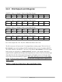
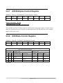
2.4.3
D/A Output Latch Register
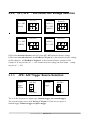
(WRITE) Base+4 : Channel 1 D/A Low Byte Data Format
Bit 7
Bit 6
Bit 5
Bit 4
Bit 3
Bit 2
Bit 1
Bit 0
D7
D6
D5
D4
D3
D2
D1
D0
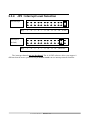
(WRITE) Base+5 :Channel 1 D/A High Byte Data Format
Bit 7
Bit 6
Bit 5
Bit 4
Bit 3
Bit 2
Bit 1
Bit 0
X
X
X
X
D11
D10
D9
D8
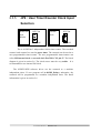
(WRITE) Base+6 : Channel 2 D/A Low Byte Data Format
Bit 7
Bit 6
Bit 5
Bit 4
Bit 3
Bit 2
Bit 1
Bit 0
D7
D6
D5
D4
D3
D2
D1
D0
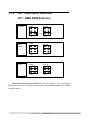
(WRITE) Base+7 :Channel 2 D/A High Byte Data Format
Bit 7
Bit 6
Bit 5
Bit 4
Bit 3
Bit 2
Bit 1
Bit 0
X
X
X
X
D11
D10
D9
D8
D/A 12 bits output data : D11..D0, D11=MSB, D0=LSB, X=don‘t care
The D/A converter will convert the 12 bits digital data to analog output. The low 8 bits of
D/A channel 1 are stored in address BASE+4 and high 4 bits are stored in address BASE+5.
The address BASE+6 and BASE+7 store the 12 bits data for D/A channel 2. The D/A output
latch registers are designed as a “double buffered” structure, so the analog output latch
registers will be updated until the high 4 bits digital data are written. If the user send the high
4 bits data first, the DA 12 bits output latch registers will update at once. So the low 8 bits
will be the previous data latched in register. This action will cause an error on DA output
voltage. So the user must send low 8 bits first and then send high 4 bits to update the 12
bits AD output latch register.
NOTE : Send low 8 bits first, then send high 4 bits.
A-812PG Hardware Manual----18