1
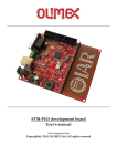
STM-103STK development board
Users Manual
Rev.A, April 2008
Copyright(c) 2008, OLIMEX Ltd, All rights reserved
INTRODUCTION:
The ARM Cortex-M3 processor is the latest generation of ARM processors
for embedded systems. It has been developed to provide a low-cost platform
that meets the needs of MCU implementation, with a reduced pin count
and low-power consumption, while delivering outstanding computational
performance and an advanced system response to interrupts. The ARM
Cortex-M3 32-bit RISC processor features exceptional code-efficiency,
delivering the high-performance expected from an ARM core in the memory
size usually associated with 8- and 16-bit devices.
The STM32F103 Performance Line family has an embedded ARM core and
is therefore compatible with all ARM tools and software. It combines the
high performance ARM Cortex-M3 CPU with an extensive range of
peripheral functions and enhanced I/O capabilities.
STM32-103STK is starter-kit board which allow you to explore the
complete features of the new ARM Cortex M3 STM32F103RBT6
microcontrollers produced by ST Microelectronics Inc. It have NOKIA 3310
BW 84x48 LCD, buttons, SD-MMC card, 3-axis digital accelerometer,
2.4Ghz RF transciever, Audio Input and Output, the power supply is made
from single 1.5V AA cell battery.
Some applications are USB Mass Storage device, Audio class device, HID
mouse device, CDC Virtual com port device, USB Wireless RF link.The UXT
connector allow access to all other UEXT modules produced by OLIMEX
like MOD-MP3, MOD-NRF24LR, MOD-NOKIA6610 etc to be connected
easily. In the prototype area customer can solder his own custom circuits
and to interface them to USB, CAN, RS232 etc.
BOARD FEATURES:
-
MCU: STM32F103RBT6 ARM 32 bit CORTEX M3™ with 128K Bytes
Program Flash, 20K Bytes RAM, USB, CAN, x2 I2C, x2 ADC 12 bit, x3
UART, x2 SPI, x3 TIMERS, up to 72Mhz operation
standard JTAG connector with ARM 2x10 pin layout for
programming/debugging with ARM-JTAG
USB mini connector
LCD NOKIA 3310 BW 84x48 pixels
1.5V battery connector with step-up converter
3-axis accelerometer
SD-MMC card
2.4 Ghz transciever with Nordic nRF24L01
Audio input
Audio output
user buttions x2
Joystick with 4 directions and push action
UEXT connector for other Olimex's modules connection like MOD-MP3,
etc.
RESET button
status LED
8 Mhz crystal oscillator
32768 Hz crystal and RTC backup battery connector
extension headers for all uC ports
PCB: FR-4, 1.5 mm (0,062"), soldermask, silkscreen component print
Dimensions: 90 x 65mm (3.5 x 2.5")
ELECTROSTATIC WARNING:
The STM32-103STK board is shipped in protective anti-static packaging.
The board must not be subject to high electrostatic potentials. General
practice for working with static sensitive devices should be applied when
working with this board.
BOARD USE REQUIREMENTS:
Cables:
1.8 meter A-to-miniUSB cable to connect to USB host.
Hardware:
ARM-JTAG, ARM-USB-OCD, ARM-USB-TINY or other ARM
JTAG compatible tool
Software:
ARM C compiler and debugger software, the possible options
are:
- free open source platform: GNU C compiler + OpenOCD
and Eclipse (support all low cost Olimex JTAG debuggers)
- commercial solution EW-ARM from IAR Systems AB,
require expensive J-LINK debugger
- CrossWorks from Rowley (supports all Olimex low cost
JTAG debuggers).
BOARD LAYOUT:
SCHEMATIC:
PROCESSOR FEATURES:
STM-103STK board use ARM 32-bit Cortex™-M3 CPU STM32F103RBT6
from ST Microelectronics with these features:
-
CPU clock up to 72Mhz
FLASH 128KB
RAM 20KB
DMA x7 channels
RTC
WDT
Timers x3+1
SPI x2
I2C x2
USART x3
USB x1
-
CAN x1 (multiplexed with USB so both can't be used in same time)
-
GPIO up to 51 (multiplexed with peripherials)
2 ADC 12-bit
operating voltage 2.0-3.6V
temperature -40C +85C
RS232:
STM32F103RBT6 have 3 USARTs which are available on the extension
headers. One of them can operate up to 4.5 Mbit/s, the other two up to
2.25 Mbit/s. They provide hardware management of the CTS and RTS
signals, IrDA SIR ENDEC support, are ISO 7816 compliant and have LIN
Master/Slave capability.
All USART interfaces can be served by the DMA controller.
SPI:
STM32F103RBT6 have 2 SPIs which able to communicate up to 18 Mbits/s
in slave and master modes in fullduplex and simplex communication
modes. The 3-bit prescaler gives 8 master mode frequencies and the frame
is
configurable
from
8-bit
to
16-bit.
The
hardware
CRC
generation/verification supports basic SD Card/MMC modes.
Both SPIs can be served by the DMA controller.
I2C:
STM32F103RBT6 have two I²C bus interfaces which can operate in multimaster and slave modes. They can support
standard and fast modes. They support dual slave addressing (7-bit only)
and both 7/10-bit addressing in master
mode. A hardware CRC generation/verification is embedded.
They can be served by DMA and they support SM Bus 2.0/PM Bus.
CAN:
The STM32F103RBT6 CAN is compliant with specifications 2.0A and B
(active) with a bit rate up to 1 Mbit/s. It can receive and transmit standard
frames with 11-bit identifiers as well as extended frames with 29-bit
identifiers. It has three transmit mailboxes, two receive FIFOs with 3 stages
and 14 scalable filter banks.
The CAN and USB share same pins PA11 and PA12, so you can’t use both
CAN and USB on same time.
USB:
The STM32F103RBT6 embeds a USB device peripheral compatible with the
USB Full-speed 12 Mbs. The USB interface implements a full speed (12
Mbit/s) function interface. It has software configurable endpoint setting
and suspend/resume support. The dedicated 48 MHz clock source is
generated from the internal main PLL.
The CAN and USB share same pins PA11 and PA12, so you can’t use both
CAN and USB on same time.
ADC:
STM32F103RBT6 have two 12-bit Analog to Digital Converters which share
up to 16 external channels, performing conversions in singleshot or scan
modes. In scan mode, automatic conversion is performed on a selected
group of analog inputs.
Additional logic functions embedded in the ADC interface allow:
- Simultaneous sample and hold
- Interleaved sample and hold
- Single shunt
The ADC can be served by the DMA controller.
An analog watchdog feature allows very precise monitoring of the converted
voltage of one, some or all selected channels. An interrupt is generated
when the converted voltage is outside the programmed thresholds. The
events generated by the standard timers (TIMx) and the Advanced Control
timer (TIM1) can be internally connected to the ADC start trigger, injection
trigger, and DMA trigger respectively, to allow the application to
synchronize A/D conversion and timers.
BLOCK DIAGRAM:
MEMORY MAP:
POWER SUPPLY CIRCUIT:
STM32-103STK can take power from these sources:
– 1.5V battery with DC/DC step up converter
– Vin signal on EXT1-11 pin.
- JTAG pin.1 or 2
The board power consumption is: about 30 mA when powered from the
USB port and 130mA when powered from 1.5V battery with all peripherials
and MCU running at full speed, there are different power saving modes
which may put STM32F103RBT6 in power sleep mode and in these modes
the consumption of the MCU is only few microampers.
RESET CIRCUIT:
STM32-103STK reset circuit is made with RC group R8 - 10K and C28100nF.
Although on the schematic is made provision for external reset IC such is
not necessary as STM32 have build-in brown out detector. Manual reset is
possible by the RESET button.
CLOCK CIRCUIT:
Quartz crystal 8Mhz is connected to STM32F103RBT6. Internal PLL circuit
can multiply this frequency up to 72Mhz.
32.768 KHz quartz crystal is connected to STM32F103RBT6 for it’s internal
Real Time Clock.
JUMPER DESCRIPTION:
EXT/BAT
3 pin, power supply select jumper.
EXT position
EXT/BAT
Allow power supply from mini-USB connector or EXT1(pin11).
The voltage supplied to EXT1(pin 11) must be between 5VDC
and 9VDC.
BAT position
EXT/BAT
Allow power supply from 1.5V AA (R6), no charge battery,
pluged in the BAT connector.
R-T
BAT_E
Connects JTAG TRST signal to STM32F103RBT6 RESET
Default state closed (shorted)
Connects 3.3V to STM32F103RBT6 Vbat pin.1
Default state closed (shorten), Vbat signal is also available to
EXT1 (pin 1) connector, so if you want to connect external
backup battery to the STM32F103RBT6 this jumper should be
opened (unshorted) and the external battery to be connected to
EXT1 (pin 1) connector(see connector description for EXT1
connector pining.).VBAT accept 2 - 3.6V.
USBP-E
Connects USB power supply to STM32F103RBT6 pin 24 PC4/
ADC14 and allow to detect if the board is connected to USB
host.
Default state closed (shorten)
LED-E
Connects STATUS LED to STM32F103RBT6 pin 53 PC12
Default state closed (shorten)
BOOT0, BOOT1
boot sequence select
B1_H/B1_L (Boot1_High/Boot1_Low)
B0_L/B0_H (Boot0_Low /Boot0_ High)
B1_H/B1_L
Default position:
Boot1 is log. 0
B0_L/B0_H
Boot0 is log. 0
CP_E
Card Present Enable – Allow PC1(pin 9) to detect Multi Media
Card present in socket. Log. 1 of PC1 – MMC present. Log.0 of
PC1 – Card absent.
Default state closed (shorten)
Write Protect Enable – Allow PC2(pin 10) to detect write
protected state of Multi Media Card. Log. 1 of PC2 – MMC no
write protected . Log.0 of PC2 – MMC is write protected.
Default state closed (shorten)
Connect 3.3V regulated voltage to STM32F103RBT6 power
pins. 3.3V_E jumper is used if you need to measure current
consumption of the microcontroller.
Default state closed (shorten)
WP_E
3.3V_E
INPUT/OUTPUT:
JOYSTICK
this is 4 directions plus center button, in the schematic the
joystick four directions switches are connected through resistors with
different values to PC5/ADC15 , the center button is connected to PC6;
BUTTON B1
Left button connected to PC13/TAMPER port;
BUTTON B2
Right button connected to PA0/WAKE-UP port;
LCD
NOKIA3310 84x48 pixel black and white LCD to SPI1 port;
ACCELEROMETER
Audio In
3-axis accelerometer connected to I2C1 port;
microphone with pre-amplifier connected to PA1 ADC;
Audio Out
audio amplifier connected to PA8 PWM output;
SD-MMC card connected to SPI2;
nRF24L01
connected to SPI1;
Power supply red LED with name PWR – indicates that 3.3V power supply
is applied.
CONNECTOR DESCRIPTION:
JTAG:
JTAG CONNECTOR PIN DESCRIPTIONS
Pin #
Signal Name
Pin #
Signal Name
1
TVCC 3.3V
2
TVCC 3.3V
3
TRST
4
GND
5
TDI
6
GND
7
TMS
8
GND
9
TCK
10
GND
11
NC
12
GND
13
TDO
14
GND
15
RST
16
GND
17
NC
18
GND
19
NC
20
GND
TMS
TCK
TDI
TDO
TRST
Input
Input
Test Mode Select. The TMS pin selects the next state in the TAP state machine.
Test Clock. This allows shifting of the data in, on the TMS and TDI pins.
It is a positive edgetriggered clock with the TMS and TCK signals that define the internal state
of the device.
Input
Test Data In. This is the serial data input for the shift register.
Output Test Data Output. This is the serial data output from the shift register. Data is shifted out of the
device on the negative edge of the TCK signal.
Input
Test Reset. The TRST pin can be used to reset the test logic within the EmbeddedICE logic.
EXT1
Pin #
Signal Name
Pin #
Signal Name
1
VBAT
2
PA3/USART2_RX/
ADC3/TIM2_CH4
3
PA9/USART1_TX/
TIM1_CH2
4
PA10/USART1_RX/
TIM1_CH2
5
RD0/OSC_IN
6
PC12/LED
7
PC4/ADC14/
USB_PRESENT
8
PC3/ADC13/
STNBY
9
PA2/USART2_TX/
ADC2/ITIM2_CH3
10
NRST
11
VIN
12
+5.0V
13
3.3V
14
GND
Pin #
Signal Name
Pin #
Signal Name
1
PB0/ADC8/TIM3_CH3
2
PB1/ADC9/TIM3_CH4
3
PB8/TIM4_CH3
4
PB9/TIM4_CH4
5
SCL2
6
SDA2
7
PC0/ADC10
8
CP
9
WP
10
3.3V_A
11
AGND
12
+5.0
13
3.3V
14
GND
EXT2
UEXT
Pin #
Signal Name
Pin #
Signal Name
1
VCC 3.3V
2
GND
3
TX2
4
RX2
5
SCL2
6
SDA2
7
SPI2_MISO
8
SPI2_MOSI
9
SPI2_SCK
10
SPI2_NSS
SD-MMC
Pin #
Signal Name
Pin #
Signal Name
1
SPI2_NSS
2
SPI2_MOSI
3
GND
4
VCC
5
SPI2_SCK
6
GND
7
SPI2_MISO
8
10K to 3.3V
9
10K to 3.3V
10
WP_E
11
to pin 14
12
to pin 15
13
CP_E
14
2K to 3.3V
15
2K to 3.3V
Pin #
Signal Name
1
VBUS
2
USBDM
3
USBDP
4
NC
5
GND
USB
AVAILABLE DEMO SOFTWARE:
–
–
–
–
–
–
–
USB mouse with the 3-axis accelerometer
USB class Audio device
USB mass storage
USB Virtual com port
USB RF Virtual com port bridge
Ball game with accelerometer
OpenOCD demo project
ORDER CODE:
STM32-103STK – assembled and tested (no kit, no soldering required)
How to order?
You can order to us directly or by any of our distributors.
Check our web www.olimex.com/dev for more info.
All boards produced by Olimex are ROHS compliant
Revision history:
REV.A
- create April 2008
Disclaimer:
© 2008 Olimex Ltd. All rights reserved. Olimex®, logo and combinations thereof, are registered trademarks of
Olimex Ltd. Other terms and product names may be trademarks of others.
The information in this document is provided in connection with Olimex products. No license, express or implied
or otherwise, to any intellectual property right is granted by this document or in connection with the sale of Olimex
products.
Neither the whole nor any part of the information contained in or the product described in this document may be
adapted or reproduced in any material from except with the prior written permission of the copyright holder.
The product described in this document is subject to continuous development and improvements. All particulars of
the product and its use contained in this document are given by OLIMEX in good faith. However all warranties
implied or expressed including but not limited to implied warranties of merchantability or fitness for purpose are
excluded.
This document is intended only to assist the reader in the use of the product. OLIMEX Ltd. shall not be liable for
any loss or damage arising from the use of any information in this document or any error or omission in such
information or any incorrect use of the product.