1
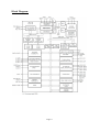
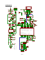
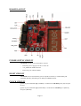
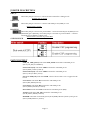
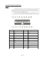
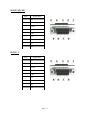
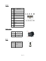
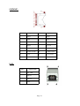
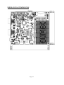
LPC-P2148 development board
Users Manual
All boards produced by Olimex are ROHS compliant
Rev.D, November 2009
Copyright(c) 2010, OLIMEX Ltd, All rights reserved
Page 1
INTRODUCTION:
LPC-P2148 is prototype board for LPC2148 ARM7TDMI-S microcontroller with USB
2.0 Full-speed device, multiple UARTs, SPI, SSP to I2C-bus and on-chip SRAM up
to 40 kB, produced by NXP Semiconductors.
With LPC-P2148 you can explore the features of LPC21XX family on budged, the
board has everything necessary to build simple applications: reset and oscillator
circuits, JTAG port for programming and debugging, USB, RS232, SD/MMC,
Buzzer, three status LEDs, potentiometer and two user buttons.
There are plenty of GPIOs on extension headers and also a prototype area where
you can connect your additional circuits.
BOARD FEATURES:
-
MCU: LPC2148 16/32 bit ARM7TDMI-S™ with 512K Bytes Program Flash, 42K
Bytes RAM, USB 2.0, RTC, 10 bit ADC 2.44 uS, 2x UARTs, 2x I2C, SPI, 2x 32bit
TIMERS, 6x PWM, 8x CCR, 1x DAC, WDT, 5V tolerant I/O, up to 60MHz
operation
-
standard JTAG connector with ARM 2x10 pin layout for
programming/debugging with ARM-JTAG
-
USB connector, USB link LED
-
Two channel RS232 interface and drivers
-
SD/MMC card connector
-
two buttons
-
trimpot connected to ADC
-
two status LEDs
-
Buzzer
-
UEXT - 10 pin extension connector for Olimex addition peripherals like MP3,
RF2.4Ghz, RFID etc. modules
-
2x SPI connectors
-
I2C connector
-
on board voltage regulator 3.3V with up to 800mA current
-
single power supply: 6V AC or DC required
-
power supply LED
-
power supply filtering capacitor
-
RESET circuit with external control of Philips ISP utility via RS232
-
RESET button
-
DBG, BSL slide switch
-
JRST jumper for enable/disable external RESET control by RS232
-
12 Mhz crystal on socket
-
32768 Hz crystal and RTC backup battery connector
Page 2
-
extension headers for all uC ports
-
PCB: FR-4, 1.5 mm (0,062"), soldermask, white silkscreen component print
-
Dimensions: 110 x 100 mm (4.3 x 3.9 ")
ELECTROSTATIC WARNING:
The LPC-P2148 board is shipped in protective anti-static packaging. The board must
not be subject to high electrostatic potentials. General practice for working with
static sensitive devices should be applied when working with this board.
BOARD USE REQUIREMENTS:
Cables: The cable you will need depends on the programmer/debugger you use. If
you use ARM-USB-OCD, you will need RS232 cable and 1.8 meter USB A-B cable, if
you use ARM-USB-TINY, you will need 1.8 meter USB A-B cable and if you use
ARM-JTAG, you will need LPT cable.
Hardware: Programmer/Debugger – one of the Olimex ARM Programmers: ARMUSB-OCD, ARM-USB-TINY, ARM-JTAG.
Software: ARM C compiler and JTAG programmer, the possible options are:
- open source platform: GNU C compiler + OpenOCD and Eclipse
PROCESSOR FEATURES:
LPC-P2148 board use Single-chip 16-bit/32-bit microcontroller LPC2148 from NXP
Semiconductors with these features:
–
16-bit/32-bit ARM7TDMI-S microcontroller
–
40 kB of on-chip static RAM and 512 kB of on-chip flash memory. 128-bit wide
interface/accelerator enables high-speed 60 MHz operation.
–
In-System Programming/In-Application Programming (ISP/IAP) via on-chip
boot loader software. Single flash sector or full chip erase in 400 ms and
programming of 256 B in 1 ms.
–
EmbeddedICE RT and Embedded Trace interfaces offer real-time debugging
with the on-chip RealMonitor software and high-speed tracing of instruction
execution.
–
USB 2.0 Full-speed compliant device controller with 2 kB of endpoint RAM. In
addition, the LPC2146/48 provides 8 kB of on-chip RAM accessible to USB by
DMA.
–
Two 10-bit ADCs provide a total of 14 analog inputs, with conversion times as
low as 2.44 ms per channel.
–
Single 10-bit DAC provides variable analog output
Page 3
–
Two 32-bit timers/external event counters (with four capture and four compare
channels each), PWM unit (six outputs) and watchdog.
–
Low power Real-Time Clock (RTC) with independent power and 32 kHz clock
input.
–
Multiple serial interfaces including two UARTs (16C550), two Fast I2C-bus (400
kbit/s), SPI and SSP with buffering and variable data length capabilities.
–
Vectored Interrupt Controller (VIC) with configurable priorities and vector
addresses.
–
Up to 45 of 5 V tolerant fast general purpose I/O pins in a tiny LQFP64
package.
–
Up to 21 external interrupt pins available.
–
60 MHz maximum CPU clock available from programmable on-chip PLL with
settling time of 100 ms.
–
On-chip integrated oscillator operates with an external crystal from 1 MHz to 25
MHz.
–
Power saving modes include Idle and Power-down.
–
Individual enable/disable of peripheral functions as well as peripheral clock
scaling for additional power optimization.
–
Processor wake-up from Power-down mode via external interrupt or BOD.
–
Single power supply chip with POR and BOD circuits:
–
CPU operating voltage range of 3.0 V to 3.6 V (3.3 V ± 10 %) with 5 V
tolerant I/O pads.
Page 4
Block Diagram:
Page 5
MEMORY MAP:
Page 6
P1 .1 6
P1.1 7
P1.1 8
P1.1 9
P1.20
P1.21
P1 .22
P1 .23
P1 .24
P1 .2 5
R6
10K
R5
10K
R2
10 K
R3
10 K
R4
10 K
1
3
5
7
9
11
13
15
17
19
Page 7
VREF
2
4
6
8
10
12
14
16
18
20
2
1
1 00 n
1 00 n
+
10u F/6.3 V
C6
C2
C3
BAT54 C
D6
C4
1 0p
C5
1 0p
0
1 00 n
C8
3 .3 V
VREF
1 00 n
C1
R18
G ND
32768/6pF
Q2
59
7
63
6
18
25
42
50
23
43
51
49
5
3
LPC2 14 X
VSSA
VDD3(A)
VREF
VSS1
VSS2
VSS3
VSS4
VSS5
VDD3-1(I/O)
VDD3-2(I/O)
VDD3-3(I/O)
VBAT
RTCX2
RTCX1
P1.24/TRACECLK
P1.25/EXTIN0
P1.26/RTCK
P1.27/TDO
P1.28/TDI
P1.29/TCK
P1.30/TMS
P1.31/TRST
RST
X2
X1
P0.25/AD0.4/AOUT
USBD+
USBDP0.28/AD0.1/CAP0.2/MAT0.2
P0.29/AD0.2/CAP0.3/MAT0.3
P0.30/AD0.3/EINT3/CAP0.0
P0.31/UP_LED/CONNECT
P0.16/EINT0/MAT0.2/CAP0.2
P0.17/CAP1.2/SCK1/MAT1.2
P0.18/CAP1.3/MISO1/MAT1.3
P0.19/MAT1.2/MOSI1/CAP1.2
P0.20/MAT1.3/SSEL1/EINT3
P0.21/PWM5/AD1.6/CAP1.3
P0.22/AD1.7/CAP0.0/MAT0.0
P0.23/VBUS
P0.8/TXD1/PWM4/AD1.1
P0.9/RXD1/PWM6/EINT3
P0.10/RTS1/CAP1.0/AD1.2
P0.11/CTS1/CAP1.1/SCL1
P0.12/DSR1/MAT1.0/AD1.3
P0.13/DTR1/MAT1.1/AD1.4
P0.14/DCD1/EINT1/SDA1
P0.15/RI1/EINT2/AD1.5
57
RST
12MHz
61
6
7
8
9
R32
1 0K
R 16
2K
10 K
R10
GND
U1
MCP13 0T
VCC 2
P0.2 8
P0.29
AD03
AO UT
P0.21
P0.22
P0.12
P0.13
BSL
1 RESET
C28
3 9p
C2 7
3 9p
AD03
CONNECT
B2
SCK1
MISO1
MOSI1
SSEL1
BUZZ1
BUZZ2
BSL
B1
TXD1
RXD1
TXD0
RXD0
SCL0
SDA0
SCK0
MISO0
MOSI0
SSEL0
62 Q 1
9
10
11
13
14
15
17
46
47
53
54
55
1
2
58
33
34
35
37
38
39
41
45
19
21
22
26
27
29
30
31
R 17
2K
3 .3V
1
2
3
4
5
6
7
8
9
R S2 32 _0 /ICSP
TX1OUT
RX1IN
6
5
4
3
2
1
2K
3.3V
R 40
10 K
18p
18p
R39
C 11
C 12
R35
R24
R25
R3 4
SPI0
I2C
SSEL 1
4
3
2
1
D4
1 N41 48
3 .3V
T1
BC84 6
2
1
ON
3 .3V
R27
33 0
LED2
3 .3V
R 12
NA
R 29
1.5 K
R 30
33 0
3.3 V
C 10
10n
+5V_ USB
R36
10 0K
USB_L INK
ye llow
Q3
BC 807
3.3V
100 n
C1 4
1
2
3
4
SPI1
BUZZ2
BUZZ1
10 K
R 33
USB_B
S HIE L D
MISO1
3.3V
3 .3 V
3.3 V
33 K
R37
3.3V
SCL0
SDA0
MISO0
MOSI0
SCK0
SSEL0
R2 2
2K
P1.25
10 K
10 K
MISO1
SCK1
R15
R41
MISO1
P1.24
SCK1
0
C9
13
15
1
2
3
4
5
6
7
8
9
10
14
UEXT-1
UEXT-2
UEXT-3
UEXT-4
UEXT-5
UEXT-6
UEXT-7
U EXT-8
U EXT-9
UEXT-1 0
AD03
CP1
CP2
CD/DAT3/CS
CMD/DI
VSS1
VDD
CLK/SCLK
VSS2
DAT0/DO
DAT1/RES
DAT2/RES
WP1
WP2
SD/MMC
SD-CARD
3 .3V
47uF/6.3V
USB
SCK1
MISO1
MOSI1
SSEL1
R31
R1 9 NC
33 K
R2 3 2 K
R38
R4 2
220
AN_TR
10 K
TXD1
L1
4 70 nH
B2
R14
10 K
3.3 V
MOSI1
3.3V
33 0
R28
3
2
1
B2
BUZZER
RXD1
B1
R13
10 K
3.3 V
SSEL1
MOSI1
3 .3 V
R4 3
2 2K
B1
R44
10 K
3.3 V
6
5
4
3
2
1
T2
BC84 6
R11
22 K
3.3 V
BSL
SCK1 ,MISO ,MO SI,SSEL1
1 0K
R26
33 0
LED1
10 K
33
33
3 .3 V
R9
2 2K
RST
SW -TAKT6
RST
R8
10 K
3.3 V
USB
3.3V
2
1
3 .3V
BAT
32
28
24
64
60
56
52
20
P1.24
P1.25
RTCK
TDO
TDI
TCK
TMS
TRST
GND15
C2 0
1 00 n
13 RX0IN
8 RX1IN
14 TX0OUT
7 TX1OUT
C 19
100 n
C18
10 0n
P0.0/TXD0/PWM1
P0.1/RXD0/PWM3/EINT0
P0.2/SCL0/CAP0.0
P0.3/SDA0/MAT0.0/EINT1
P0.4/SCK0/CAP0.1/AD0.6
P0.5/MISO0/MAT0.1/AD0.7
P0.6/MOSI0/CAP0.2/AD1.0
P0.7/SSEL0/PWM2/EINT2
16VCC
U2 PW R
R1IN
R2IN
T1OUT
T2OUT
6
2
RS232 _1
RS1/UEXT
VR EF-3 .3V
JTAG
P1.16/TRACEPKT0
P1.17/TRACEPKT1
P1.18/TRACEPKT2
P1.19/TRACEPKT3
P1.20/TRACESYNC
P1.21/PIPESTAT0
P1.22/PIPESTAT1
P1.23/PIPESTAT2
U3
3 .3V
R1OUT
R2OUT
T1IN
T2IN
V-
V+
1
2
3
4
5
D2
2
1
R1
10 K
16
12
8
4
48
44
40
36
G ND
12
9
11
10
C2-
C2+
C1-
C1+
U2
MAX32 32
+
DBG _ E
TRST
TDI
TMS
TCK
RTCK
TDO
RST
R45
NA
+
P1.16
P1.17
P1.18
P1.19
P1.20
P1.21
P1.22
P1.23
47 uF/6.3V
RXD0
TXD0
TXD1
5
C17 4
10 0n
3
C1 6 1
1 00 n
D3
3.3 V
R21
39 0/1 %
+
C13
R2 0
2 40 /1 %
3.3 V
1N4148
P1.20
R7
47 0
ADJ/GND
OUT
3.3 V
4
3
P1.[16 ..2 5],RTCK,TDO ,TDI,TCK,TMS,TRST
h ttp ://ww w.olimex.com/de v
CO PYRIG HT(C) 20 09 , O limex Ltd .
Rev. D
VIN
PW R
IN
1 N41 48
VR1(3.3V)
L M11 17
D5
1N4148
P1.16
P1.17
P1.18
P1.19
P1.20
P1.21
P1.22
P1.23
P1.24
P1.25
C7
47 0u F/1 6VDC
B-DIL 3
VIN
SMA1 N58 19
D1
ICSP
1
2
LPC-P2148
6VAC
9VDC
PW R_JACK
G1
+5V_USB
SCHEMATIC
3
BOARD LAYOUT
POWER SUPPLY CIRCUIT
LPC-P2148 can take power from three sources:
–
External power supply 9.0V DC or 6.0V AC.
–
+5V_USB from USB connector
–
Extension pins VIN and GND
RESET CIRCUIT
LPC-P2148 reset circuit includes pin 15 of JTAG connector, U1 (MCP130T), D4
(1N4148), R8 (10k), LPC2148 pin 57 (RST) and RESET button.
CLOCK CIRCUIT
Quartz crystal with name Q1 (12 MHz) is connected to LPC2148 pin 61 (X2) and pin
62 (X1).
Quartz crystal with name Q2 (32.768 kHz) is connected to LPC2148 pin 3 (RTCX1)
and pin 5 (RTCX2).
Page 8
JUMPER DESCRIPTION
DBG_E
When this jumper is shorted – selects the microcontroller's debug mode.
Default state is closed.
VREF-3.3V
When this jumper is shorted – connects LPC2148 pin 63 (VREF) to 3.3V.
Default state is closed.
RS1/UEXT
When this jumper is shorted in position RS1 – connects LPC2148 pin 34 (RXD1) to U2
(MAX3232) pin 9 (R2OUT); when this jumper is shorted in position UEXT - connects
LPC2148 pin 34 (RXD1) to UEXT pin 4.
Default state is shorted in position RS1.
SLIDE SWITCH
INPUT/OUTPUT
USB_UP_ LED (yellow) with name USB_LINK connected to LPC2148 pin 17
(P0.31/UP_LED/CONNECT).
Status LED1 (red) with name LED1 connected to LPC2148 pin 35
(P0.10/RTS1/CAP1.0/AD1.2).
Status LED2 (red) with name LED2 connected to LPC2148 pin 37
(P0.11/CTS1/CAP1.1/SCL1).
Power-on LED (red) with name PWR – this led shows that +3.3V is applied to the
board.
User button with name B1 connected to LPC2148 pin 45
(P0.15/RI1/EINT2/AD1.5).
User button with name B2 connected to LPC2148 pin 46
(P0.16/EINT0/MAT0.2/CAP0.2).
Reset button with name RST connected to LPC2148 pin 57 (RST).
Trimpot with name AN_TR connected to LPC2148 pin 15
(P0.30/AD0.3/EINT3/CAP0.0).
BUZZER connected to LPC2148 pin 38 (P0.12/DSR1/MAT1.0/AD1.3) and pin 39
(P0.13/DTR1/MAT1.1/AD1.4).
Page 9
CONNECTOR DESCRIPTIONS
JTAG:
The JTAG connector allows the software debugger to talk via a JTAG (Joint
Test Action Group) port directly to the core. Instructions may be inserted and
executed by the core thus allowing LPC2148 memory to be programmed with code
and executed step by step by the host software.
For more details refer to IEEE Standard 1149.1 - 1990 Standard Test Access
Port and Boundary Scan Architecture and LPC2148 datasheets and users manual.
Pin #
Signal Name
Pin #
Signal Name
1
+3.3V
2
+3.3V
3
TRST
4
GND
5
TDI
6
GND
7
TMS
8
GND
9
TCK
10
GND
11
RTCK
12
GND
13
TDO
14
GND
15
RST
16
GND
17
NC
18
GND
19
NC
20
GND
Page 10
RS232_0/ICSP:
Pin #
Signal Name
1
NC
2
TX0OUT
3
RX0IN
4
Slide Switch pin 3
5
GND
6
NC
7
Slide Switch pin 4
8
NC
9
NC
RS232_1:
Pin #
Signal Name
1
NC
2
TX1OUT
3
RX1IN
4
NC
5
GND
6
NC
7
NC
8
NC
9
NC
Page 11
UEXT:
Pin #
Signal Name
1
3.3V
2
GND
3
TXD1
4
Via JMP RS1/UEXT to RXD1
5
SCL0
6
SDA0
7
MISO0
8
MOSI0
9
SCK0
10
SSEL0
PWR_JACK:
Pin #
Signal Name
1
Power Input
2
GND
BAT:
Pin #
Signal Name
1
to 3.3V
2
GND
Page 12
SD/MMC:
Pin #
Signal Name
Pin #
Signal Name
1
SSEL1
2
MOSI1
3
GND
4
+3.3V
5
SCK1
6
GND
7
MISO1
8
PULL-UP
9
PULL-UP
10
P1.24
11
Via R23 to GND
12
Via R22 to GND
13
P1.25
14
PULL-DOWN
15
PULL-DOWN
USB:
Pin #
Signal Name
1
+5V_USB
2
USB_D-
3
USB_D+
4
GND
Page 13
EXT:
Page 14
I2C
The I2C-bus is bidirectional, for inter-IC control using only two wires: a serial clock line (SCL),
and a serial data line (SDA). Each device is recognized by a unique address and can operate as either a
receiver-only device. Transmitters and/or receivers can operate in either master or slave mode,
depending on whether the chip has to initiate a data transfer or is only addressed. The I2C-bus is a
multi-master bus, it can be controlled by more than one bus master connected to it.
The I2C-bus implemented in LPC2148 supports bit rates up to 400 kbit/s (Fast I2C-bus).
Features:
–
–
–
–
–
–
–
–
–
Compliant with standard I2C-bus interface.
Easy to configure as master, slave, or master/slave.
Programmable clocks allow versatile rate control.
Bidirectional data transfer between masters and slaves.
Multi-master bus (no central master).
Arbitration between simultaneously transmitting masters without corruption of serial
data on the bus.
Serial clock synchronization allows devices with different bit rates to communicate via
one serial bus
Serial clock synchronization can be used as a handshake mechanism to suspend and
resume serial transfer.
The I2C-bus can be used for test and diagnostic purposes.
SPI
The SPI is a full duplex serial interface, designed to handle multiple masters and slaves
connected to a given bus. Only a single master and a single slave can communicate on the interface
during a given data transfer. During a data transfer the master always sends a byte of data to the
slave, and the slave always sends a byte of data to the master.
Features:
–
–
–
–
Compliant with SPI specification.
Synchronous, Serial, Full Duplex, Communication.
Combined SPI master and slave.
Maximum data bit rate of one eighth of the input clock rate.
Page 15
MECHANICAL DIMENSIONS
Page 16
AVAILABLE DEMO SOFTWARE
–
USB mouse demo for EW-ARM 5.40
–
board peripherials demo code for EW-ARM 4.42
–
RF link with MOD-NRF24LR
–
OpenSource USB stack for LPC
–
BLINK-LED project with GCC+OpenOCD+Eclipse
–
OpenOCD + Eclipse set of projects 1.00 include flash write make file for LPCP2148.
Page 17
ORDER CODE
LPC-P2148 – assembled and tested (no kit, no soldering required)
How to order?
You can order to us directly or by any of our distributors.
Check our web www.olimex.com/dev for more info.
Revision history:
REV. D - create November 2009
Page 18
Disclaimer:
© 2010 Olimex Ltd. All rights reserved. Olimex®, logo and combinations thereof, are registered trademarks of
Olimex Ltd. Other terms and product names may be trademarks of others.
The information in this document is provided in connection with Olimex products. No license, express or implied
or otherwise, to any intellectual property right is granted by this document or in connection with the sale of
Olimex products.
Neither the whole nor any part of the information contained in or the product described in this document may be
adapted or reproduced in any material from except with the prior written permission of the copyright holder.
The product described in this document is subject to continuous development and improvements. All particulars
of the product and its use contained in this document are given by OLIMEX in good faith. However all warranties
implied or expressed including but not limited to implied warranties of merchantability or fitness for purpose are
excluded.
This document is intended only to assist the reader in the use of the product. OLIMEX Ltd. shall not be liable for
any loss or damage arising from the use of any information in this document or any error or omission in such
information or any incorrect use of the product.
Page 19