1
DG24
UsertsManual
ffi
RealTimeDevices,
Inc.
"Accessingthe Analog World',"
ISO9001 and AS9100 Certified
artJt,u
\)t-
a
UsertsManual
ffi
REALTIMEDEVICES,
INC.
820 NorthUniversity
Drive
PostOfficeBox906
StateCollege,
Pennsylvania
16804
Phone:(814)234-8087
FAX:(814)234-5218
Publishedby
RealTime Devices,Inc.
820N. UniversityDr.
P.O.Box 906
StateCollege,PA 16804
Copyright@ 1992by RealTime Devices,Inc.
All righrsreserved
Prinredin U.S.A.
Rev.C 9234
Thbleof Contents
INTRODUCTION
t-l
What ComesWith Your
BoardAccessories
..........
CHAPTER 1 - BOARD SETTINGS
Factory-Configured
Swiah andJumperSettings
...............1-3
P2- BaseAddress(FacorySetting:300hex(768decimal) .................
..............14
P3- IntemrptSourceandChannelSelect(FactorySetting:Disabled)
................14
P4- Digial Ip Direction(ModelDG2.E Only)@acorySetting:IIrI)...............
...................l-5
P5- Pull-up/Pull-down
Select(FactorySeuing:+5V (Pull-up))
.........................1-5
Sl/S2lS3- Buffer BypassSwitches@62r''IBOnly) (FacrorySeuing:OPEN(Not Bypassed))....................
t-e
Pull-uplPull-downResistorson DigiralInputlines (RNI-RN4)
...........1-g
Pull-downResisorson BufferedDigiralOutputLines(RN5-RN8)
......l-9
CHAPTER 2 - BOARD INSTALLATION
Connecting
ConnectingtheExternalIntemlpt
Connectingthe Reset
CHAPTER 3 - HARDWARE DESCRIPTION
DigitalVO, 8255ProgrammablePeripheral
Interface......
Intemrpts.........
CHAPTER 4 - BOARD OPERATION AND PROGRAMMING
2-l
.............24
....................
3-I
......................3-3
......4-l
BA + 3: 8255PPI ControlWord (WrireOnly) ...
ClearingandSettingBits in a Port...........
8259Programmable
IntemrptController
IntemrptMaskRegister(Il"R) ..........
(EOI)Command
End-of-Intemrpt
WhatExactlyHappens
WhenanIntemrpt
Occurs?
Intemrpts
Yourhograms...................
Using
in
......................4-7
...................4-9
........4-g
.......................4_9
.........4-g
WritinganInrcmrpt
(lSR)............
Rourine
Service
Saving
(IMR)andInterrupr
thesranupInremrpr
MaskRegister
vecror
Restoring
theStartup
IMR andInterrupr
Vector
Common
Interrupt
Misnkes
APPENDIX A - DG24SPECIFICATIONS
APPENDIX B - P6 CONNECTORPIN ASSIGNMENTS..........
APPENDIXC - COMPONENT
DATA SHEETS
APPENDIXD - WARRANTY
........................4-9
..........4-l
I
.....4-lI
...............4-l
I
...........A-1
B-l
.........c-l
...................
D-t
LIST OF ILLUSTRATIONS
l-l
t-2
l-3
t4
l-5
l-6
1-7
l-8
2-l
3-l
w
INTRODUCTION
i-l
The DG24 is a generalpurposedigital I/O boardfor usein the IBM PCIXT/AT or compatiblecompurer.
Installedwithin a singleshortor full-sizeexpansionslot in thecomputer,rheDG24features:
.
.
.
.
.
.
24 TTLICMOS 8255-basedprogrammabledigital I/O lines,
OptionalTTL bufferedourpursfor high driving capability (/B model),
Optionalpull-up/pulldown resistors,
SimpleI ) or strobedI/O operation,
Hardwareenabledintemrprs(IRQ2-IRQ7),
BASIC, Turbo Pascal,andTurbo C sourcecode.
The following paragraphsbriefly describethe major functionof the board.A moredetaileddiscussionof board
functionsis includedin Chapter3, Hardware Operatbn, andChapter4, Board Operarionand Programming.The
boardsetupis describedin Chapterl, Board Settings.
Digital VO
The DG24 has24 TTL/CMOS+ompatibledigiral VO lines which canbe direcrly interfacedwith exrernal
devicesor signalsto senseswitchclosures,triggerdigitalevens,or activatesolid-state
relays.Theselinesare
providedby 0reon-board8255programmableperipheralinterfacechip. The unbuffered8255can be operatedin any
one of the 8255's threemodes. If you havepurchasedtheDG24E with TTL buffers for high driving capacity,the
8255canbe operatedin Mode 0 whenthe buffersare installed.CMOS buffen are availableon request.
Padsfor installing andactivatingpull-up or pull-down resistorsare includedon the board.Installationproceduresaregivenat theendof Chapterl, Board Settings.
IVhat ComesWith Your Board
You receivethe following itemsin your DG24package:
. DG24 or DGZ4|B(wirh TTL buffers)interfaceboard
. Softwarediskettewith BASIC, Tubo Pascal,andTurbo C sourcecode
. User'smanual
If any item is missingm damaged,
pleasecall RealTime Devices'CustomerServiceDepartmentat
(814)234-8087.If you requireserviceoutsidetheU.S.,contactyour localdisribuor.
Board Accessories
In addition to the items irrcludedin your DG24package,RealTime Devicesoffers a full line of accessories.
Call your local disributor or our main office for moreinformationabouttheseaccessories
and for help in choosing
the bestitems to supportyour board'sapplication.
Accessoriesfor the DG24 includethe TB40 terminalboardandXB40 protorype/terminalboard for prorotype
developmentand easysignalaccess,and the )P40 flat ribbon cableassemblyfor externalinterfacing.
UsingThis Manual
This manualis intendedn help you install your new boardandget it runningquickly, while also providing
enoughdetail aboutthe boardand its functionsso ttratyou canenjoy maximumuseof its featuresevenin the most
complexapplications.We assumethat you alreadyhavean undersundingof dataacquisitionprinciplesand that you
can customizethe examplesoftwareor write your own applicationsprognms.
t-3
When You NeedHelp
This manualand the exampleprogams in the softwarepackageincludedwith your boardprovide enough
informationto properlyuseall of theboard'sfeatures.If you haveanyproblemsinstallingor usingrhisboard,
(814)234-8087,duringregularbusinesshouls,easternstandardtime or
contactour TechnicalSupportDepartment,
easterndaylighttime,or senda FAX requestingassistance
to (814)234-5218.Whensendinga FAX request,please
your name,your telephone
includeyourcompany'snameandaddress,
number,anda brief descriptionof the
problem.
CHAPTER 1
BOARDSETTINGS
The DG24boardhasjumpersettingsyou canchangeif necessaryfor your application.The factorysettingsarelistedandshown
on a diagramin the beginningof this chapter.Shouldyou needto
changethesesettings,usetheseeasy-to-followinstructionsbefore
you installtheboardin your computer.
NotethatDIP switchesSl, 52, and53 hasbeenprovidedto
bypassthe 8255buffersif you havetheDG24E bufferedmodel.
Also notethatby installingresistorpacksat RNl-RN4 and
settingthejumperson P5,you canconfigureyour digital input
linesto be pulledup or pulleddown.This procedureis explained
neartheendof this chapter.
RN5 throughRN8 areprovidedto installresistorpacksfor
portsconfiguredasbufferedoulputs.Thesepull-downresistor
packsaredescribedat theendof this chapter.
r-2
Factory-ConfiguredSwitchand Jumper Settings
Tablel-l liss thefactorysettingsof the user-configurable
jumperandswircheson theDG24board.Figure1-1
showsthe boardlayout andthe locationsof ttrefacory-setjumpers.The following paragraphsexplain how ro
changethe facory settings.Pay specialattentiono the settingof P2, the baseaddressjumper, to avoid address
contentionwhen you first useyour boardin your system.
Table1-l - FactorySettings
Swltch/
Jumper
FactorySettlngs
(JumpersInstall6d)
FunctionControlled
P2
Sels the base address to 1 of 8 l/O oorts
300 hEx (768 decimal)
P3
Connects1 or moreol ihe 3 interrupt
sourcesto an
interrupl
channel
Interrupt
channelsdisabled
P4
Setsthe directionof buffereddigitall/O linEson
PortsA, B, CL & CH setas inputs
PortsA, B, CL & CH (activeon DG24Bmodelonly) (4 jumpersinstalled
on lN pins)
P5
Setsresistornetworks
RN1-RN4
for PortsA, B, CL
& CH as pull-ups(+5V)or pull-downs
(GND);active
onlywhenoptionalresistorpacksareinstallsd
(nojumpersinstalled)
Disabled
S1
Bypasses8255PortA buffersfor Mode2 operation
(DG24|Bonly)
Open(butfersnotbypassed)
s2
Bypasses8255PortB bullErsfor Mode1 operation
(DG2{B only)
Open(buffersnotbypasssd)
S3
Bypasses8255PortC buffersfor Modes1 & 2
operation(DG24/Bonly)
Open(buffersnotbypassed)
DG24
r'[fiiT?:
ilaea3m*m
Gd6-6-6?t6-6-d6t
Gtr6-d66r
66-dd6.E
G6o666E-6-dO
Pm
'9 E6E666E
Affini"-"--,siffiFl
rg, EZSEE?EE
|9
E668661d
b,""o,
gJ
.oooJooo,-oo-ooooo-,
-l5"Lse's
&eg*,,.
I
tfi'*"--_-lt?*s'?..
9qOOOOO,- trOOOOOO
trOOOOOOOOO
u EOOOOOOOOO
\9
u
; GAo6:66| * @
*(trE6-d6656do3@
oooooooooooooooooooo
l.e-;.3r
trooo@
P:rptrtl
",ElFtrE
R..l
Tin.
D.yic.s,
|rc. St tr ColLg.,
PA t68(x
cro
US
clt
Fig.1-1- BoardLayoutShowingFactory-Configured
Settings
l-3
P2 - BaseAddress(Factory Setting:300 hex (768decimat))
Oneof themostcommoncausesof failurewhenyou arefirst trying your boardis addresscontention.Someof
yolu computer'sIr0 spaceis alreadyoccupiedby intemal I/O and orherperipherals.When the DG24 boardattempts
to useVO addresslocationsalreadyusedby anotherdevice,contentionresultsand the boarddoesnot work.
To avoidthisproblem,theDGZ hasa headerconnector,P2, whichletsyou selectanyoneof eightstarting
in thecomputer'sVO. Shouldthefactorysettingof 300hex (768decimal)be unsuitablefor your system,
addresses
you canselecta different baseaddress.Theseaddresses
are,from left o right on p2:
Heradeclmal
Declmal
200
512
24A
576
280
640
2C0
704
300
768
340
932
380
896
3C0
960
To changethe baseaddresssetting,removettrejumper from the fifth from right paii of pins (300 hex) and,
usingFigure l-2 asa guide,install it in the desiredlocation.Recordthe new baseaddresssettingon the able inside
the backcoverof this manual.
te8E8e8E
ot
P2
6t
(\l
N
ci,
c,
c)
g|t
o.oo?ooo
I
aooaaooo
Fig.1-2 -
Base AddressJumper, p2
P3 - Interupt Sourceand ChannelSelect(FactorySetting: Disabled)
This headerconnector,shownin Figure 1-3,lets you connectone of threeintemrpt sourceso an intemrpt
channelfor intemrpt generation.Thesesourcesare:PC0,which is ttreINTRB signalfrom the 8255ppl; pCj, which
is the INTRA signal from 0re8255PPI; andEXTINT, an externalintemrpt you canrouteonlo the boardthroughthe
P6llO connector.Eachsourcehastwo IRQ channelsavailableto avoid conten[ion.Whenselectingthe intenupt and
channelyou desire,be surethat ttreIRQ channelis not usedby otherdevicesyottr computersystem.Note that it is
possibleto usemore thanone interruptsourceon the DG24.To connectan intemrpt source,placethejumper across
thedesiredsetof pins.Figure1-3ashowsPC3connected
to IRQ3 andFigure l-3b showsEXTINT connectedto
IRQ4.
It is importantto note that the DG24 intemrpt soupesare not opencollector.Therefore,do not atremptto
connectone of theseintemrptsto any other intemrpt output.
FF
FF
zz
o crFoc)tr
oxoox
P38
o. ul o. o. ru
Fig.1-3a- PC3
Connected
to lRO3
zz
P3
o?o.oo
Fis.1-3b- EXTINT
Connected
to lRQ4
oooooo
NrqlQn(oN
o.?ooo
ooooaa
N(r)ArOrot\
aloE a
atar Ea
g
trE
Fig. 1-3 -
(o)c( ,)Fx o
o co ,xF
o.o,uJo_o.ut
aaaaaa
cEcccEEtEtC
lnterupt Sourceand ChannelSelectJumper, P3
P4 - Digital VO Direction (Model DG241BOnly) (FactorySetting: IN)
This headerconnector,shownin Figure14, setsthedirection,inputor output,of thebuffereddigital I/O lines
on therEZlB board.This headeris not usedif the/B optionis not installed.
Onejumper is installedfor eachgroupof lines,Port A, Port B, Port C lower, andPort C upper.Installinga
jurnper vertically acrossthe IN pins configuresa goup asinpus; OUT configuresthemasoutputs.Onejumper
mustbe insalled for eachbufferedport for properoperation.If a particularport is shuntedby usingthe port's DIp
switch andremovingthecorrespondingbuffer, thenthejumper on P4 for that port hasno effect on operation.
CL
P4
CH
:I:I:I:I
525=5=52
oooo
Fig. 1-4 -
Digitatl/O DirectionJumpers,p4
P5 - Pull-up/Pull-downselect(Factory Setting: Disabled(No JumpersInstalted))
The DG24 boardprovidesfour locationso addresistornetworls to conrol the stateof theport A, port B, port
C lower, andPort C upperIr0 lines uponreseLThe P5 headerconnectoris usedin conjunctionwith theseoptional
resistornetworksto configurethemto functionaspull-upsor pull-downs.Until a jumper is installedon this header,
the conespondingresistornetworkis disabled.For eachgroupof signalsto be pulled up, install a jumper vertically
betweenthe +5V pin and 0recorrespondingport pin. To pull a goup of signalsdown, install thejumper between
GND and the conespondingport pin. Note that only onejumper canbe installedfor eachgroup of lines. Figure l -5
showsall pors pulled up (resistornetworksmustbe installedatRNl rhroughRN4 for the pull-ups ro be active).
Thereare no jumpersinstalledon this headerconnectorwhenyou receivethe board.
EAE3E"6Ee
I:I:I:I:
ACLCTIB
Fig.1-5- Pull-up/Pull-down
SelectJumpers,
P5
l-5
- Buffer BypassSwitches(DG}4|B Only) (FactorySetting:OPEN (Not Bypassed))
S1/S2JS3
The 8255canbe operatedin Mode 0 whenbuffersardinstalledon the I/O lines. Mode I and Mode 2 operation
requiresomeof thesebuffersto be removed.Additionally,buffersmustbe removedfrom anygroupof linei when
you wish o be ableto changedirectiondynamicallythroughsofrware.Table 1-2 showsfte pors of the 8255and
their associatedbuffers and shuntswitches.
Tabfe1-2- 8255 Buflers and Shunts
Port
Butfar
Locatlon
Butfer
TyPe
Shunt
DIPSwltch
A
U4
74LS24s
S1
B
U5
74L5245
S2
CL
U6
74L5243
s3, 1-4
CH
U7
74L5243
s3,s-8
Mode 0 Operation - If the directionof a pon configuredfor Mode 0 operationis changeddynamically
throughsoftware,all of the switcheson the correspondingDIP switch mustbe set ro the CLOSEDpositionand the
buffer mustbe removed for tlrat port. This is requiredbecausethe buffersarehardware-configured
for a particular
direction usingthejumper at P4. Therefore,their directioncannotbe changedthroughsoftware.Whenremovingthe
buffer, alsoremovethecorrespondingjumper on p4.
After closing the DIP switches,carefully removethe correspondingbuffer from the printed circuit board.
Locatethe port 0ratrequiresa DIP swirchshuntin Table l-2, thennotethe componentdbeb of bottr the buffer and
the associatedDIP switch to verify that dl serringsareas desired.
In the eventthat shuntsarerequiredfor only onehalf of Port C, the switcheson DIP switch 53 canbe closedin
groupsof four. Determinetheir positionsfrom Table l-2, thenclosethe appropriategroupof switches.Only the
buffer correspondingto the half of Port C that requiresshuntsmustbe removed(refer to the able for is location).
Mode 1 Operation - Whenoperatinga goup of lines in Mode l, someof the Port C bits are usedas handshakingsignals.Therefore,the buffersthat are installedat locationsU6 andU? mustbe removedand DIp switch 53
musthaveall swirchesclosedto allow for the transmissionof thesesignalsin both directions:both to and from port
C. Buffen may still be usedfor PortsA and B, input or ourpuL
As with Mode 0 operation,bufferscannotbe usedfor Port A or Port B if the Mode I direction is changed
dynamicallyundersoftwarecontrol. In this case,theappropriateDIP swirchesmustbe closedfor thesepors and the
correspondingbuffersand P4jumpersremoved.
Mode 2 Operation - When operatingthe 8255in Mode 2, the lines of Port A musrbe bidirectionaland rhe
lines of Port C function ascontrol lines, someasoutputsand someas inputs.When using Mode 2, botr rheport A
and Port c buffen mustbe removedand bypassed.Buffen may still be usedfor port B.
Installing and RemovingBuffers - Wheneveryou installa buffer for an 8255port,be srue!o OpEN irs
correspondingDIP swirchesand setits direction on P4. Whenremovinga buffer, CLOSE the correspondingDIp
swirchesandremovethejumperfrom P4.Figure1-6showsthePortA buffer circuitry;Figurel-? showsthi port s
buffer circuitry; andFigrne 1-8 showsthePort C buffer circuirry.
CAUTION: Remember,wheneveryou closetheswitcheson Sl, 52, or 53, be sure to removetlreconesponding buffen from the board.Failure to do so may damagethe board.
l-6
DG24
UO CONNECTOR
P6
I
I
PA7
PA6
P5
PAl
P3
PA2
PAI
PAO
Fig.1-6- PortA BufferCircuitry
P87
P86
Pa5
P84
PB3
PB2
Pts1
PSo
Fig.1-7- PortB BufferCircuitry
t/o CONNECTOB
P6
I
^-l
Fig.1-8- PortC ButferCircuitry
Pull-up/Pull-downResistorson Digital Input Lines (RNl-RN4)
The 8255programmableperipheralinterfaceprovides24parallel TTL|CMOS compatibledigital VO lines
which can be interfacedwith externaldevices.The lines aredivided into four grcups: eight Port A lines, eight Port
B lines, four Port C Iower lines,andfour Port C Upperlines. You caninstall andconnectpull-up or pull-down
resistorsfor any or all of thesefour groupsof lines whenthey areconfiguredasinput ports.
To usethe pull-up/pull-downfeanre, you mustfirst install 10kilohm resistorpacks(recommendedvalue)in
any or all of the four locations,RNl throughRN4, asshownin the tablebelow. Note ttnt theseresistornetworksare
independentof the pull-down resistornetworksRN5 throughRN8 usedon bufferedoutput lines as describedin the
following section.
Port
SIP Pack
Input Port
ResislorNelwork
A
10pin
RN1
B
10pin
RN2
CL
6 pin
RN3
CH
6 pin
RN4
After the resistorpacls areinstalled,you mustconnecttheminto thecircuitaspull-upsor pull-downs.This is
jumperon P5 for eachport's resistornetworkacrossthe+5V pins (pull-up)or
doneby placingthecorresponding
acrosstheGND pins (pull-down).
l-8
Pull-downResistorson BufferedDigital Output Lines (RNS-RNg)
Whenyou configurea port to providebufferedoutputs,you maywantto installa pull-downresistornefworkin
the appropriatelocationon the boardas shownin the tablebelow to keepthe bufferedoutpurlines low during the
timebetweensystempower-upor resetandinitializationof thePPI.A recommended
valueof resistance
for these
pull-downsis l0 kilohms.
Port
SIPPack
BulleredOulput
ResistorNetwork
A
1 0p i n
RN5
B
1 0p i n
RN6
CL
6 pin
RN7
CH
6 pin
RN8
r-9
CHAPTER 2
BOARDINSTALLATION
The DG24is easyto installin your IBM PC/XT/AT.It canbe
placedin any slot,shortor full-size.This chaptertells you step-bystephow to installandconnectthe board.
2-2
Keepthe boardin is antistaticbag until you arereadyto install it in your computer.Whenremovingit from the
bag,hold the boardat the edgesanddo not touchthe componentsor connectors.
Before installing the boardin your computer,checkthejumper setrings.ChapterI reviewsrhefactory settings
and how o changethem.If you need!o changeany senings,refer to the appropriateinstructionsin Chaptert. NJte
that incompatiblejumper settingscanresult in unpredictableboardoperationanderraticresponse.
To install the board:
l. Turn OFF the power !o your computer.
2. Removethe op coverof thecomputerhousing(referm yourowner'smanualif you do not alreadyknow
how to do this).
3. Selectany unusedshortor full-size expansionslot andremovethe slot bracket.
4. Touchthemeal housingof thecomputerto dischargeanystaticbuildupandthenremovetlreboardfrom its
antistaticbag.
5. Holding the boardby its edges,orient it so that its cardedge(bus)connectorlines up with the expansionslot
conn@torin thebo0omof the selectedexpansionslol
6. After carefully positioningtheboardin the expansionslot so that the cardedgeconn@toris restingon the
computer'sbusconneclor,gently andevenlypressdown on the boarduntil it is securedin ttreslot.
NOTE: Do not force the boardinto the slot. If theboarddoesnot slide into place,removeit and try again.
Wiggling the boardor exertingtoo muchpressurecanresultin damageo the boardor to the compute;.
7. After the boardis installed,securethe slot bracketbackino placeandput the coverbackon your computer.
The boardis now readyo be connectedvia the externalVO connectorat the rear panelof your computer.
External VO Connections
Figure2-l showstheDG24'sP6 Vo connectorpinout.Refero thisdiagramasyou makeyour I7Oconnections.
DIGITAL CNO
+5 VOLTS
+5 VOLTS
DIGITAL GI{D
DIGITAL GND
D I G I T A LG N D
DIGIT L Gl{D
DIGITAL GI{D
DIGITAL GilD
DIGITAL GND
EXTIlIT
DIG]TAL GND
PA7
PA6
P5
PA'
P3
PA?
PAl
PAO
PC7
PC6
PC5
P93
PC3
PC2
PCl
PC0
PB7
P86
PB5
PB.
PB3
PA2
PSl
PBO
+12 VOLTS
RESET DRV
.r2 voLTs
DlG]TAL GND
Fig.2-1- PGyOConnector
PinAssignments
2-3
Connectingthe Digital VO
For all digital I/O connections,
thehigh sideof an externalsignalsourceor destinariondeviceis connectedto
theappropriate
signalpin on the VO connector,andrhelow sideis connectedo a DIGITAL GND (p6, pins 1,4-10,
and40).
Connectingthe External Interrupt
TheDG24canreceivean extemallygenerated
intemrptsignal,EXTINT, throughI/O connectorp6, pin 1l and
routeit to an IRQ channelthroughon-boardheaderconnectorP3. Intemrptgeneration
is enabledthroughhardware.
Whenintemtptsarcenabled,a risingedgeon theEXTINT line will causetheselectedIRQ line ro go high,andthe
IRQ statusbit will changefrom 0 to l. You musttaketheEXTINT line high until rheintemrptroutineis serviced.
Connectingthe ResetDrv Pin
TheRESETDRV pin (P6-38)canbe usedo connecttheRESETsignalgenerated
by rhePC o external
circui0ry.TheRESETDRV is an activehigh signal(i.e.,theline goeshigh duringa RESETcondition).
24
CHAPTER 3
HARDWAREDESCRIPTION
This chapterdescribesthemajorfeaturesof theDG24's 8255
baseddigttal VO. This chapteralsodescribesthehardware-selectableintemrpts.
3-l
3-2
The DG24 provides24 dtgiralVO lines, with bufferedlines availableon the DG24E model,as shownFigure.
3-1.This chapterdescribesthe hardwarewhichmakesup thedigitalVO circuiuryandhardware-selectable
intemrps.
Fig.3-1- DG24BlockDiagram
Digital VO, 8255ProgrammablePeripheralInterface
The 8255programmableperipheralinterface@PI)canbe easilyconfiguredto solvea wide rangeof digital
real-world problems.This high-performanceTTLTCMOScompatiblechip has24 parallel programmabledigital VO
linesdividedinlo two goups of 12lineseach:
Group A - Port A (8 lines) andPort C Uper (4 lines);
GroupB - Port B (8 lines) andPort C Lower (4 lines).
The PPI hasthreemodesof operation:
Mode 0 - Basic inpuUoutput-Providessimple input and output operationsfor eachport. Data is
wriren to or readfrom a specifiedport.
Mode I - Srobed inpuVoutput.Providesa meansfor transfeningVO data!o or from Port A or Port
B in conjunctionwith strobesor handshakingsignals.
Mode2 -Srobedbidirectional inpuVoutput.Providesabidirectionalmeansof communicuingwith
anotherdeviceon a singleeight-bitbus. Handshakingsignalsaresimilar to modeI . This modeapplies
to Port A onlY.
In Mode 0, all four pors (A, B, C lower, and C upper)areavailableas Il0 lines. Sixteenconfigurationsare
possiblein ftis mode,andany port canbe configuredasan input or an output.The outputsare larched,but Ore
inpus are not latched.
In Mode l, the four ports are gouped ino nvo goups. Eachgroupcontainsoneeight-bit dataport @ort A or
Port B) and one four-bil control/dataport (Port C lower or Port C upper)which is usedfor control and statusof the
eight-bit port. The eight-bit dau port in eachgroup canbe configuredasan input or an outpul Bo$r inputsand
outputsare latched.BecausePort C is usedbidirectionallyin this mode,Port C buffers mustbe removedfrom ttre4l
boardand bypassedfor Mode I (seeChapterl).
3-3
In ModeZ,Put A is an eight-bitbidirectionalbusandPortC is a five-bit controlporr Port B cannorbe usedin
this mode,but is availablefor usein Mode 0 or Mode I while Port A is in Mode2. Both inpus andoutputsare
latched.On the/3 board,Port A andPort C buffersmustbe removedand blpassedwhen usingMode 2 (see
Chapterl).
The PPI is configuredby writing a control word to the appropriateVO addresslocation,as describedin Chapter4. The control word canalso be usedto individually setor resetthePort C bis. This featureallows any bit of
Port C to be setor resetwithout affecting the otherport C bits.
The PPI canalso be usedto generateintemrptsin Mode I or Mode 2 operation.In thesemodes,the intemrpt
enable(bl'IE) maskis usedto enablethe INTRA (PC3)andINTRB @C0)intemrprsignals.
To enhanceis capabilities,the PPI can be orderedwidr the73 TTL buffer option.The buffer circuitry allows
thePPI to drive long cableswith outputsignalsandprovidesnoiseimmunity for input signals.However,as noted
above,buffers cannotbe usedfor someports whenoperatingin Modes I or 2, or when dynamicallychangingthe
port direction throughsoftwarecontrol. On-boardDIP switchesare includedto bypassrhebuffen. WhentheseDIp
switchesare closedand their conespondingbuffersareremoved,thenthe VO lines conrolled by ttremare shunted.
Eachof the four ports,A, B, CL, or CH, is controlledby one DIP swirchandbuffer. ChapterI describeshow to set
theswitchesandremovebuffers.
Interrupts
The DG24 can useany one of threesignalsourcesto generateintemrpts.Thesesourcesare:PC3, which is the
INTRA signal ftom the 8255PPI; PC0,which is the INTRB signalfrom the 8255PpI; andEXTINT, an exrernal
intemtpt you canroute onto the boardthroughthe P6 VO connector.ChapterI tells you how o setthejumperson
intemrpt headerconnecbr P3, andchapter4 providessomeprogramminginformation.
34
CHAPTER 4
BOARDOPERATIONAND PROGRAMMING
This chaptershowsyou how to progmmanduseyour DG24
board.It providesa completedescriptionof the VO mapanda
detaileddescriptionof programmingoperationsto aid you in
progxamming.
Theexampleprogramsincludedon the disk in your
boardpackagearelistedat theendof this chapter.Theseprograms,
writtenin TurboC, TurboPascal,andBASIC, includesourcecode
to simplify your applicationsprogramming.
4-l
4-2
Defining the VO Map
Th" vo mapfor them,24 is shown
in Table.4-lbefow.As shown,
theboardoccupiesfour
consecutive
I/o
chaper
ffir'ffilii;ffi"',,T#ffi1ifl:'i-#**::r;;;;;;i'ngr,eaoe,connecbrp2asdescribe
t'Board
settinss.
rhe
r,iu""i',gl*u.il,
i#iil trJfffi:::#1Tu:trj:ffi,1*Tftr,b,n.0
Table4-1 - DG24t/O Map
8255PPtporr
I
8255PPlControlWord
ReadPortA digitalinputlines Programport
A digitalourput
lines
ReadPortB digitalinputlines Program
PortB digitaloutput
lines
Read Port C digitalinput lines Program
Port C digitaloutput lines
tpgr"r
Ppl conliguration
BA + 0: ppl port A _ Digitat
VO (Read/Write)
Transfersthe 8-bit Port A digital input
anddigital ouput databetweenthe
boardandan exemd device.A read
ffi'fffifflfffi:ffi*:;*'r'no"d
ro,-o i"iipprp* e;a,u,it"
*n,r* n"*irendaa
rrom
BA + 1: ppl port B _ Digitat
VO (Read/Write)
Transfersttre8-bit Port B digital input
anddigial outputdatabetweenrhe
boardand an exbrnar device.A read
ffi'filffi,ff1,*"::#"*fjild
m,-oi"'oiinffi;; awrire
transrers
thewritten
daafrom
BA + 2: PpI port C - Digital VO (Read/Write)
Transfersilre mo 4-bit Port c digial
input
gurpuJdaragroups(pgn c upper andport c Lower)
betweenthe boardandan exemal device.
e tr"oTgdgjd
traniferso"i r.r n?extelnal device,
Port c; a write transfersne written
throughp6, and ino ppl
oa; ilp*
c rhroughp6 o an exrernardevice.
4-3
BA + 3: 8255PPI Control Word (Write Only)
Whenbit 7 of this word is set!o l, a write programsthePPI configuration.Note that the D2 and D6 Mode
Selectbis shouldbe set for 0 (Mode 0 operation)in the fully buffered/B board.The table below showsthe control
wordsfor the 16possibleMode 0 Port I/O combinations.
lXXXXXXX
D7
ModeSet
1 = active
r's
D6
D5
D4
D3
D2
D1
DO
-1
-l
i
!"
rde Seler;l
- modet
= mode
t x - modei
i3:
I
I
I
I
I
Port A
0 - outPut
1 = input
Port C Uppar
0 - oulput
I
I
I
I
I
I
I
I
I
|
|
|
ll
I
|
I
PortCLower
o - ooutput
ul
1 - i input
np
|
|
|
PortB
0 - output
1= inpur
I
ModeSelect
0-mode0
1=mode1
L-
-_-OYIBJ
f'af---lit--t
8255Port l/O Flow Dlreaion and ControlWords,Mode0
GroupA
GroupB
ControlWord
Port A
Port C
Upper
Port B
Port C
Lower
Binary
Declmal
Hex
Output
Output
Output
Oulput
10000000
80
Oulpul
Output
Output
Input
10000001
128
't29
Output
Outpul
lnpul
Output
10000010
130
82
Output
Output
Input
lnput
100000 11
131
83
Output
Input
Outpul
Output
10001000
88
Output
Input
Output
lnput
10001001
136
'l97
Outpul
Input
lnput
Output
10001010
138
8A
Output
Input
Inpul
Input
10001011
139
8B
Inpul
Outpul
Output
Ouput
10010000
1&
90
lnput
Output
Oulput
lnput
10010001
145
91
Input
Outpul
Inpul
Output
10010010
146
92
lnput
Outpul
Input
Input
10010011
147
93
Inpul
Input
Output
Output
10011000
152
98
Inpul
lnput
Outpul
lnpul
10011001
153
99
Input
Input
Input
Oulput
10011010
154
9A
lnpul
Input
lnput
Input
10011011
155
9B
44
81
89
Whenbit 7 of this word is setto 0, a write canbe usedo individually programthe Port C lines.
D7
D6
D5
D4
D3
SeUReset
FunctlonBlt
0 - active
D2
D1
DO
Blt SeUReset
0=s€tbitto0
1=setbittol
Bit Select
000= PCO
001= PC1
010= PG2
011= PC3
100= PC4
101- PCS
110=PC6
1 1 1- P C 7
For example,if you wantto setPort C bit 0 to 1, you wouldsetup thecontrolword so thatbit 7 is 0; bis 1, 2,
and 3 are0 (this selecs PC-0);and bit 0 is I (this ses PCOto l). The control word is setup like this:
Sets PCoto 1:
(writtento BA +3)
D7
SeUReset
FunctionBlt
D6
D5
D4
D3
D2
X = don'lcare
D1
DO
Set P@
Blt Select
000- PCO
4-5
Programming the DG24
This sectiongivesyou somegeneralinformationaboutprogrammingandtheDG24board,andthenwalksyou
throughthemajorDG24programmingfunctions.Thesedescriptions
will helpyou asyou usethe exampleprogams
includedwith the board.All of the programdescriptionsin this sectionusedecimalvaluesunlessotherwisespecified.
The DG24 is programmedby writing o andreadingfrom the correctVO port locationson theboard.TheseVO
portsweredefinedin theprevioussection.Most highJevellanguages
suchasBASIC,Pascal,C, andC+r, andof
courseassemblylanguage,makeit very easyto read/writethesepors. The tablebelow showsyou how to readfrom
and write o VO ports using somepopularprogramminglanguages.
Language
Read
BASIC
TurboC
TurboPascal
Assembly
Writa
Data= INP(Address)
OUTAddress,Data
Data- inportb(Mdress)
outportb(Address,
Data)
Data:- Porl[Address]
Port[Address]
:= Data
mov dx, Address
in al. dx
mov dx, Address
mov al, Data
out dx, al
In additionto beingableo read/writethe VO ports on the DG24, you mustbe ableto perform a variety of
operationsthat you might not normally usein your programming.The able below showsyou someof the operaton
discussed
in this section,with an exampleof how eachis usedwith Pascal,C, andBASIC. Notethatthe modulus
operatoris usedto retrievethe leastsignificantbyte (LSB) of a two-byteword, and 0reintegerdivision operatoris
usedto retrievethe mostsignificantbyte (MSB).
Language
c
Modulus
o/o
a-b7oC
IntsgerDivlslon
I
a=blc
AND
&
a=b&c
OR
I
a-blc
Pascal
MOD
a:-bMODc
DIV
a:-bDlVc
AND
a:=bANDc
OR
a:-bORc
BASIC
MOD
a=bMODc
\ (backslash)
a-b\c
AND
a=bANDc
OR
a-bORc
Manycompilershavefunctionsthatcanread/writeeither8 or 16bis from/toanI/O porl Forexample,
Turbo
PascalusesPort for 8-bitportoperations
andPortW for 16bits,TurboC usesinportb for an8-bitreadofa port
andinport for a l6-bit read.Besureto useoirly 8-bitoperations
with theDG24!
4-6
Clearing and SettingBits in a Port
Whenyou clearor setone or morebis in a porl you mustbe carefulthat you do not changethe statusof the
otherbits. You canpreservethe sEnrsof all bits you do not wish to changeby properuseof the AND andOR
binary operalors.Using AND and OR, singleor multiple bia canbe easilyclearedin one operation.
To cfear a singlebit in a port, AND the curcnt valueof theport with the value b, whereb = 255 - 2d'.
Example: Clearbit 5 in a port.Readin thecurrentvalueof theport, AND itwith223
(223= 255 - 25),andthenwrite theresultingvalueto theport. In BASIC, thisis programmed
as:
V = INP (PortAddress)
V=VAl.lD223
OUT PortAddress, V
To set a singlebit in a port, OR the curent valueof the port with the valueb, whereb = 2h'.
Example: Setbit 3 in a port.Readin thecurrentvalueof theport,OR it with 8 (8 = 23),andthen
write the resultingvalueto the port. In Pascal,ttris is programmedas:
V := Port [PortAddress];
V:=VOR8;
Port lPortAddress] := V;
just aseasily.To clear multiplebis in a port,
Seningor clearingmorethanonebit at a time is accomplished
AND the current,valueof the pon with the valueb, whereb = 255 - (the sumof the valuesof the bis o be cleared).
Note that the bis do not have!o be consecutive.
F.ramnle: Clearbis 2 A,and 6 in a port-Readin thecunentvalueof theport,AND it with lTl
(l7l = 255 -22 - T - 2"),andthenwrite theresultingvalueto tlreport In C, thisis programmed
as:
v = inportb(port_address)
;
v=v&171,'
outportb (port_address, v) ;
To set multiple bits in a port, OR the currentvalueof theport with the valueb, whereb = the sumof the
individual bits to be set.Note that the bits to be setdo not haveto be consecutive.
F.rample: Setbis 3, 5, and7 in a port. Readin the cunent valueof the port, OR it with 168
(168= 23+ 2s+ 2), andthenwrite ttreresultingvaluebackto theporl In assemblylanguage,this
is programmedas:
.
mov dx, PortAddress
in al, dx
or aI, 158
out dxr aI
Often, assigninga rangeof bits is a mixture of settingand clearingoperations.You can set or cleareachbit
individually or usea fastermeftod of first clearingall the bis in the rangethensettingonly thosebia that must59
set usingthe methodshownabovefor settingmultiple bits in a port. The following exampleshowshow this rwostepoperationis done.
Eramnle: Assignbits 3, 4, and 5 in a port to 101Oits 3 and5 set,bit 4 cleared).First, readin the
port andclearbis 3,4, and5 by ANDing themwith 199. Thensetbits 3 and5 by ORingthem
with 40, and finally write the resultingvaluebackto the port- In C, this is programmedas:
4-7
v = inportb(port_address),.
v = v e 199;
v = v | 40;
outportb(port_address,
v) ;
A final note: Don't,be intimidatedby the binary operatorsAND and OR and try to useoperatorsfor which you
havea betterintuition. For instance,if you aretemptedo useadditionand subtractionto setand clearbits in place
of themethodsshownabove,DON'T! Additionandsubtractionmayseemlogical,but theywill not work if you try
to cleara bit that is alreadyclearor seta bit that is alreadyset.For example,you might think that to setbit 5 of a
porL you simply needto readin the pon, and'32(25)o that value,and thenwrite theresultingvalue backto ttreport.
This works fine if bit 5 is not alreadyset.But, what happenswhenbit 5 is alreadyset?Bits 0 to 4 will be unaffected
and we can't sayfor surewhat happensto bis 6 and 7, but we cansayfor surethat bit 5 endsup clearedinsteadof
being set-A similar problemhappenswhen you usesubtractionto cleara bit in placeof the methodshownabove.
Now that you know how to clearandsetbits, we arereadyto lmk at theprogrammingstepsfor the DG24
boardfunctions.
Initializing the 8255PPI
Beforeyou canoperatetheDG24,the8255mustbe initialized.This stepmustbe executedeverytime you start
up, r€set,or rebootyour computer.
The 8255 is inirjalized by writing theappropriatecontrol word ro Il() porr BA + 3. The contenrsof your conrrol
word will vary, dependingon how you want o configureyour I/O lines.Use the control word descriptionin the
previousI/O mapsectionto help you programtheright value.Rememberthat certainmodesareno1supportedwhen
the digital VO lines arebuffered(78 board).In the examplebelow, a decimalvalueof 128setsup the 82ss so that
all I/O lines are Mode 0 outputs.
D7
D6
D5
D4
D3
D2
D1
DO
Digital VO Operations
Oncethe 8255is initialized,you canusethedigitalVO lineso controlor monitorexternaldevices.
Interrupts
- What Is an Interrupt?
An intemrpt is an eventthat causestheprocessorin your computerto temporarilyhalt its currentprocessand
executeanotherroutine.Upon completionof the new routine,control is retumedto ttreoriginal routinl at thepoint
whereiB executionwas intemrpted.
Intemrps are very handyfor dealingwith asyrrchronous
events(eventsthat occurat lesstlan regularintervals).
Keyboardactivity is a good example;your oomputercannotpredictwhen you might pressa key and it would be a
wasteof processortime for it o do nothingwhile waiting for a keysnoketo occur.Thus,the intemrpt schemeis
usedand the processorproceedswith other tasks. Then,whena keystrokedoesoccur,the keyboard'inlemrpts' the
processor,and the processorgetsthe keyboarddata,placesit in memory,and thenreturnso what it was doing
beforeit was intemrpted.Other commondevicesthat useintemlpts are modems,disk drives,and mice.
Your DG24 boardcan intemrpt fie processorwhenany of the threeintemrpt sourcesis enabled(iumpers
insalled on P3). By using theseintemrpts,you can write softwarethat effective-lydealswith real world events.
. Interrupt RequestLines
To allow different peripheraldevicesto generateintemrptson the samecomputer,the PC bus haseight different
intemrpt request(IRQ) lines. A nansitionfrom low to high on oneof theselines generaresan inrcmrprrequest
which is handledby the PC's intemrpt controller.The intemrpt connoller checksto seeif intemrprsare tobe
4-8
acknowledgedfrom that IRQ and,if anotherintemrpt is alreadyin progress,ir decidesif the new requestshould
supersedethe one in progressor if it hasto wait until the onein progressis done.This prioritizing allows an
intemrpt to be intemrptedif fte secondrequesthasa higherpnority. The priority level is basedon the numberof the
IRQ; IRQ0 hasthehighestpriority, IRQI is second-highest,
andso on throughIRQ7,which hasthelowest.Many of
theIRQsareusedby thesundardsystemresources.
IRQ0 is usedby the systemtimer,IRQI is usedby thekeyboard,IRQ3by COM2,IRQ4by COMI, andIRQ6by thedisk drives.Therefore,it is importantfor you to know
whichIRQ linesareavailablein your systemfor useby theDG24board.
- t259 ProgrammableInterrupt Controller
The chip responsiblefor handlingintemrpt requestsin ttrePC is the 8259ProgrammableIntemrpt Controller.
To useintemrpts,you will needo know how to readand set the 8259's intemrpt maskregisterQMR) and how to
sendtheend-of-intemrpt(EOI) commandto the8259.
- Interrupt Mask Register(IMR)
Eachbit in the intemrpt ma.skregister(IMR) containsthe maskstatusof an IRQ line; bit 0 is for IRQO,bit I is
for IRQI, andsoon. If a bit is set (eqrul to l), thenthecorresponding
IRQ is maskedandit will not generatean
intemrpt. If a bit is clear (equalto 0), then the correspondingIRQ is unmaskedand cangenerateintemrpts.The
IMR is programmedthroughport 2lH.
IRQT
rR06 IRQ5 tR04 rR03 IRQ2 IRQl
tRoo
UOPort 21H
For all blts:
(enabled)
0 = IROunmasked
1 - IRQmasked(disabled)
- End.of-Interrupt (EOI) Command
After an intemrptsenriceroutineis complete,the8259intemrptcontrollermustbe notified.This is doneby
writing the value 20H to VO port 20H.
- Itrhat Exactly Happens\ilhen an Interrupt Occurs?
Undersundingthe sequenceof eventswhenan intemrptis triggeredis necessaryto properly write software
intemrpt handlers.When an intemrpt requestline is driven high by a peripheraldevice(suchas the DGZ), the
intemrpt controllerchecksto seeif intemrps areenabledfor that IRQ, and thenchecksto seeif other intemrptsare
active or requestedand determineswhich intemrpt haspriority. The intemrpt controller then intemrps the processor. The current,codesegment(CS),instructionpointer(IP), ard flags arepushedon the stackfor storage,and a new
CS and IP are loadedfrom a tablethat existsin tlp lowest 1024bytesof memory.This tableis refened o as the
intemrpt vector tableand eachentry is calledan intemrpt vector.Oncethe new CS and IP areloadedfrom the
intemrpt vector table,the processorbeginsexecutingthe codelocatedat CS:IP.When the intemrpt routine is
cornpleted,the CS, IP, and flags that werepushedon tlp sack whenthe intemrpt occurredarenow poppedfrom the
stackand executionresumesfrom the point whereit wasintemrpted.
. Using Interrupts in Your Programs
Adding intemrps to your softwareis not asdifficult asit may seem,and what they add in termsof performance
is often worth the effort. Note, however,that althoughit is not that hard to useintemrpts,the smallestmistakewill
often lead to a systemhangthat requiresa reboot This canbe both frusnadngand time-consuming.But, after a few
tries, you'll get the bugsworked out and enjoy the benefitsof properlyexecutedintemlps.
- \trriting an Intenupt ServiceRoutine flSR)
The first stepin addingintemrps to your softwareis o write the intemrpt serviceroutine (ISR). This is the
routine that will automaticallybe executedeachtime an intemrpt requestoccurson the specifiedIRQ. An ISR is
different 0ransundard routinesthat you write. First, on enEance,he processorregistersshouldbe pushedonto the
4-9
stackBEFORE you do anythingelse.Second,just beforeexitingyour ISR, you musrwrite an end-of-intemrpt
commando the8259controller.Finally,whenexitingthe ISR,in additionto poppingall theregistersyou pushed
on entrance,you mustusethe IRET insruction and not a plain RET. The IRET automaticallypopsthe flags, CS,
and IP tlr,atwerepushedwhenthe intemtpt wascalled.
If you find yourselfintimidatedby intemrpt programming,takeheart.Most Pascaland C compilersallow you
to identify a procedure(function) asan intemrpt type andwill automaticallyadd theseinstructionsto your ISR, with
oneimportantexception:mostcompilersdo not automaticallyaddtheend-of-intemrpt
commando theprocedure;
you mustdo this younelf. Other thanthis andthe few exceptionsdiscussedbelow, you can write your ISR just like
any otherroutine.It can call otherfunctionsandproceduresin your programandit canaccqssglobal daa. If you are
writing your fint ISR, we recommend
thatyou sticko thebasics;just somethingtharwill convinceyou tharit
works, suchas incrementinga global variable.
NOTE: If you arerwiting an ISR usingassemblylanguage,
you arcresponsible
forpushingandpopping
registersandusing IRET insteadof RET.
Therearea few cautionsyou mustconsiderwhenwriting your ISR.Themostimportantis, do not useany
DOS functionsor routinesthat calt DOS functionsfron within an ISR. DOS is not reenrranqrhatis, a DOS
function cannotcall iself. In typical programming,this will not happenbecauseof the way DOS is wrinen. But
whataboutwhenusingintemrps?Then,you couldhavea sitlation sucha.sthis in yourprogram.If DOS functionX
is beingexecutedwhenan intemrpt occursand 0reintemrptroutinemakesa call o DOS function X, thenfunction
)( i5 sg5gntiq[ybeingcalledwhile it is alreadyactive.Sucha reentrancyauemptspellsdisasterbecauseDOS
functionsare not written to supportit" This is a complexconceptandyou do not needto understandit Justmake
surethat you do not call any DOS functionsfrom within your ISR. The one wrinkle is that, unfortunately,it is nor
obviouswhich library routinesincludedwith your compileruseDOS functions.A rule of thumbis that routines
which write to the screen,or checkthe statusof or readthe keyboard,andany disk I/CIroutinesuseDOS and should
be avoidedin your ISR.
The sameproblemof reentrancyexistsfor manyfloating point emulamn aswell, meaningyou may haveto
avoid floating point (real) mattrin your ISR.
Note that the problemof reentrancyexis8, no matterwhat programminglanguageyou are using.Even if you
arewriting your ISR in assemblylanguage,DOSandmanyfloatingpoint emulatorsarenot [email protected] course,
thereare waysaroundthis problem,suchasthosewhich involve checkingto seeif any DOS functionsare currently
activewhenyour ISR is called,but suchsolutionsarewell beyondthescopeof thisdiscussion.
The secondmajor concernwhenwriting your ISR is to makeit as shortaspossiblein termsof executiontime.
Spendinglong periodsof time in your ISR may meanthat otherimportantinterruptsare being ignored.Also, if you
qpendoo long in your ISR, it may be calledagainbeforeyou havecompletedhandlingthe first run. This often leads
to a hangthat requiresa rebool
Your ISR shouldhavethis srrucur€:
. Pushany processorregistersusedin your ISR. Most C andPascalintemrpt routinesau&omatically
do this for
you.
. Put the body of your rcutine here.
. Issuethe EOI commandto the 8259intemrpt conroller by writing 20H o port 20H.
. Pop all registerspushedon entrance.Most C andPascalintemrpt routinesautomaticallydo this for you.
The following C andPascalexamplesshowwhattheshellof yourISR shouldbe like:
In C:
void interrupt
ISR(void)
{
/* Your code goes here. Do not use any DOS functions ! * /
outportb(0x20, 0x20);
/* Send EOI corunand to
l
4-10
8259 */
In Pascal:
Procedure fSR; Interrupt;
begin
{ Your code goes here.
Port [920] := $20,
end;
Do not
use any DOS functions!
}
{ Send EOI commandto 8259 }
- Savingthe Startup Interrupt Mask Register(tMR) and Interrupt Vector
The next stepafter witing the ISR is !o savethe startupstateof the intemrpt maskregisterand the interrupt
vector tharyou will be using.The IMR is locatedat VO port 2lH. The intemlpt vector you will be usingis located
in the intemrpt veclor tablewhich is simply an arrayof 256-bit (4-byte)pointersand is locatedin tlre fint 1024
bytesof memory(Segment= 0, Offset = 0). You canreadthis valuedirectly, but it is a betterpracticeto useDOS
function 35H (get intemrpt vector).Most C andPascalcompilersprovidea library rourinefor readingthe valueof a
vector.The veclorsfor the hardwareintemrptsarevectors8 through 15,whereIRQ0 usesvector 8, IRQI uses
vector9, andso on. Thus,if theDG24will be usingIRQ3,you shouldsavethe valueof intemrptvectorI l.
Beforeyou install your ISR, temporarilymaskout the IRQ you will be using.This preventsthe IRQ from
requestingan intemrptwhile you areinsnlling andinirializingyour ISR.To masktheIRQ, readin thecurrentIMR
at VO port 2lH and set the bit that correspondsto your IRQ (remember,sertinga bit disablesintemrptson that IRe
while clearinga bit enablesthem).The IMR is arrangedso that bit 0 is for IRQO,bit I is for IRQI, and so on. See
the paragraphentitledIntenupt Mask Register(IMR) earlierin this chapterfor help in determiningyour IRQ's bit.
After settingthe bit, write the new value!o I/O port 2lH.
With the startupIMR savedand the intemrptson your IRQ temporarilydisabled,you canassignthe interrupt
vector to point to your ISR. Again, you canoverwritetheappropriateentry in the vector able with a direct memory
write, but this is a badpractice.Instead,useeitherDOS function 25H (setintemrpt vecor) or, if your compiler
providesit, the library routine for settingan intemrpt vector.Rememberthat vector8 is for IRQ0, vector 9 is for
IRQI, andso on.
If you needto programthe sourceof your intemrpts,do that nexl For example,if you are using the programmableinterval timer to generateintemrpts,you mustprogramit o run in the propermodeandat theproperrate.
Finally, clear the bit in the IMR for the IRQ you areusing.This enablesintemrps on the IRQ.
- Restoringthe Startup IMR and Interrupt Vector
Before exiting your program,you mustrestorethe intemrpt maskregisterandintemrpt vectorso the statethey
were in when your progxamstarted.To restorethe IMR, write ttrevalue that wassavedwhenyour programstarted
to I/O pon 2lH. Restorethe intemrpt vectorthat wassavedat sartup wittr eitherDOS function 35H (get intemrpt
vector),or usethe library routine suppliedwith your compiler.Performingthesetwo stepswill guaranteethat the
intemrpt statusof your computeris the sameafter runningyour prognm as it wasbeforeyour progxarnstarted
running.
- CommonInterrupt Mistakes
' Rememberthat hardwareintemrptsarenumbered8 through15,eventhoughthe correspondingIRQs are
numbered0 through7.
. The mostcommonmistakewhenwriting an ISR is forgettingto issuetheEOI commandto the 8259intemrpt
controllerbeforeexiting theISR.
4-11
ExamplePrograms
Includedwith the DG24 is a setof exampleprogramsthat demonstratethe useof manyof the board'sfeatures.
Theseexamplesarein wriuenin C, Pascal,andBASIC.Also includedis an easy-to-use
menu-drivendiagnostics
program,DG24DIAG, which is especiallyhelpful whenyou are first checkingout your boardafter installation.
Beforeusingthe softwareincludedwith your board,makea backupcopy of the disk. You may make:rsmany
backupsasyou need.
C and PascalPrograms
Theseprogramsaresour@codefiles so that you caneasilydevelopyour own customsofnvarefor your DG24
board.
Digital UO:
DIGITAL
Simpleprogramthe showshow to readand write the digital VO lines.
BASIC hograms
Theseprogramsaresouroecodefiles so that you caneasily&velop your own cuslomsoftwarefor your DG24
board.
Digital VO:
DIGITAL
Simpleprograrnthe showshow !o readand write ttredigiul VO lines.
4-t2
APPENDIXA
DG24SPECIFICATIONS
A-2
DG24 Characteristics rypicar@25 c
lnterrace
Jumper-selectable
baseaddress,l/O mapped
Jumper-selectable
interrupts
DlgltalUo.............
CMOS82CS5
Number
of lines
......................24
Logiccompatibility
............
.............TTUCMOS
(Configurable
withoptionall/O pull-up/pull-down
resistors)
High-level
outputvoltage...................
....................4.2V,
min
Low{eveloutputvohage..................
..................0.45V,
max
High-level
inputvoltage.
Low-level
inputvohage
.-0.3V,min;0.8V,max
-100pA, max;
High-level
outputcurrent,
Unbutfered:
lsource
...................
A TTLbuffer:-15mA,max
Low-level
outputcurrent,
|sink..........
Unbuflered:
1.7mA,max
.................
/B TTLbutter:24mA,max
-1 mA,min;-5 mA max
Darlington
drivecurrent
...................
(Available
pins
on PortsB & C)
on any8
+10 FA
Inputloadcurrsnt
Unbuffered:
.............
Input
capac'ance...............
Inputcapacitance,
C(IN)@F=1MHz
................
Outputcapacitance,
C(OUT)<@F=1MHz
Miscellaneous l/Os
(PCbus-sourced)
t12V,+5V,DigitalGND
EXTlNT
RESETDRV
.: ":.:1Ti::iill?3[i
CurrentRequlrements
12 mA@ +5 volts(unbuffered)
125mA@ +5 vohs(/Bbutlersinstalled)
Connectors
P6- 40-pinrightangleshrouded
header
withejector
tabs
Size
(99mm
Shortslot- 3.875'H
x 5.25"W
x 134mm)
A-3
pF
..................10
pF
.......20
APPENDIX B
P6 CONNECTORPIN ASSIGNMENTS
B-l
OIGITALGND
+5 VOLTS
+5 VOLTS
DIGITALGND
DIGITALGND
DIGITALGNO
DIGITALGND
DIGITALGND
DIGITALGND
DIGITALGND
EXTINT
OTGITALGND
PA7
PA6
PA5
PA4
PA3
PA2
PAl
PAO
PC7
PC6
PC5
PC4
PC3
PC2
PC1
PC0
P87
P86
PB5
PB4
PB3
P82
PB1
+12 VOLTS
.12 VOLTS
PBO
BESETDFV
DIGITALGND
DG24 P6 ConnectorflVlatingConnector
Manufacturer
DG24P6 Connector
P6 Mating Connector
Fujitsu
3M
RobinsonNugent
MrL C-83503
FCN-705Q040-AUAd
FCN-7O7B04O-AU/B
3417-7M0
IDS.C4OPK-C-SR-TG
M83503t-09
B-3
B4
APPENDIX C
COMPONENT DATA SHEETS
c-l
Intel82C55AProgrammable
PeripheralInterface
DataSheetReprint
intel'
82C55A
INTERFACE
PERIPHERAL
CHMOSPROGRAMMABLE
I Control Word Read'BackCapablllty
r Direct Blt Set/ResetGaPabllltY
r 2.5 mA DC Drive Capabllltyon all l/O
Port OutPuts
I AvailableIn 40-PinDIP and 44.PinPLCC
I AvallableinEXPRESS
- StandardTemperatureRange
- ExtendedTemperatureRange
I Compatlblewlth all Intel and llost
Other lllcroprocessorg
r Hlgh Speed,"Zero Walt State"
Operationwlth 8 MHz 8086/88and
80186/188
) 24 Programmablel/O Plns
I Low PoweTCHMOS
I CompletelyTTL Compatlble
The Intel 82C55A is a high-performance,CHMOS version of the industrystandard 82554 general purPose
programmable1/O device whlch is designedfor use with all lntel and most olher microprocessors.lt provides
ZqltO pins whichmay be indMduallyprogrammedin 2 groupsof 12 and usedin 3 majormodesof operation'
The 82C55Ais pin compatiblewith the NMOS8255Aand 8255A'5.
fn MODE 0, each group of 12 ll) pins may be programmedin sets of 4 and 8 to be inputs or outputs. In
MODE 1, each gro;p miy be programmedto have 8 linesof input or output.3 of the remaining4 pins are used
for handshafinj ani intenupi control signals.MODE2 is a strobed bi-directionalbus configuration.
The 82C55A is labricatedon Intel's advancedCHMOSlll technologywhich provideslow power consumption
with performanceequal to or greater than the equivalentNMOS product. The 82C55A is availablein 4o'pin
DIP and 44-9inplastic leaded chip canier (PLCC)packages.
r e3 i 3 . 1c i 3 i i r l
E*r
F
0l
gt
lt
ro
0:t
,ac
oa
6
oa
m
lc
70
t|c
toa
ac3
!!tE:l!!
231256-31
"
llc55
231256-1
Flgure1.82C55ABlockDiagram
231256-2
Figure2.82C55APlnout
Diagramsrre for pin toleronceonly. Packag€
siz6s ar€ not to scale.
3-124
S.pLmber l9t7
(tdcr ilutnb.': 231256-0Oa
82C55A
Teble 1. Pln
Symbol
PAg-o
FD
Pln llumber
Dlp
PLCC
1-4
2-5
5
6
6
7
GND
7
I
Ar-o
8-9
9-10
es
Type
Nameand Functlon
uo
PORTA, PINS0-3: Lowernibbteof an B-bitdataoutputtatch/
butferandan 8-bitdatainputlatch.
READCONTROL:
Thisinputis lowduringCpUreadoperations.
CHIPSELECT:
A lowon thisinputenablesthe82C55Ato
respondto RE andWFIsignals.
FD andWRareignored
otherwise.
SystemGround
ADDRESS:
Theseinputsignals,in conjunction
FiDandWFi,
controltheselectionof oneof thethreeportsor thecontrol
wordregisters.
A1
Ao
WF 6
InputOperatlon(Read)
0
0
0
1
0
PortA-DataBus
0
1
0
1
0
PortB-DataBus
1
0
0
1
0
PortC-DataBus
1
1
0
- DataBus
1
0
ControlWord
OutputOperatlon(Wrttc)
0
1
0
0
0
DataBus- Po'rtA
0
1
1
0
0
DataBus- PortB
1
0
1
0
0
DataBus- PortC
1
1
1
0
0
DataBus- Control
DisableFunctlon
x
x
x
x
1
DataBus-3-State
x
x
1
1
0
DataBus-3-State
PORTC, PINS{-7: Uppernibbleof an 8-bitdataoutputlatch/
bufferandan &bit datainputbutfer(nolatchfor input).Thisport
canb€ dividEdintotlro 4-bitportsunderthe modecontrol.Each
4'bit portcontainsa 4-bitlatchandit can be usedfor the control
signaloutputsandstatussignalinputsin conjunction
withports
A andB.
PORTC, PINS0-3: Lowernibbleof portC.
I
m
Pcz-r
10-13 11,13-15
vo
PCo-:r
14-17
16-19
t/o
PBo-z
18-25
lto
Vcc
Dz-o
26
27-34
RESET
35
20-22,
24-28
29
30-33,
35-38
39
WF
36
40
37-40
41-4/
PAt-a
NC
1,12,
2 9 ,u
t/o
I
vo
PORTB, PINS0-7: An 8-bitdataoutputlatch/butferandan 8bit datainputbuffer.
SYSTEI,POWER:* 5V powerSupply.
DATABUS:Bi-directional,
tri-statedatabuslines,connectedto
systemdatabus.
RESET:A highon thisinputclearsthe controlregisterandall
portsaresetto the inputmode.
WRITECOI{TROI: Thisinputis towduringCpUwrite
operations.
PORTA, Pll{S4-7: Uppernibbleof an 8-bitdataoutputlatch/
butferandan 8-bitdatainputlatch.
No Connect
g-125
82Cs5A
DESCRIPTION
82C55AFUNCTIONAL
Gcneral
peripheralinterlace
The82C55Ais a programmable
sys'
devicedesignedfor usein Intelmicrocomputer
tems.lts functionis that of a generalpurposel/O
to the
componentto interfaceperipheralequipment
microcomputer
systembus.The functionalconfiguby the system
rationof the 82C55Ais programmed
softwareso that normallyno externallogicis neces'
saryto interfaceperipheraldevicesor structur€s'
DataBus Bu?lsr
This3-statebidirectional
8-bitbutferis usedto inter'
lace the 82C55Ato the systemdata bus. Datais
transmitted
or receivedby the butleruponexecution
of inputor outputinstructionsby the CPU.Control
words and statusintormationare also transfened
throughthe databusbuffer.
Read/Wrlteand Control Loglc
The functionof this block is to manageall of the
internaland externaltransfersof both Data and
Controlor Statuswords.lt acceptsinputsfromthe
CPUAddressandControlbussesandin tum,issues
commandsto bothof the ControlGroups.
Group A and Group B Controls
The functionalconfigurationof each port is pro'
grammedby the systemssoftware.ln essence,the
OPU"outputs"a controlwordto the 82C55A'The
controlword containsinformationsuchas "mode",
"bit s€t", "bit res€t", etc., that initializesthe func'
of the 82C55A.
tionalconfiguration
Eachof the Controlblocks(GroupA and GroupB)
accepts"commands"fromthe Read/WriteControl
Logic,receives"control words" from the internal
to its as'
databusand issuesthe propercommands
ports.
socaated
GontrolGroupA - PortA andPortC upper(C7-C4)
ControlGroupB - PortB andPortC lower(C3-C0)
The controlword registercan be both writtenand
readas shownin the addressdecodetable in the
pin descriptions.
Figure6 showsthe controlword
formatlor both Readand Writeoperations.When
the controlwordis read,bit D7willalwaysbe a logic
"1", as thisimpliescontrolwordmodeinformation.
PortgA, B, and C
The82C55Acontainsthree8-bitports(A,B, andG),
All can be configuredin a widevarietyof functional
characteristicsby the systemsottwarebut eachhas
its own specialfeaturesor "p€rsonality"to further
enhancethe powerandflexibilityof the 82C55A.
Port A. One 8-bitdata ouput latch/butlerand one
8-bit input latch butfer. Both "pull'up'! and "pull'
down"bus holddevicesare prssenton PortA.
Port B. One 8-bit data input/outputlatch/butfer.
Only"pull-up"busholddevicesar€ presonton Port
B.
Port C. One 8-bitdataoutputlatch/bufferand one
8-bitdata inputbuffer(no latchfor input).This port
can be dividedinto two 4-bitportsunderthe mode
control.Each4-bitport containsa 4'bit latchand it
canbe usedfor the controlsignaloutputsandstatus
withportsA and B. Only
signalinputsin coniunction
"pull-up"bus holddevicesare presenton PortC.
lor
SeeFigure4 for the bus-holdcircuitconfiguration
C.
and
PortA, B,
3-126
82C55A
f!
-r
tr
aaltr
Flgure3.82c55ABlock DlagramShowlngDataBuaBuffcr and Beatl/wrlte Control
LogtcFunclone
EXlElX t
tof,f lc
?il|
ilTEilIAI
oT
ffi
'NOTE:
231236-1
Port pins load€d with more than 20 pF capacitanoemay not have their logic l€y€l guarante€d lollowing
I hardwar€ r€s€t.
Figure4. Port A, B, C, Bus.holdGonfiguration
3-127
intef
82C554
DESCRIPTION
82C55AOPERATIONAL
ooi,Tlot noao
q
llode Selcctlon
or
Drlo.lDrlD?lDrloo
J
Thereare threebasicmodesof operationthat can
be selectedby the systemsoftware:
Mode0 - Basicinput/output
Mode1 - StrobedInput/output
Bus
Mode2 - Bi-directional
Whentheresetinputgoes"high"allportswillbe set
to theinputmodewithall24 portlinesheldat a logic
"ons" level by the internalbus hold devices(see
Figure4 Note). Atter the reset is removedthe
82C55Acan remainin the inputmodewithno addiThiseliminates
the need
tionalinitialization
required.
for pullupor pulldowndevicesin "all CMOS"designs.Duringthe executionof the systemprogram,
anyof the othermodesmaybe selectedby usinga
single output instruction.This allows a single
82C55Ato servicea varietyof peripheraldevices
routine.
with a simplesoftwaremaintenance
I
/
oiorr!
\
rcntc|l6rctl
l.lltut
0. OUTitt
tott !
l.lltul
0.Oul'ttf
hoE3€LEgnoir
O.r|ool0
l.rcOE I
/
oro'a
\
|oilrctr'lrt
l.lFlrf
O.Oltrut
The modesfor PortA and PortB canbe separately
defined,whilePortC is dividedintotfyoportionsas
All of
requiredby the PortA and PortB definitions.
the outputregisters,includingthe statusflipflops,
will be resetwheneverth€ modeis changed.Modes
may be combinedso that theirfunctionaldefinition
can be "tailored"to almostany l/O structure.For
in Mode0 to
instance;GroupB can be programmed
monitorsimpleswitchclosingsor displaycomputational results,Group A could be programmedin
Mode1 to monitora keyboardor taperEaderon an
interrupt-driven
basis.
xrir l
l.ltfur
O.OlrTtUf
FEaatEcrc{
O.rcOl0
Ot.rcOE I
|I.rei2
ME tf,Y 'LAG
t . lctlvt
23r256-6
Flgure6. llocle DcflnltlonFormat
The modedefinitionsand possiblemodecombinations mayseemconfusingat first but after a cursory
reviewof the completedeviceoperationa simple,
logicall/O approachwill surface.The designof the
82C55Ahastakeninto accountthingssuchas etfivs PC
cientPCboardlayout,controlsignaldefinition
layoutand completefunctionalflexibilityto support
almostany pedpheraldevicewith no extemallogic.
Such designr€pr€sentsthe maximumus€ ol the
availablepins.
SlngleBlt Set/RegetFeature
Any ol the eight bits of Port C can be Set or Reset
usinga singleOUTputinstruction.This featur€rein ConfoFbasadappliducessottwarerequirements
cations.
Figure5. BasicModeDeflnltionsand Bus
lnterface
WhenPortC is beingusedas status/controlforPort
A or B, thesebitscanbe set or resetby usingthe Bit
Set/Resetop€rationjustas if theyweredataoutpul
ports.
3-128
irltgr
82C55A
InterruptControlFunctlons
oofrmtioio
When the 82C55Ais programmedto operatein
mode1 or mode2, controlsignalsare providedthat
can b€ usedas interruptrequestinputsto the CpU.
Theint€nuptrequestsignals,generated
fromportC,
can be inhibitedor enabledby settingor resetting
the associatedINTEflipflop, usingthe bit set/reset
functionof portC.
Thisfunctionallowsthe Programmer
to disallowor
allowa specificl/O deviceto intenuptthe CpUwithout affectinganyotherdevicein the intenuptstructure.
INTEflipflopdefinition:
23125€-7
(BIT.SETF-INTE
is SET-tnterrupr€nable
(BIT-RESETFINTE
is RESET-lntenuptdisabte
Flgure7. 8lt SGt/RgsetFormat
Note:
All Mask flipflops are automaticailyreset during
modeselectionand deviceReset.
3-129
intef
Opcratlngllodcs
Mode0 (BaetcInput/output).Thisfunctionatconfigurationprovidei simple'inputand outputoperetionsfor eachof the thr€€ports.No "handshaking"
is required,datais simplywrittento or readtroma
port'
specified
ModE0 BasicFunctionalDefinitions:
o
8'bit portsandtwo 4'bit ports'
lwo
o AnYport can be inputor output.
o Outputsar€ latched.
o Inpirtsare not latched.
.
lir,:,fffii:,
lnpuvoutpur
conrisurations
areposF
iroDE0 (BAstctNP[rr)
231256-6
MODE0 (BASTCOUTPUT)
231256-9
3-130
intef
82C55A
iloDE 0 Port Dcllnltlon
B
A
Da
D3
D1
De
0
0
0
0
0
0
0
0
0
0
0
0
0
0
1
1
0
1
1
0
0
0
1
0
0
1
0
1
1
0
0
0
0
0
1
1
0
1
1
1
1
1
1
1
0
0
0
1
1
1
0
GROUPA
PORTC
POFTA
(UPPERI
OUTPUT
OUTPUT
OUTPUT
OUTPUT
OUTPUT
OUTPUT
OUTPUT
OUTPUT
INPUT
OUTPUT
INPUT
OUTPUT
INPUT
OUTPUT
INPUT
OUTPUT
INPUT
OUTPUT
INPUT
OUTPUT
INPUT
OUTPUT
INPUT
OUTPUT
INPUT
INPUT
INPUT
INPUT
INPUT
INPUT
1
INPUT
1
1
1
1
1
1
1
1
1
1
0
1
GROUPB
POBTC
POFTB
(LOWERI
OUTPUT
OUTPUT
OUTPUT
INPUT
INPUT
OUTPUT
#
0
1
2
3
INPUT
INPUT
OUTPUT
OUTPUT
INPUT
OUTPUT
INPUT
INPUT
OUTPUT
OUTPUT
OUTPUT
10
INPUT
OUTPUT
11
INPUT
OUTPUT
OUTPUT
INPUT
4
5
6
7
8
I
12
't3
14
15
INPUT
INPUT
INPUT
ilODE 0 Conllguratlone
oorrlol
roiD r0
cofi?tot
meD a2
catraYroLroRD ,r
D7
3-131
Or
O!
O.
Dr
D:
Ot
Oo
INPUT
OUTPUT
INPUT
OUTPUT
INPUT
OUTPUT
INPUT
intef
82C55A
IIODE0 Conllguratlons(Continued)
fi)iD
co||rtol
coNrRorronoa
al
D,
Or
Ot
O.
Or
D,
Or
Oo
0
0
I
0
0
0
0
firro
rr
ooaf?rot rorD aS
o(xttoL
oof{rror roao -
co|rtor ilteo arc
o, Da o3 o.
I
ot xlhor r(no,'
o, o. Dr D. or
0
0
o
t
oofltol
o,
0
or
Do
t
3-132
ololr
roto att
Dt Dr or
l0l0lr
oo
l0
82C55A
ilODE 0 ConllgureUonr(Continued)
oox?Rot iotData
D, Da Or D.
oro.qo.orDrOrDo
I
D,
0
0
Dr
gt
t
0
o,
Do
0
oortaot rotD att
O.
Dr
D.
Ot
D,
Ot
Oo
DrOrDrO.OrOrOr%
ffi
Opcretlngllodcr
ilODE 1 (Strobcd Input/Output).This functional
providesa meansfor transfeningl/O
configuration
data to or from a specifiedport in conjunctionwith
strob€sor "handshaking"
signals.In mode1, portA
and Port B use the lineson Port C to g€n€rateor
acceptthese"handshaking"signals.
Mode1 BasiclunctionalDefinitions:
o TvyoGroups(GroupA and GroupB).
o Eachgroupcontainsone g-bitdataportand one
4-bit control/dataport.
.
Ihg 8-bit clataport can be either input or output
Bothinputsand ouputs are latched.
o The4-bitportis usedfor controlandstatusol th€
8-bit data port.
3-133
82C554
Input ControlSlgnalDcllnltlon
SfE (Strole Input). A "low" on this input loads
dataintothe inputlatch.
oarfftiol
tolD
| ilatt
!
Ll-..i
IBF(lnputBuflcr FullF/F)
ffi^
lfe
A "high" on this outputindicatesthat the data has
beenloadedintothe inputlatch;in essence,an acknowledgement.
IBF is set by STBingl beinglow
and is resetby the risingedgeof th€ RD input.
lfti^
tro
ll{TR (lntenupt Requeat)
rmt r |r0l?al
A "high" on this outputcan be us€dto intenuptthe
CPU when an input deviceis requestingservice.
INTRis s€t by the STEis a "ono", IBFis a "one"
and INTEis e "on€". lt is resetby thefallingedgeof
HD. ttris procedureallowsan input deviceto requestservicefrom the CPUby simplystrobingits
dataintothe port.
INTEA
controlledby bit set/res€tof Pc4.
INTEB
controlledby bit set/resetot Pc2.
@fttol
ioio
sorDtDrOrD:
ltl,
l?r
nr\
.ztr256-13
Flgure8. ilODE I Input
nl
F
xt,?tto'lr|,xar/rt
-
-
2312*-11
Flgure9. ilODE 1 (Strobcdlnput)
3-134
inbf
82C55A
OutputControl SlgnalDcflnltlon
ffi (OutputBuftcr Fult F/fl. The6-6Foutputwiil
go "low" to indicatethat the CPUhas writtendata
outto the specifiedport.The6EF fff willbe set by
th€ risingedgeof the WF inputand resetby ffi
Inputbeinglow.
od,rtol roto
cf.
lFre
ER (lctnowledge Input). A "low" on this input
informsthe 82C55AthatthedatafromPortA or port
B hasbeenaccepted.ln essence,a responsefrom
the peripheraldeviceindicatingthat it has received
the dataoutputby the CPU.
INTR(lnterruptRcqucet).A "high"'onthis output
can be usedto intenuptthe CPUwhen an output
devicehas accepteddata transmittedbv the cpu.
]NTRis s€t whenATRis a "on€",6gf--is a ,.one"
andINTEis a "on€".lt is resetby thefallingedgeof
wR.
tttir
?;'J;:",
o,D,Do
mr
trtvTqryIrPl
Et
It\tTEA
Controlledby bit set/resetof pC6.
INTEB
Controlledby bit set/resetof pC2.
lf,t\
231256-15
Flgurel0.llODE 1 Output
231256-16
Flgurcll.llODE I (StrobcdOutput)
3-135
82C55A
Gomblnatlons
of MODE1
PortA andPortB cbnbe individually
definedas inputor outputin Mode1 to supporta widevarietyof strobed
l/O applications.
6F^
tia^
clatlioL
iFxe
llf^
ioFo
cofirf,ot
woio
r{tR^
txTi^
UO
r/0
o!-Ft
5lt
iFx.
tafr
|rt?hr
Irflir
toi?A-BtiorEoouTruTl
toi? I - lt?iotlD rlr?u?l
fotla-t3tiolEDnrun
- l3?ioatooutru?)
foitl
231256-17
Flgure12.Gomblnatlons
of ilODE 1
OperatlngModes
OutputOperatlons
MODE 2 (Strobed Bldlrectlonal Bus l/O).This
providesa meansfor comlunctionalconfiguration
municating
witha peripheral
deviceor structureon a
single8-bit bus for both transmittingand receiving
data(bidirectional
signals
bus l/O). "Handshaking"
areprovidedto maintainprop€rbusflowdisciplinein
a similarmann€rto MODE1. Intenuptgeneration
functionsare alsoavailable.
and enable/disable
6af- (Output Buffer Full).The 6EF outputwill go
"low" to indicatethat the CPUhaswrittendataout
to portA.
MODE2 BasicFunctionalDefinitions:
o Usedin GroupA only.
o One8-bit,bi-directional
busport(PortA) anda 5bit controlport (PortC).
o Bothinputsand outputsare latched.
o The s-bit controlport (PortC) is usedfoi control
bus port
and status for the 8-bit, bi-directional
(PortA).
FfF 1 fihe INTE Fllp-Flop Assoclated wlth
OBF).Controlledby bit set/resetof PC6.
BldirectionalBus l/o Gontrolsignal Definltion
1NTR(tnrerruprRequest).A highon thisoutpurcan
be usedto interruptthe GPUforlnputor outpft;perations.
A "low" on thisinputenables
ACK(Acknowledge).
the tri-stateoutputbutlerof PortA to sendout the
data.Oherwise,the outputbutferwillbe in the high
impedance
state.
Input Operetlons
STB (Strobe Input). A "low" on lhis input loads
dataintothe inputlatch.
IBF(lnputBuller FullF/F).A "high"on thisoutput
indicatesthat data has been loadedinto the input
latch'
INTEFllp'FloP.As-sociated
wlth IBF).
l$-li,!r-.h."by bit set/resetof PCa'
Controlled
3-136
intef
82C5sA
oilttot
wonD
qo.o!or
6t^
t9o
r. r.'ut
0- Ou?rur
&-re
foal I
t. trtut
O. OUTrul
ctour 3 xoot
O- ,,(tltE0
1- lrOO€t
231256-r8
Flgure13.MODEControtWord
231255-19
Flgure14.llODE2
DAIAfFI
ctu r0aacaaa
Ff,
ul
lr|tR
Acr
stt
IBF
?EFI'II€RAL
tl/s
m
oAtAFn
tcilarlt
Llotacaar
orl^|lor
atcaa
llotllfiltlt
Figure 15. MODE2 (Btdirectionat)
NOTE:
Anysequence@wE:gcurs
gNTR- IBFo NIAS.SiB.
beforeAT,_og_srB__gqcurs
beforeFD is permissibre.
r fiffi o ffi;
FD + OEF. Fi'AER
3-137
82C55A
MOOE2 ANO MOOEO IOUTPUTI
MODE2 AND MOOEO IIITIPUTI
tr|ttL
tcr
tlll^
tct
6.r^
tcr
lFrr
trt5A
tc.
ffi^
llta
,Cr
l?e
t^.rt\
cf^
rrr
4DrDr0.ororotoa
$ot\D.DtDrDtOo
tcr
tro
I,D
tlr4|c
MODE2 AND MODEI IINPUTI
MODE2 AND MOOEI IOUTPUTI
tc:
rcr
t?ir
ttt^
r^,r\
t\t\
rg
fi^
rq
d^
ffi^
fc.
6^
lle
rq
||t^
rc'
o-F^
tc
E^
oottioLrcto
D; Or lrb O. Or D, Or Do
tc.
r3'+i!
d-r.
fct
G
&?r
,rci
Ifr
iltrr
rq
iltttr
Figure16.llODEY. Combinetions
3-138
inbr
82C55A
ModeDcflnltlonSummary
MODEO
MODE1
MODE2
our
IN
ouT
PAo 1N OUT
PAr IN OUT
PAz IN OUT
PAg
IN OUT
P& IN OUT
PAs IN OUT
P46 1N OUT
PAz I N OUT
PBo IN OUT
PBr IN OUT
PBe IN OUT
PBs IN OUT
PBa IN OUT
PBs IN OUT
PBe IN our
PBz IN OUT
Pco IN OUT
PCr IN OUT
PCz IN OUT
PCs IN OUT
PCI IN OUT
PCs IN OUT
P% IN OUT
PCz IN OUT
IN
IN
IN
IN
IN
IN
IN
IN
OUT
OUT
OUT
OUT
OUT
OUT
OUT
OUT
IN
IN
IN
IN
IN
IN
IN
IN
OUT
OUT
OUT
OUT
OUT
OUT
OUT
OUT
IN
GROUPA ONLY
MODEO
ORMODE1
ONLY
INTRs INTR3
lBFs oEFs
J/O
sTEs Affis
vo
vo
INTRI INTR1
INTRl
srgl
vo
tBFA
VO
Sf-aA
lBFa
vo ffia
t/o 6EFA
Spcclalilode ComblnatlonCondderatlong
Thereare severalcombinations
of modespossible.
For any combination,
someor all of the PortC lines
are usedfor controlor status.Theremaining
bitsare
eitherinputsor outputsas definedby a "Set Mode"
command.
Duringa readof PortC, the stateof all the PortC
lines,excepttne Affi andSTE $nes,will b€ placed
on the data bus. In placeof the Affi and SfB line
states,flag statuswill appearon the databusin the
PCz, PCA,and PC6 bit positionsas illustrat€dby
Figure18.
Througha "WritePortC" command,onlythe PortC
pinsprogrammed
as outputsin a Mode0 groupcan
be written.No otherpinscanbe aflectedby a "Write
PortC" command,norcanthe intenuptenableflags
be accessed.To write to any Port G output programmedas an output in a Mode 1 group or to
IFxr
6B-F1
changean intemlptenableflag,the "Set/ResetPort
C Bit" commandmustbe used.
Witha "Set/BesetPortC Bit" command,
anyPortC
line ppgrammedas an output(includingINTR,IBF
and OBD can be written,or an intemrptenableflag
can be eithereetor reset.PortG linesproorammed
as inputs,includingffi and ffi lines,aisociated
with PortC are not atlectedby a "Set/ResetPortC
Bit" command.Wdtinsto the conespondinq
PortG
bit positionsof the Fffi and ffi lines iitfr tne
"Set/Beset Port G Bit" commandwill affect the
GroupA andGroupB intemrptenableflags,as illus.
tratedln Figure18.
Currcnt Drlve Capablllty
Anyoutputon PortA, B or C can sinkor source2.5
mA.Thisfeatureallowsthe 82Gt5Ato direc$ydrive
Darlingtontype driversand high-voltagedisplays
that requiresuchsinkor sourc€cunent.
3-139
82C55A
Readlng Port G Status
INPUTCONFIGURATION
D2
D1
D3
D5
D1
D7 D5
ln Mode 0, Port C transfersdata to or from the peWhenthe 82C55Ais programmedto
ripheraldevtce.
function in Modes 1 or 2, Port C generates or accepts "hand-shaking"signalswith the peripheraldevice. Readingthe contents of Port C allows the programmer to test or verity the "status" of each p€ripheral device and change the program flow accordingly.
vo vo
IBFA INTEI
INTRI INTEg lBFs INTRg
GROUPB
GROUPA
D7
OUTPUTCONFIGURATIONS
D2
D1
D5 D5 D4 D3
De
GROUPB
GROUPA
There is no special instructionto read the status information from Port C. A normal read operation of
Port C is executedto perlorm this function.
Ds
Figure17a.MODE1 StatusWordFormat
D7
D5
D5
Da
D3
GBOUPA
D2
D1
Ds
GROUPB
(D€finod By ModE 0 or Mode I S€l€ciion)
Flgure17b.i,lODE2 StatusWord Format
Intcrrupt Enable Flag
INTEB
INTEA2
INTE41
AltematePortC PlnSlgnal(Mode)
Affie (OutputMode1)orSTEs(lnputMode1)
PC2
PC4
STBa(lnputMode1 or Mode2)
FeRa(OutputMode1 or Mode2
PC6
Flgure18.InteruptEnableFlagsIn Modes1 and2
Posltlon
3-140
irttgr
82C55A
'Notice:Slresses
abovethoselistedunder"Abso-
ABSOLUTE MAXIMUM RATINGS*
Ambienr
remperature
Bias.
.. .0.cto+ 7o.c
Under
...- 65'Cto a 150.C
StorageTemperature
6 A,
- 0.s to -r
- '':.'.
suppfyVoltage
OperatingVoftage
.....+ 4vto + 7V
Voftageon anyfnput..
. .GND-2V to + 6.5V
VoltageonanyOutpul. .GND-0.5Vto Vgg + 0.5V
PowerDissipation
.....1Watt
':;Zy##'frf;::1:;r^;t"":i;:fr:ff;";:,i#;
functionaloperationol the deviceat theseor any
otherconditionsabovethoseindicatadin the operationalsactionsof thisspecificationis not imptied.Exposureto absolutemaximumnting conditionsfor
ertendedperiodsmayaffectdevicereliability.
D.C.CHARACTERISTICS
= +5V t10o6,GND= 0VCIR: -40'Cto *85'CforExtendedTemperture)
Te - OCto70'C,VCC
Symbol
Parameter
Unlts
TestCondltlons
Mln
llax
-0.5
0.8
V
2.0
Vcc
v
0.4
V
16g: 2.5 mA
V
V
l o H : -2.5 mA
l o H : - 100pA
Vlx = V66 to 0V
(Note1)
Vrx
InputLowVoltage
InputHighVoltage
vor
vox
OutputLowVoltage
Ouput HighVoltage
Irt
InputLeakageCunent
t1
pA
lopu
OrrtputFloatLeakageCunent
r10
pA
lom
Darlington
DriveCunent
t2.5
(Note4)
mA
lpxr-
PortHoldLowLeakageCunent
+50
+300
pA
V9gr1: 1.0V
Port A only
lpxx
PortHoldHighLeakageCunent
-50
-300
pA
Vggry: 3.0V
PortsA, B,C
lpxlo
PortHoldLowOverdriveCunent
-350
pA
lpnxo
PortHoldHighOverdrive
Cunent
+350
pA
Vggry= 0.8V
V6UT : 3.0V
lcc
V66SupplyCunent
10
mA
lccsg
V66SupplyGunent-Standby
10
pA
Vt
3.0
Vsc - 0.4
}IOTES:
1. PinsAr, Ao,t5, WF,FD, neset.
- B.P-.-..2,Dataftls;.lParts.
3. OutputsoP€n.
4. Limitoutputcunenlto 4.0mA.
3-141
Vsx- Vg6to 0V
(Note2)
PortsA, B, C
Rs1: 500O
Ven: 1.7V
(Note3)
V6g : 5.5V
Vrn: VCCor GND
PortConditions
llllP = Open/High
O/P : OpenOnly
WithDataBus :
High/Low
F:
High
Reset: Low
PureInputsLow/High
inbf
82C55A
CAPACITANCE
TA = 25'C, Vgg -Q|lP = 9Y
Symbol
Parameter
llar
ctru
InpuiCapacitance
10
Unlts
pF
Ctto
l/O Capacitance
20
pF
Mln
TeetCondltlons
plns
Unmeasured
retumedto GND
fc: l MHz(s)
NOTE:
5. Samplednot 100c/ot€sted.
A.C. CHARACTERISTICS
TA : 0oto 70C, VCC= +5V t10o/o,GND = 0V
TA : -40oC to +85'C tor ExtendedTemperature
BUS PARAMETERS
READ CYCLE
Symbol
82C554-2
Paramctcr
llln
tnR
tnl
AddressStableBeforeF'DJ
AddressHoldTimeAtterF'Df
tRn
RDPutseWiarr
tno
tor
DataDelayfromFE J,
FD 1 to DataFloating
10
tRv
RecoveryTimebetweenHD/WF
200
Unltr
llar
0
ns
0
120
ns
ns
ns
75
ns
150
Tcrt
Condltlont
ns
WRITECYCLE
Symbol
E2C55A-2
Paramctcr
tln
tlw
AddressStableBetoreWF J
0
twe
AddressHoldTimeAtterWH't
20
Unltr
iler
tww
WHPulseWidth
100
ns
ns
ns
ns
tow
DataSetupTimeBeforeWF f
100
ns
two
DataHoldTimeAtterWH1
30
ns
ns
20
30
3-142
Tcrt
Gondltlonr
PortsA & B
PortC
PortsA & B
PortG
intef
82Cs5A
OTHEF TITIT{GS
Symbol
82C55A-2
Penmctcr
llln
twe
WFi: l toOutput
tn
txn
tnx
Peripheral
DataBeforeffi
PeripheralDataAtterFD
AffiPulseWidth
tst
STEPubewidth
100
tps
Per.DatraBeloreSTEXign
Per.DataAtterSTEHigh
20
tpx
tno
txo
twoa
llar
Unlta
Gondltlonc
350
ns
0
ns
0
ns
200
ns
ns
ns
50
ns
't75
A ffi :0 to Ou tp u t
Tert
150
taog
WFi-ltoOEF:O
Affi-OtoOBT=1
lstg
SfB:OtolBF=1
150
tnrg
F'D:ltolBF:0
150
ns
ns
ns
ns
ns
ns
tnr
tsn
tnn
F'D-Oto|NTB:0
200
ns
SE-lto|NTR-1
150
IGR-ltolNTR=1
150
twm
WFi:Oto|NTR:O
200
ns
ns
ns
seenote1
tnes
ResetPulseWidth
ns
seenote2
Affi = 1 to OutputFloat
20
250
150
500
IIOTE:
1. INTRI nay occuras eartyas WFt.
2. Pulsawidthol initialR€s€tpl.rlseafter poweron mustb€ at least 50 pSac.SubsequentResetpulsesmaybe 500 ns
minimum.
3-143
82C55A
WAVEFORMS
moDE 0 (BASIClilPLtT)
231238-?2
roDE o (BASTC
OUTPUT)
?31ffi-23
3-14/
82C55A
WAVEFORMS(continued)
iloDE r (STROBED
TNPUT)
m
f-D
ffi','.lt--231256-24
roDE I (STROBED
OUTPUD
231256-25
3-145
82C55A
WAVEFORMS(continued)
iloDE 2 (BTDTRECTIONAL)
DAtl tioil
n?oft65
ftrr3filr
_
oat^ ttora
t:tri{ctal lo rll
oa?^ Ftoil
tll6 TOaClr'lrctat
oat^'ttox
t:t6toaco
231256-26
]lotl:
Anysequencen{rereWFIoccursbeforeFCRnNOSTEoccursbeforeF-Dis permissibte.
(i.ITF : IBFr FlASk. SfF. FD + OEF. ilIASRo ]fift o ffi;
WRITETllrllilG
READ TI]IIING
?31256-27
A.C. TESTINGINPUT,OUTPUTWAVEFORII
AC. TESTINGLOADCIRCUIT
Ytrr'
291236-?s
=
231256-30
'VgxT ls S€t Al Verio|rsVoltigss DuringTesting To Guannte€
Th€ Specificrtion.C1 lrclud€s Jig Capacitance.
A.C. Teetinglnputs Are Driwn Al 2.1V Fot A Logic 1 And 0..t5V
For A Logic 0 Timing MererFmcnts Are Made At 2.0V For A
Logic 1 And 0.8 For A Logic 0.
3-146
APPENDIX D
WARRANTY
LIMITED WARRANTY
RealTime Devices,Inc. warranlsthehardwareandsoftwareproductsit manufactures
andproducesto be free
from defecs in materialsandworkmanshipfor oneyearfollowing thedateof shipmentfrom REAL TIME DEVICES.This warrantyis limited to theoriginalpurchaser
of productandis not nansferable.
During$e oneyearw:urantyperiod,REAL TIME DEVICESwill repairor replace,at its option,anydefective
producsor partsat no additionalcharge,providedthattheproductis returned,shippingprepaid,to REAL TIME
DEVICES.All replacedpars andproductsbecomethepropertyof REAL TIME DEVICES.Beforereturning any
productfor repair, customersare requiredto contactthe factoryfor an RMA number.
THIS LIMITED WARRANTY DOESNOT EXTENDTO AT.IYPRODUCTSWHICH HAVE BEEN DAM.
AGED AS A RESULTOF ACCIDENT,MISUSE,ABUSE(suchas:useof incorrectinput voltages,improperor
insufficientventilation,failureto follow theoperatinginstructionsthatareprovidedby REAL TIME DEVICES,
"actsof God" or othercontingencies
beyondtheconrol of REAL TIME DEVICES),OR AS A RESULTOF
SERVICEOR MODIFICATIONBY ANYOM OT}IERTHAN REAL TIME DEVICES.EXCEPTAS EXPRESSLYSETFORTHABOVE, NO OTHERWARRANTIESARE EXPRESSEDOR IMPLIED,INCLUDING,
BUT NOT LIMITED TO, ANY IMPLIED WARRANTIESOF MERCHANTABILITY AND FITNESSFOR A
PARTICULARPURPOSE,AND REAL TIME DEVICESEXPRESSLYDISCLAIMS ALL WARRANTIESNOT
STATEDHEREIN.ALL IMPLIED WARRANTIES,INCLUDINGIMPLIED WARRANTIESFOR
MECHANTABILITY AND FITNESSFOR A PARTICULAR PURPOSE,ARE LIMTED TO TIIE DTJRATION
OF THIS WARRANTY. IN THE EVENT THE PRODUCTIS NOT FREEFROM DEFECTSAS WARRANTED
ABOVE, THE PLIRCHASER'SSOLEREMEDY SHALL BE REPAIROR REPLACEMENTAS PROVIDED
ABOVE. UNDER NO CIRCUMSTANCESWIII REAL TIME DEVICESBE LIABLE TO TIIE PURCHASER
OR ANY USERFORANY DAMAGES,INCLUDINC AI.ry INCIDENTAL OR CONSEQUENTIALDAMAGES,EXPENSES,LOSTPROFITS,LOST SAVINGS,OR OTHERDAMAGES ARISINGOUT OF THE USE
OR INABILITY TO USE THE PRODUCT.
SOMESTATESDO NOT ALLOW THE EXCLUSIONOR LIMITATION OF INCIDENTAL OR CONSE.
QUENTIAL DAMAGESFOR CONSUMERPRODUCTS,AND SOMESTATESDO NOT ALLOW LIMITATIONS ON HOW LONG AN IMPLIED WARRAT{TYLASTS,SOTHE ABOVE LIMITATIONS OR EXCLU.
SIONSMAY NOTAPPLY TO YOU.
THIS WARRANTY GIVES YOU SPECIFICLEGAL RIG}ITS,AND YOU MAY ALSO HAVF OT}TER
RIGHTSWHICH VARY FROM STATETO STATE.
D-3
DG24BoardUser-Selected
Settings
Basel/O Address:
(hex)
(decimal)
InterruptChannelSelection:
8255PC3
IRQChannel:
825sPCo
IRQChannel:
EXTINT
IRQChannel:


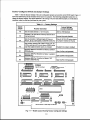

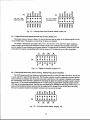


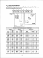
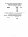
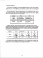


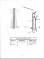


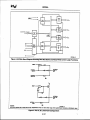
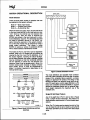

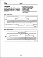

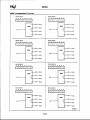
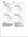
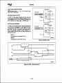
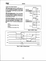
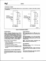
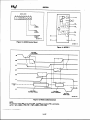


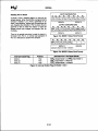

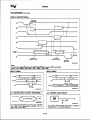


![8月号 [527KB pdfファイル]](http://vs1.manualzilla.com/store/data/006692771_2-8521b451ab07020578c50876c7d28e5d-150x150.png)