1
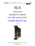
SLS
Multibunch Feedback
Fast ADC and Fast DAC
Setup USER MANUAL
V:1.0
Author: Patrick Pollet, Goran Marinkovic, PSI Dpt. GFA Diagnostic
[email protected]
I. Overview
A. The bunch feedback system parts
•
The position detection part receives the beam signals through pickups and
normalizes them.
•
An ADC is clocked with the machine RF (round 500MHz) and samples the
oscillation of each bunch separately.
•
The digital processing part buffers and calculates the correction signal based on
the ADC sample.
•
A DAC is as well clocked with the machine RF (round 500MHz) and converts the
calculated correction signals back to an analogue value
•
The amplifier scales the correction signals and provides the power to the kicker to
generate the fields in order to correct (damp) the bunch oscillation.
Baseband Signal
(500MHz)
RF
Front End
A/D
Correction Signal
(500MHz)
Digital
Processing
D/A
RF
Amplifier
Wideband
Signal
Hybrid
Network
Pickup
Kicker
Fig. 1 Multibunch feedback system overview.
One of the main problems is a correct setup of the system in order to calculate the
correction signal on basis of the previous samples of the same bunch and to kick this
particular bunch only.
Paul Scherrer Institut • 5232 Villigen PSI
MBFB_ADC_DAC_Setup_User_Manual.doc/ 8/28/07 /page 2 of 12
II. Hardware checks
One of the most important issues to check on the Multi Bunch Feedback system is
the clock. The clock is derived from the machine RF (round 500MHz) and used in the
FPGA to keep track of a particular bunch. Hence loosing the clock means loosing the
information of the bunch number being measured and kicked. This means if the clock
is lost then the ADC card is measuring a particular bunch but the DAC is not kicking
this bunch but a different one.
Therefore check the LEDs on the VME card frontpanel according to following
table.
Please note: The clock lock is as well a part of the alarm handler.
A. ADC LEDs
The ADC VME board has 3 LEDs which visualise the status of
the board. The 3 LEDs are denoted as X, Y and Z.
LED
X
Color
Off
Green
Red
Y
Z
Yellow
Off
green
Red
yellow
Off
green
Red
yellow
X Y Z
Description
Should never happen. Check power or hardware
defect.
The clock system in the FPGA is working properly.
Due to the implementation of the clock system this
indicates that the RF clock jitter is less than 150ps and
no RF clock period was missed.
The clock system in the FPGA is NOT working
properly. Due to the implementation of the clock
system this indicates that the RF clock jitter was/is
bigger than 150ps and/or RF clock period was missed.
Not implemented.
Currently no VME access to this card.
VME signalling access.
VME signalling acknowledge.
Both of the above.
VME Commute directing ADC data to ZBT RAM buffer
and FPDP interface.
VME Commute directing ADC data to FPDP interface
only.
VME Commute directing ZBT RAM buffer data to
FPDP interface (a debugging feature).
VME Commute directing ADC data to ZBT RAM buffer
only.
Paul Scherrer Institut • 5232 Villigen PSI
MBFB_ADC_DAC_Setup_User_Manual.doc/ 8/28/07 /page 3 of 12
B. DAC LEDs
The DAC VME board has 3 LEDs which visualise the status of
the board. The 3 LEDs are denoted as X, Y and Z.
LED
X
Color
off
green
red
Y
Z
yellow
off
green
red
yellow
off
green
red
yellow
X Y Z
Description
Should never happen. Check power or hardware
defect.
The clock system in the FPGA is working properly.
Due to the implementation of the clock system this
indicates that the RF clock jitter is less than 150ps and
no RF clock period was missed.
The clock system in the FPGA is NOT working
properly. Due to the implementation of the clock
system this indicates that the RF clock jitter was/is
bigger than 150ps and/or RF clock period was missed.
Not implemented.
Currently no VME access to this card.
VME signalling access.
VME signalling acknowledge.
Both of the above.
VME Commute directing FPDP data to ZBT RAM
buffer and DAC.
VME Commute directing FPDP data to DAC only.
VME Commute directing ZBT RAM buffer data to DAC
(a debugging feature).
VME Commute directing FPDP data to ZBT RAM
buffer only.
Paul Scherrer Institut • 5232 Villigen PSI
MBFB_ADC_DAC_Setup_User_Manual.doc/ 8/28/07 /page 4 of 12
III.
Restore last stable settings
1.) Open one of the Multibunch-Feedback medm applications.
Fig. 2 Horizontal MBFB medm application
2.) Press the exclamation mark next to “casr all planes”.
Fig. 3 Channel Access Save Restore application
Paul Scherrer Institut • 5232 Villigen PSI
MBFB_ADC_DAC_Setup_User_Manual.doc/ 8/28/07 /page 5 of 12
3.) Select the needed file (probably the newest one).
4.) Press Restore.
Caution: You are restoring all three planes. The saveres file contains not only
the EPICS channels of this particular plane but of horizontal, vertical and
longitudinal plane.
Caution: The “ADC-DAC delay [bucket]” and the clock shifter channels for
ADC, DAC and MOD are not saved and restored.
The button “Info” of the Channel-Access-Save-Restore shows the difference between
the stored and current set EPICs channels.
Paul Scherrer Institut • 5232 Villigen PSI
MBFB_ADC_DAC_Setup_User_Manual.doc/ 8/28/07 /page 6 of 12
IV.
Calculate the FIR values
A. Setup Longitundinal Multibunch Feedback
5.) Open a terminal and change the directory:
cd /exchange/home/dehler/public/MBF/PUL
6.) Check the content of the 00Settings file:
tail 00Settings
7.) Open octave and copy the desired filter:
octave.bin:1>mbf_setfilter(mbf_alltap(1.8e-3, 3.5e-3, 120,0))
This octave script will set the FIR coefficients for the longitudinal MBFB.
Fig. 4 Longitudinal MBFB
Paul Scherrer Institut • 5232 Villigen PSI
MBFB_ADC_DAC_Setup_User_Manual.doc/ 8/28/07 /page 7 of 12
8.) Set “Command” to initialisation and press the “Cmd request” button.
The lonigudinal crate is now set up and running.
There are additional tests in order to see wether the VME cards have synchronized
properly.
Open a rmc terminal for ARIDI-VME-MBFS and type the commands adc_status(1)
and dac_status(2):
ARIDI-VME-MBFS > adc_status(1)
***************************************
***
A D C PU_ADC
***************************************
ADC status...
ADC firmware revision: adc0102
ADC status:
200003
ADC status register:
125 MHz clock lock: 1
DVALID:
1 Reset flag:
0
The important information here is that the “125 MHz clock lock” is “1”. This means
that the clock was correctly received since the initialisation of the card. The meaning
if “DVALID” is “1” is that the FPGA retrieves bunch information from the ADC, the
calculation pipeline was started and the correction data was send to the DAC.
ARIDI-VME-MBFS > dac_status(2)
***************************************
***
D A C PU_DAC
***************************************
DAC status...
DAC firmware revision: dac0100
DAC status:
2210003
DAC status bits:
Clock lock:
1
DAC start
1
DVALID
1
FIFO empty
0 FIFO Half full
FIFO full
0 FIFO overflow
Acq enable
1
Commute
0
Run mode
0
1
0
The important information here is that the “Clock lock” is ”1”. This means that the
clock was correctly received since the initialisation of the card. The meaning of
“DVALID” is “1” means that the FPGA receives the correction data from the ADC. If
“DAC start” is “1” then the start pulse was received from the ADC. If “FIFO Half
full” is “1” then this means that the FPGA buffer contains valid correction data and
operates in a valid range (e.g. did not overflow or underflow).
Paul Scherrer Institut • 5232 Villigen PSI
MBFB_ADC_DAC_Setup_User_Manual.doc/ 8/28/07 /page 8 of 12
B. Setup Horizontal Multibunch Feedback
1.) Open a terminal and change the directory:
cd /exchange/home/dehler/public/MBF/PUH
2.) Check the content of the 00Settings file:
tail 00Settings
3.) Open octave and copy the desired filter:
octave.bin:1>mbf_alltap(.431,340)
This octave script will set the FIR coefficients for the horizontal MBFB.
Fig. 5 Horizontal MBFB
4.) Set “Command” to initialisation and press the “Cmd request” button.
The horizontal crate is now set up and running.
There are additional tests in order to see wether the VME cards have synchronized
properly.
Paul Scherrer Institut • 5232 Villigen PSI
MBFB_ADC_DAC_Setup_User_Manual.doc/ 8/28/07 /page 9 of 12
Open a rmc terminal for ARIDI-VME-MBFX and type the commands adc_status(0)
and dac_status(1):
ARIDI-VME-MBFX > adc_status(0)
***************************************
***
A D C PUH_ADC
***************************************
ADC status...
ADC firmware revision: adc0207
ADC status:
200003
ADC status register:
125 MHz clock lock: 1
DVALID:
1 Reset flag:
0
The important information here is that the “125 MHz clock lock” is “1”. This means
that the clock was correctly received since the initialisation of the card. The meaning
if “DVALID” is “1” is that the FPGA retrieves bunch information from the ADC, the
calculation pipeline was started and the correction data was send to the DAC.
ARIDI-VME-MBFX > dac_status(1)
***************************************
***
D A C PUH_DAC
***************************************
DAC status...
DAC firmware revision: dac0100
DAC status:
2210003
DAC status bits:
Clock lock:
1
DAC start
1
DVALID
1
FIFO empty
0 FIFO Half full
FIFO full
0 FIFO overflow
Acq enable
1
Commute
0
Run mode
0
1
0
The important information here is that the “Clock lock” is “1”. This means that the
clock was correctly received since the initialisation of the card. The meaning of
“DVALID” is “1” means that the FPGA receives the correction data from the ADC. If
“DAC start” is “1” then the start pulse was received from the ADC. If “FIFO Half
full” is “1” then this means that the FPGA buffer contains valid correction data and
operates in a valid range (e.g. did not overflow or underflow).
C. Setup Vertical Multibunch Feedback
1.) Open a terminal and change the directory:
cd /exchange/home/dehler/public/MBF/PUV
2.) Check the content of the 00Settings file:
Paul Scherrer Institut • 5232 Villigen PSI
MBFB_ADC_DAC_Setup_User_Manual.doc/ 8/28/07 /page 10 of 12
tail 00Settings
3.) Open octave and copy the desired filter:
octave.bin:1>mbf_alltap(.27,70)
This octave script will set the FIR coefficients for the vertical MBFB.
Fig. 6 Vertical MBFB
4.) Set “Command” to initialisation and press the “Cmd request” button.
The vertical crate is now set up and running.
There are additional tests in order to see wether the VME cards have synchronized
properly.
Open a rmc terminal for ARIDI-VME-MBFY and type the commands adc_status(2)
and dac_status(3):
ARIDI-VME-MBFY > adc_status(2)
***************************************
***
A D C PUV_ADC
***************************************
ADC status...
Paul Scherrer Institut • 5232 Villigen PSI
MBFB_ADC_DAC_Setup_User_Manual.doc/ 8/28/07 /page 11 of 12
ADC firmware revision: adc0207
ADC status:
200003
ADC status register:
125 MHz clock lock: 1
DVALID:
1 Reset flag:
0
The important information here is that the “125 MHz clock lock” is “1”. This means
that the clock was correctly received since the initialisation of the card. The meaning
if “DVALID” is “1” is that the FPGA retrieves bunch information from the ADC, the
calculation pipeline was started and the correction data was send to the DAC.
ARIDI-VME-MBFY > dac_status(3)
***************************************
***
D A C PUV_DAC
***************************************
DAC status...
DAC firmware revision: dac0100
DAC status:
2210003
DAC status bits:
Clock lock:
1
DAC start
1
DVALID
1
FIFO empty
0 FIFO Half full
FIFO full
0 FIFO overflow
Acq enable
1
Commute
0
Run mode
0
1
0
The important information here is that the “Clock lock” is “1”. This means that the
clock was correctly received since the initialisation of the card. The meaning of
“DVALID” is “1” means that the FPGA receives the correction data from the ADC. If
“DAC start” is “1” then the start pulse was received from the ADC. If “FIFO Half
full” is “1” then this means that the FPGA buffer contains valid correction data and
operates in a valid range (e.g. did not overflow or underflow).
Paul Scherrer Institut • 5232 Villigen PSI
MBFB_ADC_DAC_Setup_User_Manual.doc/ 8/28/07 /page 12 of 12