1
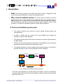
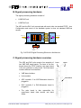
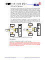
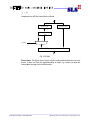
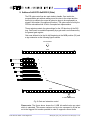
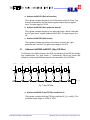
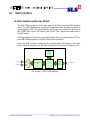
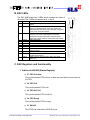
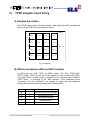
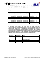
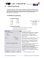
SLS
Transversal
Multibunch Feedback
Fast ADC and Fast DAC
USER MANUAL
V:1.0
Author: Patrick Pollet, Goran Marinkovic, PSI Dpt. GFA Diagnostic
[email protected]
I. Generalities
•
Goal: The synchrotron beam at the Swiss Light Source (SLS) in Villigen-PSI needs
to be monitored and stabilized to achieve its rated performance.
•
Why a bunch feedback system: An electron beam circulating in a ring at
speed close to that of light excites electro-magnetical fields; this em-field energy is
deposed locally for a certain amount of time around the whole accelerator structure.
This stored energy may cause unwanted transversal beam oscillation under certain
conditions. The task of the feedback system is to damp these oscillations.
A. The bunch feedback system parts
•
The position detection part receives the beam signals through pickups and
normalizes them.
•
An ADC is clocked with the machine RF (round 500MHz) and samples the
oscillation of each bunch separately.
•
The digital processing part buffers and calculates the correction signal based on
the ADC sample.
•
A DAC is as well clocked with the machine RF (round 500MHz) and converts the
calculated correction signals back to an analogue value
•
The amplifier scales the correction signals and provides the power to the kicker to
generate the fields in order to correct (damp) the bunch oscillation.
Baseband Signal
(500MHz)
RF
Front End
A/D
Correction Signal
(500MHz)
Digital
Processing
D/A
RF
Amplifier
Wideband
Signal
Hybrid
Network
Pickup
Kicker
Fig. 1 Multibunch feedback system overview.
One of the main problems is a correct setup of the system in order to calculate the
correction signal on basis of the previous samples of the same bunch and to kick this
particular bunch only.
Paul Scherrer Institut • 5232 Villigen PSI
MBFB_ADC_DAC_User_Manual.doc/ 12/13/06 /page 2 of 27
B. Signal processing hardware
The signal processing hardware consists of:
•
1 VME ADC unit.
•
1 VME DAC unit.
The ADC and the DAC unit communicate with each other via standard FPDP – bus.
Configuration and control of the feedback system is done via standard VME-bus
access.
Clock
DAC Board
Commute
Gain
FPDP
FIR
A/D
FPDP
IIR
Analogue IN
Grey to Binary
ADC Board
M
U
X
FPDP
FPDP
M
U
X
Analogue OUT
D/A
FPDP
Start ADC
FPDP
Start DAC Clock
Clock Distribution
External
External
Clock Shift
Clock
Setting
Fig. 2 ADC-DAC Digital Processing Electronics Architecture.
C. Signal processing hardware overview
The ADC and DAC units consist of an assembly of
two VME 6HE sized boards. The lower of the two
boards drives the FPDP interface, the upper board
is the unit controller or main board. The main board
contains different functionalities:
•
VME slave interface.
•
Unit controller.
•
ADC controller if an ADC-Mezzanine board is
plugged in.
•
DAC controller if a DAC-Mezzanine board is
plugged in.
•
The main board is also responsible for
upper/lower board data transfer and hand
shake.
Paul Scherrer Institut • 5232 Villigen PSI
lower
upper
mezzanine
MBFB_ADC_DAC_User_Manual.doc/ 12/13/06 /page 3 of 27
1. ADC and DAC Mainboard
According to the block diagram below, the mainboard allows various data flows.
The data flow within the board is controlled by means of the FPGA (XILINX™
XC2V1000-6-FG456C) firmware. The data flow controls the interaction between
VME bus access, a fast buffer (ZBT RAM), the ADC/DAC and the FPDP
interface. The ADC and DAC board contains a fast RAM buffer denoted as ZBT
RAM, which stores the ADC samples and the DAC values consistently in a ring
buffer. The buffer is constructed such that at each address the bunch with the
same number is stored, hence giving a good possibility to observe a particular
bunch. This ring buffer is needed primarily for setting up the system and
observing the beam movement at runtime of the MBFB.
The mainboard hardware configuration is almost (one exception is the
terminating resistors on the main board) the same for the ADC and the DAC
board, only the type of mezzanine (ADC or DAC) and the FPGA firmware are
distinguishing between the functionality of the two units.
VME Bus Interface
VME Bus Interface
Address32 &
Control
5V TTL &
Data32
LVDS
@125MHz
Clock &
Control
LVDS
ADC
Mezanine
Address20 &
Control
LVTTL
Data32
LVDS
@125MHz
Clock &
Control
LVDS
DAC
Mezanine
FPDP
Board
Connector
Xilinx
Virtex II FPGA
Data8
LVDS DDR
@250MHz
Data32
TTL
@40MHz
Address32 &
Control
5V TTL &
Data32
TTL
@40MHz
Data16
LVDS
@250MHz
Address &
Control
LVDS
Address20 &
Control
LVTTL
Data32
LVTTL
@125MHz
possible
data flow
directions
ZBT-RAM
FPDP
Board
Connector
Xilinx
Virtex II FPGA
Address &
Control
LVDS
Data32
LVTTL
@125MHz
ZBT-RAM
possible
data flow
directions
Fig. 3 Possible data flow in the ADC and DAC board.
FPGA Dataflow
The FPGA is configured either as ADC or as DAC controller.
Please note: It is strictly forbidden to swap the mezzanine boards without
clearing first the FPGA firmware. If a board with an unknown firmware is used
then the first thing to do is to clear the content of the configuration EPROM
by means of the XILINX® Impact tool.
Paul Scherrer Institut • 5232 Villigen PSI
MBFB_ADC_DAC_User_Manual.doc/ 12/13/06 /page 4 of 27
II. ADC Interface
A. ADC Dataflow within the FPGA
The incoming analogue signal is sampled at a rate of 500 MHz. Once enabled, the
ADC outputs a 500 MSamples/s, 8 Bit LVDS differential DDR data bus with a
synchronous LVDS clock at 250 MHz. The 8 bit data is then demultiplexed (1 to 4
DEMUX) to produce a 32 bit wide FPGA internal data bus at 125 MHz. This bus
passes to a Gray to Binary decoder, an IIR filter, an 8tap FIR filter, a bunch gain
control, a 2 way data redirector (commute) and finaly the FPDP interface. This data
redirector may send the data either differentially to the FPDP-demux daughter board
or to the ZBT RAM ring buffer or to both of them at the same time. The output
dataflow is synchronous with the reference clock (250 MHz).
Interface
to
ZBT RAM
Gray2Bin
ADCData(8)
D
E
M
U
X
IIR
8tap FIR
Gain
32
8
8
8
8
8
8
8
8
8
8
Commute
8
8
8
8
8
8
8
8
8
8
32
Interface
to
FPDP
Board
FPDPData(32)
Fig. 4 ADC-FPDP Dataflow
Paul Scherrer Institut • 5232 Villigen PSI
MBFB_ADC_DAC_User_Manual.doc/ 12/13/06 /page 5 of 27
B. ADC LEDs
The ADC VME board has 3 LEDs which visualise the status of
the board. The 3 LEDs are denoted as X, Y and Z.
LED
X
Color
off
green
red
Y
Z
yellow
off
green
red
yellow
off
green
red
yellow
X Y Z
Description
Should never happen. Check power or hardware
defect.
The clock system in the FPGA is working properly.
Due to the implementation of the clock system this
indicates that the RF clock jitter is less than 150ps and
no RF clock period was missed.
The clock system in the FPGA is NOT working
properly. Due to the implementation of the clock
system this indicates that the RF clock jitter was/is
bigger than 150ps and/or RF clock period was missed.
Not implemented.
Currently no VME access to this card.
VME signalling access.
VME signalling acknowledge.
Both of the above.
VME Commute directing ADC data to ZBT RAM buffer
and FPDP interface.
VME Commute directing ADC data to FPDP interface
only.
VME Commute directing ZBT RAM buffer data to
FPDP interface (a debugging feature).
VME Commute directing ADC data to ZBT RAM buffer
only.
C. Registers and functionality
1. Address 0x000000 (Status Register)
a) 21: DVALID
The FPDP bus transmits the DVALID bit set.
b) 0: 125 MHz Clock Lock
This bit is set if the clocks are working according to the specs of the DCM
(Digital Clock Manager) inside the FPGA. For more information on the
DCM please refer to the XILINX datasheet of the VirtexII FPGA.
2. Address 0x000010 (Control Register)
a) 31:Board Reset
A write access at this bit causes:
o Stop of any running acquisition.
o Reset the FPDP interface.
Paul Scherrer Institut • 5232 Villigen PSI
MBFB_ADC_DAC_User_Manual.doc/ 12/13/06 /page 6 of 27
o Reset all registers to their default values.
o Set all memory pointers to their base address.
o Reinitialization of the board hardware.
b) 21…20: Run Mode Select
o 00: External Trigger mode. The acquisition is started by the FPGA
internal timer.
o 01: Software trigger mode. The acquisition is started internally by
Software trigger.
o 10: no action
o 11: no action
c) 12: FPDP Reset
Setting this bit will reset the FPDP address counter and the FPDP strobes
signals. After “Board Reset” this bit is set to 1, therefore the FPDP is
driven into its initial stage and waits for the start signal (DVALID).
d) 5…4: Commute
Controlls the dataflow in the FPGA.
o 00: ADC data to FPDP and to ZBT RAM
o 01: ADC data to FPDP only
o 10: ZBT RAM data to FPDP
o 11: ADC data to ZBT RAM only
e) 0: Acq Enable
Setting this bit will enable the clock on the ADC mezanine board.
3. Address 0x000020 (Firmware Version)
This register holds the actual firmware version number for verification purposes
o [27..24] : Hexadecimal “A”
o [23..20] : Hexadecimal “D”
o [19..16] : Hexadecimal “C”
o [15…0] Firmware Version Nr (4x Hex Number)
Paul Scherrer Institut • 5232 Villigen PSI
MBFB_ADC_DAC_User_Manual.doc/ 12/13/06 /page 7 of 27
4. Address 0x000040 (ZBT RAM Stop Address)
During acquisition, this register contains the last written RAM address. The last
address will be kept until a new acquisition cycle is started.
Please note: Although the last written RAM address is stored, the main
address counter is updated internally and hence starts writing the ring buffer at
the correct position for the actual bunch number.
5. Address 0x000110 (ZBT RAM Last Address)
The last ZBT RAM address (max usable size) of the used memory should be
adjusted to an integer multiple of the complete bunch turns to be stored in
memory. If the RAM size is set with a value which is not an integer multiple of
complete bunch turns, then a “data jump” at the end of the buffer memory is
caused. Which means: The same memory position (address) is not storing the
information of the same bunch number but of different bunches. E.g the bunch
with a specific number is not stored at the same address when the ZBT RAM
buffer is filled.
An example for setting the correct value:
Nr. of bunches per turn = 480
Nr. of bunches stored with each address = 4 (data organisation of the ZBT)
Size of memory = 4194304 Bytes (organized as 1048576 x 32bit => 4
samples/address)
Last memory address = (4194304 / 480) * (480 / 4) - 1 = 1048559 = 0xFFFEF
6. Address 0x000120 (ADC Clock Phase Timing Settings)
This register contains the ADC clock phase timing for sampling the ADC data at
rising and falling clock edges.
Please note: The base for the rising edge clock is the 250 MHz reference clock
and the base for the falling edge timing is the rising edge clock. This means if
you are modifying the rising edge timing, then the falling edge timing is modified
as well! The default values set in this register are evaluated by means of
measurement and work nicely for the given boards. Modify these registers only
with care.
a) 31..24: Timing of ADC Clock Falling Edge
A write access at this address moves the sampling point of the ADC read
at the falling edge of the 250 MHz adc clock. The sampling point is
calculated as follows:
sampling_falling_edge = sampling_falling_edge_value*(2ns/256)
Paul Scherrer Institut • 5232 Villigen PSI
MBFB_ADC_DAC_User_Manual.doc/ 12/13/06 /page 8 of 27
Sampling_falling_edge = delay between rising edge of the sample clock to
the falling edge of the sampling clock. This value is used for the DCM
(Digital Clock Manager) inside the FPGA, for more information on the
DCM please refer to the XILINX datasheet of the VirtexII FPGA.
b) 16..23: Timing of ADC Rising Edge
A write access at this address moves the sampling point of the ADC read
in contrast to the rising edge of the 250MHz reference clock. The sampling
point is calculated as follows:
sampling_rising_edge = sampling_rising_edge_value*(2ns/256)
Sampling_rising_edge = delay between rising edge of the sampling clock
to the rising edge of the reference clock. This value is used for the DCM
(Digital Clock Manager) inside the FPGA, for more information on the
DCM please refer to the XILINX datasheet of the VirtexII FPGA
7. Address 0x000130-0x000140 (ADC Start Timing Setting)
This register contains the ADC and DAC start timing setting. The ADC is started
when the delay timer is started (“Bunch delay trigger”) and after a
programmable delay (“Bunch delay”) a start signal for the DAC card is
generated. E.g. the delay for the ADC to DAC start is defined and triggered by
these registers here.
a) Address 0x000130 (Bunch delay trigger)
If bit 0 is set set (to ‘1’), then the internal timer is loaded with the value
stored in the “Bunch delay” register (address 0x000140) and started in
order to trigger the DAC start. If bit 0 is reset (to ‘0’) then the internal timer
is reloaded and waits to be triggered again to start the DAC.
b) Address 0x000140 (Bunch delay).
This register contains the bunch delay in 2ns steps. The delay value range
is 0 to 16384. The delay is calculated as follows:
delay = (delay _ value + 1) * 2ns
8. Address 0x000190 (ADC Enable IIR Filter Setting)
This register contains the enable signal for IIR filtering in the ADC. If bit 0 is set
(to ‘1’), then the IIR filter is enabled. If the IIR filter is enabled then following
formula is used for each bunch sample separately with a resolution of 2 −20 :
7
y n = ( y n −.1 + x n ) − 8 x n
8
If IIR is disabled (to ‘0’) then the formula is simply:
Paul Scherrer Institut • 5232 Villigen PSI
MBFB_ADC_DAC_User_Manual.doc/ 12/13/06 /page 9 of 27
y n = −8 x n
Graphically the IIR filter looks like the follows.
8
y(n)=x(n) * 2^20
y(n)=x(n) * 2^23
32
16
y(n)=7/8 * y(n-1) + x(n)
32
0
iir_enable
0
1
16
16
Fig. 5 IIR filter
Please note: The figure above shows only the mathematical behaviour for each
bunch, it does not show the implementation in detail, e.g it does not show the
intermediate storage for the 480 bunches.
Paul Scherrer Institut • 5232 Villigen PSI
MBFB_ADC_DAC_User_Manual.doc/ 12/13/06 /page 10 of 27
9. Address 0x0001C0-0x0001E0 (Gain)
The FIR gain control has two main tasks to handle. One task is the
programmable gain without adding more bit-noise to the output and the
second is to saturate the output at gains too large to be expressed in a
signed 8 bit number (2complement number). The gain control is fed by the
FIR filter calculation with 36 bit in 2complement representation.
These registers contain the gain settings for the 479 bunches of the SLS
ring. One bunch is controlled separately by a gain and is not influenced by
the general gain register.
Gain was defined to be the bit shift beginning at the MSB position (35) and
a sign extension as the following figures shows.
FIR calculation
35 bit
34
0
8 bit
34
34 34
0
0
9 bit
34
34 34
1
0
10 bit
34
34 34
2
0
11 bit
34
34 34
3
0
12 bit
34
34 34
4
0
13 bit
34
34 34
0
5
35 bit
34
0
27
8 LSB bit scaled value
Fig. 6 Gain and saturation control
Please note: The figure above shows the 8 LSB bit scalled value as output
which is saturated. This means numbers too big to be expressed in 8 bits are
set to the biggest 8 bit number possible in order to suppress rollover faults.
Paul Scherrer Institut • 5232 Villigen PSI
MBFB_ADC_DAC_User_Manual.doc/ 12/13/06 /page 11 of 27
a) Address 0x0001C0 (Gain all bunches)
This register contains the gain for the 479 bunches of the SLS ring. One
bunch is controlled by the gain bunch register and not by this register
here. The gain range is 0 to 26.
b) Address 0x0001D0 (Gain particular bunch).
This register contains the gain of one particular bunch, which is selected
by the “gain bunch” register (address 0x0001E0). The gain range is 0 to
26.
c) Address 0x0001E0 (Gain bunch).
This register contains the number of the bunch for which the “gain
particular gain” is active. The gain bunch range is 0 to 479.
10.
Address 0x000200-0x000270 (8tap FIR filter)
For filtering of the 480 bunches in the SLS ring following 8 tap FIR filter design
was implemented. For each bunch z-7 successively values are stored and
shifted in a dual ported RAM and used for the calculation of the FIR filter.
i_fir_coef(1)
i_fir_coef(0)
Z-1
i_fir_in
i_fir_coef(2)
Z-1
i_fir_coef(3)
Z-1
i_fir_coef(4)
Z-1
i_fir_coef(5)
Z-1
i_fir_coef(6)
Z-1
i_fir_coef(7)
Z-1
X
X
X
X
X
X
X
X
Saturation
control
0
o_fir_out
Fig. 7 8tap FIR filter
a) Address 0x000200 (8 tap FIR filter coefficient 0)
This register contains the 8 tap FIR filter coefficient 0 (i_fir_coef(0)). The
coefficient value range is -32768 to 32767.
Paul Scherrer Institut • 5232 Villigen PSI
MBFB_ADC_DAC_User_Manual.doc/ 12/13/06 /page 12 of 27
b) Address 0x000210 (8 tap FIR filter coefficient 1)
This register contains the 8 tap FIR filter coefficient 1 (i_fir_coef(1)). The
coefficient value range is -32768 to 32767.
c) Address 0x000220 (8 tap FIR filter coefficient 2)
This register contains the 8 tap FIR filter coefficient 2 (i_fir_coef(2)). The
coefficient value range is -32768 to 32767.
d) Address 0x000230 (8 tap FIR filter coefficient 3)
This register contains the 8 tap FIR filter coefficient 3 (i_fir_coef(3)). The
coefficient value range is -32768 to 32767.
e) Address 0x000240 (8 tap FIR filter coefficient 4)
This register contains the 8 tap FIR filter coefficient 4 (i_fir_coef(4)). The
coefficient value range is -32768 to 32767.
f) Address 0x000250 (8 tap FIR filter coefficient 5)
This register contains the 8 tap FIR filter coefficient 5 (i_fir_coef(5)). The
coefficient value range is -32768 to 32767.
g) Address 0x000260 (8 tap FIR filter coefficient 6)
This register contains the 8 tap FIR filter coefficient 6 (i_fir_coef(6)). The
coefficient value range is -32768 to 32767.
h) Address 0x000270 (8 tap FIR filter coefficient 7)
This register contains the 8 tap FIR filter coefficient 7 (i_fir_coef(7)). The
coefficient value range is -32768 to 32767.
Paul Scherrer Institut • 5232 Villigen PSI
MBFB_ADC_DAC_User_Manual.doc/ 12/13/06 /page 13 of 27
III.
DAC Interface
A. DAC dataflow within the FPGA.
The DAC FPGA receives a 32 bit data word at 125 MHz from the FPDP daughter
board. The FPDP data passes a redirector (Commute) before the data is stored in a
synchronization FIFO. The synchronization FIFO read out is started at detection of
the “START DAC” signal. The origin of this “START DAC” signal is the delay timer of
the ADC board.
The data redirector (Commute) may send the data either the synchronization FIFO or
to the ZBT RAM ring buffer or to both of them at the same time.
Finally the DAC interface multiplexes the synchronization FIFO data to the output
ports A and B at a frequency of 250 MHz synchronously to the DAC reference clock.
Interface
to
ZBT RAM
32
DACDataA(8)
DACDataB(8)
M
U
X
32
Synchronization
FIFO
32
Commute
32
Interface
to
FPDP
Board
FPDPData(32)
Fig. 8 FPDP – DAC FPGA data flow
Paul Scherrer Institut • 5232 Villigen PSI
MBFB_ADC_DAC_User_Manual.doc/ 12/13/06 /page 14 of 27
B. DAC LEDs
The DAC VME board has 3 LEDs which visualise the status of
the board. The 3 LEDs are denoted as X, Y and Z.
LED
X
Color
off
green
red
Y
Z
yellow
off
green
red
yellow
off
green
red
yellow
X Y Z
Description
Should never happen. Check power or hardware
defect.
The clock system in the FPGA is working properly.
Due to the implementation of the clock system this
indicates that the RF clock jitter is less than 150ps and
no RF clock period was missed.
The clock system in the FPGA is NOT working
properly. Due to the implementation of the clock
system this indicates that the RF clock jitter was/is
bigger than 150ps and/or RF clock period was missed.
Not implemented.
Currently no VME access to this card.
VME signalling access.
VME signalling acknowledge.
Both of the above.
VME Commute directing FPDP data to ZBT RAM
buffer and DAC.
VME Commute directing FPDP data to DAC only.
VME Commute directing ZBT RAM buffer data to DAC
(a debugging feature).
VME Commute directing FPDP data to ZBT RAM
buffer only.
C. DAC Registers and functionality
1. Address 0x000000 (Status Register)
a) 27: FIFO Overflow
The synchronization FIFO overrun or data was read before it was stored in
the FIFO.
b) 26: FIFO Full
The synchronization FIFO is full.
c) 25: FIFO Half Full
The synchronization FIFO is half full.
d) 24: FIFO Empty
The synchronization FIFO is empty.
e) 21: DVALID
The FPDP bus received the DVALID bit set.
Paul Scherrer Institut • 5232 Villigen PSI
MBFB_ADC_DAC_User_Manual.doc/ 12/13/06 /page 15 of 27
f) 16: START DAC
Start for reading the synchronization FIFO detected. The origin of this
“START DAC” signal is the delay timer of the ADC board.
g) 0: 250 MHz Clock Lock
This bit is set if the clocks are working according to the specs of the DCM
(Digital Clock Manager) inside the FPGA. For more information on the
DCM please refer to the XILINX datasheet of the VirtexII FPGA.
2. Address 0x000010 (Control Register)
a) 31: Board Reset
o Stop any running acquisition
o Reset the FPDP interface.
o Reset all registers to their default values
o Set all memory pointers to their base address
o Reinitialize board hardware
b) 21…20: Run Mode select
o 00: External trigger mode. The acquisition is started by external event
“START DAC”.
o 01: Software trigger mode. The acquisition is started internally by
Software trigger.
o 10: no action
o 11: no action
c) 12: FPDP Reset
Setting this bit will reset the FPDP bus interface. After “Board Reset” this
bit is set (to ‘1’), therefore the FPDP is driven into its initial stage and waits
for the start signal.
d) 5…4: Commute
o 00: FPDP data to DAC and to ZBT RAM
o 01: FPDP data to DAC only
o 10: ZBT RAM data to DAC
o 11: FPDP data to ZBT RAM only
Paul Scherrer Institut • 5232 Villigen PSI
MBFB_ADC_DAC_User_Manual.doc/ 12/13/06 /page 16 of 27
e) 0: Acq Enable
Setting this bit will enable the DAC to receive start signals. Disabling this
bit, stops the acquisition.
3. Address 0x000020 (Firmware Version)
This register holds the actual firmware version number for verification purposes
o [27…24] : Hexadecimal “D”
o [23…20] : Hexadecimal “A”
o [19…16] : Hexadecimal “C”
o [15…0] Firmware Version Nr (4x Hex Number)
4. Address 0x000040 (ZBT RAM Stop Address)
During acquisition, this register contains the last written RAM address. The last
address will be kept until a new acquisition cycle is started.
Please note: Although the last written RAM address is stored, the main
address counter is updated internally and hence starts writing the ring buffer at
the correct position for the actual bunch number.
5. Address 0x000110 (ZBT RAM Last Address)
The last ZBT RAM address (max usable size) of the used memory should be
adjusted to an integer multiple of the complete bunch turns to be stored in
memory. If the RAM size is set with a value which is not an integer multiple of
complete bunch turns, then a “data jump” at the end of the buffer memory is
caused. The same memory position (address) is not storing the information of
the same bunch but by different bunches. E.g the bunch with a specific number
is not stored at the same address when the ZBT RAM buffer is filled.
An example for setting the correct value:
Nr. of bunches per turn = 480
Nr. of bunches stored with each address = 4 (data organisation of the ZBT)
Size of memory = 4194304 Bytes (organized as 1048576 x 32bit => 4
samples/address)
Last memory address = (4194304 / 480) * (480 / 4) - 1 = 1048559 = 0xFFFEF
Paul Scherrer Institut • 5232 Villigen PSI
MBFB_ADC_DAC_User_Manual.doc/ 12/13/06 /page 17 of 27
IV.
FPDP daughter board timing
A. Samples description
Each FPDP word is made of four 8 bit samples. After starting the ADC acquisition the
data out of the FPDP ports are ordered as shown.
FPDP #1
FPDP #2
FPDP #3
FPDP #4
Sample 1
Sample 5
Sample 9
Sample 13
Sample 2
Sample 6
Sample 10
Sample 14
Sample 3
Sample 7
Sample 11
Sample 15
Sample 4
Sample 8
Sample 12
Sample 16
bit 31
bit 24
bit 23
bit 16
bit 15
bit 8
bit 7
bit 0
Fig. 9 Samples
B. Differences between ADC and DAC transfers
In ADC-mode, the ADC FPGA is FPDP master. The lines “FPDP_Data”,
“FPDP_DValid”, “FPDP_Strobe” and “FPDP_Address” are driven by the ADC FPGA.
The signal “MCLK” (master clock) is derived from the reference clock (250MHz).
“FPDP Reset”, is controlled by the VME interface. Three additional signals,
“Commute[1…0]” and “AcqEnable”, are needed to enable the data redirection
through the commute element according to the following table:
Commute
ACQEnable
Legend
00
1
ADC Data to FPDP and to ZBT RAM
01
1
ADC Data to FPDP only
10
1
ZBT RAM Data to FPDP
11
1
ZBT RAM to ADC
xx
0
No acquisition
Paul Scherrer Institut • 5232 Villigen PSI
MBFB_ADC_DAC_User_Manual.doc/ 12/13/06 /page 18 of 27
The “FPDP_Address” is set by an internal modulo 6 counter. The count width is given
by the signals “VMEFPDPAddress[3…0]”. This counter is reset at initialization and
delivered in parallel with the data to the FPDP interface.
Example:
Sample
FPDPData[7:0]
FPDPData[15:8]
FPDPData[23:16]
FPDPData[31:24]
FPDP
Address
0
ADCData(n+3)
ADCData(n+2)
ADCData(n+1)
ADCData(n)
0
1
ADCData(n+7)
ADCData(n+6)
ADCData(n+5)
ADCData(n+4)
1
…
…
…
…
…
…
5
ADCData(n+23)
ADCData(n+22)
ADCData(n+21)
ADCData(n+20)
5
6
ADCData(n+27)
ADCData(n+26)
ADCData(n+25)
ADCData(n+24)
0
7
ADCData(n+31)
ADCData(n+30)
ADCData(n+29)
ADCData(n+28)
1
…
…
…
…
…
…
In DAC-mode, DAC FPGA is the FPDP slave. The lines “FPDP_Data”,
“FPDP_DValid” and “FPDP_Strobe” are driven by the FPDP-daughter board. The
signal “MCLK” (master clock) is derived from the reference clock (250MHz).
“FPDP_Reset” is controlled by the VME interface. “FPDP_Sync” can be used to
resynchronize data in this working mode and should not be used at the moment. Two
additional signals, “Commute[1…0]” and “AcqEnable”, are needed to enable the data
redirection through the commute element according to the following table:
VMECommute
VMEAcqEnable
Legend
00
1
FPDP Data to DAC and to ZBT RAM
01
1
FPDP Data to DAC only
10
1
ZBT RAM Data to DAC
11
1
FPDP Data to ZBT RAM
xx
0
No Acquisition
Paul Scherrer Institut • 5232 Villigen PSI
MBFB_ADC_DAC_User_Manual.doc/ 12/13/06 /page 19 of 27
V. VME Interface
A. Setting the VME Board Base Address
Using a VME 64x crate, the board base address is set according to the slot
geographical address map. The VME address switch SW2 should be disabled (all
switch in position off) to assure a correct address decoding. Any 5 consecutive
address lines range can be used (A31..A27; A27..A22 etc…) for the board address
mapping, giving a maximal address space of 128 MByte per VME slot if using the 5
upper address lines (A31.. A27). The decoded address lines are selected by the
rotating hex coder switch SW3.
SW3
0
1
2
3
4
5
6
7..F
Address lines decoded
A31…A27
A30…A26
A29…A25
A28…A24
A27…A23
A26…A22
A25…A21
Not available
Address space
128 MByte
64 MByte
32 MByte
16 MByte
8 MByte
4 MByte
2 MByte
B. Board base address adjustment
On normal VME64x crates the adjustment can only be set by choice of the correct
slot and by use of the switch SW3. On crates where geographical addressing is not
available, the geographical addresses should be set manually, using switch SW2.
SLOT
1
2
3
4
5
6
7
8
9
10
11
12
13
14
15
16
17
GA_Lines
00001
00010
00011
00100
00101
00110
00111
01000
01001
01010
01011
01100
01101
01110
01111
10000
10001
0
08000000
10000000
18000000
20000000
28000000
30000000
38000000
40000000
48000000
50000000
58000000
60000000
68000000
70000000
78000000
80000000
88000000
Paul Scherrer Institut • 5232 Villigen PSI
1
04000000
08000000
0c000000
10000000
14000000
18000000
1c000000
20000000
24000000
28000000
2c000000
30000000
34000000
38000000
3c000000
40000000
44000000
2
02000000
04000000
06000000
08000000
0a000000
0c000000
0e000000
10000000
12000000
14000000
16000000
18000000
1a000000
1c000000
1e000000
20000000
22000000
3
01000000
02000000
03000000
04000000
05000000
06000000
07000000
08000000
09000000
0a000000
0b000000
0c000000
0d000000
0e000000
0f000000
10000000
11000000
4
00800000
01000000
01800000
02000000
02800000
03000000
03800000
04000000
04800000
05000000
05800000
06000000
06800000
07000000
07800000
08000000
08800000
5
00400000
00800000
00c00000
01000000
01400000
01800000
01c00000
02000000
02400000
02800000
02c00000
03000000
03400000
03800000
03c00000
04000000
04400000
6
00200000
00400000
00600000
00800000
00a00000
00c00000
00e00000
01000000
01200000
01400000
01600000
01800000
01a00000
01c00000
01e00000
02000000
02200000
MBFB_ADC_DAC_User_Manual.doc/ 12/13/06 /page 20 of 27
18
19
20
21
10010
10011
10100
10101
90000000
98000000
a0000000
a8000000
48000000
4c000000
50000000
54000000
24000000
26000000
28000000
2a000000
12000000
13000000
14000000
15000000
09000000
09800000
0a000000
0a800000
04800000
04c00000
05000000
05400000
02400000
02600000
02800000
02a00000
C. Use of the VME32 crate
The boards are VME32 compatible, but since +3.3V power supply is not available on
VME32 crates, few hardware changes need to be done:
o Mainboard Jumper CB3 should be set.
o FPDP board Jumper JP1 should be set.
Paul Scherrer Institut • 5232 Villigen PSI
MBFB_ADC_DAC_User_Manual.doc/ 12/13/06 /page 21 of 27
VI.
JTAG Programming
For upgrade purposes a JTAG connector is accessible on the ADC and DAC front panel.
This connector accesses only the mainboard FPGA. For upgrading the FPDP-board, the
assembly should be dismounted in order to access the JTAG connector placed at the top
side of the board. The Xilinx programming environment may be downloaded at
http://www.xilinx.com/webpack/
A. ADC/DAC Programming
1. Connector Pinout:
1: TCK
5: TMS
2: GND
9: TDI
3: TDO
10: GND
4: VCC
2. Programming steps
o Copy the ADC or DAC files to a directory on your PC.
o Plug the board in and switch power on.
Connect the JTAG cable.
Start Xilinx Impact program: start => Programs
=> Xilinx ISExy => Accessories => Impact
By the popup menu “Operation Mode
Selection”, choose <Configure Device> and
press <Next>.
By the popup menu “Configure Device”, choose
<Boundary-Scan Mode> and press <Next>.
By the popup menu “Boundary-Scan Mode
Selection”, choose <Automatically connect>
and press <Finish>.
The programs will check the connection and
ask for a configuration file, choose
dac_fpga.mcs or adc_fpga.mcs. Be aware of
which board type you reprogram!
Right-click on the top of the PROM-Chip icon
(xc18v04) and choose <program> in the
selection list. You should get to the window on
the left.
o Press OK to program the board.
Paul Scherrer Institut • 5232 Villigen PSI
MBFB_ADC_DAC_User_Manual.doc/ 12/13/06 /page 22 of 27
B. FPDP Board Programming
1. Connector Pinout
1: VCC
9: TDO
3: GND
11: TDI
7: TCK
13: TMS
2. Preparation steps
o Unscrew the two lock screw by the JTAG connector and the four screws at
the INOUT/Clock SMA connector.
o With the help of a small screwdriver, very carefully unplug the reset
connector on the back of the mainboard.
o Unscrew the four screws on the mainboard, don’t touch the screw on the
ADC/DAC mezzanine boards.
o Plug-in the FPDP board into the VME Crate and switch the power on.
o Connect the JTAG cable.
3. Programming steps
o Launch Xilinx Impact program as explained before.
o By the popup menu “Operation Mode Selection”, choose <Configure
Device> and press <Next>.
o By the popup menu “Configure Device”, choose <Boundary-Scan Mode>
and press <Next>.
o By the popup menu “Boundary-Scan Mode Selection”, choose
<Automatically connect> and press <Finish>.
o By the popup menu “Boundary-Scan Chain …”, press OK.
o By the popup menu “Assign New Configuration File select <Readback.mcs>
for the xc18V04 device and by the next menu select <BYPASS>.
o Right-click on the top of the PROM-Chip icon (xc10v04) and choose
<program> in the selection list and press OK.
Paul Scherrer Institut • 5232 Villigen PSI
MBFB_ADC_DAC_User_Manual.doc/ 12/13/06 /page 23 of 27
VII. Mechanics
Paul Scherrer Institut • 5232 Villigen PSI
MBFB_ADC_DAC_User_Manual.doc/ 12/13/06 /page 24 of 27
Paul Scherrer Institut • 5232 Villigen PSI
MBFB_ADC_DAC_User_Manual.doc/ 12/13/06 /page 25 of 27
Paul Scherrer Institut • 5232 Villigen PSI
MBFB_ADC_DAC_User_Manual.doc/ 12/13/06 /page 26 of 27
References
E.Kikutani, J. Flanagan and M. Tobiyama (KEK) Limitations of multibunch feedback systems
and extrapolation
D. Bulfone (Elettra). Specifications of the ADC and DAC Boards for the ELETTRA/SLS Multi
Bunch Feedback Systems
D. Bulfone, M. Lonza (Elettra), M. Dehler (SLS), R. Ursic (Instrumentations technologies)
Multibunch Feedback presentation at the Beam Instability Workshop, Grenoble ESRF March
2000.
P.Pollet (SLS). ADC/DAC firmware specifications part I, II, III and IV.
R. Kramert (SLS). Datasheet MBFB-FPDP.
Paul Scherrer Institut • 5232 Villigen PSI
MBFB_ADC_DAC_User_Manual.doc/ 12/13/06 /page 27 of 27