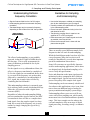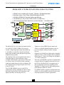
1
Critical Techniques for High-Speed A/D Converters in Real-Time Systems Critical Techniques for High Speed A/D Converters in Real-Time Systems First Edition Technology Theory Products Applications by Rodger H. Hosking Vice-President & Cofounder of Pentek, Inc. Pentek, Inc. One Park Way, Upper Saddle River, New Jersey 07458 Tel: (201) 818-5900 Fax: (201) 818-5904 Email: [email protected] Web Site: www.pentek.com Copyright ©2005 Pentek Inc. All rights reserved. Contents of this publication may not be reproduced in any form without written permission. Specifications are subject to change without notice. Pentek, GateFlow, ReadyFlow and VIM are a registered trademarks of Pentek, Inc. Other trademarks are owned by their respective companies. 1 Pentek, Inc. One Park Way, Upper Saddle River, NJ 07458 Tel: (201) 818-5900 Fax: (201) 818-5904 Email: [email protected] Web Site: www.pentek.com Critical Techniques for High-Speed A/D Converters in Real-Time Systems Section 1. A/D Markets and Technology Handbook Overview and Introduction High Speed A/D Converter Markets § A/D Technology and Markets § Commercial Wireless § Military Communications § Radar § Sonar § Telemetry § Beamforming § Direction Finding § Sampling and Filtering Techniques § New FPGA Technology for A/Ds § Serial Switched Fabrics for A/Ds § High Speed A/D Products § Applications § Summary Above are a list of topics covered in each section of this handbook, all related to the latest generation of high-speed A/D products for embedded real-time systems. § § § § § Wireless Networks Control Systems Signals Intelligence Medical Imaging Military Countermeasures § Nuclear Instrumentation § Structural Analysis Markets for high-speed A/D converters are significant in size and many are growing rapidly. New markets emerge regularly based on A/D technology advances, lower costs, and the general trend of replacing older mechanical and analog systems with digital signal processing (DSP) based systems. A/D (analog-to-digital) converters, frequently abbreviated as ADC, accept an analog voltage at the input and produce a digital representation of that voltage at the output called a sample. DSP offers significant advantages for handling signal complexity, communications security, improved accuracy and reliability, and reduced size, weight and power. Of necessity, many DSP systems require an A/D at the front. The two primary characteristics of A/Ds are the rate of conversion, or sampling rate, expressed in samples per second, and the accuracy of each digital sample expressed as the number of binary bits or decimal digits per sample. On the commercial side, high-speed A/Ds are used in wireless mobile communication systems, satellite systems, commercial radar systems for airliners, air traffic control towers and ships, as well as for wireless networks for home, office and public facilities. Sampling rates vary tremendously between applications. A digital medical thermometer may deliver samples to update the readout once every five seconds while a high speed wideband radar may produce 2 billion samples per second. Industrial uses include medical imaging systems and process control systems for manufacturing. The difference in sample rates between these two prominent examples is a staggering 10 orders of magnitude, and there are thousands of A/D applications spread continuously throughout this range. Government systems account for many of the high-end applications including phased array military radar, radar and communications countermeasure systems, global military radio networks, unmanned aerial vehicles and intelligence gathering systems. To help define the meaning of high speed A/D used in this handbook, we will be focusing primarily on A/D converters with sampling rates of 50 MHz and higher. 2 Pentek, Inc. One Park Way, Upper Saddle River, NJ 07458 Tel: (201) 818-5900 Fax: (201) 818-5904 Email: [email protected] Web Site: www.pentek.com Critical Techniques for High-Speed A/D Converters in Real-Time Systems 1. A/D Markets and Technology New Monolithic A/D Technology Monolithic A/D Converters for Fs ≥ 200 MHz and bits ≥ 8 § Smaller geometry, lower core voltages and power dissipation Manufacturer Part No. Sample Rate Chans No. Bits Input BW § Much higher sample rates and bit accuracy Atmel AT84AS008 2200 MHz 1 10 3300 MHz Atmel TS83102G0B 2000 MHz 1 10 3000 MHz Maxim MAX108 1500 MHz 1 8 2200 MHz § Wideband input circuitry optimized for direct IF sampling IF (intermediate frequency) signals are usually greater than Fs Differential, transformer coupled inputs minimize noise § High Performance Integrated S&H (sample-and-hold) Higher immunity to clock waveform symmetry and level § Improved multi-stage flash conversion techniques § Digital sample code generation and error correction Devices can be calibrated and trimmed during production § Improved thermal tracking of DC offset, gain, and linearity § Improved power supply noise rejection and immunity National ADC081000 1000 MHz 1 8 1700 MHz National ADC08D1000 1000 MHz 2 8 1700 MHz Atmel JTS8388B 1000 MHz 1 8 2000 MHz Maxim MAX104 1000 MHz 1 8 2200 MHz Atmel AT84AD001B 1000 MHz 2 8 1500 MHz Maxim MAX106 600 MHz 1 8 2200 MHz Atmel AT84AD004B 500 MHz 2 8 1000 MHz Maxim MAX101A 500 MHz 1 8 1200 MHz Atmel TS8308500 500 MHz 1 8 1300 MHz Maxim MAX1121 250 MHz 1 8 600 MHz AD9480 250 MHz 1 8 400 MHz TelASIC TS1410 240 MHz 1 14 500 MHz Analog Dev AD9430 215 MHz 1 12 700 MHz Analog Dev AD9410 210 MHz 1 10 500 MHz Analog Dev AD9054 200 MHz 1 8 350 MHz Analog Dev Because of all of these market segments, wideband A/D converters have made some tremendous advances in the last five years. Heres a long list of some of the commercially available, monolithic A/D converters with sampling rates of at least 200 MHz and resolution of at least 8 bits. This is partly due to silicon process improvements, but thats not all. Because many applications require direct sampling of IF signals well above 100 MHz, new wideband input stages were developed. These are all candidates for board level products for embedded systems. One of the most important advances is the sample-and-hold (or track-and-hold) at the front end. Notice Ive listed the input bandwidth at the right, just to highlight the importance of direct IF sampling applications, also call undersampling. Just as important, are new sample clock interfaces and drivers. In the next section, well discuss more about the principles and rules of sampling. At these speeds, you need state-of-the-art flash and multi-stage flash conversion techniques. New techniques in digital error code correction and thermal compensation circuitry help eliminate errors in bit accuracy, linearity and gain. Lastly, these new devices are more immune to power supply and system noise. 3 Pentek, Inc. One Park Way, Upper Saddle River, NJ 07458 Tel: (201) 818-5900 Fax: (201) 818-5904 Email: [email protected] Web Site: www.pentek.com Critical Techniques for High-Speed A/D Converters in Real-Time Systems Section 2. Sampling and Filtering Techniques Direct Baseband RF Signal Acquisition Analog RF Frequency Translation § Analog Translation to Baseband § Antenna signals are usually in the microvolt range § RF amplifier boosts signal to full scale input voltage of the A/D - usually 0 to +10 dBm § RF amplifier often includes a tuned bandpass filter centered on the signal of interest § No analog frequency translation before the A/D § Appropriate for HF signal frequencies (3 - 30 MHz) RF BANDPASS AMPLIFIER BASEBAND A/D CONVERTER § Analog Translation to IF (Intermediate Frequency) ANTENNA FILTER LOW PASS FILTER LOCAL OSCILLATOR RF BANDPASS AMPLIFIER RF AMPLIFIER MIXER A/D CONVERTER MIXER BANDPASS FILTER LOCAL OSCILLATOR IF A/D CONVERTER Intermediate Frequency Most receiver systems start with a signal originating from an antenna, and that signal is often at the microvolt level, so it must first be amplified by an RF amplifier stage. In case the antenna signal frequency is too high to be digitized directly by the A/D converter, it has to be translated down using an analog mixer and local oscillator. The amplifier is usually a tuned RF circuit which only passes the frequency band of interest, providing signal gain within that band and rejecting noise and unwanted signals in adjacent frequency bands. The top diagram shows a simplified representation of this analog translation to baseband with a low pass filter following the mixer. The bottom diagram shows the translation to an intermediate frequency or IF this is quite common. In this case, the filter is a bandpass filter centered at the IF frequency. If the RF input signal is at a low enough frequency, it can be digitized directly by an A/D converter, and no analog translation is necessary. So far, weve discussed three types of front end circuitry: For example, you can usually perform direct baseband sampling on HF signals with no translation required, since the frequency content is below 30 MHz. 1) Direct sampling with no translation (on the previous slide) 2) Analog translation to baseband 3) Analog translation to IF But how do we design the filters in each case? Lets go back to review some fundamental sampling theory. 4 Pentek, Inc. One Park Way, Upper Saddle River, NJ 07458 Tel: (201) 818-5900 Fax: (201) 818-5904 Email: [email protected] Web Site: www.pentek.com Critical Techniques for High-Speed A/D Converters in Real-Time Systems 2. Sampling and Filtering Techniques Filtering Helps Avoid Noise and Aliasing Fan Fold Paper Model to Visualize Sampling § Plot the spectrum of the input signal on transparent fan-fold printer paper scaled so the frequency axis is aligned with multiples of Fs on the backward folds § In all systems, the A/D input must be filtered for two important reasons: Eliminate out of band noise Eliminate aliasing Spectrum of RF Input Signal § Nyquist sampling theorem requires the input signal bandwidth must be less than one-half the sampling rate of the A/D converter § Some systems (like an IF stage) provide inherent bandlimiting before the A/D § Fundamental Sampling Modes 0 Fs/2 Fs 3Fs/2 2Fs 5Fs/2 3Fs Baseband Wideband Sampling Baseband Pre-select Sampling Undersampling Fan-fold Printer Paper Filters ahead of the A/D are needed primarily for two reasons: to eliminate out of band noise and to eliminate out of band signals that can cause aliasing. This simple technique has been very useful to our customers and our own applications engineers to help them understand what happens during sampling. Nyquist tells us that whenever sample a signal with an A/D, the bandwidth of that signal must be less than half the sampling rate of the A/D. Imagine that we have a stack of fan-fold computer printer paper with transparent sheets. Now, we assign the frequency axis along the bottom edge of this paper, scaled so that multiples of the sampling rate line up with the backward folds of the paper, as shown. Filters help us guarantee that this rule is met. Sometimes the bandwidth is already limited by the signal source, like the output of an IF stage that takes advantage of the IF filter bandwidth. But each case has to be analyzed individually. Now, using that frequency scale, we plot out the spectrum of the signal we want to sample, with amplitude plotted on the vertical axis. The design of the filter is also critically linked to the sampling mode. Here weve listed three fundamental sampling modes: 1) Baseband wideband sampling 2) Baseband pre-select sampling 3) Undersampling, which is also sometimes called sub-sampling To help you get a feel for the filter requirements of each mode, we present a convenient tool for analyzing the effects of sampling in the frequency domain. 5 Pentek, Inc. One Park Way, Upper Saddle River, NJ 07458 Tel: (201) 818-5900 Fax: (201) 818-5904 Email: [email protected] Web Site: www.pentek.com Critical Techniques for High-Speed A/D Converters in Real-Time Systems 2. Sampling and Filtering Techniques Fan Fold Paper Model to Visualize Sampling Baseband Sampling of Wideband Signals § For baseband signals over a wide frequency range, use a low pass filter with cutoff frequency, Fc, less than Fs/2, where Fs is the A/D sample rate § After sampling, only the baseband signal is captured, eliminating folding of aliased signals and noise § Now collapse the stack of transparent fan-fold paper and look through all the sheets § This represents how sampling folds the entire RF input spectrum into a single page from 0 to Fs/2 § Once aliasing occurs, there is no way to undo it 0 Fs/2 Signals of Low Pass Filter Interest Rejected Out-of-Band Signals and Noise Out of band signals and noise are all folded into the band between 0 and Fs/2 Fc Fs 0 Fs/2 Now lets collapse the stack of transparent paper flat together and hold the stack up to a light so we can see through all the sheets. 2Fs 3Fs/2 For the baseband wideband sampling mode, where we want to look at everything from DC up to a frequency below the half sampling rate, we can install a low pass filter with a cutoff frequency, Fc, located below Fs/2. We are now looking at the frequency plot of the sampled signal at the output of the A/D converter. Notice that weve lost a lot of information because we cant tell which sheet a particular signal is on. And, unfortunately, after sampling, that information is lost forever. The frequency response of the filter is shown in green. Now all of the out-of-band signals and noise on the pages above Fs/2 are eliminated so that when the folding occurs, it doesnt corrupt the baseband signal. Weve also contaminated any particular signal with signals from other sheets which have folded on top of it. Not only that, weve also folded the noise from all the sheets so they pile up in the region between DC and the half sampling rate, potentially ruining your signal to noise ratio. How do we avoid this mess in each of the three sampling modes? 6 Pentek, Inc. One Park Way, Upper Saddle River, NJ 07458 Tel: (201) 818-5900 Fax: (201) 818-5904 Email: [email protected] Web Site: www.pentek.com Critical Techniques for High-Speed A/D Converters in Real-Time Systems 2. Sampling and Filtering Techniques Baseband Sampling of Pre-Select Signals Principles of Undersampling § For narrowband signals above Fs/2, undersampling can be used to intentionally alias the input signal § Very useful for IF outputs of UHF/VHF receivers § Successful undersampling needs careful selection of: § For narrowband signals at baseband, using a preselect bandpass filter can optimize the dynamic range of the A/D converter by rejecting strong adjacent signals and out-of-band signals and noise § Pre-select filter is a bandpass filter whose passband is centered on the signal of interest Unwanted Adjacent Signal of Pre-Select Signal Filter Interest Signal Frequency Signal Bandwidth Bandpass Filter Sampling Frequency Signal of Interest Rejected Out-of-Band Signals and Noise 0 0 Fs Fs/2 2Fs Fs Fs/2 2Fs 3Fs/2 3Fs/2 The third sampling mode, called undersampling or sub-sampling, is ideal for many systems that use an analog RF translator front end. These receivers usually deliver IF outputs, often at 21.4 or 70 MHz, with bandwidths ranging from a few kilohertz to tens of MHz, depending on the receiver. For the baseband pre-select sampling mode, we need to use a bandpass filter with the frequency response shown in green. We get the same benefits as the previous case for out-of-band signals and noise above Fs/2, but more importantly, we can keep large adjacent signals like the one shown, from getting to the A/D converter. If we wanted to perform baseband sampling on a 70 MHz signal, we would have to choose a sampling rate of well over 140 MHz. This may require an A/D that adds cost and power to the system. The reason for this is that if the large unwanted signal gets through to the A/D converter, it uses up the dynamic range of the A/D. However, because the IF signal is inherently bandlimited, we can take advantage of the folding caused by sampling and use a lower frequency A/D. For applications where there are known, strong unwanted signals, this technique can be extremely useful in improving the signal-to-noise ratio of the smaller signal of interest. This is a little tricky since you have to carefully choose the sampling frequency and filtering according to the signal frequency and bandwidth. Lets see how. 7 Pentek, Inc. One Park Way, Upper Saddle River, NJ 07458 Tel: (201) 818-5900 Fax: (201) 818-5904 Email: [email protected] Web Site: www.pentek.com Critical Techniques for High-Speed A/D Converters in Real-Time Systems 2. Sampling and Filtering Techniques Principles of Undersampling Design: Step 1 Principles of Undersampling Design: Step 2 § Step 2: Choose a sampling frequency so that the filter pass band and skirts fall entirely within one page of the fan-fold paper § Tradeoffs § Step 1: Design a bandpass filter or IF filter to pass the band of interest and reject all other signals to meet spurious and S/N requirements § Tradeoffs Higher sampling rate allows broader bandwidth & simpler filter Sharper filter adds complexity, expense, calibration, space, etc. Sharper filter allows lower A/D sample rate Unwanted Out-of-Band Signals 0 Band Pass or IF Filter Signal of Interest Fs Fs/2 A/Ds with lower sampling rates are more accurate & less expensive Unwanted Out-of-Band Signals Fs/2 3Fs/2 Signal of Interest Fs 0 2Fs Band Pass or IF Filter 3Fs/2 The fan fold paper really comes in handy here. Here are some trade-offs to consider. First, design a bandpass filter that rejects unwanted signals and noise. With a higher sampling rate, the pages are wider and the filter becomes less complex. Also, there is a lower noise density folded into the 0 to Fs/2 band after sampling. This is often fully satisfied by the standard IF filter in the RF translator, but you do have to check this. At higher sampling rates, however, the A/D is more expensive and the number of bits of accuracy drops off. Sharper filters add cost and maintenance but they do let you get away with a lower sampling rate as well see on the next slide. You also need to be sure that the A/D has a good wideband input stage to handle the IF signal with minimum distortion. Second (top of next column), choose a sampling frequency so that the passband of the filter, along with its skirts, falls entirely on a single page of fan fold paper. Equally important is the aperture uncertainty or phase jitter of the sample-and-hold amplifier, which is usually part of the A/D. There are many possible solutions to each case, so you have to pick the one that works best. You may have to go back and forth a few times to readjust the filter and sampling rate to get the best scheme. To make this job easier, many A/D converters are now specifically characterized to operate in undersampling applications. 8 Pentek, Inc. One Park Way, Upper Saddle River, NJ 07458 Tel: (201) 818-5900 Fax: (201) 818-5904 Email: [email protected] Web Site: www.pentek.com Critical Techniques for High-Speed A/D Converters in Real-Time Systems 2. Sampling and Filtering Techniques Undersampling Performs Frequency Translation Guidelines for Sampling and Undersampling § Use the fan fold paper to validate your sampling plan for the characteristics your input signal § Carefully evaluate A/D specifications for operation in the undersampling mode § Ensure low-noise, wideband circuitry in the front end ahead of the A/D § Transforming coupling often is superior to an amplifier for IF or RF input signals § Eliminate as many out of band signals and noise as possible, since they will fold § Ensure the the sample clock is clean with low phase noise and jitter § Signal of interest folds into the 0 to Fs/2 region § Undersampling performs an automatic frequency translation § Translated image may be reversed in frequency depending on which side of the fold the input falls Signal of Interest Folded to Baseband 0 rsed Rev e No rm al rsed Rev e Fs/2 There are usually several different sample clock frequencies that will work for undersampling. While the fanfold paper model can show all of the correct frequency plans, the best choice will usually be determined by several other important practical considerations shown above. The effect of undersampling, as you probably expected, is that the IF signal is folded down to the first page. This is really an automatic frequency translation, performed for free by the sampling process. Some A/D converters are specifically characterized for undersampling applications, while others are designed only for baseband sampling, so be sure to verify the specifications. For the signals on every odd numbered sheet, the effect is a frequency translation by a multiple of Fs. For the signals on even numbered sheets, there is a reversal of the frequency axis on that sheet, followed by a translation by an odd multiple of Fs/2. Again, this is much easier to follow by visualizing the fan-fold model. Noise and distortion on the input signal must be minimized so these components dont fold into the sampled signal. Special care must be taken preserve the purity of the sample clock signal. Undersampling can be an extremely valuable tool for software radio applications, since it can eliminate at least one additional stage of analog frequency translation and simplify system design. This undersampling technique is extremely popular in software radio systems which almost always follow the A/D converter with a digital down converter (DDC). Undersampling allows you to use an A/D converter with a lower sampling rate, which usually means more bits of resolution and better dynamic range. This lower sample rate also reduces the cost and complexity of the next stage of digital signal processing, recording, storage, or transmission. Regardless of where the undersampling folding process translated the signal of interest, the DDC can translate it down to 0 Hz as a complex baseband signal. Once the complex signal is at baseband, the reversal of the frequency axis is easily undone by simply changing the sign of the Q component. 9 Pentek, Inc. One Park Way, Upper Saddle River, NJ 07458 Tel: (201) 818-5900 Fax: (201) 818-5904 Email: [email protected] Web Site: www.pentek.com Critical Techniques for High-Speed A/D Converters in Real-Time Systems Section 3. FPGA Technology FPGAs: The Essential Companion for High Speed A/Ds § § § § § § § § § § § § FPGAs: New Development Tools On-chip processor cores Internal clock rates up to 600 MHz Reduced power with core voltages near 1 volt Dedicated on-chip hardware multipliers Memory densities of over 10 million bits High-density BGA and flip-chip packaging Flexible memory structures Logic densities of over 10M gates Silicon geometries near 0.1 microns On-board giga-bit serial interfaces Over 1200 user I/O pins Configurable interface standards § High Level Design Tools Block Diagram System Generators Schematic Processors High-level language compilers for VHDL & Verilog Advanced simulation tools for modeling speed, propagation delays, skew and board layout Faster compilers and simulators save time Graphically-oriented debugging tools § IP (Intellectual Property) Cores FPGA vendors offer both free and licensed cores FPGA vendors promote third party core vendors Wide range of IP cores available FPGAs, or Field Programmable Gate Arrays, are commonly coupled to high speed A/Ds for several key reasons: they can perform real-time digital signal processing faster than general purpose programmable processors and they offer extremely high speed interfaces to other system components, including built-in interfaces to the new high-speed serial switched fabrics. To support such powerful devices, a whole new world of design tools are appearing that now open up FPGAs to both hardware and software engineers. Instead of just accepting logic equations and schematics, these new tools accept entire block diagrams as well as VHDL and Verilog definitions. Choosing the best FPGA vendor often hinges heavily on the quality of the design tools available to support the parts. BGA and flip chip packages provide plenty of I/O pins to support these on-board gigabit serial transceivers and other user-configurable system interfaces. To minimize some of the tricky timing work for hardware engineers, excellent simulation and modeling tools help you quickly analyze worst case propagation delays and suggest alternate routing strategies to minimize them within the part. This can really save you hours of tedious trouble shooting, not only during design verification but also for production testing. Other important features are on-chip processor cores, computation clocks of up to 600 MHz, and lower core voltages to keep power and heat down. In the late 1990s, dedicated hardware multipliers started appearing and now youll find literally hundreds of them on chip as part of the DSP initiative launched by virtually all FPGA vendors. In the last few years, a new industry of third party IP or intellectual property core vendors now offer thousands of application-specific algorithms, ready to drop into the FPGA design process to help beat the time-to-market crunch and to minimize risk. High memory densities coupled with very flexible memory structures meet a wide range of data flow strategies. Logic slices with the equivalent of over 10 million gates result from silicon geometries shrinking down to 0.1 microns. 10 Pentek, Inc. One Park Way, Upper Saddle River, NJ 07458 Tel: (201) 818-5900 Fax: (201) 818-5904 Email: [email protected] Web Site: www.pentek.com Critical Techniques for High-Speed A/D Converters in Real-Time Systems 3. FPGA Technology FPGAs: Key Resources for DSP FPGAs Bridge the Software Radio Application Task Space § Parallel Processing § Hardware Multipliers for DSP A/D CONVERSION FPGAs can now have over 500 hardware multipliers Process Intensity § Flexible Memory Structures Dual port RAM, FIFOs, shift registers, look up tables, etc. § Parallel and Pipelined Data Flow Systolic simultaneous data movement § Flexible I/O Supports a variety of devices, buses and interface standards § High Speed § Available IP cores optimized for special functions FPGAs DIGITAL RECEIVER FILTER ASICs DEMOD DECODE DSPs FFT ANALYSIS DECISIONS Flexibility Like ASICs, all of the logic elements in FPGAs can execute in parallel. This includes the hardware multipliers, and you can now get over 500 of them on a single FPGA. As a result, FPGAs have significantly invaded the application task space as shown by the center bubble in the task diagram above. They offer the advantages of parallel hardware to handle some of the high process intensity functions like digital receivers, and the benefit of programmability to accommodate some of the decoding and analysis functions of DSPs. This is in sharp contrast to a programmable DSP, which normally have just a handful of multipliers that must be operated sequentially, instead. FPGA memory can now be configured in the design tool to implement just the right structure for your task including dual port RAM, FIFOs, shift registers and other popular memory types. These advantages may come at the expense of increased power dissipation and increased product costs, but these considerations are often secondary to the performance and capabilities of these remarkable devices. These memories can be distributed along the signal path, interspersed with the multipliers and math blocks, so that the whole signal processing task operates in parallel, in a systolic pipelined fashion. Again, this is dramatically different from sequential execution and data fetches from external memory in a programmable DSP. As weve said, FPGAs now have specialized serial and parallel interfaces to match requirements for high speed peripherals and buses. 11 Pentek, Inc. One Park Way, Upper Saddle River, NJ 07458 Tel: (201) 818-5900 Fax: (201) 818-5904 Email: [email protected] Web Site: www.pentek.com Critical Techniques for High-Speed A/D Converters in Real-Time Systems 3. FPGA Technology Evolving FPGA Generations § § § § Xilinx FPGAs in Pentek Products Virtex-II: 18x18 hardware multipliers for DSP Virtex-II Pro: Dual PowerPC microcontrollers Virtex-II Pro: Gigabit serial transceivers for switched fabric Virtex-4: Lower Power, Higher Density, Gig ENET Pentek Hardware Available FPGA Resources Xilinx Virtex-E Virtex-II Virtex-II Pro Virtex-4SX Virtex-4 FX XCV600E XC2V3000 XC2VP50 XCE4VSX55 XCE4VFX100 Xilinx Virtex II Pro XC2V1000 XC2V3000 XC2VP20 XC2VP50 CLB Array (row x column) 48 x 72 40 x 32 64 x 56 56 x 46 88 x 70 Logic Cells 15,552 11,520 32,256 20,880 53,136 986k 1000k 3000k 2600k 6000k n/a 5,120 14,336 9,280 23,616 295k 720k 1728k 1584k 4176k - 40 96 88 232 System Gates CLB Slices Virtex-E Xilinx Virtex II XCV600E Max Block Ram (bits) 18 x 18 Multipliers Pentek Model Board Type No. of FPGAs % Available to User % Available to User % Available to User 15,552 32,256 53,136 55,296 94,896 Gates RAM Max Block RAM (bits) 295k 1,728k 4,176k 5,760k 6,768k 4205 VME 2 - - 86%* 90%* 95%* 96%* - - - - Max I/O User Pins 512 720 852 640 768 6228 VIM-2 2 - - 82% 100% - - - - 18x18 Multipliers - 96 232 512 160 6230 VIM-4 2 70% 100% - - - - - - - - - 2 - 2 VIM-2 1 70% 100% - - - - - - - - 405 PowerPC Cores - 6231 6232 VIM-4 2 70% 100% - - - - - - - - RocketIO Serial - - 16 - 20 6235 VIM-2 1 - - 82% 100% 94% 100% - - - - Gbit ENET Ports - - - - 4 6236 VIM-2 1 - - 82% 100% 94% 100% - - - - 6250 VIM-2 2 - - 92% 100% 97% 100% - - - - 6251 VIM-2 2 - - - - - - 98% 100% 99% 100% 6256 VIM-2 2 - - - - - - 98% 100% 99% 100% 6821 VME 2 - - - - - - 98% 100% 99% 100% 6822 VME 2 - - - - - - 98% 100% 99% 100% 7131 PMC 1 - - 15% 5% 70% 60% - - - - 7140 PMC 1 - - - - - - TBD TBD TBD TBD 7231 cPCI 2 - - 15% 5% 70% 60% - - - - 7331 cPCI 1 - - 15% 5% 70% 60% - - - - 7631 PCI 1 - - 15% 5% 70% 60% - - - - Logic Cells This table shows three four of Xilinx devices used in current and future Pentek Products: the Virtex-E, the Virtex-II, the Virtex-II Pro and the Virtex-4.. The Virtex-E family includes a generous mix of configurable logic blocks, logic cells, system gates and block memory. Slices RAM Slices RAM Slices RAM 94% 100% Slices RAM The chart above shows these three families of FPGAs with the various Pentek hardware products that use them. The Virtex-II family added built in hardware multipliers a major benefit for software radio signal processing that supports digital filters, averagers, demodulators and FFTs. Each hardware product uses some of the FPGA resources to implement some of the standard factory functions of the products, such as interfaces, data formatting, state machines, and operating modes. The Virtex-II Pro family dramatically increased the number of hardware multipliers and also added embedded PowerPC microcontrollers. The Virtex-II Pro is also the first family to incorporate Rocket I/O multi-gigabit serial transceivers to support the new switched serial fabrics. However, since many of the newer FPGAs are so large, even after all of the standard factory functions have been implemented, a significant percentage of FPGA resources remain unused and available for customer use. The three part Virtex-4 family -- namely LX, FX, and SX --offers various combinations of significantly higher resources densities with reduced power dissipation. For the first time, built in gigabit ethernet interfaces offer power connections to external system devices. This chart shows the percentage of unused system gates and RAM available to the user for extending the FPGA to include custom algorithms. Pentek has developed the GateFlow FPGA Design Resources to address this requirement. 12 Pentek, Inc. One Park Way, Upper Saddle River, NJ 07458 Tel: (201) 818-5900 Fax: (201) 818-5904 Email: [email protected] Web Site: www.pentek.com Critical Techniques for High-Speed A/D Converters in Real-Time Systems 3. FPGA Technology Penteks GateFlow FPGA Design Resources GateFlow FPGA Design Kit GateFlow IP Core Library GateFlow FPGA Design Kit § Allows FPGA design engineers to easily add functions to standard factory configuration GateFlow Factory Installed IP Cores § Includes VHDL source code for all standard functions: Control and status registers A/D and Digital receiver interfaces Mezzanine interfaces Triggering, clocking, sync and gating functions Data packing and formatting Channel selection A/D / Receiver multiplexing Interrupt generation Data tagging and channel ID § User Block for inserting custom code Penteks GateFlow Design Resources offers three ways to take advantage of these FPGA products. If you want to add your own algorithms to Pentek catalog products, we offer the GateFlow FPGA Design Kit that includes VHDL source code for all of the standard factory functions. If you want to add your own custom algorithms, we offer the GateFlow FPGA Design Kit. If you need off the shelf algorithms for highperformance software radio functions you can take advantage of the GateFlow IP (Intellectual Property) Core Library. VHDL is one of the most popular languages used in the FPGA design tools. The GateFlow Design Kit includes the VHDL source code for every software module we used to create these standard factory features of the product. The third strategy is our GateFlow Factory Installed Cores available as product options for many FPGA-based software radio products. The standard factory configuration supports a wide range of operating modes, timing and sync functions, as well as several different data formatting options. Lets start with the GateFlow FPGA Design Kit. This includes control and status registers, peripheral interfaces, mezzanine interfaces, timing functions, data formatting, channel selection, interrupt support data tagging. These are all fully supported with our ReadyFlow libraries and device drivers. We also include a special User Block positioned right in the data stream so you can easily drop in your own custom signal processing algorithm. 13 Pentek, Inc. One Park Way, Upper Saddle River, NJ 07458 Tel: (201) 818-5900 Fax: (201) 818-5904 Email: [email protected] Web Site: www.pentek.com Critical Techniques for High-Speed A/D Converters in Real-Time Systems 3. FPGA Technology GateFlow Design Kit User Block GateFlow Design Kit Project Files § Simplified view of typical VHDL source code modules § User Block pins defined for input, output, control, status, & clocks § Data path is factory configured as a straight wire DIGITAL INPUT ANALOG INPUT FPGA USER BLOCK A/D DATA SELECT DIGITAL RECEIVER EXT CLK LVDS CLK & SYNC XTAL OSC CLOCK & SYNC DRIVERS INPUT OUTPUT DEFAULT BYPASS § Project files for Xilinx Foundation ISE Tools Archived project files for default factory configuration for standard factory product operation VHDL source code for all project files MEZZANINE INTERFACE Software module interconnect block diagram DATA FORMATTER JTAG chain definition files User Block I/O connections diagram CONTROL STATUS DMA CONTROL & COUNTERS CLOCK CONTROL STATUS & CONTROL § Other files INTERRUPT GENERATOR Pentek FPGA Design Kit Users Manual FPGA manufacturers data sheet and users guide SYNC / GATE / TRIGGER GENERATOR § FPGA Loader Utility Heres a simplified block diagram of a typical software radio module showing the FPGA as the large green box and external hardware devices connected to it. The GateFlow Design Kit is intended to be used with the Xilinx ISE Foundation Tool Suite and customers should be trained and familiar with this tool and FPGA design principles, in general. The yellow blocks inside the FPGA are VHDL code modules that handle the standard factory functions and interfaces. The design kit installs as a complete project file within the ISE environment and includes all of the project files that Pentek engineers used to create the standard factory product. These include configuration and definition files, VHDL source, JTAG definition files and I/O block diagrams. The User Block is a VHDL module that sits in the data path with pin definitions for input, output, status, control and clocks. In the standard product, the User Block is configured as a straight wire between input and output. The design kit also includes several utilities, but one important resource is the FPGA Loader Utility. If the FPGA designer can create an IP core or a custom algorithm inside the User Block so that it conforms to the pin definition, he will have a very low risk experience in re-compiling and installing his custom code. And remember, he can also make changes outside of the User Block, since we provide source code for all the modules. 14 Pentek, Inc. One Park Way, Upper Saddle River, NJ 07458 Tel: (201) 818-5900 Fax: (201) 818-5904 Email: [email protected] Web Site: www.pentek.com Critical Techniques for High-Speed A/D Converters in Real-Time Systems 3. FPGA Technology GateFlow Design Kit FPGA Loader Utility Supports easy FPGA reconfiguration for field upgrades Eliminates need to disassemble system to modify hardware Extends product longevity § Tested and Certified for Pentek Products Receivers, A/D, D/A, FPDP, FPGAs, Digital I/O, etc § Suitable for any Xilinx FPGA Platform (not just Pentek) § Compatible with GateFlow FPGA Design Kit FPGA § Licensing based on Xilinx SignOnce Project License DATA STREAM Supports easy FPGA reconfiguration during runtime for adaptive processing § Pentek is a Xilinx AllianceCore Member High Performance I/O CONTROL FPGA configuration loader utility executes on host or baseboard processor Front Panel I/O CONF IGURA TION § FPGA Loader Utility GateFlow IP Core Library Customers use a common, pre-approved standardized license Streamlines legal process and simplifies ordering Core may be incorporated into any single project or product No limit on the number of licensed products produced Bi-FIFO Processor Node Pentek is an AllianceCore Member, a third party program sponsored by Xilinx for companies that specialize in specific areas of expertise in developing FPGA algorithms for niche application areas. These include image processing, communications, telecom, telemetry, signal intelligence, wireless communications, wireless networking and many other disciplines. Global I/O GLOBAL RESOURCES Backplane I/O SYSTEM BACKPLANE Normally, the FPGA is loaded from a nonvolatile EEPROM with the standard factory configuration code when the product is powered up. The FPGA Loader Utility allows the processor associated with the FPGA product to reconfigure the FPGA as a software task, effectively overwriting the factory configuration code. Pentek offers several very high performance GateFlow IP Cores for DSP which can be used on Pentek products and other Xilinx platforms. They are fully compatible with the GateFlow FPGA Design Kit we just discussed. This can be done without turning off power, without disassembling the board or system, and without attaching any special cables or harnesses to the board. The cores are sold under the standardized Xilinx SignOnce Project License which allows customers to pay once for unlimited use of the core within a given project. In this way, the FPGA can be reconfigured during initialization to install custom operational modes and features. It can also facilitate product upgrades and enhancements to dramatically extend product longevity. The Loader Utility is especially useful as a runtime resource so that during operation, a user of the product can select a new mode of operation, and cause a new FPGA configuration upload to implement that mode as part of the runtime executable code. 15 Pentek, Inc. One Park Way, Upper Saddle River, NJ 07458 Tel: (201) 818-5900 Fax: (201) 818-5904 Email: [email protected] Web Site: www.pentek.com Critical Techniques for High-Speed A/D Converters in Real-Time Systems 3. FPGA Technology GateFlow IP Cores for Software Radio Core 401 403 404 421 422 440 Quad Pipelined FFT Cores Description 1k-point Quad Radix-4 Complex FFT 4k-point Single Radix 4 Complex FFT 4k-point Quad Radix-4 Complex FFT 160 MHz Wideband Digital Down Converter 296 MHz Wideband Digital Down Converter Pulse Compression Radar more to come !! § FFT Calculation Time Depends on FPGA Clock § FPGA Clock = Data Source Sample Clock § Maximum FPGA clock rates depend on Xilinx speed grade Xilinx FPGA Speed Grade Max Clock Core 401 Quad 1k FFT Quad Core 404 Quad 4k FFT Quad Core 403 Single 4k FFT Single -7 160 MHz 1.60 usec 6.40 usec 25.60 usec -6 140 MHz 1.83 usec 7.31 usec 29.25 usec -5 127 MHz 2.01 usec 8.06 usec 32.25 usec -4 111 MHz 2.31 usec 9.23 usec 36.90 usec (reference) 100 MHz 2.56 usec 10.24 usec 40.96 usec § Comparison: 4k FFTs on Programmable Processors 500 MHz G4 AltiVec PowerPC: 105 usec (VSIPL Library) > 10X 300 MHz TMS320C6203 DSP: 212 usec (TI Benchmarks) > 20X This is the list of GateFlow IP Cores available from Pentek. The first three are FFTs, followed by two wideband digital down converters, and a radar pulse compression core. Dozens of FFT IP cores are available but here are three examples of 1k and 4k complex FFTs that have been optimized for speed. Lets start with the FFT cores. Calculation time is proportional to clock speed and the maximum clock depends on the speed grade of the FPGA devices. For these cores, the -7 device can be operated up to 160 MHz. But at a reference clock frequency of 100 MHz, the core 404 executes a 4k complex FFT in just over 10 usec. So, how does that compare with a general purpose DSP or RISC processor? In fact, a 500 MHz G4 PowerPC takes ten times longer and a 300 MHz TI C6203 takes 20 times longer. The message here is that if need to do an FFT, strongly consider doing it in an FPGA. 16 Pentek, Inc. One Park Way, Upper Saddle River, NJ 07458 Tel: (201) 818-5900 Fax: (201) 818-5904 Email: [email protected] Web Site: www.pentek.com Critical Techniques for High-Speed A/D Converters in Real-Time Systems 3. FPGA Technology Pipelined FFT Data Flow IP Cores 401 and 404 Wideband Digital Downconverter IP Core 421 § Cores 401 & 404 use QUAD pipelined architecture § § § § § Four input & output streams staggered at 25% offset Four input/output points for each input clock § FFT calculation time for Core 404 (4096 points) Operates at input clock rates to 160 MHz Real or complex output, spectrum inversion & offset Requires XC2V1500 Xilinx Virtex-II FPGA (or larger) Two will fit inside the XC2V3000 Four FFTs are computed in parallel every 4096 clocks Effective Calculation for each FFT = 4096 clocks / 4 = 1024 clocks 100 MHz Clock Example: 4k FFT Time = 1024 x 10 ns = 10.24 usec Mixer Complex Input 1024 input samples 4096 4096 input samples 4096 input samples 4096 input samples Core 404 Quad Parallel Pipelined 4k FFT engine 25% input offset I Q 16 Complex Mixer 16 Filter I Q I FIR Lowpass Complex Filter Q 4096 FFT points 4096 FFT points Sin/Cos LUT 4096 FFT points Local Oscillator 4096 FFT points Phase Accum Tuning Frequency 25% output offset Coefficient LUT Decimator & Formatter I Q Real Baseband Digital Outputs Decimation Factor & Output Mode Filter Coefficients CLOCK This wideband digital down converter is classic architecture of mixer, local oscillator and filter that takes full advantage of the hardware multipliers and memory inside the Virtex-II devices. Heres a simplified view of the data flow into, and out of, the four stage FFT engine for the 4k point FFT. Four separate input streams are processed in parallel with a 25% offset between the streams. It offers real or complex outputs and outputs in several formats, six decimation settings from 2 to 64 and four sets of user loadable FIR coefficients for each setting. This explains why the effective FFT calculation time for engine is 25% of the data collection time. This core supports one channel with 75% input overlap processing, two channels with 50% input overlap processing or four independent channels with no overlap. It operates at a maximum frequency of 160 MHz. Unfortunately, it wont work for A/D converters operating at higher frequencies, like the AD9430 12-bit 215 MHz A/D converter. So, how we solve that problem? 17 Pentek, Inc. One Park Way, Upper Saddle River, NJ 07458 Tel: (201) 818-5900 Fax: (201) 818-5904 Email: [email protected] Web Site: www.pentek.com Critical Techniques for High-Speed A/D Converters in Real-Time Systems 3. FPGA Technology Wideband Digital Downconverter IP Core 422 Wideband DDC Performance § Targets AD9430 215 MHz 12 -bit A/D Converter products GC1012B § Core operates at input clock rates to 296 MHz § Demultiplexer sends alternate samples into each stage § Each stage operates at one half the input clock rate § Formatter combines two stages into a single output § Requires XC2V3000 Xilinx Virtex -II FPGA (or larger) I 16 I I Q Q Complex Input Q 16 FIR Lowpass Filter Local Osc NCO I I Q Q FIR Lowpass Filter I Q Combiner & Decimator & Formatter I Q Baseband Digital Real Outputs Local Osc NCO By taking advantage of the ability to build parallel hardware structures in FPGAs, we can split the single input stream from the A/D into two simultaneous processing chains. Core 422 12 bits Real Only Maximum Input Data Rate 100 MHz 160 MHz 296 MHz 50MHz 28 bits None 12 bits 75 dB 13 bits One Fixed 14 bits ±0.1 dB 75 dB 10 to 16 bits 80 MHz 148 MHz Maximum Input Bandwidth NCO Frequency Resolution NCO Phase Offset NCO Output Resolution NCO (SFDR) Mixer Output Resolution Number of FIR Filter Sets FIR Filter Programmability FIR Coefficient Resolution Default 80% Filter Ripple Default 80% Image Rejection Output Resolution I Q Core 421 Input Resolution Input Format 16 bits Real or Complex 32 bits 32 bits 18 bits 110 dB 17 bits Four User Programmable 18 bits ±0.04 dB 100 dB 16 or 24 bits Compared with the industry standard ASIC equivalent, the 421 and 422 Cores deliver higher sample rates, programmable filter coefficients and much better overall signal to noise performance because of improved bit accuracies in each stage. At the front end of the Core 422 wideband receiver, a demultiplexer sends even samples to the upper DDC arm and odd samples to the lower DDC arm. In fact, four user selectable sets of FIR filter coefficients are available for each of the six decimation settings. These 24 sets of coefficients are stored in RAM structures within the FPGA so users can enter new coefficient values during runtime with no need for recompiling the FPGA. A final stage combines the two decimated DDC streams into a single output. In this way, a 296 MHz input sample stream can be handled with two 148 MHz DDC cores operating in parallel. What about performance of this core compared with an ASIC device? 18 Pentek, Inc. One Park Way, Upper Saddle River, NJ 07458 Tel: (201) 818-5900 Fax: (201) 818-5904 Email: [email protected] Web Site: www.pentek.com Critical Techniques for High-Speed A/D Converters in Real-Time Systems 3. FPGA Technology Dowloadable Evaluation IP Core Models Factory Installed IP Cores § Popular signal processing functions § Standard off-the-shelf hardware § Optimized for specific mezzanine cards § Optimized for efficient FPGA resource utilization § Optimized for execution & throughput speed § Eliminates need for FPGA development § Specified as an option to standard products § No licensing or NDA Required § Pentek ReadyFlow Board Support Libraries § Customers can download an evaluation copy § Download from Pentek GateFlow IP Core web page § Evaluation core can be tested under simulation § Requires Xilinx ModelSim FPGA simulation tool § Core can be tested for function, size, & accuracy All of these IP cores can be evaluated before purchasing simply by downloading an evaluation model from the Pentek web site at: www.pentek.com/gateflow This model file can be installed and run on the Xilinx ModelSim tools to check size, accuracy and function of all the IP core resources. The third GateFlow offering is the family of GateFlow Factory Installed IP Cores. Pentek will install selected IP cores from the GateFlow IP Core Library on Pentek catalog products. This is done by simply appending an option number to the model number. All installed cores are fully tested and supported with Pentek ReadyFlow Board Support Libraries. These installed cores allow customer to take advantage of these turbo charged products without investing in FPGA design skills and resources. 19 Pentek, Inc. One Park Way, Upper Saddle River, NJ 07458 Tel: (201) 818-5900 Fax: (201) 818-5904 Email: [email protected] Web Site: www.pentek.com Critical Techniques for High-Speed A/D Converters in Real-Time Systems 3. FPGA Technology Extended Wideband DDC Installed IP Core § § § § GateFlow Summary § GateFlow Design Kit Tunable across a 107.5 MHz range Output bandwidths from 2.5 MHz to 86 MHz Decimation settings: 2, 4, 8, 16, 32, & 64 User programmable filter coefficients 16 MB FLASH RF In 170 MHz 215 12-Bit A/D AD9430 Fs Ext Clk XTAL OSC Front Panel LVDS Timing Bus 128 MB SDRAM 16 MB FLASH CLOCK, SYNC & TRIGGER GENERATOR LOCAL OSCILLA TOR § GateFlow IP Core Library PENTEK 6821 215 MHz A/D VME Board COMPLE X DECIMA TING MIXE R FIR FILTE R Outstanding performance from optimized algorithms Validated designs proven on Pentek hardware Extensive documentation and test benches OUTP UT V XS or FPDP § GateFlow Factory Installed IP Cores Xilinx XC2VP50 With GateFlow Factory Installed 422 DDC Core LOCAL OSCILLA TOR Fs/2 Known good model serves as a reference starting point User block eliminates design effort for hardware I/O Cookbook instructions and flexible FPGA loader utilities Outstanding performance from optimized algorithms Eliminates FPGA design tasks with ready -to-use solution Thoroughly tested, documented, and supported with ReadyFlow 128 MB SDRAM COMPLE X DECIMA TING MIXE R FIR FILTE R OUTP UT V XS or FPDP Xilinx XC2VP50 With GateFlow Factory Installed 422 DDC Core In summary, GateFlow FPGA Design Resources offer three ways to extend the functions of FPGAs. The new 215 MHz A/D converter featured on the Pentek Model 6821 and 6822 VXS A/D Converter boards can accommodate two Core 422 Extended Wideband DDC IP Cores. The GateFlow FPGA Design Kit allows customers to add their own algorithms to Pentek catalog products. The two Xilinx XC2VP50 devices are configured as two independently controlled digital down converters with a tuning range from DC to 107.5 MHz and output bandwidths as high as 86 MHz. The GateFlow IP Core Libraries are highperformance DSP algorithms available for any Xilinx platform. The GateFlow Factory Installed Cores allow customers to add powerful FPGA resources to Pentek board level products easily and with full software library support. 20 Pentek, Inc. One Park Way, Upper Saddle River, NJ 07458 Tel: (201) 818-5900 Fax: (201) 818-5904 Email: [email protected] Web Site: www.pentek.com Critical Techniques for High-Speed A/D Converters in Real-Time Systems Section 4. Switched Serial Fabrics New Switched Serial Fabric Technology What is a Switched Fabric? § All data information is sent in well defined packets § A Switched Fabric is a system of connecting devices together with packet links using switches to allow multiple simultaneous data transfers § The fabric switch connects source and destination devices according to the packet routing information Header Data Pay load Checksu m Device § Packets usually include: Header information to identify source, destination, packet type, data size, time stamp, sequence number, and priority Crossbar Switch Device Device Device Device Device Data payload Footer information for checksum and end of packet marker § First switched fabrics used parallel data paths RACEway, SkyChannel, etc § Packet protocols differ between standards § New switched fabrics utilize gigabit (GHz) serial data links § Some protocols include various levels of error checking and error correcting A switched fabric system connects devices together to support multiple simultaneous data transfers, usually implemented with a cross bar switch. Weve seen how FPGAs now offer built-in serial gigabit interfaces to support the new serial switched fabrics. This section Well start with the basic principles and then look at some of exciting emerging standards. The packet header provides the necessary routing information between source and destination. The traffic in switched fabric consists of packets that contain a packet information header, the payload data itself, and then usually a footer at the end for integrity. Most of you already know about some existing parallel switched fabrics for backplanes such as RACEway and SkyChannel. The new generation of switched fabrics uses gigabit serial links instead, and there are many contenders for backplane traffic in embedded systems. Its like a package sent into the FedEx system the barcode on the label makes sure it gets through the system and to where its going on time. Lets look at the most popular ones. Each protocol uses different packet structures and some contain error checking and even error correction. Now lets see how the switching works. 21 Pentek, Inc. One Park Way, Upper Saddle River, NJ 07458 Tel: (201) 818-5900 Fax: (201) 818-5904 Email: [email protected] Web Site: www.pentek.com Critical Techniques for High-Speed A/D Converters in Real-Time Systems 4. Switched Serial Fabrics Switched Fabric Standards VXS: Switched Serial Fabric Standard for VMEbus § Infiniband § VITA 41 Specification for 6U VMEbus § Two Card Types Defined: Payload and Switch § Payload Card Server and storage systems Primarily box-to-box § StarFabric Processor, DSP, Memory, I/O, A/D, D/A, etc Two 4x Serial Switched Fabric Ports on New P0 Connector Aimed at PCI Interconnection Early silicon availability § PCI Express & PCI Express AS § Switch Card Personal computer connectivity Board-to-Board and peripheral support Serial Fabric Crosspoint Switch Joined to Payload Cards via Backplane Wiring § Covers Multiple serial switched standards as subspecifications: § HyperTransport Aimed at personal computer market Chip-to-chip and board-to-board VITA 41.1 Infiniband VITA 41.2 Serial RapidIO § RapidIO Targeted for COTS embedded computing Chip-to-chip and board-to-board VITA 41.3 PCI Express VITA 41.4 Gigabit Ethernet VITA 41.5 Star Fabric Infiniband is primarily aimed at server and storage system connectivity for box-to-box links. VXS is the popular name for a switched serial backplane fabric implementation for VMEbus. StarFabric strength is in providing transparent serial links between PCI devices. Officially, it is being defined by the VITA standards organization as specification VITA 41. PCI Express and the advanced switching extension is Intels initiative for connectivity between processors and boards in personal computers and workstations. It defines two types of cards. Hypertransport is promoted by AMD for connections within personal computers. It has a new P0 connector that contains two serial ports for data transfers across the backplane. The VXS Payload Card is a processor, memory or I/O board, identical in concept to popular board functions already in use. RapidIO is targeted for embedded computer component vendors and system integrators. It addresses the needs real-time computing at several levels. Each serial port has four differential gigabit serial lines ganged together for input and another four serial lines for output, and they are commonly referred to as 4x serial ports. Now lets see how these fabrics have been adapted to the popular VMEbus. The VXS Switch Card is a new type of board with many serial ports and cross point switches to join the Payload cards. The VXS specification is fabric agnostic, in that there are five sub-specifications, one for each of the five fabrics we just looked at. 22 Pentek, Inc. One Park Way, Upper Saddle River, NJ 07458 Tel: (201) 818-5900 Fax: (201) 818-5904 Email: [email protected] Web Site: www.pentek.com Critical Techniques for High-Speed A/D Converters in Real-Time Systems 4. Switched Serial Fabrics VXS Payload Card VXS Switch Card § Typical functions: processor, memory, I/O, § No P1 or P2 and no connection to VMEbus § Board is mechanically compatible with legacy VME boards § Special backplane power connector and slot keying § Uses standard VME64x connector for P1 & P2 § Uses MultiGig RT-2 connectors for up to 18 4x Serial Ports § Uses MultiGig RT-2 serial P0 connector (between P1 & P2) § P0 connector supports two full duplex 4x serial ports VME P2 P0 MultiGig RT -2 connector Two 4x Serial Ports key VME P1 key § VXS backplane connects 4x serial ports to Payload Cards and other Switch Cards MultiGig RT-2 connectors 18 4x Serial Ports Power VXS Switch Card VXS Payload Card The VXS Switch card has a 6U VME board form factor but no P1 and P2 connectors. The VXS Payload card has a standard 6U VME outline with standard VME64x backplane connectors for P1 and P2. Instead, it uses several MultiGig RT-2 connectors to handle up to eighteen 4x full-duplex switched serial ports. You can see the new P0 backplane connector mounted between P1 and P2. This board joins the payload cards so they can talk to each other. This is the new seven row MultiGig RT-2 connector for P0 and it handles two, full duplex 4x serial ports. As you may have guessed, we obviously need a new backplane. 23 Pentek, Inc. One Park Way, Upper Saddle River, NJ 07458 Tel: (201) 818-5900 Fax: (201) 818-5904 Email: [email protected] Web Site: www.pentek.com Critical Techniques for High-Speed A/D Converters in Real-Time Systems 4. Switched Serial Fabrics Notional 20-Slot VXS Dual Redundant Star Backplane § VMEbus P0 connector is used for two 4x Serial links § 1 or 2 Switch Cards occupy special central slot(s) 2 4x Serial Ports S w i t c h 2 S w i t c h 4x Serial Links 2 Switch Slots Switch-to-Switch Links Heres a possible implementation of a 20-slot VXS backplane. Notice there are two links between the switch boards so they can talk to each other as well. It has 18 payload slots, nine on the left and nine on the right. This arrangement gives you two redundant serial links between every pair of boards in the cage. It also has two switch slots right in the center. And remember, unlike a bused backplane, all of these switched links can be operating at the same time. The P0 connectors on the payload boards each have two 4x serial ports that are wired in copper through the backplane to the 4x serial ports on the switch boards. 24 Pentek, Inc. One Park Way, Upper Saddle River, NJ 07458 Tel: (201) 818-5900 Fax: (201) 818-5904 Email: [email protected] Web Site: www.pentek.com Critical Techniques for High-Speed A/D Converters in Real-Time Systems 4. Switched Serial Fabrics How Fast Are Switched Serial Fabrics? FPGA Switched Serial Fabric IP Cores § Actual Physical Layer Rates Depend On: § Xilinx Physical layer clock frequency (serial clock rate) RocketIO Gigabit Serial Transceivers Aurora: Lightweight point-to-point protocol core Physical layer encoding overhead (8b10b): 80% Efficiency Switched Fabric IP Cores Number of bit Lanes used: VXS uses four bit lanes or 4x Peak Rate (MB/sec) = Serial Rate Lanes 80% / 8 bits per byte = Serial Rate Lanes / 10 Full Duplex Data Rate 2.5 GHz 1 GB/sec 2 GB/sec 3.125 GHz 1.25 GB/sec 2.5 GB/sec 10 Gigabit Ethernet Fibre Channel SPI Hyper Transport Stratix GX Multi-Gigabit Transceivers SerialLite: Lightweight point-to-point protocol core Switched Fabric IP Cores VXS Peak Data Rates Each 4x Link Each Direction Data Rate RapidIO § Altera VXS Peak Rate (MB/sec) = Serial Rate 4 / 10 = Serial Rate / 2.5 Serial Bit Clock Rate PCI Express PCI Express RapidIO 10 Gigabit Ethernet XAUI Fibre Channel SPI-4.2 Hyper Transport Xilinx offers a simple link layer protocol IP core engine called Aurora that interfaces with the RocketIO gigabit serial physical layer interfaces available on the new Virtex-II Pro family. The raw speed of serial fabrics is governed by three factors: The serial bit clock frequency, the inherent 8b10b channel encoding efficiency of 80% and the number of lanes or parallel bit streams ganged together in the interface. Xilinx also offers complete protocol processing IP cores for all of the popular switched serial fabrics we discussed earlier. Altera supports its Stratix GX Multi-Gigabit Transceivers with the SerialLite link layer protocol as well as full implementations of switched fabric IP cores. Since there are 8 bits per byte, the peak rate expressed in MB/sec becomes the serial rate expressed in GHz, times the number of lanes, divided by 10. The nice thing about this strategy is that you can design and build FPGA-based hardware products that adapt to different fabrics, depending on the protocol IP core you install. For VXS, with four bit lanes or 4x, the peak transfer rate in each direction is the serial bit clock divided by 2.5. The table above shows the transfer rates for each VXS link for both 2.5 and 3.125 GHz bit clocks. Of course, there is some additional overhead in the packet protocols. 25 Pentek, Inc. One Park Way, Upper Saddle River, NJ 07458 Tel: (201) 818-5900 Fax: (201) 818-5904 Email: [email protected] Web Site: www.pentek.com Critical Techniques for High-Speed A/D Converters in Real-Time Systems 4. Switched Serial Fabrics 5 Slot Switchless VXS Backplane VXS VXS VXS VME VME §Features Supports three VXS Cards plus two legacy VME cards Compatible with Xilinx Aurora Link Layer Protocol Hard-wired point-to-point VXS links between adjacent cards Requires no VXS Switch Card Each link supports 1.25 GB/sec Low cost VXS development platform Ideal production test platform Supports simple VXS systems Switchless Backplane System Concept § Each VXS board has one full duplex, point-to-point serial link to the other two boards § Simultaneous, bi-directional data transfers for each port P 1 1.25 GB/sec input 1.25 GB/sec output P 0 DSP Farm (Array Processor) DSP DSP DSP DSP 4x Serial Links High-Speed Data Acquisition A/D Switched Fabric P 2 Fabric Switch A/D FPGA High-Speed Data Acquisition D/A D/A FPGA 3-slot Switchless Backplane Bustronic of Fremont CA and Pentek jointly developed and announced a simple, 5-slot VXS backplane to allow developers get started with VXS technology without the need for a VXS switch card. The system above, based on the switchless 5-slot VXS backplane shows a multi-processor DSP board connected to a dual channel A/D board and a dual channel D/A board with dedicated VXS links. The backplane has three VXS payload slots and two legacy VME slots. All five slots share the common VMEbus bus. Each of the VXS link connections shown provides a full-duplex data path operating at speeds up to 1.25 GB/sec each. Since there is no VXS switch card slot, the two 4x VXS links of each of the three VXS payload cards are joined together in a ring. Each VXS card connects to the other two VXS cards through one dedicated 4x serial link capable of operating any protocol, including the Xilinx Aurora link layer protocol. One benefit of this backplane is that it provides a low cost development platform and product test environment for board vendors. It also provides system integrators with a low cost platform for smaller systems with just a few cards that need extremely high-speed interconnects between the cards. 26 Pentek, Inc. One Park Way, Upper Saddle River, NJ 07458 Tel: (201) 818-5900 Fax: (201) 818-5904 Email: [email protected] Web Site: www.pentek.com Critical Techniques for High-Speed A/D Converters in Real-Time Systems Section 5. Products Pentek High-Speed A/D Converter Product Summary Model A/D Max Rate Form Interface FPGA Qty 6231 AD6645 80 MHz 2 14 VIM-2 VIM XCV600 1 6230 AD6645 80 MHz 4 14 VIM-4 VIM XCV600 2 7131 AD6645 105 MHz 2 14 PMC PCI XC2V3000 1 7231 AD6645 105 MHz 4 14 cPCI PCI XC2V3000 2 7631 AD6645 105 MHz 2 14 PCI PCI XC2V3000 1 7140 AD6645 105 MHz 2 14 PMC/XMC PCI + XMC XC2VP50 1 7240 AD6645 105 MHz 4 14 cPCI PCI XC2VP50 2 7640 AD6645 105 MHz 2 14 PCI PCI XC2VP50 1 6235 AD9432 105 MHz 2 12 VIM-2 VIM XC2V3000 1 6236 AD6645 105 MHz 2 14 VIM-2 VIM XC2V3000 1 6256 AD6645 105 MHz 2/4 14 VIM-2 VIM XC2VP50 2 6821 AD9430 215 MHz 1 12 VME FPDP + VXS XC2VP50 2 6822 AD9430 215 MHz 2 12 VME FPDP + VXS XC2VP50 2 AT84AS008 2.2 GHz 2 10 VME FPDP + VXS XC2VP100 1 6826 Chans Bits The chart above shows a listing of Pentek high speed A/D converter products for sampling rates of 80 MHz and higher. All of these products feature user-configurable Xilinx FPGAs fully supported with GateFlow FPGA Design Resources. 27 Pentek, Inc. One Park Way, Upper Saddle River, NJ 07458 Tel: (201) 818-5900 Fax: (201) 818-5904 Email: [email protected] Web Site: www.pentek.com Critical Techniques for High-Speed A/D Converters in Real-Time Systems 5. Products Model 7131 16 Ch Multiband Digital Receiver PMC with A/D and FPGA § Software Radio PMC for Low Cost Single Board Computers § Two AD6645 105 MHz 14-bit A/D Converters § 16 Digital Receiver Channels - Bandwidths to 10 MHz § 3 Million Gate Virtex-II User-Configurable FPGA § Device Drivers for VxWorks, Windows and Linux § Ruggedized Versions Available for Harsh Environments § GateFlow FPGA Design Kit CH B IN 105 MHz 14bit A/D QUAD RECEIVER QUAD RECEIVER Clock EXTERNAL CLOCK IN LVDS CLOCK & SYNC BUS QUAD RECEIVER OSC QUAD RECEIVER CLOCK & SYNC GENERA TOR PCI Interface 64 bits 66 MHz PCI Bus 105 MHz 14bit A/D VIRTEX-II 3M gate FPGA CH A IN Model 7131 P4 FPGA I/O directly to the FPGA to support the receiver bypass path to the PCI bus and for direct processing of the wideband A/D signals by the FPGA. The Model 7131 16 Channel Multiband Receiver is a PMC (PCI Mezzanine Card) module. The 7131 PMC be attached to a wide range of industry processor platforms equipped with PMC sites. The faceplate of a PMC module fits in a cutout on the front panel of the processor board, and the PCI bus interface to the processor board is made through connectors at the rear of the module. The unit supports the channel combining mode of the GC4016s such that two or four individual 2.5 MHz channels can be combined for output bandwidths of 5 MHz or 10 MHz, respectively. The sampling clock can be sourced from an internal 100 MHz crystal oscillator or from an external clock supplied through an SMA connector or the LVDS clock/sync bus on the front panel. The LVDS bus allows multiple modules to be synchronized with the same sample clock, gating, triggering and frequency switching signals. Up to 80 modules can be synchronized with the Model 9190 Clock and Sync Generator. Custom interfaces can be implemented by using the 64 user defined FPGA I/O pins on the P4 connector. Two 14-bit 105 MHz A/D Converters (Analog Devices AD6645) accept transformer coupled RF inputs through two front panel SMA connectors. Both inputs are connected to four GC4016 Quad Digital Receiver chips, so that all 16 narrowband tuners can independently select either A/D. Four parallel outputs from the four receivers deliver data into the Virtex II FPGA, which can be either the XC2V1000 or XC2V3000. The outputs of the two A/D converters are also connected 28 Pentek, Inc. One Park Way, Upper Saddle River, NJ 07458 Tel: (201) 818-5900 Fax: (201) 818-5904 Email: [email protected] Web Site: www.pentek.com Critical Techniques for High-Speed A/D Converters in Real-Time Systems 5. Products Model 7631A 16-Ch Digital Receiver PCI Board with A/D and FPGA § § § § § § Penteks First Software Radio PCI Board for Desktop PCs Two AD6645 105 MHz 14-bit A/D Converters 16 Digital Receiver Channels - Bandwidths to 10 MHz 3 Million Gate Virtex-II User-Configurable FPGA Device Drivers for Windows and Linux GateFlow FPGA Design Kit Model 7631A CH B IN 105 MHz 14bit A/D QUAD RECEIVER QUAD RECEIVER Clock EXTERNAL CLOCK IN LVDS CLOCK & SYNC BUS QUAD RECEIVER OSC QUAD RECEIVER CLOCK & SYNC GENERA TOR PCI Interface 64 bits 66 MHz PCI Bus 105 MHz 14bit A/D VIRTEX-II 3M gate FPGA CH A IN HEADER FPGA I/O Versions of the 7131 are also available as PCI boards (7631A) and CompactPCI boards (7231). All three products have identical features. The Model 7631A is especially well suited for low cost desktop development systems. Simply by plugging the unit into a desktop PC backplane, engineers can develop software radio applications using Windows or Linux device drivers. The FPGA in all of these products is fully supported with the GateFlow FPGA Design Kit and GateFlow FPGA IP Core Library. Software drivers support VxWorks, Windows and Linux processor board operating systems. They can also use the FPGA resources to develop custom IP cores. 29 Pentek, Inc. One Park Way, Upper Saddle River, NJ 07458 Tel: (201) 818-5900 Fax: (201) 818-5904 Email: [email protected] Web Site: www.pentek.com Critical Techniques for High-Speed A/D Converters in Real-Time Systems 5. Products Model 6256 2/4 Ch A/D and Dual Virtex-II Pro FPGA - VIM-2 § Two or Four A/D 6645-105 14-bit 105 MHz A/D Converters § Wideband Transformer Coupled Inputs to 150 MHz § Two Virtex-II Pro FPGAs - 12 Million Gates Total § Dual 64 MB SDRAMs for Delay and Transient Capture § Optional GateFlow FFT, DDR and Pulse Comp Cores CH A RF IN CH B RF IN E XT CLK 1 LVDS CLOCK BUS 1 E XT CLK 2 LVDS CLOCK BUS 2 CH C RF IN Option -009 (Slot 2) CH D RF IN 105 MHz 14bit A/D VIRTEX-II Pro FPGA XC2VP50 105 MHz 14bit A/D CLOCK & SYNC GENERA TOR 1 XTAL OSC CLOCK & SYNC GENERA TOR 2 XTAL OSC SDRAM 64 MB FLASH 16 MB SDRAM 64 MB VIRTEX-II Pro FPGA XC2VP50 105 MHz 14bit A/D 105 MHz 14bit A/D FLASH 16 MB Model 6256 VIM MEZZ TO PROC VIM MEZZ TO PROC Two Xilinx Virtex-II Pro XC2VP50 six million gate FPGAs provide generous signal processing horsepower for demanding algorithms. Each FPGA features a 64 MB SDRAM memory for onboard delay and transient capture applications. The Model 6256 maximizes FPGA resources for applications requiring the AD6645 105 MHz 14bit A/D converters. The standard unit features two of these A/D converters while the option -009 adds another pair of A/Ds for a total of four. In order to accommodate the extra two inputs, an additional front panel plate is required next to the first panel so that the option -009 occupies two slot widths. Each FPGA also includes a 16 MB flash memory for storing boot code for the internal IBM 405 PowerPC microcontroller cores. The Model 6256 is supported with the GateFlow Design Kit and factory installed cores, as well as the ReadyFlow Board Support Libraries. Each pair of A/D converters has its own external SMA sample clock input, internal crystal oscillator, and LVDS clock/sync timing bus connector on the front panel. This allows all four A/Ds to be operated synchronously or as two separate pairs. 30 Pentek, Inc. One Park Way, Upper Saddle River, NJ 07458 Tel: (201) 818-5900 Fax: (201) 818-5904 Email: [email protected] Web Site: www.pentek.com Critical Techniques for High-Speed A/D Converters in Real-Time Systems 5. Products Model 7140 2 Channel XMC Transceiver and FPGA Module § Virtex-II Pro FPGA § Dual 105 MHz 14-bit A/Ds § Dual 500 MHz 16-bit D/As § 4 Channel DDC § Digital Up Converter § Dual 4x Serial Fabric Ports § Dual Sync & Timing Bus § 512 MB SDRAM § PCI 2.2 Interface CH A IN 105 MHz 14bit A/D CH B IN 105 MHz 14bit A/D CLK A CLK B CLOCK & SYNC BUS CH A OUT CH B OUT DUAL TIMING BUS GEN 320 MHz DIGITAL UP CONVERTER and DUAL 500 MHz 16-BIT D/A DAC5686 128 MB SDRAM XILINX VIRTEX-II Pro FPGA 256 MB SDRAM XC2VP20 XC2VP50 A GC4016 B QUAD C D DDC 24 32 DSP Channelizer Digital Delay Demodulation Decoding Control The Model 7140 is Penteks first complete transceiver PMC module. It includes two 105 MHz 14bit A/D converters and two 500 MHz 16-bit D/A converters to support two wideband receive and transmit communication channels. Model 7140 128 MB SDRAM 16 MB FLASH Dual 4x Serial Ports 64 PCI 2.2 INTERFACE 64 bits/ 66 MHz 64 XMC Switched Fabric Connector PCI Bus A GC4016 four-channel narrowband digital down converter can be sourced from the A/D converters, from the delay memory, or from the PCI bus. Two 4x switched serial ports implemented with the Xilinx Rocket I/O interfaces connects the FPGA to the new XMC connector with two 1.25 GB/sec data links to the carrier board. The Xilinx Virtex-II Pro FPGA features 6 million gates of logic density and 232 hardware multipliers for implementing DSP functions. It also features 512 MB of SDRAM for implementing transient capture of up to 1.2 seconds of A/D data for radar applications, and up to 600 msec of digital delay memory for signal intelligence tracking applications. A dual bus system timing generator allows separate clocks, gates and synchronization signals for the A/D converter and D/A converter. It also supports large, multi-channel applications where the relative phase of the communications channels must be preserved. A 16 MB flash memory supports the boot code for the two on-board IBM 405 PowerPC microcontroller cores within the FPGA. The 7140 is available in commercial, ruggedized and full conduction cooled packaging for deployment in a wide range of application environments. A 9-channel DMA controller and 64 bit / 66 MHz PCI interface assures fast efficient transfers among module data sources. 31 Pentek, Inc. One Park Way, Upper Saddle River, NJ 07458 Tel: (201) 818-5900 Fax: (201) 818-5904 Email: [email protected] Web Site: www.pentek.com Critical Techniques for High-Speed A/D Converters in Real-Time Systems 5. Products Model 7640 2 Channel Transceiver and FPGA PCI Board § § § § § § CH A IN CH B IN CLK A CLK B CLOCK & SYNC BUS CH A OUT CH B OUT Desktop PC Software Radio Development System Wireless Basestation and FPGA Development System 2 Ch 105 MHz 14-bit A/D with 4 Ch Digital Receiver 2 Ch 500 MHz 16-bit D/A with Digital Upconverter Virtex-II Pro FPGA with 512 MB SDRAM Windows and Linux Drivers 105 MHz 14bit A/D 128 MB SDRAM XILINX VIRTEX-II Pro FPGA 105 MHz 14bit A/D DUAL TIMING BUS GEN 320 MHz DIGITAL UP CONVERTER and DUAL 500 MHz 16-BIT D/A DAC5686 XC2VP20 XC2VP50 ) GC4016 * QUAD + , DDC 24 DSP Channelizer Digital Delay Demodulation Decoding Control The Model 7640 is the PCI board version of the Model 7140 PMC module on the previous page. Model 7640 128 MB SDRAM 256 MB SDRAM 32 64 16 MB FLASH PCI 2.2 INTERFACE 64 bits/ 66 MHz 64 2+1*KI Also available are two compact PCI versions of the product, the Model 7240 6U cPCI and the Model 7340 3U cPCI version. It allows a complete software radio transceiver development system within a low cost desktop PC environment. All of these product are fully supported with the GateFlow FPGA design resources for adding custom algorithms and IP cores. Like the Model 7140, the Model 7640 is supported with drivers for VxWorks, Linux and Windows so that it may be used in a wide range of systems with diverse operating system requirements. 32 Pentek, Inc. One Park Way, Upper Saddle River, NJ 07458 Tel: (201) 818-5900 Fax: (201) 818-5904 Email: [email protected] Web Site: www.pentek.com Critical Techniques for High-Speed A/D Converters in Real-Time Systems 5. Products Model 6821 215 MHz A/D with Xilinx Virtex-II Pro FPGAs § AD9430 12-bit 215 MHz A/D Converter - Digitizes >100 MHz Bandwidth! § Dual Xilinx Virtex-II Pro FPGAs: XC2VP20 through XC2VP50 § 256 MB of SDRAM for Transient Capture and Buffering § FIFO Buffering to Two or Four FPDP or FPDP -II Output Ports § VXS Switched Serial Fabric Data Ports: Dual 4x Channels 1.25 GB/sec each RF Input 50 ohms 215 MHz 12-Bit A/D AD9430 Fs Ext Clock In 50 ohms XTAL OSC 128 MB SDRAM 16 MB FLASH 32 16 XILINX VIRTEX-II PRO FPGA XC2VP20 or XC2VP50 32 128k FIFO 128k FIFO 32 FPDP-II Out A Slot 1 32 FPDP-II Out C Slot 2 32 FPDP-II Out B Slot 1 32 FPDP-II Out D Slot 2 64 Fs/2 Front Panel LVDS Timing Bus 32 CLOCK, SYNC & TRIGGER GENERATOR VME Slave Interface 128 MB SDRAM 16 MB FLASH Control and Status To All Sections VMEbus 32 16 XILINX VIRTEX-II PRO FPGA XC2VP20 or XC2VP50 4x Switched Serial Fabric 1.25 GB/sec 32 32 4x Switched Serial Fabric 1.25 GB/sec 128k FIFO 128k FIFO Model 6821 VXS Switched Backplane Either two or four FPDP-II ports connect the FPGAs to external digital destinations such as processor boards, memory boards or storage devices. The Model 6821 is a 6U single slot board with the new AD9430 12-bit 215 MHz A/D converter. Capable of digitizing input signal bandwidths up to 100 MHz, it is ideal for extremely wideband applications including radar and spread spectrum communication systems. Optional 4x switched serial fabric ports compliant with the VITA 41 VXS backplane fabric standard deliver data to VXS devices using two full-duplex 1.25 GB/sec data ports. The sampling clock can be supplied either from a front panel input or from an internal crystal oscillator. Data from the A/D converter flows into two Xilinx Virtex-II Pro FPGAs where optional signal processing functions can be performed. The size of the FPGAs can range from the XC2VP20 to the XC2VP50. Since the switched fabric interface is implemented using the Rocket I/O gigabit serial transceivers in the FPGAs, the Model 6821 can support any of the switched fabric protocols including Serial RapidIO, PCI Express or the lightweight point-topoint link layer protocol, Aurora. Two 128 MB SDRAMs, one for each FPGA, support large memory applications such as swinging buffers, digital filters, DSP algorithms, and digital delay lines for tracking receivers. A VMEbus interface supports configuration of the FPGAs over the backplane and also provides data and control paths for runtime applications. 33 Pentek, Inc. One Park Way, Upper Saddle River, NJ 07458 Tel: (201) 818-5900 Fax: (201) 818-5904 Email: [email protected] Web Site: www.pentek.com Critical Techniques for High-Speed A/D Converters in Real-Time Systems 5. Products Model 6822 215 MHz 2 Channel A/D with Xilinx Virtex-II Pro FPGAs § Dual AD9430 12-bit 215 MHz A/D Converters § Dual Xilinx Virtex-II Pro FPGAs: XC2VP20 or XC2VP50 § Digitizes >100 MHz Bandwidth! § VXS Switched Serial Fabric Data Ports: Dual 4x Channels 1.25 GB/sec each RF Input 50 ohms 215 MHz 12-Bit A/D AD9430 Ext Clock In 50 ohms XTAL OSC Fs LVDS Clock & Sync Bus 16 MB FLASH 215 MHz 12-Bit A/D AD9430 VME Slave Interface 16 XILINX VIRTEX-II PRO FPGA XC2VP20 or XC2VP50 32 32 128k FIFO 128k FIFO 32 FPDP-II Out A Slot 1 32 FPDP-II Out C Slot 2 32 FPDP-II Out B Slot 1 32 FPDP-II Out D Slot 2 64 CLOCK GEN Fs/2 RF Input 50 ohms 128 MB SDRAM 32 128 MB SDRAM 16 MB FLASH Control and Status To All Sections 32 16 XILINX VIRTEX-II PRO FPGA XC2VP20 or XC2VP50 4x Switched Serial Fabric 1.25 GB/sec VMEbus 32 32 4x Switched Serial Fabric 1.25 GB/sec 128k FIFO 128k FIFO Model 6822 VXS Switched Backplane Both the 6821 and 6822 feature powerful clocking and synchronizing features that allow multiple boards to be used in multi-channel applications where the phase relationship between channels is critical. The Model 6822 is identical to the Model 6821 except it features two AD9430 215 MHz 12-bit A/D converters. Each A/D delivers its data directly into the associated Virtex-II Pro FPGA. The interfaces and other resources of the Model 6822 are the same as the Model 6821 just described. This supports applications such as beam forming, direction finding, diversity receivers and phased array radar applications. Because the sampling rate is well beyond conventional ASIC digital downconverters, none are included on the board. Instead, the Pentek GateFlow IP Core 422 Ultra Wideband Digital Downconverter can be used in one or both of the FPGAs to perform this function. This core can be incorporated by the customer using the GateFlow FPGA Design Kit or ordered as a factory installed option. 34 Pentek, Inc. One Park Way, Upper Saddle River, NJ 07458 Tel: (201) 818-5900 Fax: (201) 818-5904 Email: [email protected] Web Site: www.pentek.com Critical Techniques for High-Speed A/D Converters in Real-Time Systems 5. Products Model 6826 2 GHz A/D and with Xilinx Virtex-II Pro FPGA § Atmel AT84AS008 10-bit 2 GHz A/D Converter digitizes 800 MHz BW § FPGA accepts dual 80-bit packed words from data demultiplexers § FPGA performs DDC, Data Formatting, FFT, Demodulation, etc 2 GHz 10-Bit A/D AT84AS008 Ext Clock In 50 ohms XTAL OSC RF Input 50 ohms Fs 2 GHz 10-Bit A/D AT84AS008 CLOCK & SYNC Front Panel LVDS Timing Bus VME Slave Interface VMEbus 8:1 DATA PACKING RF Input 50 ohms 8:1 DATA PACKING § VXS Switched Serial Fabric Ports: Dual 4x Links 1.25 GB/sec each Fs/N 80 32 512 MB DDR RAM 64 16 MB FLASH 16 80 512 MB DDR RAM 64 16 MB FLASH 16 Control and Status To All Sections XILINX VIRTEX-II PRO FPGA XC2VP70 or XC2VP100 32 32 32 4x Switched Serial Fabric 1.25 GB/sec 4x Switched Serial Fabric 1.25 GB/sec 128k FIFO 128k FIFO 128k FIFO 128k FIFO 32 FPDP-II 400 MB/sec 32 FPDP-II 400 MB/sec 32 FPDP-II 400 MB/sec 32 FPDP-II 400 MB/sec Model 6826 VXS Switched Backplane Heres an exciting new A/D board with two Atmel AT84AS008 2.2 GHz 10-bit A/D converters. Hopefully, you can reduce the input data rate by processing within the FPGAs, but if all the data must be sent out of the board, the interfaces are really put to the test. Immediately following each A/D is an advanced 8:1 demultiplexer that packs eight 10-bit samples across an 80-bit parallel bus which reduces the transfer rate to 250 MHz, so the FPGA can handle it. If we use 8-bit samples, each A/D generates 2 GB/ sec at full speed. The four 400 MB/sec FPDP ports run out of speed at an A/D sample rate of 1.6 GHz for one channel. The back end of the board is similar to the 6822 but uses a single larger FPGA and we have doubled the size and width of the external RAM and doubled the speed by using DDR RAM. With VXS, however, the two 1.25 GB/sec ports can maintain continuous streaming data at up to 2.5 GB/sec, nicely handling the full 2 GHz A/D speed for one channel. This allows us to capture real time 8-bit data samples continuously at 2 GHz on both channels until the memory is full. 35 Pentek, Inc. One Park Way, Upper Saddle River, NJ 07458 Tel: (201) 818-5900 Fax: (201) 818-5904 Email: [email protected] Web Site: www.pentek.com Critical Techniques for High-Speed A/D Converters in Real-Time Systems 5. Products Levels of Ruggedization for High Speed A/D Converter Products L0 L1 L2 L3 L4 Cooling Forced Air Forced Air Forced Air Conduction Conduction Operating Temp 0° to 50°C 0° to 50°C -20° to 65°C -40° to 70°C -40° to 85°C Level Storage Temp -20° to 70°C -40° to 100°C -40° to 100°C -50° to 100°C -50° to 100°C Sine Vibration - 2g 20-500 Hz 2g 20-500 Hz 10g 20-2000 Hz 10g 20-2000 Hz Random Vibration - 0.01 g2/Hz 20-2000 Hz 0.04 g2/Hz 20-2000 Hz 0.1 g2/Hz 20-2000 Hz 0.1 g2/Hz 20-2000 Hz Shock - 10g, 11 ms 20g, 11 ms 30g, 11 ms 40g, 11 ms 0% to 95% 0% to 95% 0% to 95% 0% to 95% 0% to 95% 0% to 100% 0% to 100% 0% to 100% 0% to 100% 0% to 100% Humidity* No Conf Coat With Conf Coat * non-condensing In order that the 68xx family of VME boards and the 7140 PMC module can operate in harsh environments of heat, vibration, shock or altitude, five different levels of ruggedization are offered. Levels L3 and L4 are provided for environments where air in not available to cool the boards due to very high altitude or severe conditions of dust, moisture or sand. This chart shows the five levels and the appropriate environmental specifications for each. Instead, the boards are put in a sealed enclosure and heat is drawn out through thermal conduction. Level L0 is standard commercial level for normal lab environments. The next few slides illustrate out strategy for conduction cooling. Levels L1 and L2 are for forced air cooling environments but where temperature, shock and vibration may be a factor such as a shipboard installation or a military vehicle. 36 Pentek, Inc. One Park Way, Upper Saddle River, NJ 07458 Tel: (201) 818-5900 Fax: (201) 818-5904 Email: [email protected] Web Site: www.pentek.com Critical Techniques for High-Speed A/D Converters in Real-Time Systems 5. Products Conduction Cooling Printed Circuit Board Design Commercial L0 Model 6821 Showing Thermal Transfer Pads § Thermal management must accommodate thru hole, surface mount and ball grid packaging § Inner copper layers draw heat to the edges of the board § Copper plated thru holes bring heat to the top and bottom surfaces Copper Feed Thrus Inner Copper Thermal Layer(s) Outer Copper Layers The printed circuit board is manufactured with layers of heavy copper planes to pull heat out to the edges of the board. Thermal transfer regions Feed through holes are stitched along the edges to bring the heat to the top and bottom surfaces. This shows the commercial version of the board which does not have the conduction cooling hardware installed. Note the provisions for the thermal transfer regions along both edges that come into play for the conduction cooled version. 37 Pentek, Inc. One Park Way, Upper Saddle River, NJ 07458 Tel: (201) 818-5900 Fax: (201) 818-5904 Email: [email protected] Web Site: www.pentek.com Critical Techniques for High-Speed A/D Converters in Real-Time Systems 5. Products Conduction Cooling Mechanical Hardware § Milled aluminum plate draws heat away from components § Wedge Locks compress plate and copper feed thru regions into slot card guides milled into the cold plate (chassis) Cold Plate Cold Plate Wedge Lock Wedge Lock Thermal Plate Copper Feed Thrus Inner Copper Thermal Layer(s) Outer Copper Layers L3 Conduction Cooled Version of the Model 6821 A/D § Wedge Locks for Compression Against Cold Plate § Backplane VXS Data Interface Cold Plate Cold Plate § Front Panel SMA Connectors For conduction cooling, an aluminum thermal plate is milled to conform to the various heights of each component. Heres a photo of the L3 conduction cooled version of the Model 6821A/D Converter. Also notice the VXS P0 connector in the middle of the back edge of the board. It conducts heat away from the components and towards the left and right edges. A wedge lock compresses the plate and the copper feed through regions into slots of the aluminum chassis card guide to ensure good thermal contact with the slot. Heat flows through the aluminum thermal plate and copper layers into the slots in cold plates forming the sides of the chassis. The cold plate must be maintained below a maximum temperature by a heat exchanger or some other external cooling method. 38 Pentek, Inc. One Park Way, Upper Saddle River, NJ 07458 Tel: (201) 818-5900 Fax: (201) 818-5904 Email: [email protected] Web Site: www.pentek.com Critical Techniques for High-Speed A/D Converters in Real-Time Systems Section 6. Applications 1. Wideband FPGA Digital Receiver using Installed IP Core 2. Wideband FPGA-based Digital Demodulator § Install Pentek GateFlow IP Core 422 Wideband DDC § Install Demodulation IP Cores AM, FM, PM, etc. QPSK, FSK, QAM, etc Selects frequency band of interest reduces data rate § Down convertered, demodulated data delivered through lower FPDP outputs § Send selected band thru inter-FPGA path to second FPGA PENTEK 6821 215 MHz A/D VME Board PENTEK 6821 215 MHz A/D VME Board 16 MB FLASH 32 RF In 215 MHz 170 12-Bit A/D AD9430 Pentek DDC Core 422 32 32 FIFO 32 RF In 32 FIFO Fs Ext Clk XTAL OSC Front Panel LVDS Timing Bus CLOCK, SYNC & TRIGGER GENERATOR XTAL OSC 16 MB FLASH 32 Virtex-II Pro FPGA Front Panel LVDS Timing Bus 32 FIFO 32 32 FIFO 128 MB SDRAM 215 MHz 170 12-Bit A/D AD9430 Pentek DDC Core 422 32 FIFO 32 32 FIFO Fs Ext Clk 128 MB SDRAM Fs/2 16 MB FLASH 128 MB SDRAM Fs/2 CLOCK, SYNC & TRIGGER GENERATOR Demod Output 16 MB FLASH 32 32 FIFO Virtex-II DEMOD Pro FPGA IP Cores 32 32 FIFO 128 MB SDRAM Heres a simplified block diagram of the Model 6821 215 MHz A/D converter that shows an installed 422 Wideband Digital Down Converter IP core we discussed earlier. In the second FPGA, we can install some demodulation IP cores for a specific radio waveform we need to handle. The down-converted demodulated outputs are delivered through the front panel FPDP ports. It can handle input rates up to 296 MHz, so this 215 MHz A/D converter is nicely handled. The DDC output is sent through the 64-bit digital link between the two FPGAs for some additional processing. 39 Pentek, Inc. One Park Way, Upper Saddle River, NJ 07458 Tel: (201) 818-5900 Fax: (201) 818-5904 Email: [email protected] Web Site: www.pentek.com Critical Techniques for High-Speed A/D Converters in Real-Time Systems 6. Applications 3. Radar Data Acquisition 3. Duty Cycle Averaging Reduces Output Sample Rate § Acquire data at 215 MHz sample rate § Write data into local memory in real time to capture transients using built-in gate & trigger functions § After capture, read data from memory at lower rate compatible with system destination PENTEK 6821 215 MHz A/D VME Board 215 MHz 170 12-Bit A/D AD9430 § A/D Data Rate 32 Pulse Repetition Period FIFO VIRTEX-II Pro FPGA = 215 MHz 2 bytes/sample = 430 MB/sec § Average Data Rate = 10% 430 MB/sec = 43 MB/sec 16 MB FLASH 32 RF In § A/D Sample Rate = 215 MHz § Example: Pulse Duty Cycle = 10% 32 32 10% FIFO Fs Ext Clk XTAL OSC Front Panel LVDS Timing Bus 128 MB SDRAM Fs/2 CLOCK, SYNC & TRIGGER GENERATOR 16 MB FLASH 32 FIFO VIRTEX-II Pro FPGA 32 32 On 32 FIFO Off Capture Gate On 128 MB SDRAM Lets assume the duty cycle of the radar pulse is 10% and we have set up the triggered collection window so that data samples are stored in memory only during this time. Here we see a radar data acquisition system that samples at 215 MHz to capture radar pulses. The front panel LVDS timing signals are used to trigger the data collection window corresponding to the pulse duration. The front panel LVDS timing bus allows up to synchronize data collection across multiple channels for linear or phased array radar systems. Data flows from the A/D into both FPGAs where it can be stored in real-time into either in FPGA internal RAM resources or the two external 128 MB SDRAMs. The A/D converter generates 430 MB/sec of data, but we are only capturing it 10% of the time. By using the local memory as an elastic buffer, this rate can be averaged and delivered to the FPDP ports at a much lower rate of 43 MB/sec. After pulse data is captured in real time, it can be delivered at a slower rate to the FPDP ports. Now lets look at a signals intelligence application. Lets see how this works. 40 Pentek, Inc. One Park Way, Upper Saddle River, NJ 07458 Tel: (201) 818-5900 Fax: (201) 818-5904 Email: [email protected] Web Site: www.pentek.com Critical Techniques for High-Speed A/D Converters in Real-Time Systems 6. Applications 4. Signals Intelligence Tracking Receiver 5. VXS Wideband Data Acquisition Front End § Install Virtex-II Pro Serial Switched Fabric or Aurora Link Layer IP Core for point-to-point applications § A/D data delivered into SDRAM digital delay memory § A/D data delivered into a Pentek FFT IP Core § Virtex-II Pro Rocket I/O drivers handle physical interface § FFT detects frequency of interesting input signals § Two bi-directional data streams of 1.25 GB/sec § PowerPC Controller tunes DDC to signal frequencies § One VXS port easily handles the full real-time A/D rate of 430 MB/sec § Delayed data feeds DDC to match FFT/Tuning time § Output of DDC is de-hopped, & down converted signal 128 MB SDRAM PENTEK 6821 215 MHz A/D VME Board Delayed Data RF In FPGA 215 MHz 12-Bit A/D AD9430 FFT IP CORE Peaks Power PC Controller Tuning VXS DDC CORE P0 Ext Clk XTAL OSC 16 MB FLASH Front Panel LVDS Timing Bus A tracking receiver looks for unknown signals, locks onto them and tracks them if they move around in frequency. 215 MHz 170 12-Bit A/D AD9430 16 MB FLASH 32 XILINX VIRTEX -II PRO FPGA 32 Fs 128 MB SDRAM Fs/2 CLOCK, SYNC & TRIGGER GENERATOR 128K FIFO 128K FIFO 32 32 1.25 GB/sec → Dual 4x Serial RIO 16 MB FLASH P0 1.25 GB/sec → 32 XILINX VIRTEX -II PRO FPGA VXS 32 128K 32 FIFO 128K FIFO 32 128 MB SDRAM Here, we are using the 128 MB SDRAM to implement a delay memory function for a SIGINT tracking receiver. The 6821 can be used simply as a wideband data acquisition front end. Samples from the A/D are sent into a circular buffer within the SDRAM and also sent into an FFT IP core installed in the FPGA. The peaks of the FFT output show the frequencies of signals present at the input. The 215 MHz A/D converter operating continuously generates a data stream of 430 MB/sec. Since each VXS port can handle data transfers up to 1.25 GB/sec, either one of them can deliver streaming data to a destination VXS device like a processor or memory. The PowerPC controller digests this frequency list and decides which signals to track. It then tunes the digital down converter IP core accordingly. The delayed data from the circular buffer feeds the input to the DDC core. The digital delay can be set to match the time it takes for FFT energy detection and the processor algorithm for the tuning frequency decision, so that frequency agile or transient signals can be recovered from their onset. The de-hopped baseband output is delivered across a VXS link to the rest of the system. 41 Pentek, Inc. One Park Way, Upper Saddle River, NJ 07458 Tel: (201) 818-5900 Fax: (201) 818-5904 Email: [email protected] Web Site: www.pentek.com Critical Techniques for High-Speed A/D Converters in Real-Time Systems 6. Applications 6. RTS2503 Wideband Signal Processing and Recording System Analog In 215 MHz 12-Bit A/D AD9430 VIRTEX-II Pro FPGA 128 MB SDRAM Model 6822 Dual 215 MHz A/D FPDP (64 bits / 66 MHz) FPDP PCI Bus 1 16 MB FLASH VIM VIM VIM Model 6251 FPDP Adapters PCI Bridge & DM A 128 MB SDRAM PCI Bridge & DM A FPDP VIRTEX-II Pro FPGA VIRTEX-II Pro FPGA VIRTEX-II Pro FPGA 215 MHz 12-Bit A/D AD9430 100 baseT ETHERNET VIM VIRTEX-II FPGA FPDP VIRTEX-II Pro FPGA Analog In VIRTEX-II FPGA 16 MB FLASH VIRTEX-II Pro FPGA 160 MB/sec ENET Fibre Channel Adapter & DMA Controller Dual PCI Node DMA, & Memory Controller MPC7457 1 GHz G4 PowerPC Front Panel Host PC VME64 UNIV II VME Fibre Channel PCI Bus 0 Front Panel (64 bits / 33 MHz) JBOD Disk Array SDRAM 1 GB FLASH L3 CACHE PENTEK Model 4205 G4 PowerPC The RTS2503 Wideband Signal Processing and Recording System uses the Model 4205 1 GHz PowerPC I/O processor platform, two Model 6226 FPDP Adapters, and the Model 6822 Dual Channel 215 MHz A/D Board. Fibre channel storage of up to 160 MB/sec allows direct capture of pulsed radar signals. Signals captured on the fibre channel disk can be delivered to the PC host for post acquisition analysis and archiving. The system shown above has two optional Model 6251 FPDP Adapters in place of the Model 6226 adapters to provide an additional pair of Virtex-II Pro FPGAs. Synchronization across multiple A/D boards support large synchronous, multi-channel applications including beamforming, diversity combining and direction finding. Combined resources of this system include two 215 MHz 12-bit A/D converters, six 6 million gate Virtex-II Pro FPGAs and two 3 million gate Virtex-II FPGAs. The RTS 2503 is fully supported with Penteks SystemFlow software tools and GateFlow FPGA Design Resources. A simliar system based on the 2 GHz sampling rate Model 6826 handles extremely wideband applications. Thats a total of 42 million gates for some really significant horsepower! Triggering and gating functions on the A/D board are ideal for radar pulse acquisition. 42 Pentek, Inc. One Park Way, Upper Saddle River, NJ 07458 Tel: (201) 818-5900 Fax: (201) 818-5904 Email: [email protected] Web Site: www.pentek.com Critical Techniques for High-Speed A/D Converters in Real-Time Systems 7. Summary Summary For More Information.... § Vendors § A/D Technology and Markets Pentek (DSP, Software Radio): www.pentek.com § Sampling and Filtering Techniques Pentek (FPGA Resources): www.pentek.com/gateflow § New FPGA Technology for A/Ds Xilinx (Fabric IP Cores, Gigabit I/O): www.xilinx.com § Serial Switched Fabrics for A/Ds Bustronic (VXS Backplane): www.bustronic.com Altera (Fabric IP Cores, Gigabit I/O): www.altera.com Analog Devices (A/D Converters): www.analog.com § High Speed A/D Products Atmel (A/D Converters): www.atmel.com § Applications § Trade and Standards Organizations VXS and XMC: www.vita.com § Summary RapidIO: www.rapidio.org Infiniband: www.infinibandta.org HyperTransport: www.hypertransport.org Star Fabric: www.starfabric.org PCI Express: www.intel.com/technology/pciexpress/devnet/ As we have seen, quite a bit of technology needs to surround and support these new high speed A/D converters in order to deploy them successfully in real-time systems. Heres a list of useful links you can use to check out more details about the manufacturers devices used on the products we have discussed. A complete signal acquisition plan must be developed that includes frequency content of the signal, voltage levels, accuracy and bandwidth. Processing these extremely high-speed sample streams is often possible only with FPGA technology. For specifications for VXS and the new switched fabric for PMC called XMC used on the Model 7140, visit the VITA (VMEbus International Trade Organization) website. FPGAs can also help implement interfaces to the new serial switched fabrics so that data can be successfully delivered to other parts of the system. You can also learn more about the serial switched fabric standards and protocols from the respective trade and technical organizations for each of them. We looked at several product examples and then at several critical applications that illustrate the impressive variety of tasks and systems made possible by this newly available technology. www.pentek.com 43 Pentek, Inc. One Park Way, Upper Saddle River, NJ 07458 Tel: (201) 818-5900 Fax: (201) 818-5904 Email: [email protected] Web Site: www.pentek.com