1
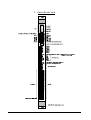
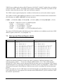
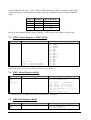
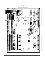
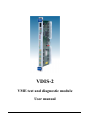
VDIS-2
VME test and diagnostic module
User manual
Wiener Plein & Baus Ltd. - 1/19/02
Seite: 1
Table of contents
1
GENERAL INFORMATION................................................................................................................................ 3
2
FRONT PANEL VIEW.......................................................................................................................................... 4
3
FUNCTIONAL DESCRIPTION........................................................................................................................... 5
3.1
3.2
3.3
3.4
3.5
3.6
4
REMARKS.............................................................................................................................................................. 9
4.1
4.2
4.3
5
MONITORING ................................................................................................................................................. 10
ADDRESS DATA -TESTS ................................................................................................................................. 10
DETECTION OF RANDOM BUS ERRORS ............................................................................................................ 10
BUS ALLOCATION TEST .................................................................................................................................. 10
INTERRUPT-DAISY-CHAIN CHECK.................................................................................................................. 11
UTILITY BUS CHECK ...................................................................................................................................... 11
SHORT MODE OPERATION............................................................................................................................ 12
6.1
6.2
7
GENERAL COMMENTS ...................................................................................................................................... 9
VDIS-2 TIMING ............................................................................................................................................... 9
POWER CONSUMPTION ..................................................................................................................................... 9
RECOMMENDATIONS FOR VDIS-2 USE...................................................................................................... 10
5.1
5.2
5.3
5.4
5.5
5.6
6
INTRODUCTION ................................................................................................................................................ 5
VME-BUS SIGNAL PROCESSING AND DISPLAY ................................................................................................. 5
OTHER LED’S .................................................................................................................................................. 6
VDIS-2 SWITCHES AND JUMPERS .................................................................................................................... 6
FRONT PANEL SWITCHES .................................................................................................................................. 7
INTERNAL SWITCHES ....................................................................................................................................... 8
SHORT MODE CONFIGURATION .................................................................................................................... 12
ACCESS TIMES................................................................................................................................................ 12
SHORT MODE ADDRESS MAP ....................................................................................................................... 13
7.1
7.2
7.3
7.4
7.5
7.6
CONTROL AND STATUS REGISTER (0X00) ....................................................................................................... 13
INTERRUPT AND TIMEOUT REGISTER (0X10) ................................................................................................. 14
VME CONTROL REGISTER + SOIC (0X20).................................................................................................... 15
VME ADRESS REGISTER (0X30).................................................................................................................... 15
VME DATA REGISTER (0X40) ....................................................................................................................... 15
TEST COUNTER (0X80) .................................................................................................................................. 16
8
VDIS-2 PCB LAYOUT ........................................................................................................................................ 17
9
VME-BUS REFERENCE .................................................................................................................................... 18
9.1
9.2
9.3
10
VME-BUS J1 CONNECTOR ............................................................................................................................. 18
VME-BUS J2 CONNECTOR ............................................................................................................................. 19
VME-BUS ADDRESS MODIFIERS ..................................................................................................................... 20
NOTES .................................................................................................................................................................. 21
Wiener Plein & Baus Ltd. - 1/19/02
Seite: 2
1
GENERAL INFORMATION
The new VDIS-2 is a new generation of the VDIS VME bus display and diagnostic module, which
has been successfully used in the VME applications in industry and research in the past 12 years.
VDIS-2 is a helpful tool for configuration, set-up and test of VME systems and software debugging
as well as for maintenance and service of VME hardware.
New features:
• VDIS2 is equipped with a 256 Byte VME-SHORT address area for extended test functions
fully programmable via VME
• Enlarged LED’s for better display
New VME-SHORT-area functions:
• Software control for all front panel switches
• Interrupt Logic for test purposes
• All addresses, data and VME-control lines are stored for each VME-cycle in a register for
read-back
• 32-bit data register for read and write tests
• 32-bit test counter.
VDIS2 standard features:
•
•
•
•
•
•
•
•
LED display for all relevant VME-bus lines:
Data Transfer Bus:
D00..D31, A00..A31, AM0..AM5, LWORD*, WRITE*
AS*, DS0*, DS1 *, DTACK*, BERR*.
Interrupt Bus:
IRQx*, IACK*, IACKIN*,IACKOUT*
Arbitration Bus:
BRx*, BGxIN* - BGxOUT*, BBSY*,BCLR*
Utility Bus:
SYSRESET*, SYSFAIL*, ACFAIL*, SYSCLK*.
Other:
+5Volt, +12Volt, -12Volt, VDIS-DTACK*,
EN-SHORT, VDis2-SELECT, EN-INTERRUPT, HALT
Can hold and keep visible signal groups with corresponding qualifier in certain conditions
(BERR, BBSY, DTACK, …)
Uses signal stretcher to increase visibility of signal groups and corresponding qualifier for
better display (IRQ, …)
VD (VDIS DTACK) diagnostic mode, VDIS-2 generates in case of a missing DTACK from
other VME units the DTACK at the end of a programmable „time-out“ time , in this mode
the data of the previous cycle are available for read-back ( VME READ only)
EH (ENABLE HALT) diagnostic mode, records the status of all VME bus signals in case of
a bus error and holds it until manual resetting
VDIS-2 is simply to use and transparent for any software.
VDIS is a standard 6U VME slave module
All main operating elements are accessible on the front panel. The display elements are
color coded functionally grouped.
Wiener Plein & Baus Ltd. - 1/19/02
Seite: 3
2
FRONT PANEL VIEW
VDIS2
Wiener Plein & Baus Ltd. - 1/19/02
Seite: 4
3
FUNCTIONAL DESCRIPTION
3.1 Introduction
VDIS displays most of the VMEbus signals with colored LED’s on the front panel. For easy
recognizing all address and data signals are arranged in four groups with different colors allowing a
fast transcriptionof the bit patterns into hexadecimal digits.
A shining LED shows an active signal. For example, the LED “D0” (Data 0) lights, if the signal on
this VME-bus line has a level higher than the TTL active threshold. Otherwise the LED „AS*“ is
on, if the signal on this VME-bus line has a level which is lower than the TTL switching threshold.
As described following in detail some of signals will be “captured” by the VDIS-2 logic or will be
elongated via “Stretcher” (signal elongation settings) to a visible duration. Some signals are
displayed staticly.
3.2 VME-bus Signal Processing and Display
The following signals are captured by a DTACK* or BERR* :
Data:
Addresses:
Address modifier:
Control signals:
Interrupt-Bus:
D00..D31
A01..A31
AM0..AM5
AS*, DS0*, DS1 *, WRITE*, LWORD*
IACK*, IACKIN*, IACKOUT*
In case of missing DTACK* or BERR*, the above listed bus signals are stored at the end of DS0* /
DS1*. This may cause a discrepancy between the stored data signals and the status of the VME
cycle if the address, data and AM hold times of the VME master are to short.
All control signals are displayed correctly in such cases because of storage in start registers.
The DTACK* und BERR* signals are “on activity” stored and displayed.
The following signals are captured with BBSY*:
Arbitration-Bus:
BG0IN*, BG0OUT*, BG1IN*, BG1OUT*
BG2IN*, BG2OUT*, BG3IN*, BG3OUT*
The following signals are stretched to be visible:
Interrupt-Bus:
Arbitration-Bus:
Utility-Bus:
Wiener Plein & Baus Ltd. - 1/19/02
IRQ1*..IRQ7 , IACK*, IACKIN*, IACKOUT*
BGx*, BRx*, BCLR*, BBSY*
SYSRESET*, SYSFAIL*, ACFAIL* ,BERR*
Seite: 5
SYSCLK* signal:
VDIS-2 detects the SYSCLK signal using a differential logic circuit. In a VME crate with multiple
master modules only one should be configured as system-controller. In case of more system
controllers on one bus the SYSCLK signal is fed multiple times to the bus. This can be indicated by
flashing CLK-LED’s. One of the VDIS-2 status bits further contains the information about the
presence of the SYSCLK signal.
3.3 Other LED’s
Power LED’s:
The power LED’s are indicating the presence of the correct voltages on the VME bus power lines
+5Volt, +l2Volt und -l2Volt. All voltages are monitored with a integrated circuit MAX 8215 with
the following thresholds:
• +5Volt-LED lights if U+5V > +4,6Volt.
• +l2Volt-LED lights if U+12V > +10,6 Volt.
• -l2Volt-LED lights if U-12V < -10,6 Volt.
It is assumed that +5V line used by the VDIS-2 is properly working. If not the case this may cause
wrong logic or display operations.
LED „VD“ (VDIS-DTACK):
VD indicates that VDIS-2 is working in a mode to generate DTACK* after the time-out period if no
other VME module generates this signal. The display is stretched to approximately 8 ms.
In case of an active HALT this LED lights permanently.
LED „INT“:
INT corresponds to an activated interrupt priority in the interrupt register. Pressing the switch
„INT“ an IRQx will be generated on the VME-bus.
LED „EN-SHORT“:
Displays that the VDIS-2 short address mode is switched on. The „EN-SHORT“ switch is located
on the PCB behind the front panel. In this mode SHORT calls are possible to program or to readout VDIS-2.
In a special mode this LED further indicates available data after the time-out in case of missing
DTACK (switches VD and EN-DATA = ON). This is shown by flashing (inverting) of the ENSHORT LED.
LED „HALT“:
The A00 address line does not exist on the VME-bus. Because of manufacturing reasons this LED
is equipped on the display and used to indicate a „HALT“ status by a short flashing of this LED (for
details see chapter 3.4).
Please note that the A00 LED is not labeled on the front panel.
The following bus lines are not displayed:
+5VSTBY, SERCLK, SERDAT* und RESERVED
3.4 VDIS-2 Switches and Jumpers
For easy operation the common used switches are located on the VDIS-2 front panel, i.e. there are 3
switches (VD, DA, EH) as well as 2 push-buttons (RH, INT) which are described following in
Wiener Plein & Baus Ltd. - 1/19/02
Seite: 6
detail. Further there are 2 internal switches located on the PCB behind the front panel ( SHORT /
ENABLE DATA modes). These switches have to be configured before inserting VDIS-2 into the
VME crate. The jumper array JA8 to JA15 defines the SHORT base address.
All other jumpers on the PCB are for future extensions and presently not used.
3.5 Front panel switches
„VD“ switch (VDIS-DTACK)
activates the “DTACK by VDIS-2” mode in which after a pre-defined time-out period VDIS-2
generates the DTACK signal on the VME-bus. The length of the time-out is fix 4µs (if „ENSHORT“ off). Using the VDIS-2 in the „EN-SHORT“ mode, this time can be programmed to be
either 3µs, 2µs or 1µs.
In the mode „VDIS-DTACK = ON“ VDIS-2 acts on all bus transfers which are not terminated
before the end of the time-out. This covers not only regular data transfers but also „interruptacknowledge-cycles“. Only in active „VD“ mode the „EN-DATA“ function can be used.
„DA“ switch (DISPLAY ALL)
enables the non-interpretive display mode. In case of „DA=OFF“ the signals of all bus transfers are
interpreted by the VDIS-2 logic for correct display. Thus a “Byte-transfer changes only the lower
byte of the display or in case of a16-bit short address cycle only the A01 - A15 and D00 - D15 are
displayed.
In “DA=ON“VDIS-2 shows all registered address, data and address modifier lines.
„EH“ switch (ENABLE HALT)
activates the “hold on error” mode. In case of a bus error all data, address and control signals will
be stored and displayed. The status of the “VD” will cause different actions in this mode:
1. “VD=ON”: in case of missing DTACK* from other VME units VDIS-2 generates the
DTACK* indicated by the shining red LED “VD“ and goes into the HALT mode shown by
the flashing “HALT“ LED.
2. “VD=OFF”: in case of missing DTACK* the BERR* will be generated on the VME-bus
followed by VDIS-2 going into the HALT mode which is shown by the flashing “HALT“
LED.
The hold state (HALT) can only be released by pushing the “RH“ button. This enables VDIS-2 to
detect the next bus error.
„RH“ button (RESET HALT)
releases VDIS-2 from the hold state (HALT) to an active ENABLE HALTmode.
„INT“ button (INTERRUPT)
sets the interrupt flip flop. The interrupt is only requested if an allowed interrupt-priority value
(1…7) is defined in the interrupt-register. In this case the LED „EN-INT“ lights.
A reset of the interrupt flip flop is only possible by software (SHORT MODE)
Wiener Plein & Baus Ltd. - 1/19/02
Seite: 7
3.6 Internal Switches
“EN-SHORT“ switch (ENABLE SHORT)
enables or disables the SHORT area of VDIS-2. In this mode several VDIS-2 functions as well as
the front panel switch configuration can be programmed. All addresses and functions are described
in detail in the following chapter.
“EN-DATA“ switch (ENABLE DATA)
If both „VD“ and „EN-DATA“ are switched on VDIS-2 transfers after the time out in case of a
read-cycle the content of the data register onto the VME-bus. Following a DTACK* will be
generated with a delay of about 30ns. In case of “EN-DATA+OFF” no data can be retrieved from
VDIS-2 except the SHORT READ for VDIS-parameters / features.
Wiener Plein & Baus Ltd. - 1/19/02
Seite: 8
4
REMARKS
4.1 General Comments
The VDIS-2 display does not disturb or affect the VME-bus or the functionality of any VME-bus
module except if used in one of the special diagnostic modes for trouble shooting.
VDIS-2 adds a TTL-LS-load to all VME-bus lines. The signals DTACK* and IRQx* have an
additional load of one 74LS641-1.
VDIS-2 bridges the “Daisy-Chain” lines BGxIN* to BGxOUT*. Similar bridges on the VME
backplane do not affect the VDIS-2 function.
ATTENTION !!! The signals IACKIN* and IACKOUT* have to be generated and to be
controlled by the VDIS2-Interrupt-logic circuit. The corresponding bridge on the VME
backplane has to be open!!!
VDIS-2 can be used in a crate with a 3U high J1 (P1) backplane only too. In this case all the signals
of the not present P2 (J2) bus Dl6..D31 and A24..A31 are in a non-defined state. Usually open lines
will be displayed as active ones.
Some older VME backplane do not have automatic daisy chain. In this case there may be slots with
not connected daisy chain lines. Using VDIS-2 in such a slot causes a non-defined state for these
signals which are then shown as non-active. However random distortions may occur
SYSRESET clears all displayed VME-bus data however SYSRESET*, SYSFAIL*, ACFAIL* und
SYSCLK are shown themselves.
4.2 VDIS-2 Timing
All addresses, data, address modifiers, IACK*, IACKOUT*, LWORD*, WRITE*, AS*, DS0* and
DS1 are in normal operation stored at the DTACK* or BERR* negation phase.
All signals are transferred with a nearly similar delay into the LATTICE-FPGA. For normal
operation a general set-up and hold time of at least 15ns is expected for all signals.
All VDIS-2 timing parameters are as specified within the „VME-bus Specification , ANSI/IEEESTD 1014-1987, IEC 821 and 297“ for VME-bus Slaves.
The VDIS-2 signal-stretcher can capture signals with a width of typically at least 10ns and display
them with visible extended length.
4.3 Power Consumption
Voltage Line
+5V
Maximum Current
1.1A to maximum 1.4 A
Wiener Plein & Baus Ltd. - 1/19/02
Power
max. 7 W
Seite: 9
5
RECOMMENDATIONS FOR VDIS-2 USE
5.1 Monitoring
For a permanent monitoring of the VME-bus activities VDIS-2 can be added to any VME system.
In this case “VD“ should be switched off. Depending on the required tasks “EH“ may be active.
Please note that some VME operating systems during initialization check the available address
space until the occurrence of the first bus error. Further there are VME block modes (CBLT
according to VME-P) which are terminated by a time-out. In these cases e detected bus error
represents a legal one.
As described following the position of VDIS-2 in the VME crate may allow different tests.
5.2 Address Data -Tests
It is possible to test the VME-bus data and address lines for disconnections or shortages by a cycle
with alternating write / read operations to different addresses in the “VD” mode.
Example:
i write: all even address and data bits are 1 (other 0)
i+1 write: all odd address and data bits are 1 (other 0)
In a continues cycle a homogeneously changing pattern has to be displayed, further it is
possible to read back addresses, data, address modifier and control signal for comparison with
the Software HALT function.
ATTENTION! Please make sure by selecting a suitable address modifier that no other slave
module in the VME system is accessed in such a test.
5.3 Detection of random bus errors
Operating VDIS-2 in the “EH“ mode allows to detect random bus errors even without using a
software debugger. These errors are usually caused by defective hardware or by incorrect software
code as “not initialized “ or “disapearing“ pointer. Even “spurious interrupts“ can be detected.
Some VME master generate only local bus errors. In these circumstances VDIS-2 can not detect a
VME-bus problem. If using VDIS-2 in the “VD“ and “EH“ mode however errors can be detected .
The time-out of the VME master has to be longer (> 5µs) than the VDIS-2 setting to allow to displa
the access address in case of a time out error.
5.4 Bus allocation test
For this purpose VDIS-2 has to be plugged into the slot before (to the left of) the VME master. In
this case the LED’s indicate how often the bus is allocated by the particular master or other ones of
the same priority level. This test can not be done for the VME-bus master with system controller
function which is located in slot “0“ of the VME crate.
Wiener Plein & Baus Ltd. - 1/19/02
Seite: 10
5.5 Interrupt-Daisy-Chain Check
Similar to the bus allocation test it is possible to get an indication about not responded or randomly
generated Interrupts by selecting the right slot number for VDIS-2 and enabled “EH“ mode.
Attention: The interrupt daisy-chain jumper has to be open!
5.6 Utility Bus Check
Failures are visible by looking to the relevant LED’s. Shortly occurring interferences on the
ACFAIL* line become visible due to the VDIS-2 signal stretching.
In case of multi master systems it is possible to detect a multiple inducted system clock SYSCLK
because of the overlay interference effects may occur shown by changing intensity of flashing of the
CLK-LED.
Wiener Plein & Baus Ltd. - 1/19/02
Seite: 11
6
SHORT MODE OPERATION
In addition to the front panel switches VDIS-2 has to internal switches for the EN-SHORT und ENDATA functions (see chapter 5.2).
To enable the SHORT-mode the EN-SHORT switch has to be in ON position and the jumper array
JA08 – JA15 has to be configured for the correct short base address.
PLEASE NOTE: The „EN-DATA“ switch / function is independent from the SHORT mode and
does not correspond to the SHORT data read.
6.1 SHORT mode configuration
VDIS-2 can be accessed in the SHORT address mode (AM = $29 or $2D) if “EN-SHORT=ON“.
The jumper array JA8 to JA15 defines the SHORT base address as following.
JA15 JA14 JA13 JA12 JA11 JA10 JA9
A15 A14 A13 A12 A11 A10 A9
:
I
I
I
:
I
I
: = Jumper open = logic 1
I = Jumper inserted = logic 0
JA08 Function
A8
VME-Short-address
I
Factory setting (0x8800)
The factory default VDIS-2 SHORT base address is $8800 (0x8800)
Important Notice: Please make sure that this address space is not otherwise used.
6.2 Access times
Write to VDIS-2:
Read from VDIS-2:
duration from AS* to DTACK*
duration from AS* to DTACK*
about 120ns.
about 120ns.
All data are available on the VME bus 60ns before DTACK*.
Wiener Plein & Baus Ltd. - 1/19/02
Seite: 12
7
SHORT MODE ADDRESS MAP
Short-Addres
+ Offset
Access Type
WR-Function /DATA
RD-Function /DATA
+ $80..FC
WORD
LWORD
BYTE
WORD
LWORD
Reset COUNTER
Reset COUNTER
DATA-Reg D07..D00/D15..D08
DATA-Reg D15..D00
DATA-Reg D31..D00
COUNTER Cnt15..Cnt00
COUNTER Cnt31..Cnt00
DATA-Reg D07..D00/D15..D08
DATA-Reg D15..D00
DATA-REG D31..D00
WORD
-
+ $20..2C
WORD
LWORD
Word
Software-Interrupt Control
AddrReg A23..A16
CLK- u. Power-Status
AddrReg A15..A1
AddrReg A31..A1
VME-Control-Signal Reg.
+ $10..1C
Word
+ $00..0C
Word
Interrupt Control Reg.
Timeout Reg.
Control Function
Interrupt Control Reg.
u. Timeout Reg.
STATUS Register
+
+
+
+
$40..7F
$40..7E
$40..7C
$32..
+ $30..3C
The VDIS-2 SHORT mode covers a 256 byte address space. The base address has to be defined by
the help of the jumpers JA8 ... JA15. The access to this area is only possible if “EN-SHORT=ON“.
LWORD calls to word addresses (A2 = 0) are possible however, the data bits D31 – D16 are not
relevant in this case.
7.1 Control and status register (0x00)
Short-Addr.+$00
WORD
WR-Control-Register
RD-STATUS-Register
D15
D14
D13
D12
D11
D10
D09
D08
D07
D06
D05
D04
D03
D02
D01
D00
D15
D14
D13
D12
D11
D10
D09
D08
D07
D06
D05
D04
D03
D02
D01
D00
–
=
=
=
=
=
=
SO-HALT
SO-ENDATA
SO-RH puls
SO-EH on
SO-DA on
SO-VD on
=
=
=
=
=
=
=
=
=
=
=
=
=
=
=
=
1 > CLPW OK / 0 = Error
Jumper J2 (for future function)
Jumper J1 (for future function
SW-ENDATA /Switch-ENDATA
SW-RH
/Switch-RH
SW-EH
/Switch-EH
SW-DA
/Switch-DA
SW-VD
/Switch-VD
SO-HALT
X
X
SO-ENDATA /Software-ENDATA
SO-RH
/Software-RW
SO-EH
/Software-EH
SO-DA
/Software-DA
SO-VD
/Software-VD
Data bit = 0 means off
Data bit = 1 means on / active
By the help of the control register VDIS-2 can be completely controlled via software, i.e. it is
possible to define the VDIS-2 switch settings and operation modes by the setting of the
corresponding bits D00 to D04 in the control register. Please note that the final function / mode is a
logic OR of the front panel switch state and the control register setting!
Wiener Plein & Baus Ltd. - 1/19/02
Seite: 13
VDIS-2 has an additional software HALT function “SO-HALT“ (bit D07) which allows to hold the
content of the data-, address- and VME control registers unchanged. This makes it possible to read
back the values from the previous VME cycle from these registers.
The VDIS-2 status register displays the condition of all switches as well as the software register.
The CLPW (CLOCK and POWER) bit indicates a correct VME environment and is determined in
the following way (AND , AND NOT are logic operators):
CLPW = (SCLKOK) AND (+5VOK) AND (+12VOK ) AND (-12VOK) AND NOT (+5VOV)
SCLKOK
+5VOK
+12VOK
-12VOK
+5VOV
= SYSCLK is active on VME backplane
= +5 Volt supply > +4,6Volt
= +12 Volt supply > + 10,6 Volt
= -12 Volt supply < – 10,6Volt
= +5 Volt supply > + 5,5 Volt (OVERVOLTAGE !)
The status of SCLKOK and the individual power line conditions are in addition stored in the VME
address register (offset 0x32, see paragraph 7.4).
7.2 Interrupt and Timeout Register (0x10)
Short-Adr.+$10
WORD
WR I.T. Register
RD I.T. Register
D15
D14
D13
D12
D10
D11
D10
D08
D07
D06
D05
D04
D03
D02
D01
D00
D15
D14
D13
D12
D10
D11
D10
D08
D07
D06
D05
D04
D03
D02
D01
D00
=
=
=
=
=
=
=
=
=
=
=
=
=
=
=
=
x
x
Timout (bit 1)
Timout (bit 0)
Interrupt-Mode 0=RORA/1=ROAC
Interrupt-Priority (bit 2)
Interrupt-Priority (bit 1)
Interrupt-Priority (bit 0)
Interrupt-Vector (bit 7)
Interrupt-Vector (bit 6)
Interrupt-Vector (bit 5)
Interrupt-Vector (bit 4)
Interrupt-Vector (bit 3)
Interrupt-Vector (bit 2)
Interrupt-Vector (bit 1)
Interrupt-Vector (bit 0)
=
=
=
=
=
=
=
=
=
=
=
=
=
=
=
=
0
0
Timout (bit 1)
Timout (bit 0)
Interrupt-Mode 0=RORA/1=ROAC
Interrupt-Priority (bit 2)
Interrupt-Priority (bit 1)
Interrupt-Priority (bit 0)
Interrupt-Vector (bit 7)
Interrupt-Vector (bit 6)
Interrupt-Vector (bit 5)
Interrupt-Vector (bit 4)
Interrupt-Vector (bit 3)
Interrupt-Vector (bit 2)
Interrupt-Vector (bit 1)
Interrupt-Vector (bit 0)
VDIS-2 has interrupt capability. In order to be able to generate a VME-bus interrupt a valid
interrupt priority ( value 1 …7) has to be defined within bits D08 – D11. This is indicated by a
shining “INT“ LED. In this case the interrupt flip flop becomes active by pressing the “INT“ button
on the front panel or by requesting an interrupt via software (please see paragraph 7.3 VME Control
and Software Interrupt Control Register). IRQx becomes active according to the defined interrupt
priority.
Please note, that in case of a VME master activated interrupt the corresponding interrupt vector has
to be loaded first. For a description of the interrupt mode (RORA/ROAC) please consult the VME
bus manual / specification.
Wiener Plein & Baus Ltd. - 1/19/02
Seite: 14
In the VDIS-DTACK mode (“VD“ =ON) the VME bus display VDIS-2 generates the DTACK*
signal after time-out. The length of the time-out period is adjustable when working in SHORT
mode.
TO bit 1
0
0
1
1
TO bit 0
0
1
0
1
Time to DTACK*
4µs
3µs
2µs
1µs
In case of de-activated SHORT mode (“SHORT”=OFF) the time-out length is fixed to 4µs.
7.3 VME Control Register + SOIC (0x20)
Short-Adr.+$20
WORD
WR Softw. Interrupt Control (soic)
D15..D02 = x
D01 = 1 = Software Interrupt
D00 = 1 = Reset Interrupt-FF
RD VME-Contol-Register (creg)
D15
D14
D13
D12
D10
D11
D10
D08
D07
D06
D05
D04
D03
D02
D01
D00
=
=
=
=
=
=
=
=
=
=
=
=
=
=
=
=
IACK*
IACKIN*
IACKOUT*
DTACK*
BERR*
AS*
DS0*
DS1*
WRITE*
LWORD*
AM5
AM4
AM3
AM2
AM1
AM0
AM0..IACK* will be stored in every VME cycle except HALT or SO-HALT
7.4 VME Adress Register (0x30)
Short-Adr.+$30
WR VME-ADR-Register
RD VME-ADR-Register (areg)
D15..D00 = areg15..01,0
D31..D00 = areg31..01,0
--D15 = SCLKOK
(1 = SYSCLK aktiv)
D14 = +5V OK
(1 = U > +4,6 V)
D13 = +12V-OK
(1 = U > +10,6V)
D12 = -12V-OK
(1 = U > -10,6V)
D11 = +5V-OverVoltage (0 = U < +5,5 V)
D10..D08 = 0
D07..D00 = areg23..areg16
WORD
LWORD
--WORD (+$32)
A31..A01 will be stored in areg in every VME cycle except HALT or SO-HALT
7.5 VME Data Register (0x40)
Short-Adr.+$40
WR VME-DATA-Register
BYTE
WORD
LWORD
Wiener Plein & Baus Ltd. - 1/19/02
RD VME-DATA-Register (dreg)
D15..D00 = dreg15..00 / LB or HB
D15..D00 = dreg15..00
D31..D00 = dreg31..00
Seite: 15
D31..D01 will be stored in dreg in every VME cycle except HALT or SO-HALT
7.6 Test Counter (0x80)
Short-Adr.+$80
WR Counter
RD Counter (cnt)
WORD
LWORD
Clear Counter (data not used)
Clear Counter (data not used)
D15..D00 = cnt15..00
D31..D00 = cnt31..00
The content of cnt will be increased by 1 with each cnt read .
Wiener Plein & Baus Ltd. - 1/19/02
Seite: 16
8
Wiener Plein & Baus Ltd. - 1/19/02
VDIS-2 PCB LAYOUT
Seite: 17
9
VME-BUS REFERENCE
9.1 VME-bus J1 connector
P1 on the VME module is a male 96-pin DIN 41612 connector (style C) with 3 rows a, b and c:
PIN #
Row A
Signal Name
Row B
Signal Name
Row C
Signal Name
1
2
3
4
5
6
7
8
9
10
11
12
13
14
15
16
17
18
19
20
21
22
23
24
25
26
27
28
29
30
31
32
D 00
D 0l
D 02
D 03
D 04
D 05
D 06
D 07
GND
SYSCLK
GND
DS1*
DS0*
WRITE*
GND
DTACK*
GND
AS*
GND
IACK*
IACKIN*
IACKOUT*
AM 4
A 07
A 06
A 05
A 04
A 03
A 02
A 01
-12V
+5V
BBSY*
BCLR*
ACFAIL*
BGOIN*
BG0OUT*
BG1IN*
BG1OUT*
BG2IN*
BG2OUT*
BG3IN*
BG3OUT+
BR0*
BRl *
BR2*
BR3 *
AM 0
AM 1
AM 2
AM 3
GND
SERCLK
SERDAT*
GND
IRQ7*
IRQ6*
IRQS*
IRQ4*
IRQ3 *
IRQ2*
IRQ1*
+5V STBY
+5V
D 08
D 09
D 10
D 11
D 12
D 13
D 14
D 15
GND
SYSFAIL*
BERR*
SYSRESET*
LWORD*
AM 5
A 23
A 22
A 21
A 20
A 19
A 18
A 17
A 16
A 15
A14
A 13
A 12
A 11
A 10
A 09
A 08
+12V
+5V
Wiener Plein & Baus Ltd. - 1/19/02
Seite: 18
9.2 VME-bus J2 Connector
P2 on the VME module is a male 96-pin DIN 41612 connector (style C) with 3 rows a, b and c.
PIN #
Row A
Signal Name
Row B
Signal Name
Row C
Signal Name
1
2
3
4
5
6
7
8
9
10
11
12
13
14
15
16
17
18
19
20
21
22
23
24
25
26
27
28
29
30
31
32
N.C.
N.C.
N.C..
N.C.
N.C.
N.C.
N.C.
N.C.
N.C.
N.C.
N.C.
N.C.
N.C.
N.C.
N.C.
N.C.
N.C.
N.C.
N.C.
N.C.
N.C.
N.C.
N.C.
N.C.
N.C.
N.C.
N.C.
N.C.
N.C.
N.C.
N.C.
N.C.
+5V
GND
RESERVED
A 24
A 25
A 26
A 27
A 28
A 29
A 30
A 31
GND
+5V
D 16
D 17
D 18
D 19
D 20
D 21
D 22
D 23
GND
D 24
D 25
D 26
D 27
D 28
D 29
D 30
D 31
GND
+5V
N.C.
N.C.
N.C.
N.C.
N.C.
N.C.
N.C.
N.C.
N.C.
N.C.
N.C.
N.C.
N.C.
N.C.
N.C.
N.C.
N.C.
N.C.
N.C.
N.C.
N.C.
N.C.
N.C.
N.C.
N.C.
N.C.
N.C.
N.C.
N.C.
N.C.
N.C.
N.C.
N.C. = not connected on VDIS-2
All signals with ' * ' are active in case of a level below the TTL threshold.
Wiener Plein & Baus Ltd. - 1/19/02
Seite: 19
9.3 VME-bus address modifiers
Adress Modifier (hex) Funktion
3F
3E
3D
3C
3B
3A
39
38 .. 2E
2D
2C .. 2A
29
28 .. 20
1 F .. 10
0F
0E
0D
0C
0B
0A
09
08 .. 00
Standard Supervisory Block Transfer
Standard Supervisory Programm Access
Standard Supervisory Data Access
Reserved
Standard Nonprivileged Block Transfer
Standard Nonprivileged Programm Access
Standard Nonprivileged Data Access
Reserved
Short Supervisory Access
Reserved
Short Nonprivileged Access
Reserved
User-defined
Extended Supervisory Block Transfer
Extended Supervisory Programm Access
Extended Supervisory Data Access
Reserved
Extended Nonprivileged Block Transfer
Extended Nonprivileged Programm Access
Extended Nonprivileged Data Access
Reserved
Wiener Plein & Baus Ltd. - 1/19/02
Seite: 20
10 NOTES
Wiener Plein & Baus Ltd. - 1/19/02
Seite: 21