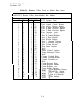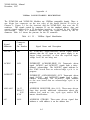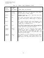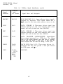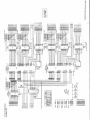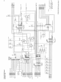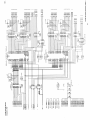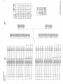
1
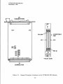
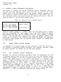
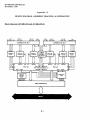
 XVME-200 / XVME-290
32-Channel Digital I/O Module
USER’S MANUAL
ACROMAG INCORPORATED
30765 South Wixom Road
P.O. BOX 437
Wixom, MI 48393-7037 U.S.A.
Tel: (248) 295-0885
Fax: (248) 624-9234
Email: [email protected]
Copyright 2012, Acromag, Inc., Printed in the USA.
Data and specifications are subject to change without notice.
8500-965B XVME-200/290 Manual
December, 1987
Chapter 1
INTRODUCTION
1.1
OVERVIEW
The XVME-200 and XVME-290 are Digital I/O VMEbus compatible boards (also
referred to as DIO Modules).
The XVME-200 is a single-high (3U), single-wide
module, and the XVME-90 is a double-high (6U), single-wide form factored modules.
The DIO Module provides a VME system with 32 digital (TTL) I/O channels, full
VMEbus interrupt capability, and port handshake control features. The DIO Module
utilizes two 68230 Parallel Interface/Timer Integrated Circuit devices (also referred
to as PI/T devices) to provide and control its parallel interface functions (with 16
I/O channels per PI/T device). In addition, the 68230 devices also provide two 240
bit, software-configurable timers (1 timer per PI/T device), which can be used to
generate periodic interrupts, a single interrupt after a specified time period, or a
square wave. The specific features of the DIO Module are listed below:
Direct compatibility with OPT0 22 -- 24 point subsystems, of either
single or quad density, with no transition interface required
(XVME-290/2).
--
Fully buffered TTL outputs, and hysteresis on TTL Inputs.
Software-configurable port direction (i.e., ports may be configured to
either input or output TTL level data).
Complete VMEbus interrupt capability (I( 1)-I(7)
--
interrupts - STAT).
Programmable IACK vector (with vector alteration based on the source of
the interrupt.
Port handshake signals are available to coordinate port data transfers.
TW O
24=bit,
software-configurable, timers.
The XVME-200 provides 32 digital I/O channels plus port handshake and timer
control signals through the VMEbus P2 connector. The XVME-290/2 places all
signals on OPT0 22 compatible connectors (JKI and JK2) located in the P2 area.
l-l
XVME-200/290 Manual
December, 1987
1.2 MANUAL STRUCTURE
This manual consists of three chapters which divide the various aspects of module
specification and operation into three distinct areas. The three chapters develop
these aspects in the following progression:
Chapter One - A general description of the XVME-200/290 Digital I/O Module,
including complete functional and environmental specifications, VMEbus compliance information, and a block diagram.
Chapter Two - DIO Module installation information covering module specific
system requirements, jumpers, and connector pinouts.
Chapter Three - Details covering functional addressing, interrupt enabling, and
programming
considerations/requirements.
The Appendices are designed to provide additional information in terms of the
backplane signal/pin descriptions, a block diagram and assembly drawing, and module
schematics.
NOTE
In order to fully document the complex versatility of the XVME-200/290 and the 68230 PI/T
device, a manual kit is being shipped with the
XVME-200/290 DIO Module (the manual kit is
referenced as XYCOM Part #74200-001).
This
kit consists of two parts: a *Motorola MC68230
Manual (c) (referenced as XYCOM Part
#74200-003), a n d a n XVME-200/290 M a n u a l
(referenced as XYCOM Part #74200-002.
It is recommended
that the user read
(completely) the 68230 Manual prior to reading
further in the XVME-200/290 Manual. After
becoming familiar with the 68230 and how it is
programmed, the user should then read the
remainder of the XVME-200/290 Manual to
become acquainted with module base addressing,
register access offsets,
interrupt
control,
handshake
control,
and
operational
mode/programming
constraints.
* MC68230 Parallel Interface/Timer Manual, (c)Motorola Inc., 1983
1-2
XVME-200/290 Manual
December, 1987
The DIO Module uses two 68230 Parallel Interface/Timer devices to provide a total
of 32 parallel I/O lines (16 lines per chip) arranged as four I/O ports (two 8 line
ports per chip), as well as 2 programmable timers (1 timer per chip).
Several
different operating modes can be programmed for the parallel ports and timers, to
provide a high degree of versatility and flexibility.
Each 68230 chip has two (8 line) I/O ports labeled as Port Al and Port Bl for PI/T
#l, and Port A2 and Port B2 for PI/T #2. The third Port on each PI/T chip (Port
C/Alternate Function) is configured as a group of dedicated control lines for
interrupt handling, timer operation, and data port direction.
Each of the four I/O ports is independently buffered by its own 8-bit data
transceiver. The data transceivers are all bidirectional, with their direction being
independently controlled by PC0 and PC1 of the Port D/Alternate Function lines on
each PI/T. The 8 data lines within each of the four PI/T I/O ports Al, A2, Bl,
and B2 must always be programmed for the same direction (i.e., because transceiver
data direction is programmed individually for each port and cannot be done on a
line-by-line basis). In order to avoid signal direction contention between a PI/T
Port and its data transceiver, the direction of the ports and transceivers must be
programmed in the proper order (documented in Chapter 2).
The DIO Module design allows each of the PI/T ports Al, Bl, A2, or B2 to be
individually programmed in either Port Mode 0 or Port Mode 1 (refer to the 68230
Manual for a description of Port Modes). In addition, any of the submodes within
Port Modes 0 and 1 may be utilized. There are 4 buffered handshake lines for each
PI/T chip which (depending on the operation mode selected and the position of
jumpers Jl and J3) can be used to provide interlocked handshake, pulsed handshake,
interrupt input (independent of data transfer), or general purpose single-line I/O.
Each PI/T chip also contains its own 24-bit timer capable of signaling event
occurrence by generating a periodic interrupt, an interrupt after timeout, or a
square wave output. The timer interrupt capability is enabled by using three of the
Port C/Alternate Function pins programmed to carry the Timer Interrupt functions
(i.e., Timer Interrupt enable, Timer input, and Timer output).
The module address decode logic allows the user to select (via 6 jumpers) any one
of 64 of the 1K boundaries in the Short I/O Address Space to be used as the
module base address.
The PI/T Internal Registers are accessible at specific
addresses offset from the selected module base address. Any of the 7 VMEbus
interrupt levels may be selected (via 3 jumpers) to facilitate interrupt generation,
and handling from any one of 4 interrupt sources on the module (i.e., PI/T #l port
interrupts, PI/T #2 port interrupts, PI/T #l timer interrupts, and PI/T #2 timer
interrupts). Each of the two PI/T chips is capable of producing 5 different IACK
vectors (one for the timer and four for the ports) for a total of ten different IACK
vectors per module.
On the XVME-200/290 the configuration of the PI/Ts differ only in whether their
I/O signals interface to JKl or JK2 (XVME-200, 1XVME-290/2) or which P2 pins the
I/O signals connect to (XVME-290/l), and the .jumper number which controls the
direction of H2, which must be distinct.
1-5
XVME-200/290 Manual *
December, 1987
1.4
MODULE
SPECIFICATIONS
The following is a list of the operational and environmental specifications for the
XVME-200/290 DIO Module.
1-6
XVME-200/290 Manual
December, 1987
Table l-l. Digital I/O Module Specifications
Specification
Characteristic
Number of Channels
32
Parallel
Interface
68230 (2 per module)
Input
Characteristics
Output
Power
Board
Device
Characteristics
Requirements
Dimensions
Temperature
Operating
Non-Operating
Humidity
Altitude
Operating
Non-Operating
Vibration
Operating
Non-Operating
Shock
Operating
Non-Operating
V il = 0.8V max., Iil = -750 uA max.
V ih = 2.0v min., lil= -325 uA max.
V ol = 0.4V max., Iol = 12 mA
V ol = 0.5V max., Iol = 24 mA
Voh = 2.4V min., Ioh = -3 mA
V oh = 2.0v min., Ioh = -15 mA
+5V, 1.3 A typ., 1.5 A max.
Single-height size (150 x 116.7 mm)(XVME-200)
Double-height size (160 x 233.4 mm)(XVME-290)
O” to 32' C (32O to 149OF)
-4OO to 85OC (-40° to 158OF)
5 to 95% RH non-condensing
(Extremely low humidity may require
protection against static discharge.)
Sea-level to 10,000 ft. (3048m)
Sea-level to 50,000 ft. (1524Om)
5 to 2000 Hz
0.015" peak-to-peak displacement
2.5 g peak acceleration
5 to 2000 Hz
0.030” peak-to-peak displacement
5.0 g peak acceleration
30
11
50
11
g peak acceleration
msec duration
g peak acceleration
msec duration
1-7
XVME-200/290 Manual
December, 1987
VMEbus Compliance
Complies with VMEbus Standard Rev. C.l
A 16:D8(0) DTB Slave
I(1) to I(7) interrupter (STAT) with
programmable interrupt vector
Size - Single (XVME-200
Size - Double (XVME-290)
Base address jumper-selectable on 1K
boundaries within the VMEbus short I/O
address space
l-8
XVME-200/290 Manual
December, 1987
Chapter 2
INSTALLATION
2.1
INTRODUCTION
This chapter explains how to configure the XVME-200/290 DIO Module prior to
installation in a VMEbus backplane. Included in this chapter is information on
module base address selection jumpers, module interrupt level selection jumpers, the
handshake line H2 direction jumpers, connector pinouts, and a brief outline of the
physical installation procedure.
2.2 SYSTEM REQUIREMENTS
The XVME-200/290 DIO Modules are VMEbus compatible modules. To operate, they
must be properly installed in a VMEbus backplane.
The minimum system requirements for the operation of an XVME-200/290 DIO
Modules are one of the following:
A host processor module properly installed on the same backplane as the
XVME-200/290; and a controller subsystem module which employs a Data
Transfer Bus Arbiter, a System Clock driver, a System Reset driver, and a
Bus timeout module. (The XYCOM XVME-010 System Resource Module
provides a controller subsystem with the components listed.)
--
OR
--
A host processor module which incorporates an on-board controller subsystem (such as XYCOM’s XVME-600 or XVME-601).
Prior to installing the XVME-200/290 DIO Modules, it will be necessary to configure
several jumper options. These options are:
1)
2)
3)
4)
2.3
Module base address within the short I/O address space.
Address Modifier codes to which the DIO Module will respond.
Interrupt level.
Direction of handshake line H2 on the 68230 PI/T chip.
XVME-200/290 DIO MODULE JUMPER/CONNECTOR LOCATIONS
The jumpers and connectors relevant to the installation of the XVME-200 DIO
Module are shown in Figure 2-1, and the jumpers and connectors relevant to the
installation of the XVME-290/2 DIO Module are shown in Figure 2-2, and Figure 2-3
shows the XVME-290/l.
2-1
XVME-200/290 Manual
December, 1987
2.4
XVME-200/290
DIO MODULE JUMPER LIST
Table 2-1. DIO Module Jumper List
Jumper
Use
Jl and J3
Determine the direction of handshake line H2 for both of the
PI/T chips (refer to Section 2.4.5 of this manual).
J2
Determines whether the module will respond to supervisory or
non-privileged short I/O VMEbus cycles (refer to Section 2.4.2
of this manual).
JAl0-JAI5
Select module base address on any one of the 64 1K boundaries
within the short I/O address space (refer to Section 2.4.1 of
this manual).
JA1-JA3
Select the VMEbus interrupt level for the module (refer to
Section 2.4.3 of this manual).
2.4.1
Base Address Jumpers
The DIO Module can be configured to be addressed at any one of the 64 IK
boundaries within the VME Short I/O Address space by using jumpers JAI0 through
JA15 (see Figure 2-1 (XVME-200), or Figure 2-2 (XVME-290) for the location of the
jumpers on the board) as shown below:
Table 2-2. Base Address Jumper Options
JA15
JA14
IN
IN
IN
IN
IN
IN
IN
IN
IN
IN
IN
IN
IN
IN
IN
IN
IN
IN
IN
IN
IN
IN
IN
IN
IN
IN
JA13
IN
IN
IN
IN
IN
IN
IN
IN
OUT
OUT
OUT
OUT
OUT
JA12
IN
IN
IN
IN
OUT
OUT
OUT
OUT
IN
IN
IN
IN
OUT
2-5
JAI1
IN
IN
OUT
OUT
IN
IN
OUT
OUT
IN
IN
OUT
OUT
IN
JAI0
IN
OUT
IN
OUT
IN
OUT
IN
OUT
IN
OUT
IN
OUT
IN
Base Address of
Module
OOOOH
0400H
0800H
OCOOH
1OOOH
1400H
1800H
1COOH
2000H
2400H
2800H
2COOH
3000H
XVME-200/290 Manual
December, 1987
Table 2-2. Base Address Jumper Options (Cont’d)
JA15
IN
IN
IN
IN
IN
IN
IN
IN
IN
IN
IN
IN
IN
IN
IN
IN
IN
IN
IN
OUT
OUT
OUT
OUT
OUT
OUT
OUT
OUT
OUT
OUT
OUT
OUT
OUT
OUT
OUT
OUT
OUT
OUT
OUT
OUT
OUT
OUT
OUT
OUT
OUT
OUT
JA14
IN
IN
IN
OUT
OUT
OUT
OUT
OUT
OUT
OUT
OUT
OUT
OUT
OUT
OUT
OUT
OUT
OUT
OUT
IN
IN
IN
IN
IN
IN
IN
IN
IN
IN
IN
IN
IN
IN
IN
IN
OUT
OUT
OUT
OUT
OUT
OUT
OUT
OUT
OUT
OUT
JA13
OUT
OUT
OUT
IN
IN
IN
IN
IN
IN
IN
IN
OUT
OUT
OUT
OUT
OUT
OUT
OUT
OUT
IN
IN
IN
IN
IN
IN
IN
IN
OUT
OUT
OUT
OUT
OUT
OUT
OUT
OUT
IN
IN
IN
IN
IN
IN
IN
IN
OUT
OUT
JA12
OUT
OUT
OUT
IN
IN
IN
IN
OUT
OUT
OUT
OUT
IN
IN
IN
IN
OUT
OUT
OUT
OUT
IN
IN
IN
IN
OUT
OUT
OUT
OUT
IN
IN
IN
IN
OUT
OUT
OUT
OUT
IN
IN
IN
IN
OUT
OUT
OUT
OUT
IN
IN
2-6
JAll
IN
OUT
OUT
IN
IN
OUT
OUT
IN
IN
OUT
OUT
IN
IN
OUT
OUT
IN
IN
OUT
OUT
IN
IN
OUT
OUT
IN
IN
OUT
OUT
IN
IN
OUT
OUT
IN
IN
OUT
OUT
IN
IN
OUT
OUT
IN
IN
OUT
OUT
IN
IN
JAlO
OUT
IN
OUT
IN
OUT
IN
OUT
IN
OUT
IN
OUT
IN
OUT
IN
OUT
IN
OUT
IN
OUT
IN
OUT
IN
OUT
IN
OUT
IN
OUT
IN
OUT
IN
OUT
IN
OUT
IN
OUT
IN
OUT
IN
OUT
IN
OUT
IN
OUT
IN
OUT
Base Address of
Module
3400H
3800H
3COOH
4000H
4400H
4800H
4COOH
5000H
5400H
5800H
5COOH
6OOOH
6400H
6800H
6COOH
7000H
7400H
7800H
7COOH
8OOOH
8400H
8800H
8COOH
9000H
9400H
9800H
9COOH
AOOOH
A400H
A800H
ACOOH
BOOOH
B400H
B800H
BCOOH
COOOH
C4OOH
C8OOH
CCOOH
DOOOH
D400H
D800H
DCOOH
EOOOH
E400H
XVME-200/290 Manual
December, 1987
Table 2-2. Base Address Jumper Options (Cont’d)
JA15
JA14
OUT
OUT
OUT
OUT
OUT
OUT
2.4.2
OUT
OUT
OUT
OUT
OUT
OUT
JAI3
JA12
OUT
OUT
OUT
OUT
OUT
OUT
IN
IN
OUT
OUT
OUT
OUT
JAI1
OUT
OUT
IN
IN
OUT
OUT
JAI0
IN
OUT
IN
OUT
IN
OUT
Base Address of
Module
E800H
EC00H
F000H
F400H
F8OOH
FC00H
Address Modifier Jumper
The DIO Module has one jumper that determines which Address Modifier Codes it
will respond to. This jumper is labeled as J2 (see Figure 2-1 for the jumper
location). Jumper J2 determines whether the module will respond to supervisory or
to non-privileged short I/O VMEbus cycles. When jumper J2 is in, the module will
respond to supervisory short I/O bus cycles only. When jumper J2 is out, the
module will respond to both non-privileged and supervisory short I/O bus cycles.
Table 2-3 shows the relationship between jumper J2 and the Address Modifiers.
Table 2-3. Addressing Options
Jumper J2
In
out
Address Modifier that the DIO
Module will respond to
(2DH) Supervisory Only
(2DH) Supervisory or (29H) Non-privileged
2-7
XVME-200/290 Manual
December, 1987
2.4.3
Interrupt Level Selection Jumpers
The DIO Module can either be configured to generate VMEbus interrupts at levels
1-7 or the module interrupt capability can be completely disabled. Table 2-4 shows
how jumpers JAI-JA3 are used to determine the interrupt level status for the DIO
Module.
Table 2-4. Interrupt Level Jumper Positions
JA3
JA2
JAl
Interrupt Level Selected
In
In
In
In
Out
Out
Out
Out
In
In
Out
Out
In
In
Out
Out
In
Out
IN
Out
In
Out
In
Out
None, VMEbus Interrupter disabled
Level 1
Level 2
Level 3
Level 4
Level 5
Level 6
Level 7
The modules are shipped from the factory with jumpers JAI, JA2, and JA3 installed.
NOTE
When the module is never required to generate interrupts,
JAl, JA2, and JA3 should all be installed to ensure that a
programming bug will not generate a VMEbus interrupt.
2.4.4
BGIN*/BGOUT*-IACKIN*/IACKOUT*
Daisy Chain
The Data Bus Arbitration signals BGIN*/BGOUT*
are not used by the DIO Module
and are hardwired together on the module to allow the Bus Arbitration Daisy Chain
to pass through the backplane slot occupied by the DIO Module. In each slot of
the VMEbus backplane there are set of jumpers which short the “IN” lines to the
“OUT” lines. Since the BGIN*/BGOUT* signals are already hardwired on the DIO
Module, it is not necessary to insert the corresponding jumper on the slot occupied
by the DIO Module. However, the IACKIN*/IACKOUT* signals are used by the DIO
Module and thus, the backplane jumper for these signals must not be installed in
the backplane slot occupied by the DIO Module.
2.4.5
Handshake Line H2 Direction Jumpers
The 68230 PI/T chips on the DIO Module can be programmed to operate in Modes 0
and 1 (refer to the 68230 Manual for mode explanation). Data transfers in these
modes can be controlled via the four handshake pins on each chip.
These
handshake pins are designed to be used in any of several different programmable
protocols (a thorough understanding of Modes 0 and 1, and their associated
submodes presented in the 68230 Manual is necessary in order to fully understand
the variety of protocols).
2-8
XVME-200/290 Manual
December, 1987
In these modes, the direction of two of the handshake pins (H2 and H4) should be
programmable. However, due to constraints in hardware design, pin H4 must always
be programmed as an output. Thus, pin H2 may be programmed as either an input
or an output depending on what type of handshake protocol is to be used. Jumpers
Jl and J3 (refer to Figure 2-1 (XVME-200) or Figure 2-2 (XVME-290) for the
location of these jumpers) are used in conjunction with the programmed direction of
pin H2 to determine whether the buffered handshake line H2 will be used as an
input or an output. Jumper Jl is used to control the direction of the PI/T #l - H2
line and Jumper J3 is used to control the direction of the PI/T #2 - H2 line.
NOTE
In order to prevent the possibility of signal contention
when using handshake protocol, pin H4 of a 68230 chip
must always be programmed as an output with the H4
interrupt disabled, and the programmed direction of pin
H2 must be consistent with the position of the
corresponding jumper (J1 or J3).
Table 2-5 shows the relationship between the position of jumpers Jl and J3 and the
direction of the buffered handshake line H2 for each of the PI/T chips.
Table 2-5. Handshake Line H2 Direction Jumpers
PI/T #I
Jumper JI
In
Out
PI/T #2
Jumper J3
Direction of the corresponding
H2 handshake lines.
In
Out
.
1
Input
Output
CAUTION
The module is factory-shipped with Jl and J3 installed.
Therefore, it will be necessary to remove the jumpers if
the PI/T H2 lines are to be programmed as outputs.
Failure to do so will result in signal contention.
2.5 CONNECTOR PIN ASSIGNMENTS
2.5.1
JKl and JK2 Connectors
The PI/T port data lines, port handshake lines, and timer I/O lines are all available
to the user at two 50-pin connectors located on the module front panel (refer to
Figure 2-1 (XVME-200) or Figure 2-2 (XVME-290)). The connectors are labeled JKl
and JK2. The two connectors have identical pinouts and differ only as to which
PI/T device they interface with. Connector JKl carries the signals pertaining to
PI/T #l and Connector JK2 carries the signals pertaining to PI/T #2.
2-9
XVME-200/290 Manual
December, 1987
The XVME-290 Module I/O interconnect is done via
(XVME-290/l) or through two 50-pin connectors (JKl
area (XVME-290/2). On the XVME-290/l, P2 carries
#1 and PI/T #2, while for the XVME-290/2, JKl carries
carries signals for PI/T #2.
P2 of the VMEbus backplane
and JK2) mounted in the P2
all the signals for both PI/T
signals for PI/T #l and JK2
NOTE
Connectors JKl and JK2 are directly compatible with
OPT0 22 24-point subsystems, flat cables can be connected directly from the XVME-200 and XVME-290/2 to
the OPT0 22 system without the need for a transition
interface.
Table 2-6 shows the pin assignments for Connectors JKl and JK2, the signal
direction with respect to the XVME-200 and the XVME-290/2 Modules, and the
corresponding OPT0 22 channel number.
2-10
XVME-200/290 Manual
December, 1987
2.5.2
Pl and P2 Connectors
Connectors PI and P2 are mounted at the rear edge of the board (see Figure 2-1).
The pin connections for Pl ( a 96-pin, 3-row connector) contains the standard
address, data, and control signals necessary for the operation of VMEbus-defined
NEXP modules. (The signal definitions and pin-outs for the connector are found in
Appendix A of this manual.) The Pl connector is designed to mechanically interface
with a VMEbus defined Pl backplane.
2.5.3
P2
Connector
XVME-290/l
The P2 connector is a standard VMEbus P2 backplane connector with 96-pins (3
(The pin-outs for the connector P2 are found in Appendix A of this
rows).
The P2 connector is designed to interface with a VMEbus defined P2
manual.)
backplane. The P2 connector has been modified slightly for the XVME-290/l (see
Table 2-7).
2-12
XVME-200/290 Manual
December, 1987
Table 2-7. Pin Assignment for P2 (XVME-290/l
ROW A
Pin #
Signal
ROW B
Pin #
Only)
ROW C
Signal
Pin #
Signal
P2C-1
P2C-2
P2C-3
P2C-4
P2C-5
P2C-6
P2C-7
P2C-8
P2C-9
P2C-10
P2C-11
P2C-12
P2C-13
P2C-14
P2C-15
P2C-16
P2C-17
P2C-18
P2C-19
P2C-20
P2C-2 1
P2C-22
P2C-23
P2C-24
P2C-25
P2C-26
P2C-27
P2C-28
P2C-29
P2C-30
P2C-3 I
P2C-32
GND
H2 OUT-l
GND
H3 IN-l
GND
PB7-1
GND
PB4- 1
GND
PBI-1
GND
PA6- 1
GND
PA3-1
GND
PAO- I
GND
H2 OUT-2
GND
H3 IN-2
GND
PB7-2
GND
PB4-2
GND
PBl-2
GND
PA6-2
GND
PA3-2
GND
PAO-2
I
P2A-1
P2A-2
P2A-3
P2A-4
P2A-5
P2A-6
P2A-7
P2A-8
P2A-9
P2A-IO
P2A-I 1
P2A-12
P2A-13
P2A-14
P2A-I 5
P2A-16
P2A-17
P2A-18
P2A-19
P2A-20
P2A-2 1
P2A-22
P2A-23
P2A-24
P2A-25
P2A-26
P2A-27
P2A-28
P2A-29
P2A-30
P2A-3 1
P2A-32
H4 OUT-1
TMR OUT-1
H2 IN-l
Hl IN-1
TMR IN-1
PB6- 1
PB5-1
PB3- 1
PB2-1
PBO- 1
PA7-1
PAS-1
PA4- 1
PA2- 1
PAL1
GND
H4 OUT-2
TMR OUT-2
H2 IN-2
Hl IN-2
TMR IN-2
PB6-2
PB5-2
PB3-2
PB2-2
PBO-2
PA7-2
PA5-2
PA4-2
PA2-2
PAl-2
GND
P2B-1
P2B-2
NO
NO
NO
NO
NO
NO
NO
NO
NO
P2B-12
P2B-13
NO
NO
NO
NO
NO
NO
NO
NO
P2B-22
NO
NO
NO
NO
NO
NO
NO
NO
P2B-3 1
P2B-32
vcc
GND
CONNECT
CONNECT
CONNECT
CONNECT
CONNECT
CONNECT
CONNECT
CONNECT
CONNECT
GND
vcc
CONNECT
CONNECT
CONNECT
CONNECT
CONNECT
CONNECT
CONNECT
CONNECT
GND
CONNECT
CONNECT
CONNECT
CONNECT
CONNECT
CONNECT
CONNECT
CONNECT
GND
vcc
2-13
XVME-200/290 Manual
December, 1987
2.6 MODULE INSTALLATION
XYCOM XVME modules are designed to comply with all physical and electrical
VMEbus backplane specifications. The XVME-200 DIO Module is a single-high,
single-wide VMEbus module, and as such, only requires the Pl backplane. The
XVME-290/l DIO Module uses the P2 of the VMEbus backplane, or through the two
50 pin connectors (JKl and JK2) mounted in the P2 area (XVME-290/2). In the
XVME-290/l version, P2 carries all the signals for both PI/T #I and PI/T #2, while
the XVME-290/2 version, JKl carries the signals for PI/T #l and JK2 carries the
signals for PI/T #2.
CAUTION
Never attempt to install or remove any boards before
turning off the power to the bus, and all related external
power supplies.
Prior to installing a module, you should determine and
verify all relevant jumper configurations, and all
connections to external devices or power supplies. (Please
check the jumper configuration against the diagrams and
lists in this manual.)
To install a board in the cardcage, perform the following steps:
1)
Make certain that the particular cardcage slot which you are going to use
is clear and accessable.
2)
Center the board on the plastic guides in the slot so that the handle on
the front panel is towards the bottom of the cardcage.
3)
Push the card slowly toward the rear of the chassis until the connectors
engage (the card should slide freely in the plastic guides).
4)
Apply straight-forward pressure to the handle located on the front panel
of the module until the connector is fully engaged and properly seated.
NOTE
It should not be necessary to use excessive pressure or
force to engage the connectors. If the board does not
properly connect with the backplane, remove the module
and inspect all connectors and guide slots for possible
damage or obstructions.
2-14
XVME-200/290 Manual
December, 1987
5)
Once the board is properly seated, it should be secured to the chassis by
tightening the two machine screws at the extreme top and bottom of the
board.
2-15
XVME 200/290 Manual
December, 1987
Chapter 3
MODULE PROGRAMMING
3.1
INTRODUCTION
This chapter will briefly examine the addressing, and initialization procedures and
constraints required when programming the XVME-200 and XVME-290 DIO Modules.
In order to demonstrate the correct sequence of initialization for the ports and
registers contained in the 68230 PI/T chips, two programming examples (with
comments) have been incorporated in this chapter. For a complete explanation on
how to program and maximize the functionality of the 68230 PI/T chip, refer to the
accompanying 68230 Manual.
3.2 MODULE ADDRESSING
The XVME-200 and XVME-290 DIO Modules are designed to be addressed within the
VMEbus-defined 64K short I/O address space. When the DIO Module is installed in
the system it will occupy a 1K byte block of the short I/O address space. The base
address decoding scheme for the XVME I/O modules is such that the starting
address for each board resides on a 1K boundary.
Thus, there are 64 possible
locations (1K boundaries) in the short I/O address space which could be used as the
base address for the DIO Module (refer to Section 2.4.1 for the list of base
addresses and their corresponding jumper configurations).
The logical registers/ports utilized for the transfer of data on the XVME-200 and
XVME-290 Modules are all contained within the 68230 PI/T devices. All register
locations within the 68230 devices are given specific addresses which are offset
from the module base address (Table 3-1 lists the offsets specified for the registers
used in the 68230 chips).
3-1
XVME-2001290 Manual
December, 1987
Table 3-l. Register Offsets From the Module Base Address
68230 PI/T Register Offsets from Module Base Address
PI/T #l
DEC HEX
1
3
5
7
9
11
13
15
17
19
21
23
25
27
29
31
33
35
37
39
41
43
45
47
49
51
53
55
57
59
61
63
1
3
5
7
9
B
D
F
11
13
15
17
19
1B
1D
1F
21
23
25
27
29
2B
2D
2F
31
33
35
37
39
3B
3D
3F
PI/T #2
DEC HEX
65
67
69
71
73
75
77
79
81
83
85
87
89
91
93
95
97
99
101
103
105
107
109
111
113
115
117
119
121
123
125
127
41
43
45
47
49
4B
4D
4F
51
53
55
57
59
5B
5D
5F
61
63
65
67
69
6B
6D
6F
71
73
75
77
79
7B
7D
7F
/
PI/T Register Name
Port General Control Register
Port Service Request Register
Port A Data Direction Register
Port B Data Direction Register
Port C Data Direction Register
Port Interrupt Vector
Port A Control Register
Port B Control Register
Port A Data Register
Port B Data Register
Port A Alternate Register
Port B Alternate Register
Port C Data Register
Port Status Register
Null
Null
Timer Control Register
Timer Interrupt Vector
Null
Counter Preload High
Counter Preload Middle
Counter Preload Low
Null
Count Register High
Count Register Middle
Count Register Low
Timer Status Register
Null Registers Always
Read Zero. Writing
To A Null Register
Has No Effect On
The Module.
3-2
XVME-200/290 Manual
December, 1987
A specific register address in one of
adding the specific register offset to
offset specified for the Port General
the module base address is jumpered
1041H.
the 68230 chips can be accessed by simply
the module base address. For example, the
Control Register for PI/T #2 is 41H, and if
to 1000H, the register can be accessed at
Module Base Address
Register Offset
1000H
41H
PCG Register #2
=
1041H
NOTE
The XVME-200/290 are an odd byte only slave, and
as such, the module will not respond to even
However, word
address, single-byte
accesses.
accesses may be used, with the understanding that
only the odd byte of the word is used to exchange
data. If word accesses are used, the register offsets
listed in Table 3-l would all be decremented by 1.
Figure 3-l shows a simple map of the 1K block of the short I/O address space
which is occupied by the XVME-200/290 Modules.
EVEN
ODD
Base + 00H
3EH
40H
0lH
U
N
U
S
3FH
41H
E
D
7EH
80H
7FH
81H
Unused
3FEH
3FFH
Figure 3-1. Memory Map of the XVME-200 and XVME-290 Modules
3-3
XVME-200/290 Manual
December, 1987
3.3
MODULE VMEbus INTERRUPT CAPABILITY
Four sources of interrupts exist on the XVME-200 and the XVME-290. These are
the timer and port interrupt sources from both PI/T #l and PI/T #2. When
enabled, each of the four interrupt sources can generate VMEbus interrupts on the
level selected by jumpers JAI-JA3 (refer to Section 2.4.3 of this manual). The four
local interrupt sources are prioritized during the VMEbus IACK cycle. Table 3-2
shows the priority of the four local interrupt sources.
Table 3-2. Priority of Local Interrupt Sources
PI/T
PI/T
PI/T
PI/T
#l
#2
#l
#2
Highest Priority
Port Interrupt
Port Interrupt
Timer Interrupt
Timer Interrupt Lowest Priority
When the module responds to a VMEbus IACK cycle, the IACK vector is acquired
from the corresponding PI/T vector register (refer to the 68230 Manual for location
and operation) and driven onto the VMEbus. Each PI/T device produces 5 different
vectors, 4 from the ports and 1 from the timer. Thus, ten different VMEbus IACK
vectors can be provided by the XVME-200 and XVME-290 Modules. The appropriate
PI/T IACK vector registers must be initialized before interrupts are enabled (refer
to 68230 Manual).
3.3.1
Module VMEbus Interrupt Enabling
As mentioned in the previous section, the ports and timer of both PI/T devices have
the capability of generating VMEbus interrupts. The following subsections explain
the general procedure for enabling the port and timer interrupts.
3.3.1.1
Port
C/Alternate
Function
Initialization
Basically, the interrupt initialization procedures begin by programming the Port
C/Alternate function lines on the PI/T devices to carry the interrupt control
functions. The operation of the Port C/Alternate function lines is covered in depth
in the 68230 Manual, however, for the sake of clarity Figure 3-3 is included in this
manual.
Figure 3-3 defines the Port C/Alternate function lines and their
programmed direction for primary module use. Notice that some of the pins retain
the possibility of being used as Port C single-bit inputs/outputs if the module
interrupt and timer capabilities are not being used (i.e., pins 1 and 3), while others
must be dedicated to module control functions (i.e., pins 0 and 1 should always be
programmed as outputs to control the direction of the Port A and B data buffers,
and pins 4, 5, 6, and 7 are dedicated to timer and port interrupt control).
3-5
XVME-200/290 Manual
December, 1987
1
7
1
6
PC7/TIACK
Input
5
PC6/PIACK
Input
PIRQ
output
4
TINTEN
output
3
PC3/TOUT
output
2
PCZ/TIN
Input
1
PORT B
output
0
PORT A
output
Figure 3-3. Port C/Alternate Function Signal Definitions
The following is a brief explanation of each PORT C bit:
Bits
0 and 1 are used to control the direction of the 8-bit data
transceivers which are used to buffer the Port A and Port B data
lines. After start-up or reset, these bits should be programmed as
outputs.
Bit
2 is used as a timer input line if the 68230 timer function is being
utilized. If the timer function is not being used, this bit could be
employed as a general purpose input line.
.
Bit
3 is used as a timer output line if the 68230 timer function is being
utilized. If the timer function is not being used, this bit could be
employed as a general purpose output line.
l
Bit
4 is used as a timer interrupt enable line of the 68230 timer
function is being utilized. This bit can only be used for the timer
interrupt function.
.
Bit
5 is used as a port interrupt request line if the 68230 port
interrupts are enabled. This bit can only be used for the port
interrupt function.
l
Bit
6 is used as a port interrupt acknowledge line if the 68230 port
interrupts are enabled. This bit can onlv be used for the port
interrupt function.
.
Bit
7 is used as a timer interrupt acknowledge line if the 68230 timer
functions are being utilized. This bit can only be used for the
timer interrupt function.
3-6
XVME-200/290 Manual
December, 1987
During a VMEbus reset, all three PI/T ports (A, B, & C) assume an input direction.
Pull-up resistors present on bits PC0 and PC1 cause the port A and B data line
transceivers to assume an input direction. Pull-up resistors also cause PORT C pins
3, 4, and 5 to go high at reset, thereby preventing the possibility of unintentional
interrupts (port or timer). After reset, PORT C can be configured to conform to
the users needs (i.e., Port A and B transceiver direction, port and timer interrupt
control signals and timer I/O lines, and/or single-bit general purpose I/O). Figure
3-2 shows the direction for each PORT C pin as dictated by hardware configuration.
Some attention should be given to the possibility of generating
unintentional interrupts when configuring the direction of the PORT C pins. The
following procedure is an example of how PORT C could be initialized to appear as
it does in Figure 3-2.
1)
Write FFH to the PORT C Data register. This ensures that all PORT C pins
will be high when the direction of the pins is switched, thereby preventing the
possibility of unintentional interrupts (both port and timer) being generated.
2)
Write 1BH to the PORT C Direction register. This will configure the direction
of PORT C as shown in Figure 3-2, with the exception of pin 5 (PIRQ), which
remains an input to ensure that port interrupts will not be generated
unintentionally.
3)
Individual PORT C bits can now be programmed to conform to the user’s
needs. At this point, port interrupts could be enabled by merely programming
the PC6/PIACK and PC5/PIRQ pins to support the interrupt and acknowledge
functions.
3.3.1.2
PI/T Port Interrupt Enabling
In order to enable the PI/T port interrupt capability PORT C must be programmed
so that pins PC5/PIRQ a n d PC6/PIACK serve the port interrupt request and
acknowledge
functions. As such, the individual internal enable bits for Hl, H2, and
H3 determine whether a particular port function will generate a VMEbus interrupt.
NOTE
Handshake line H4 must be programmed as an output, and
H4 interrupts must always be disabled.
When H2 interrupts are to be used, input pin H2 must be physically jumpered to
configure the line for inputs (refer to Section 2.4.5 of this manual for H2 jumper
definitions). During the interrupt service routine, the “Direct Method” of clearing
the Hl, H2, or H3 status bits must be used to negate the interrupt (refer to the
68230 Manual for the “Direct Method” of clearing status bits).
3-7
XVME-200/290 Manual
December, 1987
3.3.1.3
PI/T Timer Interrupt Enabling
68230 timer interrupts are enabled/disabled via PORT C output pin PC4. When PC4
is negated (logic ‘l”), the timer cannot generate VMEbus interrupts. When PC4 is
asserted (logic “0”), the timer will generate VMEbus interrupts.
When the timer interrupts are to be used, PORT C pins PC3/TOUT and PC7/TIACK
must be programmed to serve the timer interrupt request and acknowledge functions.
Pin PC4 is then used to determine whether timer interrupts are enabled or disabled.
All interrupt related PORT C pins are connected to pull-up resistors, SO that when
the module is reset all PORT C lines will be configured as inputs and thus, all
module interrupts will be disabled.
During the interrupt service routine, the ‘Direct Method” must be used for clearing
the timer zero detect status bit in order to negate the interrupt (refer to the 68230
Manual for information on the “Direct Method” of clearing the timer).
a
When the timer interrupts are not going to be used, pin PC4 must be negated (logic
“1’) in order to disable timer interrupts. In these cases, pin PC3/TOUT can be
programmed either as a simple timer output or as a general purpose PORT C output
line.
3.4
PI/T PORT A AND PORT B DATA LINES
The I/O lines connected to the PI/T I/O pins are labeled PA0-PA7 and PB0-PB7
(refer to Figure 1-1 of this manual). The PORT A and B data lines are independently buffered by 8-bit transceivers. The 8 I/O lines assigned to each port must
all assume the same direction. Thus, all I/O lines in PORT A must assume the same
direction, and all the data lines in PORT B must assume the same direction. PORTS
A and B may however, assume different directions.
The direction of the 8-bit data transceivers which buffer each port is programmed
independent of the direction of the PORT I/O lines on the PI/T chips. The
direction of the data transceivers is programmed via the PORT C outputs PCO and
PCl. The state of the P CO and PC1 outputs should be programmed to be consistent
with the programmed direction of the PI/T ports.
When programming a port for output the direction of the transceiver and the port
should be set in the following sequence:
1)
2)
Set the direction of the data transceiver.
Set the direction of the PI/T Port.
When programming a port for input the direction of the port and transceiver should
be set in the following sequence:
1)
2)
Set the direction of the PI/T Port.
Set the direction of the data transceiver.
3-8
XVME-200/290 Manual
December, 1987
Table 3-3 shows how pins PC0 and PC1 affect the direction of the PORT A and B
data transceivers. Remember, each PI/T chip has its own PORT A and B, and thus
there is a total of 4 lines which are used to control the direction of the four data
transceivers (refer to the Module Block Diagram, Figure l-l).
Table 3-3. PORT A and B Data Transceiver Direction Control *
\
PC0 output
PC1 output
0
1
0
1
Data Line Transceiver Direction I
PA0-PA7 are OUTPUTS
PA0-PA7 are INPUTS
PB0-PB7 are OUTPUTS
PB0-PB7 are INPUTS
* These directions are the same for both PI/T chips.
CAUTION
PI/T pins PA0-PA7 must all be programmed to
assume the same direction, this direction must be
consistent with PC0 as shown in Table 3-3. PI/T
pins PBO-PB7 must all be programmed to assume the
same direction, this direction must be consistent with
PC1 as shown in Table 3-3. Failure to observe these
conventions will cause signal contention.
3.4.1
Port A and B Reset State
During a VMEbus reset, PI/T PORTS A, B, and C all assume an input direction.
Therefore, I/O signals PAO-PA7 and PBO-PB7 all assume an input direction during a
reset. This means that if the I/O signals are being used in an application as
outputs, they will have a “high” reset state. Thus, active “low” outputs would have
to be used on lines which must be negated on power-up or system reset. The
receivers of these active “low” outputs should limit their 1, value below 250uA to
guarantee that they will be negated upon reset.
3-9
XVME-200/290 Manual
December, 1987
3.5
PROGRAMMKNG
EXAMPLES
The two 68000 CPU code programming examples which follow, demonstrate general
methods of initialization of the 68230 PI/T devices on the XVME-200 and XVME-290
Modules. The following equates will be used in both examples:
; Interrupt vectors.
PVCTR
TVCTR
EQU $___ ; Port interrupt vector.
EQU $___ ; Timer interrupt vector.
; Values to preload counter.
CHIGH
EQU $____ ; High byte.
CMID
EQU $___ ; Middle byte.
CLOW
E Q U $___ ; Low byte.
; 68230 Base Address and Register Offsets.
; XVME-200 Module base address
(jumper selectable).
PI/TlBASEQU BASE200 + $00; 68230 PI/T #l base address.
PI/T2BASEQU BASE200 + $40; 68230 PI/T #2 base address.
BASE200 EQU $
PCDR
PSR
TCR
EQU $01
EQU $03
EQU $05
EQU $07
EQU $09
EQU $OB
EQU $OD
EQU $OF
EQU$ll
EQU $13
EQU $15
EQU $17
EQU $19
EQU $lB
EQU $21
TIVR
EQU $23
CPRH
CPRM
CPRL
EQU $27
EQU $29
EQU $2B
EQU $2F
EQU $31
EQU $33
EQU $35
PCGR
PSRR
PADDR
PBDDR
PCDDR
PIVR
PACR
PBCR
PADR
PBDR
PAAR
PBAR
CNTRH
CNTRM
CNTRL
TSR
;
;
;
;
;
;
;
;
;
;
;
;
;
;
;
;
;
;
;
;
;
;
;
Port general control register.
Port service request register.
Port A data direction register.
Port B data direction register.
Port C data direction register.
Port interrupt vector register.
Port A control register.
Port B control register.
Port A data register.
Port B data register.
Port A alternate register
Port B alternate register.
Port C data register.
Port status register.
Timer control register.
Timer interrupt vector register.
Counter preload register - high byte.
Counter preload register - mid byte.
Counter preload register - low byte.
Count register - high byte.
Count register - mid byte.
Count register - low byte.
Timer status register.
3-10
XVME-200/290 Manual
December, 1987
E x a m p l e #l *
Basic Set Up:
.
PI/T #l
Mode 0 = Unidirectional 8-bit Mode
Submode 1X = Bit I/O (Pin-Definable Single-Buffered Output or Non-Latched
Input)
Goals:
Port A, all bits = non-latched inputs.
1)
Port B, all bits = single buffered outputs.
2)
Port C, bit 0 = single buffered output (controls the direction of the
3)
transceiver connected to Port A).
Port C,
bit 1 = single buffered output (controls the direction of the
4)
transceiver connected to Port B).
Port C, bit 2 = non-latched input.
5)
Port C, bit 3 = single-buffered output (high).
6)
Port C, bit 4 = single-buffered output (programmed high to disable timer
7)
interrupts).
Port C, bit 5 = PIRQ* function.
8)
Port C, bit 6 = PIACK* function.
9)
10) Port C, bit 7 = non-latched input (will always read as one).
11) The handshake pins (Hl,H2,H3,H4) are at a low voltage level when negated,
and at a high voltage level when asserted.
12) Hl is an edge-sensitive status input, HlS is set by an asserted edge of Hl.
13) H2 is a negated output pin and H2S is always cleared.
14) H3 is an edge-sensitive status input, H3S is set by an asserted edge of H3.
15) H4 is an asserted output pin and H4S is always cleared.
16) All interrupts are disabled.
17) The timer is disabled.
l
CODE:
M0VEA.L # PI/TlBASE,AO
; A0 = base address of PI/T #l
M0VE.B #$FF,PCDR(AO)
M0VE.B #$l B,PCDDR(AO)
;
;
;
;
;
;
M0VE.B
; Port mode = 0
; H34,H12 interrupts disabled
; Handshake pins = active high
#$OF,PGCR(AO)
MOVE.B #$AO,PACR(AO)
;
;
;
;
Initialize Port C control
functions
Port A ‘& B transceivers = output
PC3/TOUT = high
PC4 = high (timer interrupts disabled)
PC7,6,5,2 = inputs
Initialize Port A
Submode 1X
H2 = negated output
HI & H2 interrupts disabled
3-11
XVME-200/290 Manual
December, 1987
M0VE.B
#$AS,PBCR(AO)
;
;
;
;
M0VE.B
#$18,PSRR(AO)
; PC4 = Port C function
; PCS/PIRQ = PIRQ function
; PC6/PIACK = PIACK function
M0VE.B #O,PADDR(AO)
M0VE.B #$FF,PBDDR(AO)
BCLR
#O,PCDR(AO)
M0VE.B
#O,TCR(AO)
;
;
;
‘;
Initialize Port B
Submode 1X
H4 = asserted output
H3 & H4 interrupts disabled
Set Port A & B direction
Port A = input mode
Port B = output mode
Port A transceiver = input mode
; PC2, PC3 & PC7 = Port C function
; timer disabled
After this initialization code is executed, PI/T #1 Port A data register will reflect
the state of PA7-1 through PAO-I. Data written to PI/T #I Port B will appear on
PB7-1 through PBO-I.
Example #2
Basic Set Up:
PI/T #2
Mode 1 = Unidirectional 16-bit Mode
Submode X l = Pin-Definable Double-Buffered Output or Non-Latched Input
Goals:
Port A and B, all bits = double buffered outputs.
1)
Port C, bit 0 = single buffered output (controls the direction of the
2)
transceiver connected to Port A).
Port C, bit 1 = single buffered output (controls the direction of the
3)
transceiver connected to Port B).
Port C, bit 2 = TIN function. The prescaler will not be used. The signal TIN
4)
will be used to decrement the counter.
Port C, bit 3 = TOUT function.
5)
Port C, bit 4 = single-buffered output (controls the timer interrupt enable).
6)
Port C, bit 5 = PIRQ* function.
7)
Port C, bit 6 = PIACK* function.
8)
Port C, bit 7 = TIACK* function.
9)
10) The handshake pins (Hl,H2,H3,H4) are at a low voltage level when negated,
and at a high voltage level when asserted.
11) Hl is an edge-sensitive input, HIS is set by an asserted edge of Hl, and Hl
interrupt is enabled.
12) H2 is an edge-sensitive input, and H2S is set by an asserted edge of H2, and
H2 interrupt is disabled.
13) H3 and H4 set up for interlocked output handshake protocol.
14) H4 interrupt is disabled.
15) Timer is set up to interrupt after timeout (and started).
3-12
XVME-200/290 Manual
December, 1987
16) Vectored interrupts are supported.
17) When zero is detected, the counter will generate a VMEbus interrupt, reload
the counter, and continue counting.
18) Hl, H2, H3, and timer interrupts are enabled.
CODE:
M0VEA.L #PI/T2BASE,AO
M0VE.B #O,TCR(
AO)
M0VE.B #$FF,PCDR(AO)
M0VE.B #$l B,PCDDR(AO)
.
3
.
9
;
.
9
;
;
;
M0VE.B
#$4F,PGCR(AO)
.
3
.
9
;
M0VE.B
#$06,PACR(AO)
;
;
;
;
M0VE.B
#$32,PBCR(AO)
;
;
;
M0VE.B
#$18,PSRR(AO)
;
.
9
.
9
MOVE.B
M0VE.B
#$FF,PADDR(AO)
#$FF,PBDDR(AO)
;
.
9
A0 = base address of PI/T #l
Disable
timer
Initialize Port C functions
Port A & B transceivers = output
PC3/TOUT = high
PC4 = high (timer interrupts disabled)
PC7,6,5,2 = inputs
Port mode = 1
H34,H12 interrupts disabled
Handshake pins = active high
Initialize Port A
Submode Xl
H2 = edge sensitive input
Hl & H2 interrupts enabled
Initialize Port B
Submode Xl
H3,H4 = port handshake function
H4 interrupts disabled
H3 interrupts enabled
PC4 = Port C function
PCS/PIRQ = PIRQ function
PC6/PIACK = PIACK function
Port A = output
Port B = output
M0VE.B #PVCTR,PIVR(AO) ; Set up port IACK vector
ORI.B
M0VE.B
#$30,PGCR(A0)
#$A6,TCR(AO)
; H34 & H12 interrupts enabled
.3
;
.:
;
;.
9
Timer setup
PC3/TOUT = TOUT function
PC7/TIACK = TIACK function
Counter reloads on zero detect
PC2/TIN = TIN function
Timer disabled
3-13
XVME-200/290 Manual
December, 1987
M0VE.B #CHIGH,CPRH(AO) ; Initialize counter preload registers
M0VE.B #CMID,CPRM(AO)
M0VE.B #CLOW,CPRL(AO)
M0VE.B #TVCTR,TIVR(AO) ; Initialize timer IACK vector
BCLR#4,PCDR(AO)
; Set PC4 = 0 to enable timer interrupts
BSET#O,TCR(AO)
; Enable timer
3-14
XVME-200/290 Manual
December, 1987
Appendix A
VMEbus CONNECTOR/PIN DESCRIPTION
The XVME-200 and XVME-290 Modules are VMEbus compatible boards. There is
one 96-pin bus connector on the rear edge of the board labeled Pl (refer to
Chapter 2, Figure 2-1 for the location) and the XVME-290/l also uses the P2
connector. The signals carried by connector Pl are the standard address, data, and
control signals required for a Pl backplane interface, as defined by the VMEbus
specification.
Table A-1 identifies and defines the signals carried by the Pl
connector. Table A-3 shows the pin-outs for the P2 connector.
Table A-l. Pl - VMEbus Signal Identification
Signal *
Mnemonic
Connector
and
Pin Number
ACFAIL*
lB:3
AC FAILURE: Open-collectors driven signal which
indicates that the AC input to the power supply is no
longer being provided, or that the required input
voltage levels are not being met.
IACKIN*
lA:21
INTERRUPT ACKNOWLEDGE IN: Totem-pole driven
signal. IACKIN* and IACKOUT* signals form a daisychained acknowledge. The IACKIN* signal indicates to
the VME board that an acknowledge cycle is in
progress.
.
IACKOUT*
1A:22
INTERRUPT ACKNOWLEDGE OUT: Totem-pole driven
signal. IACKIN* and IACKOUT* signals form a daisychained acknowledge. The IACKOUT* signal indicates
to the next board that an acknowledge cycle is in
progress.
AMO-AM5
1A:23
lB:16,17,
18,19
lC:14
ADDRESS MODIFIER (bits O-5): Three-state driven
lines that provide additional information about the
address bus, such as: size, cycle type, and/or DTB
master identification.
AS*
lA:18
ADDRESS STROBE: Three-state driven signal that
indicates a valid address is on the address bus.
Signal Name and Description
A-l
XVME-200/290 Manual
December, 1987
Table A-l. VMEbus
Signal
Mnemonic
Connector
and
Pin Number
Signal Identification (cont’d)
Signal Name and Description
A0l-A23
1A:24-30
lC:15-30
ADDRESS BUS (bits l-23): Three-state driven address
lines that specify a memory address.
A24-A31
2B:4-11
ADDRESS BUS (bits 24-31): Three-state driven bus
expansion address lines.
BBSY*
1B:l
BUS BUSY: Open-collector driven signal generated by
the current DTB master to indicate that it is using the
bus.
BCLR*
lB:2
BUS CLEAR: Totem-pole driven signal generated by the
bus arbitrator to request release by the DTB master if
a higher level is requesting the bus.
BERR*
1C:ll
BUS ERROR: Open-collector driven signal generated by
a slave. It indicates that an unrecoverable error has
occurred and the bus cycle must be aborted.
BGOIN*BG3IN*
1B:4,6,
8,l0
BUS GRANT (0-3) IN: Totem-pole driven signals
generated by the Arbiter or Requesters. Bus Grant In
and Out signals form a daisy-chained bus grant. The
Bus Grant In signal indicates to this board that it may
become the next bus master.
BG0OUT*BG3OUT*
1B:5,7,
9,ll
BUS GRANT (0-3) OUT: Totem-pole driven signals
generated by Requesters. These signals indicate t h a t a
DTB master in the daisy-chain requires access to the
bus.
A-2
XVME-200/290 Manual
December, 1987
Table A-l. VMEbus Signal Identification (cont’d)
Signal
Mnemonic
Connector
and
Pin Number
BR0*-BR3*
lB:12-15
BUS REQUEST (0-3): Open-collector driven signals
generated by Requesters. These signals indicate that a
DTB master in the daisy-chain requires access to the
bus.
DS0*
lA:13
DATA STROBE 0: Three-state driven signal that
indicates during byte and word transfers that a data
transfer will occur on data buss lines (D00-D07).
DSl*
lA:12
DATA STROBE 1: Three-state driven signal that
indicates during byte and word transfers that a data
transfer will occur on data bus lines (D0-D15).
DTACK*
IA:16
DATA TRANSFER ACKNOWLEDGE: Open-collector
driven signal generated by a DTB slave. The falling
edge of this signal indicates that valid data is available
on the data bus during a read cycle, or that data has
been accepted from the data bus during a write cycle.
D00-Dl5
lA:l-8
lC:l-8
DATA BUS (bits 0-15): Three-state driven, bidirectional data lines that provide a data path between
the DTB master and slave.
GND
lA:9,11,
15,17,19,
1B:20,23,
lC:9
2B:2,12,
22,31
GROUND
Signal Name and Description
A-3
XVME-200/290 Manual
December, 1987
Table A-l. VMEbus Signal Identification (cont’d)
Signal
Mnemonic
Connector
and
Pin Number
IACK*
1A:20
IRQl*IRQ7*
1B:24-30
Signal Name and Description
INTERRUPT ACKNOWLEDGE: Open-collector or threestate driven signal from any master processing an
interrupt request. It is routed via the backplane to
slot 1, where it is looped-back to become slot 1
IACKIN* in order to start the interrupt acknowledge
daisy-chain.
INTERRUPT REQUEST (l-7): Open-collector driven
signals, generated by an interrupter, which carry
Level seven is the
prioritized interrupt requests.
highest priority.
LWORD*
lC:13
LONGWORD: Three-state driven signal indicates that
the current transfer is a 32-bit transfer.
(RESERVED)
2B:3
RESERVED: Signal line reserved for future VMEbus
enhancements. This line must not be used.
SERCLK
lB:21
A reserved signal which will be used as the clock for a
serial communication bus protocol which is still being
finalized.
SERDAT
1B:22
A reserved
transmission
messages.
SYSCLK
1A:l0
SYSTEM CLOCK: A constant 16-MHz clock signal that
is independent of processor speed or timing. It is used
for general system timing use.
signal which will be used as
line for serial communication
A-4
the
bus
XVME-200/290 Manual
December, 1987
Table A-l. VMEbus Signal Identification (cont’d)
Signal
Mnemonic
Connector
and
Pin Number
SYSFAIL*
1C:l0
SYSTEM FAIL: Open-collector driven signal that
indicates that a failure has occurred in the system. It
may be generated by any module on the VMEbus.
SYSRESET*
lC:12
SYSTEM RESET: Open-collector driven signal
when low, will cause the system to be reset.
WRITE*
lA:l4
WRITE: Three-state driven signal that specifies the
data transfer cycle in progress to be either read or
written. A high level indicates a read operation, a low
level indicates a write operation.
+5V STDBY
lB:31
+5 VDC STANDBY: This line supplies +5 VDC to devices
requiring battery backup.
+5v
l.A:32
1B:32
1C:32
2B:1,13,32
+5 VDC POWER: Used by system logic circuits.
+12v
lC:31
+12 VDC POWER: Used by system logic circuits.
-12v
lA:31
-12 VDC POWER: Used by system logic circuits.
Signal Name and Description
A-5
which,
XVME-200/290
Manual
December, 1987
BACKPLANE CONNECTOR Pl
T h e f o l l o w i n g t a b l e l i s t s t h e Pl p i n a s s i g n m e n t s b y p i n n u m b e r o r d e r .
connector consists of three rows of pins labeled rows A, B, and C.)
(The
Table A-2. Pl Pin Assignments
Pin
Number
Row A
Signal
Mnemonic
Row B
Signal
Mnemonic
Row C
Signal
Mnemonic
1
2
3
4
5
6
7
8
9
10
11
12
13
14
15
16
17
18
19
20
21
22
23
24
25
26
27
28
29
30
31
32
DO0
D01
DO2
DO3
DO4
DO5
DO6
DO7
GND
SYSCLK
GND
DSl*
DSO*
WRITE*
GND
DTACK*
GND
AS*
GND
IACK*
IACKIN*
IACKOUT*
AM4
A07
A06
A05
A04
A03
A02
A01
-12v
+5v
BBSY *
BCLR*
ACFAIL*
BGOIN*
BGOOUT*
BGlIN*
BGlOUT*
BG2IN*
BG20UT*
BG3IN*
BG3OUT*
BRO*
BRl*
BR2*
BR3*
AM0
AM1
AM2
AM3
GND
SERCLK(1)
SERDAT(1)
GND
IRQ7*
IRQ6*
IRQ5*
IRQ4*
IRQ3*
IRQ2*
IRQl*
+5V STDBY
+5v
DO8
DO9
Dl0
Dll
D12
D13
D14
D15
GND
SYSFAIL*
BERR*
SYSRESET*
LWORD*
AM5
A23
A22
A21
A20
A19
Al8
A17
A16
A15
Al4
A13
Al2
All
A10
A09
A08
+12v
+5v
A-6
XVME-200/290 Manual
December, 1987
Table A-3. Pin Assignment for P2 (XVME-290/l
ROW A
Pin #
ROW B
Pin #
Signal
Signal
Only)
ROW C
Pin #
Signal
P2C-1
P2C-2
P2C-3
P2C-4
P2C-5
P2C-6
P2C-7
P2C-8
P2C-9
P2C-10
P2C-11
P2C-12
P2C-13
P2C-14
P2C-15
P2C-16
P2C-17
P2C-18
P2C-19
P2C-20
P2C-2 1
P2C-22
P2C-23
P2C-24
P2C-25
P2C-26
P2C-27
P2C-28
P2C-29
P2C-30
P2C-3 1
P2C-32
GND
H2 OUT-l
GND
H3 IN-l
GND
PB7-1
GND
PB4-1
GND
PBl-I
GND
PA6-1
GND
PA3-1
GND
PAO-1
GND
H2 OUT-2
GND
H3 IN-2
GND
PB7-2
GND
PB4-2
GND
PBl-2
GND
PA6-2
GND
PA3-2
GND
PA0-2
I
P2A-1
P2A-2
P2A-3
P2A-4
P2A-5
P2A-6
P2A-7
P2A-8
P2A-9
P2A-10
P2A-11
P2A-12
P2A-13
P2A-14
P2A-15
P2A-16
P2A-17
P2A-18
P2A-19
P2A-20
P2A-2 1
P2A-22
P2A-23
P2A-24
P2A-25
P2A-26
P2A-27
P2A-28
P2A-29
P2A-30
P2A-3 1
P2A-32
H4 OUT-l
TMR OUT-1
H2 IN-l
Hl I N - l
TMR IN-l
PB6-1
PB5-1
PB3-1
PB2- 1
PBO- 1
PA791
PA5- 1
PA4- 1
PA2- 1
PAl-1
GND
H4 OUT-2
TMR OUT-2
H2 IN-2
Hl IN-2
TMR IN-2
PB6-2
PB5-2
PB3-2
PB2-2
PB0-2
PA7-2
PA5-2
PA4-2
PA2-2
PAL2
GND
P2B-1
P2B2
NO
NO
NO
NO
NO
NO
NO
NO
NO
P2B-12
P2B-13
NO
NO
NO
NO
NO
NO
NO
NO
P2B-22
NO
NO
NO
NO
NO
NO
NO
NO
P2B-3 1
P2B-32
vcc
GND
CONNECT
CONNECT
CONNECT
CONNECT
CONNECT
CONNECT
CONNECT
CONNECT
CONNECT
GND
vcc
CONNECT
CONNECT
CONNECT
CONNECT
CONNECT
CONNECT
CONNECT
CONNECT
GND
CONNECT
CONNECT
CONNECT
CONNECT
CONNECT
CONNECT
CONNECT
CONNECT
GND
vcc
A-7