1
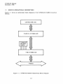
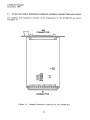
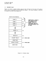
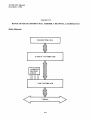
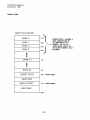
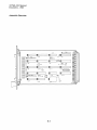
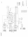
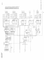
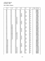
 XVME-202
3U PAMUX Module
USER’S MANUAL
ACROMAG INCORPORATED
30765 South Wixom Road
P.O. BOX 437
Wixom, MI 48393-7037 U.S.A.
Tel: (248) 295-0885
Fax: (248) 624-9234
Email: [email protected]
Copyright 2012, Acromag, Inc., Printed in the USA.
Data and specifications are subject to change without notice.
8500-966B XVME-202 Manual
December, 1986
Chapter 1
INTRODUCTION
1.1 OVERVIEW
The XVME-202 PAMUX Interface Module is a single high, VMEbus compatible board
which allows a VMEbus master to communicate with a PAMUX I/O subsystem. The
specific features of the XVME-202 Interface Module are listed below:
Directly compatible with PAMUX I/O system.
16 PAMUX units can be addressed from one module providing up to
5 12 I/O points.
Termination resistors provided on board.
Connection is made via a 50 conductor ribbon cable.
Cable length can be up to 500 feet.
The XVME-202 occupies a 1K block of the VMEbus short I/O Address Space. The
module address decode logic allows the user to select (via 6 jumpers) any one of 64
of the 1K boundaries in the short I/O Address Space to be used as the module base
address. The module’s Internal Registers are accessible at specific addresses offset
from the selected module base address.
1.2
MANUAL
STRUCTURE
This manual consists of three chapters which divide the various aspects of module
specification and operation into three distinct areas. The three chapters develop
these aspects in the following progression:
Chapter One - A general description of the XVME-202 PAMUX Interface
Module, including complete functional and environmental specifications, VME bus
compliance information, and a block diagram.
Chapter Two - Module installation information covering module specific system
requirements, jumpers, and connector pinouts.
Chapter Three - Details covering functional addressing, and programming
considerations.
The Appendices are designed to provide additional information in terms of the
backplane signal/pin descriptions, a block diagram and assembly drawing, and module
schematics.
1-l
XVME-202 Manual
December, 1986
1.4
MODULE
SPECIFICATIONS
The following is a list of the operational and environmental specifications for the
XVME-202 PAMUX Interface Module.
Power Requirements .
+5V, 1.6A typ., 1.8 A max
Board Dimensions
150 x 116.7 mm
Temperature
Operating
.
Non-Operating
Humidity
.
.
.
0 to 65 degrees C
32 to 149 degrees F
.
-40 to 85 degrees C
-40 to 158 degrees F
.
5 to 95% RH non-condensing
(Extremely low humidity may
require protection against
static discharge.)
Altitude
Operating . .
Non-Operating .
Vibration
Operating
.
Sea-level to 10,000 ft. (3048m)
Sea-level to 50,000 ft. (15240m)
.
5 to 2000 Hz
0.0 15” peak-to-peak displacement
2.5 g peak acceleration
.
5 to 2000 Hz
0.030” peak-to-peak displacement
5.0 g peak acceleration
.
.
30 g peak acceleration’
11 msec duration
Non-operating
.
50 g peak acceleration
11 msec duration
Non-Operating
Shock
Operating
Complies with VMEbus Standard
Revision C. 1
A16:D08(0) DTB Slave
Form Factor - SINGLE
Base address jumper-selectable
on 1K boundaries within the
VMEbus short I/O address space
VMEbus Compliance .
I-3
XVME-202 Manual
December, 1986
Compatibility
VMEbus
.
Access
.
.
Time.
.
.
.
.
.
.
Compatible
with OPT0 2 2
PAMUX 4 *(or PAMUX 2 if the
PAMUX unit is configured for
8-bit use)
.
.
.
DSO ASSERTED TO DTACK ASSERTED (READ)
DSO ASSERTED TO DTACK ASSERTED (WRITE)
DSO NEGATED TO DTACK NEGATED
.
.
1-4
Typical
Maximum
2500nS
500nS
65nS
2700nS
600nS
IOOnS
XVME-202 Manual
December, 1986
Chapter 2
INSTALLATION
2.1 INTRODUCTION
This chapter explains how to configure the XVME-202 PAMUX Interface Module
prior to installation in a VMEbus backplane. Included in this chapter is information
on module base address selection jumpers, address modifier jumper, connector
pinouts, and a brief outline of the physical installation procedure.
2.2
SYSTEM
REQUIREMENTS
The XVME-202 PAMUX Interface Module is a single high VMEbus compatible
module. To operate, it must be properly installed in a VMEbus backplane.
The minimum system requirements for the operation of an XVME-202 PAMUX
Interface Module are one of the following:
A)
-
A host processor properly installed on the same backplane.
A properly installed system controller module which provides the
following functions:
-----
Data Transfer Bus Arbiter
System Clock driver
System Reset driver
Bus time-out module
An example of such a controller subsystem is the XYCOM XVME-010 System
Resource Module (SRM).
B)
l
A host processor which incorporates the system controller functions
on-board.
An example of such a processor is the XVME-600 or the XVME-601.
Prior to installing the XVME-202 PAMUX Interface Module, it will be necessary to
configure three jumper options. These options are:
1)
Module base address within the short I/O address space.
2)
Address Modifier codes to which the Module will respond.
3)
Select SYSCLOCK or on-board Oscillator.
2-1
XVME-202 Manual
December, 1986
2.4 XVME-202 MODULE JUMPER LIST
Table 2-1. Module Jumper List
USE
JUMPER
2.4.1
JlA
Selects optional on-board oscillator.
JlB
Selects SYSCLK from VMEbus.
J2
Determines whether the module will respond to supervisory
or non-privileged short I/O VMEbus cycles (refer to section
2.4.2 of this manual).
JAl0-JAI5
Select module base address on any one of the 64 1K boundaries
within the short I/O address space (refer to Section 2.4.1 of
this manual).
Base Address Jumpers
The XVME-202 can be configured to be addressed at any one of the 64 1K
boundaries within the VME Short I/O Address space by using jumpers JAl0 through
JA15 (see Figure 2-1 for the location of the jumpers on the board) as shown in
Table 2-2.
2-3
XVME-202 Manual
December, 1986
Table 2-2. Base Address Jumper Options
JA15
JA14
JA13
JA12
JAll
JAI0
Base Address
IN
IN
IN
IN
IN
IN
IN
IN
IN
IN
IN
IN
IN
IN
IN
IN
IN
IN
IN
IN
IN
IN
IN
IN
IN
IN
IN
IN
IN
IN
IN
IN
OUT
OUT
OUT
OUT
OUT
OUT
OUT
OUT
OUT
OUT
OUT
OUT
OUT
IN
IN
IN
IN
IN
IN.
IN
IN
IN
IN
IN
IN
IN
IN
IN
IN
OUT
OUT
OUT
OUT
OUT
OUT
OUT
OUT
OUT
OUT
OUT
OUT
OUT
OUT
OUT
OUT
IN
IN
IN
IN
IN
IN
IN
IN
IN
IN
IN
IN
IN
IN
IN
IN
IN
IN
IN
IN
IN
OUT
OUT
OUT
OUT
OUT
OUT
OUT
OUT
IN
IN
IN
IN
IN
IN
IN
IN
OUT
OUT
OUT
OUT
OUT
OUT
OUT
OUT
IN
IN
IN
IN
IN
IN
IN
IN
OUT
OUT
OUT
OUT
OUT
IN
IN
IN
IN
OUT
OUT
OUT
OUT
IN
IN
IN
IN
OUT
OUT
OUT
OUT
IN
IN
IN
IN
OUT
OUT
OUT
OUT
IN
IN
IN
IN
OUT
OUT
OUT
OUT
IN
IN
IN
IN
OUT
OUT
OUT
OUT
IN
IN
IN
IN
OUT
IN
IN
OUT
OUT
IN
IN
OUT
OUT
IN
IN
OUT
OUT
IN
IN
OUT
OUT
IN
IN
OUT
OUT
IN
IN
OUT
OUT
IN
IN
OUT
OUT
IN
IN
OUT
OUT
IN
IN
OUT
OUT
IN
IN
OUT
OUT
IN
IN
OUT
OUT
IN
IN
OUT
IN
OUT
IN
OUT
IN
OUT
IN
OUT
IN
OUT
IN
OUT
IN
OUT
IN
OUT
IN
OUT
IN
OUT
IN
OUT
IN
OUT
IN
OUT
IN
OUT
IN
OUT
IN
OUT
IN
OUT
IN
OUT
IN
OUT
IN
OUT
IN
OUT
IN
OOOOH
0400H
OSOOH
OCOOH
1 OOOH
1400H
1800H
ICOOH
2000H
2400H
2800H
2COOH
3000H
3400H
3800H
3COOH
4000H
4400H
4800H
4COOH
5000H
5400H
5800H
5COOH
6000H
6400H
6800H
6COOH
7000H
7400H
7800H
7COOH
8000H
8400H
8800H
8COOH
9000H
9400H
9800H
9COOH
AOOOH
A400H
A800H
ACOOH
BOOOH
2-4
XVME-202 Manual
December, 1986
Table 2-2.
OUT
OUT
OUT
OUT
OUT
OUT
OUT
OUT
OUT
OUT
OUT
OUT
OUT
OUT
OUT
OUT
OUT
OUT
OUT
2.4.2
IN
IN
IN
OUT
OUT
OUT
OUT
OUT
OUT
OUT
OUT
OUT
OUT
OUT
OUT
OUT
OUT
OUT
OUT
Base Address Jumper Options (Cont’d)
OUT
OUT
OUT
IN
IN
IN
IN
IN
IN
IN
IN
OUT
OUT
OUT
OUT
OUT
OUT
OUT
OUT
OUT
OUT
OUT
IN
IN
IN
IN
OUT
OUT
OUT
OUT
IN
IN
IN
IN
OUT
OUT
OUT
OUT
IN
OUT
OUT
IN
IN
OUT
OUT
IN
IN
OUT
OUT
IN
IN
OUT
OUT
IN
IN
OUT
OUT
OUT
IN
OUT
IN
OUT
IN
OUT
IN
OUT
IN
OUT
IN
OUT
IN
OUT
IN
OUT
IN
OUT
B4OOH
BSOOH
BCOOH
COOOH
C400H
C800H
CCOOH
DOOOH
D400H
DSOOH
DCOOH
EOOOH
E400H
E800H
ECOOH
FOOOH
F400H
F800H
FCOOH
Address Modifier Jumper
The XVME-202 has one jumper that determines which Address Modifier Codes it will
respond to. This jumper is labeled as J2 (see Figure 2-1 for the jumper location).
Jumper J2 determines whether the module will respond to supervisory or to nonprivileged short I/O VMEbus
cycles. When jumper J2 is in, the module will respond
to supervisory short I/O bus cycles only. When jumper J2 is out, the module will
respond to both non-privileged and supervisory short I/O bus cycles. Table 2-3
shows the relationship between jumper J2 and the Address Modifiers.
Table 2-3. Addressing Options
Jumper J2
Address Modifier that the XVME-202 Module will
respond to
In
Out
(2DH) Supervisory Only
(2DH) Supervisory or (29H) Non-privileged
2-5
XVME-202 Manual
December, 1986
2.5 JKl Pin Assignments
The XVME-202 interconnects to the PAMUX bus via JKl on the front panel. The
PAMUX bus has 8 data lines, 6 address lines, a read strobe line, a write strobe
line, and a reset line. Table 2-4 shows the standard PAMUX pin out.
NOTE
The JKI connector is directly compatible with the PAMUX
I/O systems, flat cables can be connected directly from
the XVME-202 to the PAMUX system without the need for a
transition interface.
Table 2-4. PAMUX ‘in out
JKl Pin
Signal
1
3
5
7
9
11
13
15
49
A0
Al
NOTE:
2.6
MODULE
, JKl Pin
~ 33
35
A2
’ 37
A3
~ 39
A4
’ 41
A5
43
WRITE STROBE
45
READ STROBE I 47
RESET
Signal
D7
D6
D5
D4
D3
D2
Dl
D0
All even numbered pins on connector JKl are tied to logic
ground.
INSTALLATION
XYCOM VME modules are designed to comply with all physical and electrical
VMEbus backplane specifications. The XVME-202 PAMUX Interface Module is a
single-high, single-wide VMEbus module, and as such, only requires the P1
backplane.
2-6
XVME-202 Manual
December, 1986
CAUTION
Never attempt to install or remove any boards
before turning off the power to the bus, and all
related external power supplies.
Prior to installing a module, you should determine
and verify all relevant jumper configurations, and
all connections to external devices or power supplies.
(Please check the jumper configuration against the
diagrams and lists in this manual.)
To install a board in the cardcage, perform the following steps:
1)
Make certain that the particular cardcage slot which you are going to use
is clear and accessible.
2)
Center the board on the plastic guides in the slot so that the handle on
the front panel is towards the bottom of the cardcage.
3)
Push the card slowly toward the rear of the chassis until the connectors
engage (the card should slide freely in the plastic guides).
4)
Apply straight-f orward pressure to the handle located on the front panel
of the module until the connector is fully engaged and properly seated.
NOTE
It should not be necessary to use excessive pressure
or force to engage the connectors. If the board does
not properly connect with the backplane, remove the
module and inspect all connectors and guide slots for
possible damage or obstructions.
5)
2.7
Once the board is properly seated, it should be secured to the chassis by
tightening the two machine screws at the extreme top and bottom of the
board.
CONNECTING THE PAMUX UNIT
On the PAMUX connector there is a notch indicating where pin 1 is located (refer
to Figure 2-2). On XYCOM’s XVME-202 PAMUX Interface Adapter the ribbon
connector has a similar notch indicating the position of pin 1.
2-7
XVME-202 Manual
December, 1986
To connect a PAMUX (or a string of PAMUXs), plug one end of a flat ribbon cable
into the XVME-202 JKl connector so Pin 1 on the XVME-202 JKl is connected to
Pin 1 of the PAMUX connector (refer to Figure 2-2).
It is possible to connect 16 PAMUX Units in a daisy chain to the XVME-202 (see
Figure 2-3) as long as the total length of the ribbon does not exceed 500 feet.
2.8 OPTIONAL ON-BOARD OSCILLATOR
Jumper Jl is used to select between the VMEbus signal SYSCLK
MHz oscillator. Position JIB selects the VMEbus SYSCLK and is
For systems where SYSCLK is not provided
this position.
backplane, A 16 MHz oscillator, Ul9, can be installed and selecting
will operate with its own clock.
Oscillator
XVME - 202
ADAPTER
PAMUX
type:
or an optional 16
factory shipped in
on the VMEbus
JlA, the module
MXO-55GA-2C-16.0MHz
or equivalent
CTS Knights
.
I
/
PAMUX
1
I
PAMUX
.
PAMUX
1
r
Figure 2-3. PAMUX Daisy Chain
2-9
XVME-202 Manual
December, 1986
2.9
INSTALLING A 6U FRONT PANEL KIT (optional)
XYCOM Model Number XVME-943 is an optional 6U front panel kit designed to
replace the existing 3U front panel on the XVME-600.
The 6U front panel
facilitates the secure installation of single-high modules in those chassis which are
designed to accommodate double-high modules. The following is a step-by-step
procedure for installing the 6U front panel on an XVME-600 Module (refer to figure
2-4 for a graphic depiction of the installation procedure).
1.
Disconnect the module from the bus.
2..
Remove the screw and plastic collar assemblies (labeled #6 and #7) from
the extreme top and bottom of the existing 3U front panel (#ll), and
install the screw assemblies in their corresponding locations on the 6U
front panel.
3.
Slide the module identification plate (labeled #13) from the handle (#9) on
the 3U front panel. By removing the screw/nut found inside the handle,
the entire handle assembly will separate from the 3U front panel.
Remove the counter-sunk screw (#8) to separate the 3U front panel from
the printed circuit board (#12).
4.
Line-up the plastic support brackets on the printed circuit board with the
corresponding holes in the 6U front panel (i.e. the holes at the top and
top-center of the panel). Install the counter-sunk screw (#8) in the hole
near the top center of the 6U panel, securing it to the lower support
bracket on the printed circuit board.
5.
Install the handle assembly (which was taken from the 3U panel) at the
top of the 6U panel, using the screw and nut previously attached inside
the handle. After securing the top handle, slide the module identification
plate in place.
6.
Finally,
install the bottom handle (i.e. the handle that accompanies the
.
kit - labeled #2) using the screw and nut (#3 & #5) provided. Slide the
XYCOM VMEbus I.D. plate (#4) in place on the bottom handle. The
module is now ready to be re-installed in the backplane.
2-10
XVME-202 Manual
December, 1986
Chapter 3
MODULE PROGRAMMING
3.1
INTRODUCTION
This chapter will briefly examine the addressing, and initialization procedures and
constraints required when programming the XVME-202 PAMUX Interface Adapter.
3.2 MODULE ADDRESSING
The XVME-202 is an odd byte only slave, and as such, the module will not respond
to even, single-byte accesses.
However, word accesses may be used, with the
understanding that only the odd byte of the word is used to exchange PAMUX data.
The PAMUX data bus is only 8-bits wide, while the PAMUX unit contains 32 points
of I/O.
To be able to access all 32 points, the PAMUX is composed of 4
consecutive banks of 8 I/O channels (refer to Figure 3-l). Refer to the OPTO 22,
PAMUX 4 32 Channel Data Acquisition/Control System manual for information about
how to assign each PAMUX unit a base address. With 16 PAMUX units connected
to the XVME-202, there will be a block of 64 consecutive 8-bit banks that could be
accessed.
3-1
XVME-202 Manual
December, 1986
3.4
RESET
The PAMUX unit has a Reset line that is used for turning off the relays on all
PAMUX units on the bus. On power-up and in response to SYSRESET, the Reset is
asserted on the XVME-202 which causes the attached PAMUX units to be reset.
The user must deactivate the Reset line by performing a write operation to Base
address + C1H. To activate RESET, perform a write operation to Base Address +
81H.
The XVME-202 uses a active low Reset line. Refer to the PAMUX manual for
information on how to select the correct Reset polarity on the PAMUX unit.
3.5 READ/WRITE
To read a bank it is necessary to indicate the base address (for example, 1000H
plus the bank address. Using the Memory Map (Figure 3-2), if the user needed to
read bank 12, they would simply perform a read operation from location 1019H.
This is also true if the user wished to write to bank 12.
When the user is writing to a relay bank that has input and output modules, the
user MUST make sure that zeros are written to the input module positions. If the
user write’s a 1 to an input module by mistake, the module will read back as being
active even if it is inactive.
,
3.6 VMEbus ACCESS TIME
The PAMUX unit requires a read/write strobe pulse width of 2 uSec.
It then
requires another 2 uSec before another read/write strobe can be generated.
Therefore, on a read cycle, DTACK will be asserted 2.5 uSec. after the start of the
cycle, but the XVME-202 cannot be accessed for another 1.5 uSec. after DTACK.
During a write cycle, the data is latched on the module and DTACK will be
generated within 500 nSec. If an attempt is made to access the XVME-202 during
this time, DTACK will be delayed further. Table 3-1 shows the DTACK access time.
Table 3-1. DTACK Access Time
Description
DSO ASSERTED TO DTACK ASSERTED (READ)
DSO ASSERTED TO DTACK ASSERTED (WRITE)
DSO NEGATED TO DTACK NEGATED
3-4
Typical
2500nS
500nS
65nS
Maximum ,
2700nS
600nS
1OOnS
XVME-202 Manual
December, 1986
Appendix A
VMEbus CONNECTOR/PIN DESCRIPTION
Table A-l. Pl - VMEbus Signal Identification
Signal
Mnemonic
Connector
and
Pin Number
ACFAIL*
lB:3
Signal Name and Description
AC FAILURE: Open-collectors driven signal which
indicates that the AC input to the power supply is no
longer being provided, or that the required input
voltage levels are not being met.
IACKIN*
lA:21
INTERRUPT ACKNOWLEDGE IN: Totem-pole driven
signal. IACKIN* and IACKOUT* signals form a daisychained acknowledge. The IACKIN* signal indicates to
the VME board that an acknowledge cycle is in
progress.
IACKOUT*
1A:22
INTERRUPT ACKNOWLEDGE OUT: Totem-pole driven
signal. IACKIN* and IACKOUT* signals form a daisychained acknowledge. The IACKOUT* signal indicates
to the next board that an acknowledge cycle is in
progress.
AM0-AM5
1A:23
lB:16,17,
18,19
lC:14
ADDRESS MODIFIER (bits 0-5): Three-state driven
lines that provide additional information about the
address bus, such as: size, cycle type, and/or DTB
master identification.
AS*
lA:l8
ADDRESS STROBE: Three-state driven signal that
indicates a valid address is on the address bus.
A-l
XVME-202 Manual
December, 1986
Table A-1. VMEbus Signal Identification (cont’d)
Signal
Mnemonic
Connector
and
Pin Number
A0l-A23
1A:24-30
lC:15-30
ADDRESS BUS (bits l-23): Three-state driven address
lines that specify a memory address.
A24-A31
2B:4-11
ADDRESS BUS (bits 24-31): Three-state driven bus
expansion address lines.
BBSY*
1B:l
BUS BUSY: Open-collector driven signal generated by
the current DTB master to indicate that it is using the
bus.
BCLR*
lB:2
BUS CLEAR: Totem-pole driven signal generated by the
bus arbitrator to request release by the DTB master if
a higher level is requesting the bus.
BERR*
1C:ll
BUS ERROR: Open-collector driven signal generated by
a slave. It indicates that an unrecoverable error has
occurred and the bus cycle must be aborted.
BG0IN*BG3IN*
1B:4,6,
8,l0
BUS GRANT (0-3) IN: Totem-pole driven signals
generated by the Arbiter or Requesters. Bus Grant In
and Out signals form a daisy-chained bus grant. The
Bus Grant In signal indicates to this board that it may
become the next bus master.
BG0OUT*BG3OUT*
1B:5,7,
9,ll
BUS GRANT (0-3) OUT: Totem-pole driven signals
generated by Requesters. These signals indicate that a
DTB master in the daisy-chain requires access to the
bus.
Signal Name and Description
A-2
XVME-202 Manual
December, 1986
Table A-1. VMEbus Signal Identification (cont’d)
Signal
Mnemonic
Connector
and
Pin Number
BR0*-BR3*
lB:12-15
BUS REQUEST (0-3): Open-collector driven signals
generated by Requesters. These signals indicate that a
DTB ‘master in the daisy-chain requires access to the
bus.
DSO*
lA:13
DATA STROBE 0: Three-state driven signal that
indicates during byte and word transfers that a data
transfer will occur on data buss lines (D00-D07).
DSl*
lA:12
DATA STROBE 1: Three-state driven signal that
indicates during byte and word transfers that a data
transfer will occur on data bus lines (D08-D15).
DTACK*
lA:16
DATA TRANSFER ACKNOWLEDGE: Open-collector
driven signal generated by a DTB slave. The falling
edge of this signal indicates that valid data is available
on the data bus during a read cycle, or that data has
been accepted from the data bus during a write cycle.
D00-D15
lA:l-8
lC:l-8
DATA BUS (bits 0-15): Three-state driven, bidirectional data lines that provide a data path between
the DTB master and slave.
GND
lA:9,11,
15,17,19,
1B:20,23,
lC:9
2B:2,12,
22,31
GROUND
Signal Name and Description
A-3
XVME-202 Manual
December, 1986
Table A-l. VMEbus Signal Identification (cont’d)
Signal
Mnemonic
Connector
and
Pin Number
IACK*
1 A:20
INTERRUPT ACKNOWLEDGE: Open-collector or threestate driven signal from any master processing an
interrupt request. It is routed via the backplane to
slot 1, where it is looped-back to become slot 1
IACKIN* in order to start the interrupt acknowledge
daisy-chain.
IRQl*IRQ7*
1B:24-30
INTERRUPT REQUEST (1-7): Open-collector driven
signals, generated by an interrupter, which carry
prioritized interrupt requests.
Level seven is the
highest priority.
LWORD*
lC:13
LONGWORD: Three-state driven signal
the current transfer is a 32-bit transfer.
(RESERVED)
2B:3
RESERVED: Signal line reserved for future VMEbus
enhancements. This line must not be used.
SERCLK
lB:21
A reserved signal which will be used as the clock for a
serial communication bus protocol which is still being
finalized.
SERDAT
1 B:22
A reseved signal which will be used as the transmission
line for serial communication bus messages.
SYSCLK
lA:10
SYSTEM CLOCK: A constant 16-MHz clock signal that
is independent of processor speed or timing. It is used
for general system timing use.
Signal Name and Description
A-4
indicates
that
XVME-202 Manual
December, 1986
Table A-l. VMEbus Signal Identification (cont’d)
Signal
Mnemonic
Connector
and
Pin Number
SYSFAIL*
1C:l0
SYSTEM FAIL: Open-collector driven signal that
indicates that a failure has occurred in the system. It
may be generated by any module on the VMEbus.
SYSRESET*
lC:12
SYSTEM RESET: Open-collector driven signal which,
when low, will cause the system to be reset.
WRITE*
lA:14
WRITE: Three-state driven signal that specifies the
data transfer cycle in progress to be either read or
written. A high level indicates a read operation, a low
level indicates a write operation.
+5V STDBY
lB:31
+5 VDC STANDBY: This line supplies +5 VDC to devices
requiring battery backup.
+5v
lA:32
lB:32
1C:32
2B:1,13,32
+5 VDC POWER: Used by system logic circuits.
+12v
lC:31
+12 VDC POWER: Used by system logic circuits.
-12v
lA:31
-12 VDC POWER: Used by system logic circuits.
Signal Name and Description
A-5
Manual
December, 1986
XVME-202
BACKPLANE CONNECTOR Pl
The following table lists the Pl pin assignments by pin number order.
connector consists of three rows of pins labeled rows A, B, and C.)
Table A-2. Pl Pin Assignments
Pin
Number
Row A
Signal
Mnemonic
Row B
Signal
Mnemonic
Row C
Signal
Mnemonic
1
D00
2
3
DO1
DO8
DO9
DO2
BBSY *
BCLR*
ACFAIL*
4
DO3
BGOIN*
5
6
7
DO4
DO5
8
9
10
11
12
13
14
15
16
17
18
19
20
21
22
23
24
25
26
27
28
29
DO6
DO7
GND
SYSCLK
BG3IN*
GND
DSI*
BG3OUT*
BRO*
BRl*
BERR*
SYSRESET*
GND
AS *
GND
BR2*
BR3*
AM0
AM1
AM2
AM3
LWORD*
AM5
A23
A22
A21
A20
A19
IACK*
GND
Al8
SERCLK( 1)
A17
SERDAT( 1)
Al6
DSO*
WRITE*
GND
DTACK*
IACKIN*
IACKOUT*
AM4
A07
A06
A05
A04
A03
31
A02
A01
-12v
32
+5v
30
BGOOUT*
BGlIN*
BGlOUT*
BG2IN*
BG20UT*
Dl0
Dll
D12
D13
D14
D15
GND
SYSFAIL*
GND
A15
IRQ7*
A14
IRQ6*
IRQ5*
A13
A12
IRQ4*
All
A10
IRQ3*
IRQ2*
IRQl*
+5v STDBY
+5v
A-6
A09
A08
+12v
+5v
(The