1
GR712RC
5
Fault Tolerant Memory Controller
5.1
Overview
The combined 8/32-bit memory controller provides a bridge between external memory and the AHB
bus. The memory controller can handle four types of devices: PROM, asynchronous static RAM
(SRAM), synchronous dynamic RAM (SDRAM) and memory mapped I/O devices (IO). The PROM,
SRAM and SDRAM areas can be EDAC-protected using a (39,7) BCH code. The BCH code provides
single-error correction and double-error detection for each 32-bit memory word.
The SDRAM area can optionally also be protected using Reed-Solomon coding. In this case a 16-bit
checksum is used for each 32-bit word, and any two adjacent 4-bit (nibble) errors can be corrected.
The memory controller is configured through three configuration registers accessible via an APB bus
interface. The external data bus can be configured in 8-, or 32-bit mode, depending on application
requirements. The controller decodes three address spaces on the AHB bus (PROM, IO, and SRAM/
SDRAM). The IO area is marked as non-cacheable in the core’s AMBA plug’n’play information
record.
External chip-selects are provided for two PROM banks, one IO bank, two SRAM banks and two
SDRAM banks. Note that when the EDAC is enabled in 8-bit bus mode, only the first PROM and
SRAM banks can be used under certain circumstances, see section 5.10 for details.
The maximum PROM capacity supported is 32 MiB + 25% for EDAC checksum over 2 banks.
The maximum SRAM capacity supported is 32 MiB + 25% for EDAC checksum over 2 banks.
The maximum SDRAM capacity supported is 1 GiB + 25% or 50% for EDAC checksum over 2
banks when not using SRAM. When also using SRAM the maximum amount of supported SDRAM
is 512 MiB + 25% or 50% for EDAC checksum over 1 or 2 banks.
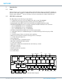
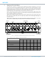
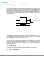
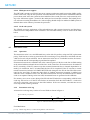
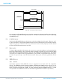
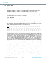
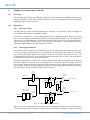
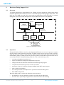
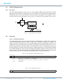
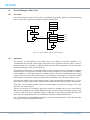
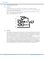
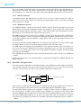
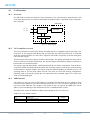
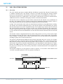
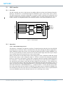
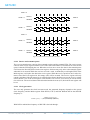
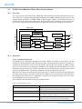
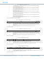
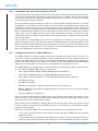
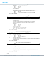
Figure 15 below shows how the connection to the different device types is made.
APB
A
AHB
APB
ROMSN[1 :0]
OEN
WRITEN
CS
OE
WE
PROM
IOSN
CS
OE
WE
I/O
RAMSN[1:0]
RAMOEN
RAMWEN
CS
OE
WE
SRAM
SDCSN[1:0]
SDRASN
SDCASN
SDWEN
SDDQM[3:0]
CSN
RAS
CAS
WE
DQM
FTMCTRL
AHB
SDRAM
D
CB
A
D
CB
A
D
A
D
CB
A
D
CB
ADDRESS[23:0]
DATA[31:0]
CB[15:0]
Figure 15. FTMCTRL connected to different types of memory devices
GR712RC-UM, Nov 2015, Version 2.6
52
www.combham.com/gaisler