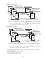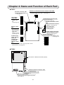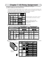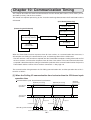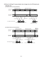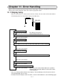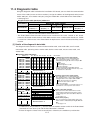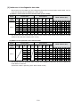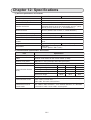
1
Version 2.0
Produced in August, 2006
Sharp Programmable Controller
Board PC
J-board
Model name
DeviceNet Master Board
User's Manual
Z-337J/338J
Thank you for purchasing this device net master board Z-337J/338J for sharp PLC J-board Z300/500.
This manual describes the specifications, usage etc. of the Z-337J/338J.
Please familiarize yourself with the board by reading this user’s manual thoroughly.
In addition to this manual, the following manuals are available for your further study.
J-board Z300 series
CPU board
Z-311J/312J User’s manual • Hardware version
(JW20H Programming manual • Ladder instruction version)
J-board Z500 series
CPU board
Z-511J User’s manual • Hardware version
Z-512J User’s manual • Hardware version
(JW30H Programming manual • Ladder instruction version)
Note
- Should you have any questions or inquires, please feel free to contact one of our dealers, or our
service department.
- Copying this manual in part or in total is prohibited.
- The contents of this manual may be changed without notice.
Technical Information No. 04S0033 Attached sheet 1
Make sure to read this insert before using this module
The Z-337J/338J communicates with slave stations that are registered on a scan list it creates. If a slave
station is physically disconnected from the communication line, the Z-337J/338J will not receive a
response from the slave station and a communication error will occur. In order not to cause a system
error, if a slave station is temporarily disconnected and reconnected, a new connection table will be
constructed in the module versions described below.
Note: Please note that the master board will not try to communicate with a slave station whose
corresponding entry is turned ON (disconnected) in the connection table.
Diagnostic table
Register D7 D6 D5 D4 D3 D2 D1 D0
39000
39001
39002
39003
39004
39005
39006
39007
39010
39011
39012
39013
39014
39015
39016
39017
39020
39021
39022
39023
39024
39025
39026
39027
39030
39031
39032
39033
39034
39035
39036
39037
39040
39041
39042
39043
39044
39045
39046
39047
39050
If the top address of the diagnostic table is 39000, the
connection table area will be from 39030 to 39037.
Communication
monitor table (8 bytes)
Error node table (8 bytes)
Scan list table (8 bytes)
7
15
23
31
39
47
55
63
6
14
22
30
38
46
54
62
5
13
21
29
37
45
53
61
4 3 2 1
12 11 10 9
20 19 18 17
28 27 26 25
36 35 34 33
44 43 42 41
52 51 50 49
60 59 58 57
0
8
16
24
32
40
48
56
Connection table area
ON: Disconnected (does not communicate)
OFF: Connected (communicates)
Operating status monitor
table (8 bytes)
[1] The applicable program version number for the connection table and the compatible module
models are as follows.
v4.1 or later
JW20DN2
v2.7 or later
JW32CV3, JW32CUM1, JW32CUM2, Z337J/Z338J
[2] The LEDs and communication status will be as follows when a module is shown as
disconnected in the connection table.
Ex.: A system with a master board (station number 0) and two slave stations (station numbers 1 and
2).
(1) When the D1 bit in 39030 is ON (Slave station 1 is disconnected)
LED
Z-337J/338J
Slave station Slave station
(station No. 0) (station No. 1) (station No. 2)
MS
Lit green
Lit green
Lit green
NS
Lit green
Blinks green
Lit green
S0 to S7
OFF
-
-
Communication status
Only one slave station (station No. 1) is
disconnected and the NS LED will blink
green. The master board will continue
communication with the other slave
station (station No. 2)
Technical Information No. 04S0033 Attached sheet 2
(2) When the D1 and D2 bits in 39030 are ON (Slave stations 1 and 2 are disconnected)
Z-337J/338J
Slave station Slave station
(station No. 0) (station No. 1) (station No. 2)
LED
MS
Lit green
Lit green
Lit green
NS
Blinks green
Blinks green
Blinks green
S0 to S7
OFF
-
-
Communication status
Only one slave station (station No. 1) is
disconnected and the NS LED will blink
green. The master board will continue
communication with the other slave
station (station No. 2).
[3] Recommending program
If you will not be using the connection function, we recommend that you insert the following program
at the end of user program, in order not to disconnect any slave module mistakenly from the user
program.
* When the top address of the diagnostic table is 39000.
0
000001
1
000002
2
000007
F-047
ONLS
007366
F-071
CONS
039030
0
Normally
OFF
039037
0
F-048
ONLR
3
000010
F-040
END
Lighting conditions and meanings of the MS and NS LEDs on the JW-20DN2, version 4.1 or
later, and the JW32CV3, JW32CUM1, JW32CUM2, Z337J/Z338J, version 2.7 or later.
Lamp name Color
Status
ON
In master mode
- The network is normal.
Note: Even if some slave stations are disconnected, as
On-line /
long as one slave station can communicate, this lamp
communication
will be lit.
connection
complete
In slave mode
- The network is normal.
(Normal communication established with a master board.)
Green
Blinking
NS
(Network
status)
Description
On-line / no
communication
In master mode
- Although the network is normal, communication has not
been established.
- Slave stations are disconnected.
(By turning ON (disconnect) the connection table, there are
no slave stations that the master can communicate with.)
In slave mode
- Although the network is normal, communication has not
been established.
- The Z-337J/338J is disconnected from the master board.
ON
Red
Blinking
-
OFF
Same for master and slave mode
- Communication error (the Z-337J/338J detected an error or
Communication
there is unstable communication on the network.)
error 1
- A node address is used twice.
- A busoff error was detected.
Communication
error 2
In master mode
- One or more slave stations have a communication error.
In slave mode
- The Z-337J/338J has a communication error.
Off-line / Power Same for master and slave mode
OFF
- There is no node other than the Z-337J/338J.
Safety Precautions
Read this user's manual and attached documents carefully before installation, operation, maintenance and
checking in order to use this board correctly. Understand all of this board's knowledge, safety information,
and cautions before starting to use. In this user's manual, safety precautions are ranked into "Danger" and
"Caution" as follows.
Danger
: Wrong handling may possibly lead to death or heavy injury.
Caution
: Wrong handling may possibly lead to medium or light injury or loss on properties.
Even in the case of
Caution , a serious result may be experienced depending on the
circumstances. Anyway, important points are mentioned. Be sure to observe them strictly.
The picture signs of prohibit and compel are explained below.
: It means a don’t. For example, prohibition of disassembly is indicated as (
: It means a must. For example, obligation of grounding is indicated as (
).
).
1) Installation
Caution
• Use in the environments specified in the catalog and user's manual.
Electric shock, fire or malfunction may be caused when used in the environments of high
temperature, high humidity, dusty or corrosive atmosphere, vibration or impact.
• Install according to the instruction manual and user's manual.
Wrong installation may cause a drop, trouble or malfunction.
• Never admit wire chips or foreign matters.
Or fire, trouble or malfunction may be caused.
2) Wiring
Compel
• Be sure to ground.
Unless grounded, electric shock or malfunction may be caused.
Caution
• Wiring should be done by a qualified electrician.
Wrong wiring may lead to fire, trouble or electric shock.
3) Use
Danger
• Never touch the terminals while electric power is charged.
Otherwise, you may have an electric shock.
• Assemble an emergency stop circuit and interlock circuit outside of the J-board and integrate
the J-board's halt output. Otherwise a machine breakdown or accident may be caused by the
trouble of the programmable controller.
Caution
• Manipulation for program change, forced output, RUN or STOP during operation should be
done with particular care by confirming safety. Mis-operation may lead to a machine trouble or
accident.
• Follow the power input order specified. Otherwise, the J-board malfunctions and damages
machines or cause an accident.
4) Maintenance
Prohibit
• Don’t disassemble or modify.
Or fire, trouble or malfunction may be caused.
Caution
• Make sure to turn OFF the power before removing / installing the board, installing the
connectors, or changing the switch settings.
Table of Index
Chapter 1: Outline ...................................................................................................... 1-1
Chapter 2: Handling Precautions....................................................................... 2-1 to 2
Chapter 3: System Configuration ...................................................................... 3-1 to 9
3-1 Number of board install into a J-board 3-2
(1) When CPU board is Z-311J/312J 3-2
(2) When CPU board is Z-511J 3-3
(3) When CPU board is Z-512 3-3
3-2 Network configuration of DeviceNet 3-4
[1] Network names and functions 3-5
[2] Connection method 3-6
(1) T branch method 3-6
(2) Multi-drop method 3-6
[3] Cable length 3-7
(1) Maximum network length 3-7
(2) Maximum branch line length 3-7
(3) Communication speed and distance 3-7
[4] Power supply 3-8
[5] Communication related devices 3-9
(1) Cable 3-9
(2) T branch tap 3-9
(3) Power tap 3-9
(4) Communication connector 3-9
(5) Terminating resistance 3-9
(6) Communication power supply 3-9
Chapter 4: Name and Function of Each Part .................................................... 4-1 to 7
(1) Indicators (DeviceNet): Z-337J/338J 4-2
(2) Module No. switch SW3: Z-337J/338J 4-3
(3) Node address switch SW3: Z-337J/338J 4-4
(4) Scan switch SW7: Z-337J/338J 4-4
(5) Number of communication boards switch SWA: Z-337J/338J 4-4
(6) Terminating resistanc switch SW6: Z-337J/338J 4-4
(7) Function switch SW4: Z-337J/338J 4-5
(8) Communication speed, operation mode, communication monitor time switch SW5: Z337J/338J 4-6
(9) External connetor CN3: Z-338J only 4-7
(10) Output proteciton fuse: Z-338 only 4-7
(11) Indicators (input/output): Z-338J only 4-7
Chapter 5: Assembly and Installation Methods ............................................... 5-1 to 3
5-1 Assembly 5-1
5-2 Installation 5-3
Chapter 6: Connection (Wiring) Methods ......................................................... 6-1 to 5
6-1 Connection to the DeviceNet: Z-337J/338J 6-1
[1] Processig of communication cable 6-1
[2] Connection of communication connectors 6-3
6-2 Connection to input/output equipment: Z-338J only 6-4
Chapter 7: I/O Relay Assignment ....................................................................... 7-1 to 3
[1] When installed on Z-311J/312J, Z-512J 7-1
(1) When one communication board (Z-337J or Z-338J) is used 7-1
(2) When two communication boards (Z-337J or Z-338J) are used 7-1
[2] When installed on Z-511J 7-2
(1) When one communication board (Z-337J or Z-338J) is used 7-2
(2) When two communication boards (Z-337J or Z-338J) are used 7-3
Chapter 8: Polling I/O Function .......................................................................... 8-1 to 9
8-1 Input/output data table allocation 8-2
[1] Address order allocation 8-2
[2] Even number allocation 8-4
[3] Allocation in the order in which vacant nodes are occupied 8-6
8-2 Editing the scan list 8-8
[1] Editing procedure 8-8
[2] Scan list table 8-9
Chapter 9: Explicit Message Function .............................................................. 9-1 to 8
[1] Details of the Explicit message data table (requests) 9-1
[2] Details of the Explicit message data table (responses) 9-2
[3] Parameter addresses for the Explicit message table (requests, responses) 9-3
[4] Example 9-4
Chapter 10: Communication Timing .................................................................. 9-1 to 2
[1] When the Polling I/O communication time is shorter than the CPU board cycle operation
time 10-1
[2] When the Polling I/O communication time is longer than the CPU board cycle operation time
10-2
(1) Communication cycle: Asynchronous 10-2
(2) Communication cycle: Synchronous 10-2
Chapter 11: Error Handling .............................................................................. 11-1 to 9
11-1 Display lamp 11-1
[1] Error code 11-1
(1) Error code display 11-1
(2) Error details 11-2
[2] Display of node addresses 11-4
11-2 Diagnostic table 11-5
[1] Details of the diagnositc data table 11-5
[2] Address in the diagnostic data table 11-7
(1) Address of the communication monitor table (master mode) 11-6
(2) Address of the operation status monitor table 11-6
(3) Device statsu table address 11-7
(4) Master status address 11-9
11-3 Slave status when the J-board has stopped operation 11-9
Chapter 12: Specifications ............................................................................... 12-1 to 2
(1) General specifications: Z-337J/338J 12-1
(2) Communication specifications: Z-337J/338J 12-1
(3) Input/output specifications: Z-338J only 12-2
Chapter 1: Outline
The DeviceNet master board, Z-337J/338J is a master board for the J/board Z300/500 series
programmable controllers, and it is used in a DeviceNet (an open network). Installing this board on a Jboard, and connecting various DeviceNet slave devices allows you to construct an optimum system with
decentralized control. In addition, the Z-338J is equipped with 32 points I/O (16 points input and 16 points
output).
De facto standard network
By employing the DeviceNet standards, which have a major share of the market in North America, your
product will have an advantage in that it can be used in oversea's markets, and can share facilities both
in Japan and overseas.
Wire savings by using proprietary cables
One single exclusive cable can be used to connect between nodes (master and slaves). It can also be
branched using a "T" branch tap.
Up to 63 slave stations can be connected
A maximum of 63 slave stations can be connected to one Z-337J/338J master board. (Maximum
number of I/O points: 4096)
Simple operation using a scan list editing function
In addition, the Z-337J/338J is equipped with a Polling I/O function and Explicit message function as a
part of the DeviceNet specifications.
32 I/O points installed (Z-338J only)
The Z-338J has 16 24 VDC input and 16 NPN transistor output points, saving a lot of space.
DeviceNet is a trademark of the ODVA (Open DeviceNet Vendor Association).
1-1
Chapter 2: Handling Precautions
Follow the precautions below when using the Z-337J/338J.
(1) Precautions for installation
Never install the board in the following locations.
· Where proximate to any heat generating object.
· Where temperature rapidly changes and gives dew condensation.
· Where there is corrosive or flammable gas.
· Where it directly receives vibration or shocks.
· Where exposed to dust, iron powder, or salty atmosphere.
(In conditions where the printed circuit boards may be directly affected by these causes, make sure to
provide an appropriate external case to cover the J-board.)
· Where it is proximate to high voltage equipment, driving power tools, large open/close surge generating devices, and their wirings.
(2) Precautions at use
· In order to prevent personal injury or damage to equipment, construct an external emergency stop
circuit and connect it to the halt output on the J-board.
· As J-board is board structure and it’s electronic parts are exposed, be careful when handling.
1) Before you touch the board directly, be sure to eliminate static electricity in your body.
2) Do not touch directly with dirty hands such as stacked oil etc.
3) Do not put the board alone directly on conductive objects such as metallic boards.
(Once the J-board is installed on a motherboard, if it contacts a conductive object the battery on
the motherboard may be short circuited and the back up memory may be damaged.)
4) Be careful not to apply excessive force to each switch, connector, terminal block of the J-board.
· Make sure to turn OFF the power before connecting the board, installing connector, changing a
switch setting.
(3) Grounding
· The FG terminal (CPU board terminal block) on the J-board must not share a ground point with high
voltage applications. Set up an independent, class 3 ground for the FG terminal.
· The hexagonal stand-offs on each board, that are used to install the J-board, are also used to
connect the board to ground (FG). Tighten them securely.
(4) Precautions for wiring
Do not run the communication lines parallel to or near to power lines or high voltage lines. Do not
arrange wiring so that sources of electrical noise (driver lines, high voltage lines, or I/O lines) come
close to the PC board on the J-board.
2-1
(5) Installation
Use bracket A or B (sold separately) to install the J-board in any of the following 4 positions.
Recommending installation positions
1
2
3
When fixing bracket A (Z-341J) is used
4
When fixing bracket B (Z-342J) is used
If you do not use bracket A or B to install the J-board, make sure it is very secure. Also, install the Jboard with as much ventilation as possible.
If the J-board is installed horizontally, as shown in the figure below, it will not be well ventilated. Make
sure the installation allows enough space above the board so that the surrounding temperature does
not rise above 55˚C.
Not good ventilation
(6) Output protection fuse: Z-338J only
When the output protection fuse on the Z-338J is blown, after resolving the problem such as a short
circuit in a load, replace the fuse. The output protection fuse on the Z-338J is there to protect the
internal circuits from damage due to overcurrent or shorted loads. It is not there to protect the output
elements.
2-2
Chapter 3: System Configuration
J-board (Z300/500 series)
* Number of boards to install into a J-board
=> See page 3-2 and 3-3.
CPU board
Z-311J
Z-312J
Z-511J
Z-512J
*
Z-337J
Z-338J
SWA
SWA
SW4
5
6
7
8
SW7 ON← SW6
3
5
6
7
8
1
2
3
4
5
SW5
1
2
DeviceNet network
=> See page
3-4 to 3-9
6
7
8
SW7 ON← SW8
7
8
4
1
SW3
6
SW4
3
4
5
2
1
1
2
2
3
4
O
F
F
↓
ON
2
ON
1
O
F
F
↓
DeviceNet network
=> See page
3-4 to 3-9
SW3
3
SW6
2
4
SW5
3
SW3
1
1
2
Input/output equipment
=> See section 6-2.
C0
C1
C2
C3
C4
C5
C6
C7
D0
D1
D2
D3
D4
D5
D6
D7
A0
A1
A2
A3
A4
A5
A6
A7
B0
B1
B2
B3
B4
B5
B6
B7
4
332 points I/O
24 VDC input: 16 points
NPN transistor output: 16 points
3-1
3-1 Number of board install into a J-board
The Z-337J/338J is a communication board of the J-board. The maximum number of boards to install
into a J-board are total number of boards including the communication boards.
Number of Z-337J/338J boards to install
J-board CUP board
(including other communication boards)
Maximum 2 boards
Z-311J
Z300
- When the total of 5 V power consumption current of boards
series
Z-312J
installed exceed 800 mA, the number of boards is restricted.
Maximum 2 boards
- 5 V power supply (outside connection) is needed a capacity of
Z-511J
total 5 V power consumption current of each board installed
Z500
(max. 2.7 A).
series
Maximum 2 boards
- When the total of 5 V power consumption current of boards
Z-512J
installed exceed 1.8 A, the number of boards is restricted.
Types of communication boards
Z-331J *
Specifications
Data link or computer link, satellite I/O link master station
Z-332J
Z-333J
Z-334J
Data link or computer link
Satellite I/O link master station
ME-NET board (with branch line extension function)
Z-335J
Z-336J
Satellite net board
FL-net board
Z-337J
Z-338J
Devicenet master board
DeviceNet master board (with 32 points I/O)
Model name
*Manufacture after ordered
(1) When CPU board is Z-311J/312J
Stacked connection
- Connectable up to 4 boards of I/O, communication,
and special I/O boards. (Up to 2 communication boards)
CPU board
Z-311J
Z-312J
Z-337J
Z-338J
SWA
SWA
1
4
SW3
5
SW4
3
3
4
2
1
1
2
2
5
O
F
F
↓
ON
2
ON
1
O
F
F
↓
6
7
6
8
7
8
1
2
3
6
7
8
SW7 ON← SW6
5
SW4
4
5
SW7 ON← SW8
4
2
3
SW5
1
6
7
8
1
SW3
SW3
4
SW5
3
3
SW6
2
1
2
C0
C1
C2
C3
C4
C5
C6
C7
D0
D1
D2
D3
D4
D5
D6
D7
A0
A1
A2
A3
A4
A5
A6
A7
B0
B1
B2
B3
B4
B5
B6
B7
4
3-2
Maximum 2 boards of Z-337J/338J
can be installed (including other
communication boards).
(2) When CPU board is Z-511J
Stacking connection (Note)
- Maximum 4 boards of I/O,
Horizontal installation
communication, and special
I/O boards can be connected
Stacking connection (note)
(up to 2 communication boards).
- Maximum 4 boards of I/O
and special I/O boards
can be connected
(communication boards
cannot be connected).
Extension cable
CPU board
(Z-511J)
Z-337J
Z-338J
- JW-203EC (30 cm)
- JW-207EC (70 cm)
*1
Z-356J
Note: With a system using the Z-511J, total number of
boards installed including horizontal installation is 7.
The Z-337J/338J can be installed with maximum 2 boards (including other communication boards).
*1. When to install horizontally, the Z-511J (CUP board) and Z-356J (high-speed counter
board) shall be connected using an expansion cable.
(3) When CPU board is Z-512J
Stacking connection
- Maximum 4 boards of I/O,
Horizontal installation
communication, and special
I/O boards can be connected
Stacking connection
(up to 2 communication boards).
- Maximum 4 boards of I/O
and special I/O boards
can be connected
(communication boards
cannot be connected).
Extension cable
CPU board
(Z-512J)
- JW-203EC (30 cm)
- JW-207EC (70 cm)
*2
Z-356J
- With a system using the Z-512J, total number of
boards including horizontal installation is 8.
Z-337J
Z-338J
The Z-337J/338J can be installed maximum 2 boards (including other communication boards).
*2. When to install horizontally, the Z-512J (CUP board) and the Z-356J (high-speed counter
board) shall be connected using an expansion cable.
As for the details of number of boards and modules connectable to the CPU board, see the following
manuals for CPU boards.
- Z-331J/312J User’s Manual - Hardware Version
- Z-511J User’s Manual - Hardware Version
- Z-512J User’s Manual - Hardware Version
3-3
3-2 Network configuration of DeviceNet
This section describes equipment related connection and communication specifications concerning the
Z-337J/338J DeviceNet.
[Connection example]
O
F
F
1
2
ON
1
2
3
SW3
4
5
Power
supply Termination
tap
resistance
T-branch
tap
Cable (trunk)
SWA
↓
6
7
8
1
2
※
8
1
3
SW5
2
SW7 ON← SW6
7
Slave
station
SW3
SW4
5
6
Slave
station
Slave
station
3
4
4
Cable (branch)
Z-337J/338J
* Termination resistance switch
Slide SW6 to ON.
Slave
station
Slave
station
Communication
power supply
(24 VDC±1%)
Slave
station
Connection related equipment of the DeviceNet
For slave stations, cables, T-branch taps, power supply taps, and termination resistances used for the
DeviceNet system of the Z-337J/338J master station, prepare items conform to the DeviceNet. For slave
stations, the following conditions are required.
Required conditions of
slave station
Have the Polling I/O function as communication service.
Note: In addition to the function above, slave stations having other
communication functions can be connected. However, this system
cannot use these functions.
Communication specifications of the DeviceNet section
Pages to
Item
Specifications
refer
Communication Conform to the DeviceNet
protocol
Node
Maximum 63 nodes slave stations against a master station (1 node).
Number of I/O
4-3, 8-1
4096 (512 bytes) as input/output data table
points
Communication
4-6
Selectable 125 kbps, 250 kbps, or 500 kbps.
speed
Communication speed
125 kbps 250 kbps 500 kbps
Trunk
length
using
the
thick
cable
500 m
250 m
100 m
Communication
3-7,
Trunk length using the thin cable 100 m
distance
100 m
100 m
3-9
(maximum)
Branch length
6m
6m
6m
Total branch length
156 m
78 m
39 m
Communication
Chapter 8,
Poling I/O function, Explicit message function
service
Chapter 9
Proprietary cable: 5 lines (2 signal lines, 2 power lines, and 1 shield)
Communication
- Thick cable: For trunks
media
- Thin cable: For trunks and branches
3-9
Selectable I/O data mapping from "order allocation," "even
allocation," "allocate in order of securing empty node area" in the
scan list edit mode.
4-5
Allocation of
data table
3-4
[1] Network names and functions
This section lists the device names and functions used in DeviceNet networks.
Network example
Terminating
resistance
Power
tap
Multi-drop
method
T branch
method
Multi-drop
Branch line method
Node
Power supply for
communication
(24 VDC)
T branch
method
Trunk
Node
Branch
line
Node
Terminating
resistance
Branch line
Node
Node
T branch
method
Multi-drop
method
Branch line
Node
Node
Names
Node
Node
Functions
Master and slave nodes are available on the DeviceNet.
Master: Integrates external I/Os from each slave.
Slave: provides connections for external I/Os.
Node
- In a system using the Z-337J/338J, the Z-337J/338J (J-board) will be master
station.
- Since there are no restrictions in allocating a master and slaves, you can arrange
nodes at any location shown above.
Cable with a terminating resistance at both ends.
- Normally, the cable connecting the terminals the furthest distance apart will be a
trunk cable.
Trunk
- Use a five conductor cable (2 signal wires, 2 power wires, 1 shield).
- The trunk length is not always equal to the maximum length of the network.
A cable branching off the trunk.
Branch line
- You can newly branch from a branch line.
- Use a five conductor cable (2 signal wires, 2 power wires, 1 shield).
There are two methods for connecting nodes: T branch and Multi-drop.
T branch method: Uses T branch taps for up to three separate branch lines.
Connection
Multi-drop method: Connects a node directly to a trunk or to a branch line.
method
- Both the T branch method and the Multi-drop method can be used in the same
network.
Install a terminating resistance (121 ohm) on both ends of the trunk, in order to
Terminating
reduce signal reflection and stabilize the communication.
resistance
- The module is equipped with terminating resistances (selectable enable/disable).
Communication power should be supplied to the communication connector on each
Power supply
node through the five conductor cable.
for
- Use only a power supply dedicated exclusively to communications. Do not share
communication
this power supply with other devices.
3-5
[2] Connection method
There are two methods for connecting nodes: T branch and Multi-drop.
(1) T branch method
You can make up to three branch lines away from a trunk or a branch line. Use a T branch tap to
branch off.
T branch tap
T branch tap
Branch
line
Trunk
Branch line
Branch line
Node
Node
Node
Node
Node
Node
(2) Multi-drop method
Connect a node directly to a trunk or a branch line.
Multi-drop
Multi-drop
Branch line
Trunk
Node
Node
3-6
[3] Cable length
(1) Maximum network length
The maximum network length will be the longest of the following:
1) The distance between the two terminating resistances
2) The distance between the two nodes in the network that are the farthest apart
1)
[Ex.]
Terminating
resistance
Terminating
resistance
Node
2)
Node
Node
Node
Node
The maximum network length possible will vary, depending on the type of cable used.
Cable type
Thick cable: 5 conductors
1)
Thin cable: 5 conductors
2) Thin cable: 5 conductors
Maximum network length
500 m
100 m
100 m
- The maximum network length is also limited by the communication speed. => See section (3) below.
- When thick and thin cables are mixed in the same network, the following conditions must be met.
Communication speed
500 k bits/s
250 k bits/s
125 k bits/s
Maximum network length
(A + B) is less than 100 m
(A + 2.5 x B) is less than 250 m
(A + 5 x B) is less than 500 m
A: Thick cable length
B: Thin cable length
(2) Maximum branch line length
The maximum branch line length is 6 m.
- You can make a new branch line from a branch line.
However, the maximum distance between the branch point on the trunk and the end of the most
distant branch line should not be more than 6 m.
[Ex.]
Branch line
length
(Maximum 6 m)
Node
Branch line
length
(Maximum 6 m)
Node
Node
(3) Communication speed and distance
The communication distance will vary, depending on the communication speed.
Communication speed
500 k bits/s
250 k bits/s
125 k bits/s
Maximum network length
Branch Total length of
l
i
n
e length branch lines
Thick cable
Thin cable
100 m or less
39 m or less
250 m or less 100 m or less 6 m or less 78 m or less
500 m or less
156 m or less
3-7
[4] Power supply
Connect the communication power supply to the trunk.
Two of the five conductors in the cable used for trunk and branch lines are assigned to carry power for
communication (24 VDC).
The following methods can be used to connect a communication power source to the trunk.
Use a T branch tap or a power tap.
Power supply for
communication
(24 VDC±1%)
T branch tap or power tap
When connecting one
power supply device
to a network
Terminating
resistance
Terminating
resistance
Node
Node
Node
Use a power tap.
Power supply for
communication
(24 VDC±1%)
When connecting
more than one power
supply device to a
network
Power tap
Power supply for
communication
(24 VDC±1%)
Power tap
Terminating
resistance
Terminating
resistance
Node
Node
Node
Node
Node
• Configuration of a power tap
Power tap
V+ (24V)
Signal wire CAN H
Five
conductor
Shield
cable
Signal wire CAN L
V- (0V)
Ground 24 VDC power source
terminal V- V+
Scotty
barrier
diode
Fuse
Fuse
V+ (24V)
Signal wire CAN H
Shield
Signal wire CAN L
V- (0V)
Five
conductor
cable
Remarks
- Do not share the communication power source with other devices.
- Do not turn OFF the communication power supply while communicating using the Polling I/O
function. Otherwise, the communication may be stopped.
3-8
[5] Communication related devices
In addition to master and slave nodes, the following devices can be used in this system: cables, T
branch taps, power taps, communication connectors, terminating resistances, and communication
power supplies. Listed below are the models of devices currently available (by manufacturer).
(1) Cable
Thick or thin five conductor cable is available.
Number of
lines
Length
Outside
Major
(m) dimension (mm) applications
Thick cable 1485C-P1-A50
50
11.6 to 12.1
Trunk
Allen5 conductors: Bradley
Branch or
Thin cable 1485C-P1-C150
150
6.9
2 signal lines,
trunk*
2 power lines,
Thick cable DCA2-5C10
100
11.6 to 12.1
Trunk
and 1 shield Omron
Branch or
Thin cable DCA1-5C10
100
6.9
trunk*
Mfg.
Cable type
Model name
* When using a thin cable as a trunk, the trunk length must be less than 100 m.
(2) T branch tap
You can connect up to three new branch lines off a single existing branch line.
Model
Number of connectors
Remarks
Mfg.
- Has three connectors for connecting
Three (this tap is used to
DCN1-1C
up to three new lines
connect one new branch line)
- Connects to a terminating resistance
Omron
- Has five connectors for connecting
Five (this tap is used to connect
DCN1-3C
up to five new lines
three new branch lines)
- Connects to a terminating resistance
(3) Power tap
This tap is used to supply power to the five conductor cable when connecting more than one
communication power supply to a single network.
Model
Specifications
Mfg.
Power tap
Allen-Bradley
With a reverse current prevention function and ground terminal
- This tap can be used to connect a single communication power supply to a network.
In this case, you can also use a T branch tap (above), in addition to the power tap.
- When connecting a power supply to a single line network, use of a power tap may prevent reverse
current flow to the power supply.
1485T-P2T5-T5
(4) Communication connector
The Z-337J/338J contains one BLZ5.08/5F AU-DN (with a screw for securing the connector, made
by Nihon Widmüller Co., Ltd.). => See page 6-2 to 6-3.
(5) Terminating resistance
Model
Remarks
Mfg.
DRS1-T Terminal block type terminating resistance (121 ohm)
Omron
--Terminating resistance comes with T-branch tap (121 ohm)
(6) Communication power supply
Make sure to use a communication power supply with a rated output voltage of 24VDC –1%. Also,
the AC input must be isolated from the DC output. Select a power supply with enough spare capacity
to carry the load easily.
3-9
Chapter 4: Name and Function of Each Part
Z-337J
Number of communication boards selection switch: SWA
- Specify the number of communication boards actually
installed (including this board). => See page 4-4.
Connector for I/O bus: CN1
- Connect with other board
=> See page 5-1.
SWA
O
F
F
O
F
F
1
ON
1
2
8
5
4
6
2
7
SWA
↓
1
ON
2
CN1
1
2
8
1
Communication connector: CN2
- Connect a DeviceNet
communication cable here
Termination resistance switch:
SW6
- Turn the termination resistance
ON/OFF.=> See page 4-4.
O
F
F
1
4
SW3
2
3
3
1
5
SW3
4
×
CN2
4
Node address
switch: SW3
- Specify the node
address (0 to
63).
=> See page 4-4.
2
10 8
×
6
7
8
1
3
5
6
7
456
8
Module number switch: SW2
- Specify assignment of data
memory.=> See page 4-3.
Indicators (DeviceNet)
- Displays the DeviceNet operating status.
=> See page 4-2.
1
2
3
1
4
SW5
4
2
- Specify the communication speed, operation mode,
and scan time.=> See page 4-6.
Z-338J
SWA
1
2
ON
O
F
F
↓
1
2
3
5
SW4
4
6
7
8
1
2
3
SW7 ON← SW8
SW5
4
5
6
7
8
This section is identical to Z-337J (above).
1
SW3
SW6
2
3
A0
A1
A2
A3
A4
A5
A6
A7
B0
B1
B2
B3
B4
B5
B6
B7
CN3
4
C0
C1
C2
C3
C4
C5
C6
C7
D0
D1
D2
D3
D4
D5
D6
D7
External connection connector: CN3.
=> See page 4-7.
Output protection fuse (125 V, 2 A)
=> See page 4-7.
Indicators (input/output)
- Light when input/output signals are present.
=> See page 4-7.
4-1
S7 S6 S5 S4 S3 S2 S1 S0
8
O
F
F
78
NS SDRDFT PT
7
8
3
4
MS
6
7
2
901
5
6
1
SW5
4
5
SW4
3
4
SW3
8
3
Scan switch: SW7
- Create a scan list.
=> See page 4-4.
SW7 ON← SW6
4
2
SW4
2
Communication
speed, operation
mode, and
communication
monitor time
selection switch:
SW5
2
1
2 3
1
Function switch:
SW4
- Specify the I/O
data assignment
method and data
length when
editing a scan list.
=> See page 4-5.
O
F
F
(1) Indicators (DeviceNet): Z-337J/338J
MS
S7 S6 S5 S4 S3 S2 S1 S0
NS SDRDFT PT
The DeviceNet function operating details on the Z-337J/338J (this board) are displayed by ON,
blinking, and OFF lights.
Lamp name
Operation
MS
Indicates the module's status.
NS
Indicates the network status.
SD
Lights when sending data.
=> See the
table below.
RD
Lights when receiving data.
FT
Lights when this board is hardware error.
PT
Lights when this board is in the protection mode.
Displays error codes and the error occurred node address when
an error occurs.
S7 to S0
Details of the MS/NS
Lamp
name
Color
Green
MS
(Module
Status)
Red
---
Status
ON
---
Normal
This board is functioning normally.
Blinks Not yet set
Currently reading the switch settings.
ON
This board has a hardware error.
Hardware error
Blinks Abnormal setting
Incorrectly set switches.
OFF
No power supplied
- Hardware error in this board.
- No power is supplied to this module (for Device
Net.)
- Currently resetting
- Waiting for initialization.
ON
On-line/connected
The network is functioning normally
(communication has been established)
Blinks
On-line/not yet
connected
Although the network is functioning normally,
communication has not yet been established.
ON
Communication
error 1
- Communication error (the module detected an
error indicating that communication on the
network is not possible).
- A node address has been used twice.
- Detected Bus Off.
Blinks
Communication
error 2
A slave station or some other stations are causing
a communication error.
OFF
Off-line/power OFF
status
There are no nodes other than the master.
Green
NS
(Network
Status) Red
Details
4-2
(2) Module No. switch SW2: Z-337J/338J.
Assign the data memory addresses for the Z-337J/338J in the CPU board (Z-311J/312J, Z-511J/
512J) in which the Z-337J/338J is installed.
78
901
2 3
456
Module No. switch SW2
(Default setting: 0)
- Set SW2 to 0 to 4. Setting this switch from 5 to 9 may cause an error.
- When setting SW2, be careful not to duplicate the data memory areas used on other
communication boards (including the Z-337J/338J).
Ex.: When installing a Z-331J/333J on the same CPU board as this board.
Set SW2 on this board to 1 to 3. Setting this switch to 0 or 4 may overlap the Z-331J/333J
I/O link area.
When the board is installed into Z-311J/312J CPU board
Module number switch SW2 settings
0
1
2
3
4
コ0100 to コ0727 コ1000 to コ1477 69000 to
79000 to
コ0100 to コ0777
(408 bytes)
(320 bytes)
69777
79777
コ1500 to コ1507 コ1510 to コ1517 89000 to
99000 to コ1500 to コ1507
(8 bytes)*
(8 bytes)*
(8 bytes)*
99377
89337
Table
Number
of bytes
I/O data
512
Diagnosis data
256
Host Explicit
message data
(request)
118
89400 to
89565
99400 to
99565
Host Explicit
message data
(response)
118
89600 to
89765
99600 to
99765
Scan list data
512
29000 to
49000 to
39000 to
29777
49777
39777
* Only communication monitor table exists.
59000 to
59777
29000 to 29777
When the board is installed into Z-511J/512J CPU board
0
コ2000 to
コ2777
39000 to
39377
Module number switch SW2 settings
1
3
2
コ5000 to
79000 to
コ6000 to
コ5777
79777
コ6777
49000 to
69000 to
59000 to
49377
69377
59377
4
コ0100 to
コ0777
39000 to
39377
118
39400 to
39565
49400 to
49565
59400 to
59565
69400 to
69565
39400 to
39565
Host Explicit
message data
(response)
118
39600 to
39765
49600 to
49765
59600 to
59765
69600 to
69765
39600 to
39765
Scan list data
512
E0000 to
E0777
E1000 to
E1777
E2000 to
E2777
E3000 to
E3777
E0000 to
E0777
Table
Number
of bytes
I/O data
512
Diagnosis data
256
Host Explicit
message data
(request)
4-3
(3) Node address switch SW3: Z-337J/338J
Specify a node address in the range of 0 to 63 (decimal)
- The node address of the Z-337J/338J can be set freely (within the rage 0 to 63) as long as it does
not duplicate the address of another node (slave stations) in the same network. If duplicate node
addresses are assigned, a node address error occurs and they cannot communicate.
10 8
×
Switch SW3
Node
x10
x1
(upper digits) (Lower digits) address
8 4 2 1 8 4 2 1
0 0 0 0 0 0 0 0
0
0 0 0 0 0 0 0 1
1
2
0 0 0 0 0 0 1 0
1
2
3
1
4
8
5
4
6
2
7
1
8
SW3
2
Lower digits
(value x 1)
4
Upper digits
(value x 10)
O
F
F
1
×
0
0
0
1
0
0
1
1
0
0
0
0
1
1
39
40
1 0 0 0
1 0 0 0
0 : OFF, 1 : ON
1
1
0
1
62
63
1
0
1
0
1
0
Default setting: All OFF
(4) Scan switch SW7: Z-337J/338J
Hold this switch down for at least 3 seconds while the CPU board is in program mode to create a scan
list. However, this will not work in the following cases.
1) When the CPU board is in the operation mode.
2) When switch SW5-4(2) on the Z-337J/338J is set to protected mode.
78
901
2 3
456
Scan switch SW7
For details about editing the scan list, see page 8-8.
(5) Number of communication boards switch SWA: Z-337J/338J
Use this switch when more than one communication board (including Z-337J/338J) is installed.
- When one communication board is installed, keep this switch setting in the default setting (all ON).
SWA
O
F
F
↓
1
2
ON
- When 2 communication boards are installed, turn OFF SWA-1 on the 2nd communication board.
SWA
O
F
F
↓
1
2
ON
(6) Terminating resistance switch SW6: Z-337J/338J
When the Z-337J/338J is used at the end of a DeviceNet communication trunk, turn this switch ON.
Termination resistance switch SW6
(Default setting: ON)
OFF
78
901
2 3
456
ON
4-4
(7) Function switch SW4: Z-337J/338J
Select an I/O data allocation method and data length to use when editing a scan list.
1
(1)
(2)
2
4
5
6
6
7
7
8
8
SW4
3
5
(5)
(6)
2
4
(4)
1
3
(3)
O
F
F
(Default setting)
Switch No.
Set details
Operation when a slave communication error occurs.
Select whether or not to continue CPU board operation when a communication error
occurs while communicating with a slave station.
(1) SW4-1
OFF The CPU board will continue operation.
ON
(2) SW4-2
(3) SW4-3,
4
The CPU board stops operation and enters the program mode.
(Default setting)
Synchronous/asynchronous operation
- Select whether or not to synchronize the communication one cycle.
OFF Not synchronized.
ON Synchronized with the operation (default setting)
I/O data allocation method
Select the I/O data table allocation method to use while editing the scan list.
SW1-4 SW1-3 Details
OFF
OFF Address order assignment (default setting)
OFF
ON Even number assignment
ON
OFF Assignment in the order in which vacant nodes are occupied
ON
ON Free location assignment (a separate program tool is needed)
- Details of the allocation methods.=> See page 8-1
Data length (each node) while editing the scan list.
Set the data length for each node when "even allocation" is selected, and set the data
length for vacant node, data length.
(4) SW4-5,
6
SW1-6
OFF
OFF
ON
ON
SW1-5
OFF
ON
OFF
ON
1
2
4
8
Details
byte (default setting)
bytes
bytes
bytes
Host message data exchange function
- Select whether or not to use the Explicit message function.
(5) SW4-7
(6) SW4-8
OFF Not use the Explicit message function.
ON Uses the Explicit message function
(Explicit message function => Chapter 9.)
Do not use (leave it OFF -- default setting)
4-5
(8) Communication speed, operation mode, communication monitor time switch SW5: Z-337J/338J
Set the communication speed (125, 250, 500 kbps), operation mode (normal, protected), and
communication monitor time (standard, or for a slow responding slave station).
O
F
F
1
2
2
3
1
4
SW5
4
(3)
8
(1)
(2)
(Default setting: All OFF)
Switch number
Settings (details)
Communication monitor time
Select "normal mode" or "long mode" for the communication monitor time.
OFF When using a slave module with the long mode (default setting)
ON
Standard
The communication monitor time will be as follows, according to the number
of slave stations.
Number of
slave stations
(1)
SW5-8(1)
1 to 15
16 to 31
32 to 47
48 to 63
Communication monitor time (ms)
When using a slave station
Standard (ON)
with the long mode.
40
80
60
120
80
160
100
200
- If there is no response from the slave station after the specified time elapses,
the J-board will display an error when starting the next cycle.
- Normally, there will not be a problem by setting the switch ON (standard).
However, if there is a slave station with a slower response time and
communication errors occur frequently, select OFF (Long mode).
Operation mode
Select normal mode or protected mode.
(2)
SW5-(2)
Normal mode (default setting)
Hold down the scan switch SW7 for 3 seconds while the CPU board
is stopped and it will enter the scan list editing mode.
OFF - The scan list is created by collecting slave information from the
slave stations.
- Change the CPU board to the operating mode and it will start a
Polling I/O operation.
ON
Protected mode
Scan switch SW7 is disabled.
- This is to prevent the Polling I/O operation from being stopped by
accidentally pressing scan switch SW7.
Communication speed
Select 125 kbps, 250 kbps, or 500 kbps.
(3)
SW5-(3)
SW5-(4)
2(3) : OFF
1(4) : OFF
125 kbps (default setting)
OFF
ON
250 kbps
ON
OFF
500 kbps
ON
ON
Prohibited to set
4-6
(9) External connector CN3: Z-338J only
Send and receive input/output signals to other equipment.
The connections and cable used to connect the input/output equipment to the Z-338J must be
fabricated by the user.
=> See page 6-5.
(10) Output protection fuse: Z-338J only
This fuse prevents overcurrent damage to the internal circuits from a short circuit in a load. (This is not
designed to protect the output elements.)
When this fuse is blown out, repair the problem and then replace the fuse in the Z-338J.
(11) Indicators (input/output): Z-338J only
The signal status (ON/OFF) of the input/output equipment (connected to CN3 external connector) is
C0
C1
C2
C3
C4
C5
C6
C7
D0
D1
D2
D3
D4
D5
D6
D7
A0
A1
A2
A3
A4
A5
A6
A7
B0
B1
B2
B3
B4
B5
B6
B7
shown by the input/output indicators.
4-7
- A0 to D7 correspond to
the CN3 signal names.
=> See page 6-4.
Chapter 5: Assembly and Installation Methods
5-1 Assembly
Assemble the Z-337J/338J as shown below, as a communication board in the J-board using the stand
offs and screws that came with the board.
Screw: Semuss M3x6 mm
(accessory of each board)
CN
*1
Maximum
4 boards
CPU board
(Z-512J or similar)
CN
Stand off: 15 mm or 20 mm
(Accessory of *1)
CN
Stand off: 15 mm or 20 mm
(Accessory of *1)
*2
Installation bracket A
Screw: Semuss type M3x6 m
(accessory on each board)
Stand off: 10 mm
(Accessory of CPU board)
*1: I/O board, communication board,
or special I/O board
*2: Installation bracket => See page 5-3.
Note: When connecting between boards, make a secure installation by matching the positions of the
CN bus connectors. When removing the cable, pull straight out. Do not apply force at an angle.
Tools needed for assembly
Stand off shape
- Philips screwdriver
5.5mm
- Hex. Socket-head screwdriver: For 5.5 mm
5-1
The board sizes and assembly dimensions of the Z-337J/338J are shown below.
Board sizes
5
100
5
(Unit: mm)
4 -φ4
(Stand off hole)
170
180
5
The outside dimensions are the same for the Z-337J and Z-338J.
The dimensions on the left do not include the fittings.
117.5
Assembly drawings
(Unit: mm)
25.0
21.6
D
CPU board *
When installing the Z-337J/338J under the CPU board.
D2
* Install the CPU board in the uppermost position.
D2
D2
15.0
When using bracket A
Installation position (in a control panel, etc.)
- For details about the assembled dimensions, see the manuals below for the individual CPU
boards.
Z-311J/312J Users Manual – Hardware version
Z-511J Users Manual – Hardware version
Z-512J Users Manual – Hardware version
Dimensions D and D2 correspond to D and D2 as described in the section about board size in the
manuals above.
- Make sure there is good conductivity between the brackets and the fixing metals.
5-2
5-2 Installation
Basically, use bracket A (Z-341J: Horizontal installation) or bracket B (Z-342J: Vertical installation)
made exclusively for the J-board. Install them in any of the four positions shown below. For the specific
dimensions of the brackets A and B, see the instruction manual for your CPU board (e.g. the Z-512).
If you need to make an installation that does not use the exclusive brackets, make sure the installation
is strong. Install the boards in a well ventilated place.
Recommended installation conditions
1
2
3
When using bracket A (Z-341J)
4
When using bracket B (Z-342J)
Installation clearance
To see the amount of clearance needed for the Z-337J/338J connector wiring, see the drawing
below.
50mm
60mm
Communication
connector CN2
Communication
connector CN2
External
connection
connector CN3
(Z-337J)
(Z-338J)
The clearances above do not include space to install or removal the boards. In addition, the actual
clearances required will depend on the wiring method and wire size. Please the required clearance
with your actual cable.
5-3
Chapter 6: Connection (Wiring) Method
6-1 Connection to the DeviceNet: Z-337J/338J
[1] Processing of communication cable
This section describes how to install a connector on a communication cable for this network.
Prepare the communication cable by following the steps below to attach the connector.
1 Remove approximately 30 mm of insulation from the communication cable
- Remove the insulation without damaging the coaxial shield around the cable.
Do not remove more insulation than necessary, as it may cause a short-circuit.
Communication cable
Approximately
30 mm
2 Unwrap the wires in the coaxial shield carefully
- Under the coaxial shield there is one signal line, one power line, and one ground line.
Aluminum tape
Ground line
3 Cut off the excess coaxial shield and peel back the aluminum tape on the signal line and power line.
4 Remove the insulation from the signal and power lines until enough bare wire is exposed to fit into
a crimp-style terminal.
- Twist the strands of wire in the signal and power lines tightly, in order to slide them into a termimal.
The length needed to fit into a crimp-style terminal.
5 Crimp a terminal on each of the individual lines and then insulate it using vinyl tape or shrink tubing.
Cable
Crimp-style terminal
- Shown below are the recommended crimp-style terminals
Recommended crimp-style terminals
AI series made by Phoenix Contact
Special tool
ZA3 made by Phoenix Contact
Nichifu TC series
- For thin wire : TME TC-0.5
NH-32
- For thick wire : TME TC-2-11 (power line)
TME-TC-1.25-11 (communication line)
To the next page
6-1
From the previous page
6 Insert the signal line, power line, and the ground line into the appropriate connector holes.
- Insert the wires from the top down, in the following order: red, white, ground, blue, and black. Pay
strict attention to the connector orientation.
- Before inserting the wires, loosen the screws on the connector enough to insert the wires easily.
- The Z-337J/338J is equipped with a BLZ5.08/5F AU-DN connector (Nihon Weidmüller Co., Ltd.,
with screws to secure the connector).
Connector (installed)
Red (V+)
White (CAN H)
Shield
Communication cable
Blue (CAN L)
Black (V –)
7 Secure each wire tightly using the wire retention screws of the connector.
- Use a miniature flat blade screwdriver which has the same diameter from the neck all the way to
the end. Tighten the screws using 0.5 N-m of force.
Miniature flat blade
screwdriver
Cable securing screw
When connecting two thin cables in a multi-drop system
Insert the wires from each cable with the same color insulation into the same hole.
Crimp a terminal to each tip of the two wires.
Remarks
- Before connecting the communication cable, make sure to turn OFF the power to the J-board, all
slave stations, and the communication power supply.
- Do not pull hard on the communication cable since the connector can be pulled off or disconnected
easily.
6-2
[2] Connection of communication connector
This section describes how to plug a connector that has been installed on the communication cable into
the Z-337J/338J.
Match the orientation of the connector on the cable with the female connector CN2 on the Z-337J/338J
and insert the male cable connector as far as it will go. After inserting it all the way, tighten the screws on
the male connector. The appropriate tightening torque is 0.3 N-m of force.
Z-337J/338J
Communication
connector CN2
2 fixing screws
Red (V+)
White (CAN H)
Shield
Communication cable
56
901
7 8
234
Blue (CAN L)
Connector *
Black (V−)
* One communication cable connector is supplied with the Z-337J/338J.
Model name: BLZ5.08/5F AU-DN (made by Nihon Weidmüller Co., Ltd.)
6-3
6-2 Connection to input/output equipment: Z-338J only
Connect the Z-338J to input/output equipment using CN3 external connector.
CN3 external connector
Z-338J
SWA
(Pin No.)
1
3
5
7
9
11
13
15
17
19
21
23
25
27
29
31
33
35
37
39
1
2
ON
O
F
F
↓
1
2
3
5
SW4
4
6
7
8
1
2
3
5
SW5
4
6
SW7 ON←
7
8
1
SW3
3
SW6
2
4
○
○
○
○
○
○
○
○
○
○
○
○
○
○
○
○
○
○
○
○
○
○
○
○
○
○
○
○
○
○
○
○
○
○
○
○
○
○
○
(Pin No.)
2
4
6
8
10
12
14
16
18
20
22
24
26
28
30
32
34
36
38
40
C0
C1
C2
C3
C4
C5
C6
C7
D0
D1
D2
D3
D4
D5
D6
D7
A0
A1
A2
A3
A4
A5
A6
A7
B0
B1
B2
B3
B4
B5
B6
B7
CN3 external connector
○
CN3 pin numbers and signal name
Pin No. Signal name
1
3
5
7
9
11
13
15
17
19
21
23
25
27
29
31
33
35
37
39
COM.AB(+)
Not used
A0(IN)
A2(IN)
A4(IN)
A6(IN)
B0(IN)
B2(IN)
B4(IN)
B6(IN)
C0(OUT)
C2(OUT)
C4(OUT)
C6(OUT)
D0(OUT)
D2(OUT)
D4(OUT)
D6(OUT)
Not used
COM.CD(-)
Pin No. Signal name
2
COM.AB(+)
4
Not used
6
A1(IN)
8
A3(IN)
10
A5(IN)
12
A7(IN)
14
B1(IN)
16
B3(IN)
18
B5(IN)
20
B7(IN)
22
C1(OUT)
24
C3(OUT)
26
C5(OUT)
28
C7(OUT)
30
D1(OUT)
32
D3(OUT)
34
D5(OUT)
36
D7(OUT)
38
Not used
40
COM.CD(-)
Wiring diagram
Z-338J
LED
Signal name
A0 Switch
A1
Input
B7
24V DC
+
COM.AB(+)
C0
Load
C1
Load
LED
Output
D7
Load
+
24V DC
(IN: Input, OUT: Output)
Fuse (2A) COM.CD (-)
6-4
Connector (cable side)
The cable and connectors needed to connect input/output equipment to a Z-338J must be fabricated
by the user.
Z-338J
SWA
1
2
ON
O
F
F
↓
1
2
3
5
SW4
4
6
7
8
1
2
SW5
4
5
6
7
8
SW7 ON← SW8
3
SW6
3
SW3
1
2
4
Connection cable
Input/output equipment
CN3 external connector
Connector
(40P MIL connector FRC5 series, made by DDK Ltd.)
Assignment of I/O relay addresses
The I/O relay addresses (signal names) that are assigned to pin numbers on an external connector
(CN3) are as follows. (I/O relay assignment => Chapter 7)
Pin number
(signal name)
5 to 12 (A0 to A7)
13 to 20 (B0 to B7)
21 to 28 (C0 to C7)
Output
29 to 36 (D0 to D7)
Input
*1
*2
I/O relay address
*1
*2
コ0002 (00020 to 00027) コ0012 (00120 to 00127)
コ0003 (00030 to 00037) コ0013 (00130 to 00137)
コ0004 (00040 to 00047) コ0014 (00140 to 00147)
コ0005 (00050 to 00057) コ0015 (00150 to 00157)
- When a Z-311J/312J or Z-512J CPU board is used with one Z-338J communication
board.
- When a Z-311J/312J or Z-511J/512J CPU board is used and 2 communication boards
are used, with the Z-338J being the 1st communication board.
- When a Z-511J CPU board is used with one Z-338J communication board.
- When a Z-311J/312J or Z-511J/512J CPU board is used with 2 communication boards,
and the Z-338J is used as the 2nd communication board.
6-5
Chapter 7: I/O Relay Assignment
This chapter describes the way I/O relay addresses on a Z-337J/338J are assigned.
[1] When installed on Z-311J/312J, Z-512J
A maximum of 2 Z-337J/338J boards can be installed on these CPU boards (including other
communication boards). Shown below are the switch settings for the SWA switch (number of
communication boards) on the Z-337J/338J and the proper I/O relay assignment.
(1) When one communication board (Z-337J or Z-338J) is used.
2
1
ON ON
SWA switch settings
on the Z-337J/338J
Z-337J
I/O relay assignment
Dummy
(option)*
Dummy
(empty)
Dummy
(empty)
Dummy
(empty)
Z-338J
Dummy
(option)*
A0 to A7
Input
B0 to B7
C0 to C7
Output
D0 to D7
Dummy
(empty)
I/O relay
address
コ0000
コ0001
コ0002
コ0003
コ0004
コ0005
コ0006
コ0007
Installation
address * Although assignment of these switches is optional,
R=0, S=0
they are in a dummy area and have no function.
R=0, S=1 Input (A0 to A7, B0 to B7) and output
(C0 to C7, D0 to C7) are the signal names
R=0, S=2 for the CN3 external connector.
=> See page 6-4.
R=0, S=3
(2) When two communication boards (Z-337J or Z-338J) are used.
The I/O relays assignment depends on the position in which the Z-337J/338J is located.
Use Z-337J/338J as
the 1st board
2
1
ON ON
SWA switch settings
on the Z-337J/338J
I/O relay assignment
Z-337J
Z-338J
Dummy
(option)*
Dummy
(option)*
Input A0 to A7
B0 to B7
C0
to C7
Output
D0 to D7
Dummy
(empty)
Dummy
(empty)
Dummy
(empty)
Dummy
(empty)
Use Z-337J/338J as
the 2nd board
I/O relay
address
コ0000
コ0001
コ0002
コ0003
コ0004
コ0005
コ0006
コ0007
2
1
OFF ON
Installation
address
R=0, S=0
R=0, S=1
R=0, S=2
R=0, S=3
I/O relay
address
コ0010
コ0011
コ0012
コ0013
コ0014
コ0015
コ0016
コ0017
Installation
address
R=0, S=4
R=0, S=5
R=0, S=6
R=0, S=7
Assignment example
Shown below is an example of switch settings and I/O assignments when one Z-337J and one Z-338J
SW1
SWA
I/O relay
Installation
are used.
Z-338J
Z-337J
4
2nd board
1st board
Z-322J
Z-322J
3
Installed (rack No.) (SW2)
1
1 2 3
SW2
1 2
2
1 2 3
SW2
1 2
3
Not
provided
4
Not
provided
*
2
1
* Z-311J, Z-312J,
or Z-512J
ON
OFF
7-1
SWA
1 2
SWA
1 2
address
コ0020, コ0021
コ0022, コ0023
コ0024, コ0025
コ0026, コ0027
コ0030, コ0031
コ0032, コ0033
コ0034, コ0035
コ0036, コ0037
コ0000, コ0001
コ0002, コ0003
コ0004, コ0005
コ0006, コ0007
コ0010, コ0011
コ0012, コ0013
コ0014, コ0015
コ0016, コ0017
address
R=1, S=0
R=1, S=1
R=1, S=2
R=1, S=3
R=2, S=0
R=2, S=1
R=2, S=2
R=2, S=3
R=0, S=0
R=0, S=1
R=0, S=2
R=0, S=3
R=0, S=4
R=0, S=5
R=0, S=6
R=0, S=7
[2] When installed on Z-511J
A maximum of two Z-337J/338J boards can be installed on this CPU board (including other
communication boards). Shown below are the switch settings for the Z-511J, Z-337J/338J and the I/O
relay assignment for the Z-337J/338J.
(1) When one communication board (Z-337J or Z-338J) is used.
Switch settings
Set switch SW1 and SWA on the Z-511J and the SWA switch (number of communication boards) on
the Z-337J/338J as follows.
・Z-337J/338J
・Z-511J
SW1 switch
SWA switch
SWA switch
1
2
3
1
2
1
2
OFF
OFF OFF
ON
ON
OFF
ON
I/O relay assignment
I/O relay addresses on the Z-337J/338J will be assigned as follows.
Assignment details
Z-337J
Z-338J
Dummy
(option)*
Dummy
(option)*
Dummy
(empty)
Input A0 to A7
B0 to B7
Dummy Output C0 to C7
(empty)
D0 to D7
Dummy
(empty)
Dummy
(empty)
I/O relay Installation
address
address
コ0010
R=0, S=4 * Although assignment of these switches is optional,
コ0011
they are in a dummy area and have no function.
コ0012
R=0, S=5
コ0013
コ0014
R=0, S=6
コ0015
コ0016
R=0, S=7
コ0017
Input (A0 to A7, B0 to B7) and output (C0 to C7, D0 to C7) are the signal names for the CN3
external connector. => See page 6-4.
Assignment example
Shown below is an example of switch settings and I/O assignments when one Z-337J is used.
SW1
SWA
Installed (rack No.) (SW2)
Z-337J
Z-322J
4
Z-322J
Z-511J
3
2
1
ON
OFF
1
1 2 3
SWA
1 2
2
1 2 3
SW2
1 2
3
1 2 3
SW2
1 2
Not
provided
4
7-2
SWA
1 2
I/O relay
Installation
address
address
コ0000, コ0001 R=0, S=0
コ0002, コ0003 R=0, S=1
コ0004, コ0005 R=0, S=2
コ0006, コ0007 R=0, S=3
コ0020, コ0021 R=1, S=0
コ0022, コ0023 R=1, S=1
コ0024, コ0025 R=1, S=2
コ0026, コ0027 R=1, S=3
コ0030, コ0031 R=2, S=0
コ0032, コ0033 R=2, S=1
コ0034, コ0035 R=2, S=2
コ0036, コ0037 R=2, S=3
コ0010, コ0011 R=0, S=4
コ0012, コ0013 R=0, S=5
コ0014, コ0015 R=0, S=6
コ0016, コ0017 R=0, S=7
(2) When two communication boards (Z-337J or Z-338J) are used.
Switch settings
Set switch SW1 and SWA of the Z-511J, and number of communication boards SWA switch of the
Z-337J/338J as follows.
・Z-511J
SW1 switch
1
2
3
ON
OFF
OFF
SWA switch
1
2
ON
ON
・Z-337J/338J
When used as
1st board
Switch SWA
1
2
ON
ON
When used as
2nd board
Switch SWA
1
2
OFF
ON
I/O relay assignments
I/O relay addresses of the Z-337J/338J shall be assigned as follows.
Assignment
When using Z-337J/338J
When using Z-337J/338J
details
as 1st board
as 2nd board
Installation
Installation
I/O
relay
I/O
relay
Z-337J
Z-338J
address
address
address
address
コ0000
コ0010
Dummy Dummy
R=0, S=0
R=0, S=4
(option)* (option)*
コ0001
コ0011
Dummy
(empty)
Dummy
(empty)
Input Output
Dummy
(empty)
A0 to A7
B0 to B7
C0 to C7
D0 to D7
Dummy
(empty)
コ0002
コ0003
コ0004
コ0005
コ0006
コ0007
R=0, S=1
R=0, S=2
R=0, S=3
コ0012
コ0013
コ0014
コ0015
コ0016
コ0017
R=0, S=5
R=0, S=6
R=0, S=7
* Although assignment of these switches is optional, they are in a dummy area and have no function.
Input (A0 to A7, B0 to B7) and output (C0 to C7, D0 to C7) are the signal names for the CN3
external connector. => See page 6-4.
Assignment example
Shown below is an example of switch settings and I/O assignments when one Z-337J and one Z338J are used.
SW1
SWA
I/O relay
Installation
Installed (rack No.) (SW2)
address
address
Z-338J
2nd board
コ0020, コ0021 R=1, S=0
SWA
Z-337J
1st board
1 2 コ0022, コ0023 R=1, S=1
1
2
3
1
コ0024, コ0025 R=1, S=2
Z-322J
4
コ0026, コ0027 R=1, S=3
Z-511J
3
コ0030, コ0031 R=2, S=0
SW2
2
1 2 3
1 2 コ0032, コ0033 R=2, S=1
2
コ0034, コ0035 R=2, S=2
1
コ0036, コ0037 R=2, S=3
コ0000, コ0001 R=0, S=0
SWA
Not
1 2 コ0002, コ0003 R=0, S=1
3
provided
コ0004, コ0005 R=0, S=2
コ0006, コ0007 R=0, S=3
コ0010, コ0011 R=0, S=4
SWA
ON
Not
1 2 コ0012, コ0013 R=0, S=5
4
OFF
provided
コ0014, コ0015 R=0, S=6
コ0016, コ0017 R=0, S=7
7-3
Chapter 8: Polling I/O Function
I/O Polling is a function for the automatic exchange of input/output data between the CPU board, on which
the Z-337J/338J master station is installed, and the slave stations.
The input/output data table addresses used by the I/O Polling function are assigned by board No., using
switch SW2 on the Z-337J/338J. => See page 4-3.
Input/output table addresses
Module No. switch SW2 settings
Installed Number of
CPU board
bytes
0
1
3
2
コ0100 to
Z-311J
79000
to
コ1000
to
コ1477
69000 to
512
コ0727 (408bytes) (320bytes)
79777
69777
Z-312J
コ2000 to
Z-511J
コ5000 to
79000 to
コ6000 to
512
コ2777
コ5777
79777
コ6777
Z-512J
4
コ0100 to コ0777
(448bytes)
コ0100 to コ0777
(448bytes)
8-1 Input/output data table allocation
This board can select from several allocation methods for the slave station input/output data table. The
choices are "address order allocation," "even number allocation," and "allocation in the order in which
vacant nodes are occupied." Use switch 4-3 and 4-4 of the module for selecting any of these allocation
methods => See page 4-5.
Allocation
method
Input/output data table allocation details
Details
Address
order
allocation
1. Assign the number of bytes in node address order for slave stations.
2. Enter the number of bytes required by each slave station.
3. A slave station that does not have a Polling I/O function is not assigned
a data length.
4. Any slave station number (node address) that does not have hardware
connected is not assigned a number of bytes.
Page
8-2
Even
number
allocation
1. Assign data length in node address order for slave stations.
2. Enter the data length required by each slave station evenly.
For any slave station that needs more data than the default data
length, increase the size in multiples of the default data length.
3. A slave station that does not have the Polling I/O function is assigned
the defalt data length.
4. Any slave station number (node address) that does not have hardware
connected is assigned the defalt data length.
Page
8-4
1. Assign a data length in node address order for slave stations.
Allocation in
2. Enter the data length required by each slave station with the Polling I/O
the order in
function.
which
3. A slave station that does not have Polling I/O function is not assigned
vacant
the data length.
nodes are
4. Any slave station number (node address), that does not have hardware
occupied
connected, is assigned the default data length.
Page
8-6
- No matter which allocation method is selected, you have to start the board in the scan list edit mode,
collect the data from slave stations, and create a scan list. The scan list classifies slave station
inputs and outputs, data length, and addresses. Therefore, a separate configuration program is not
needed for the input/output data table allocation. => See page 8-8 to 8-9.
- Set the data length to be used for "Even number order assignment" and "Assignment in order": 1, 2,
4, or 8 bytes. Use SW4-5, and SW4-6 on the function switch on this board to set the length. => See
page 4-5.
8-1
The allocation examples [1] to [3] show the cases below.
- Node address 0 : This board (master)
- Node address 1 : Slave station
Polling I/O input data = 1 byte
Polling I/O output data = 1 byte
- Node address 2 : Not connected
- Node address 3 : Slave station
Polling I/O input data = 3 bytes
Polling I/O output data = 3 bytes
- Node address 4 : Slave station
- Node address 5 : Slave station
(No I/O message function)
Bit Strobe input data = 3 bytes
Bit Strobe output data = 0 byte
[1] Address order allocation
Assign the data length in the input/output data table (data length) in the same order as the node
addresses are assigned to the slave stations.
1. Assign the data length required by each slave station
2. A slave station that does not have the Polling I/O function is not assigned the data length.
3. Any slave station number (node address), that does not have hardware connected, is not
assigned the data length.
Allocation example
The allocation results with case above are as follows:
Address *
Input/output data table
1st byte ( 2000)
Node address 1
(slave station)
2nd byte ( 2001)
Input
Output
3rd byte ( 2002)
Input
4th byte ( 2003)
5th byte ( 2004)
6th byte ( 2005)
Node address 3
(slave station)
7th byte ( 2006)
Output
8th byte ( 2007)
* The addresses shown in parentheses are
correct when a Z-511J/512J is used as
CPU board and the Z-337J-338J is set to 0
using its module No. switch SW2.
9th byte ( 2010)
10th byte ( 2011)
11th byte ( 2012)
Node address 5
(slave station)
Input
12th byte ( 2013)
Not used
to
512nd byte ( 2777)
Node address
Required number of bytes
Polling I/O function
Yes
Assigned data length
1
2 (1 input, 1 output)
2
Not connected
3
6 (3 input, 3 output)
Yes
6 (3 input, 3 output)
4
0
No
0
5
3 (3 input, 0 output)
Yes
3 (3 input)
-
2 (1 input, 1 output)
0
- The required data length are assigned to the slaves at nodes 1, 3, and 5.
- Slave 2 (nothing connected) and slave 4 (doesn’t have the Polling I/O function) are not
assigned any data length.
8-2
The scan list data table (page 8-9) will be as follows:
Value (hexadecimal): Details
Address *
1st byte (E0000)
FF: This board (master)
2nd byte (E0001)
3rd byte (E0002)
4th byte (E0003)
5th byte (E0004)
Node
address 0
All zeroes
6th byte (E0005)
7th byte (E0006)
8th byte (E0007)
9th byte (E0010)
slave station with a Polling I/O
02: A
function
10th byte (E0011)
00: Not used
11th byte (E0012)
01: 1 byte (input data length)
12th byte (E0013)
01: 1 byte (output data length)
13th byte (E0014)
00: 1st byte
14th byte (E0015)
00:
15th byte (E0016)
01: 2nd byte
16th byte (E0017)
00:
17th byte (E0020)
00: Not connected
Node
address 1
(Offset input data)
(Offset output data)
18th byte (E0021)
19th byte (E0022)
20th byte (E0023)
21st byte (E0024)
Node
address 2
All zeroes
22nd byte (E0025)
23rd byte (E0026)
24th byte (E0027)
25th byte (E0030)
slave station with a Polling I/O
02: A
function
26th byte (E0031)
00: Not used
27th byte (E0032)
03: 3 bytes (input data length)
28th byte (E0033)
03: 3 bytes (output data length)
29th byte (E0034)
02: 3rd byte
30th byte (E0035)
00:
31st byte (E0036)
05: 6th byte
32nd byte (E0037) 00:
33rd byte (E0040)
Node
address 3
(Offset input data)
Address *
49th byte (E0060)
(Offset output data)
50th byte (E0061)
slave station without an I/O
01: A
message function
51st byte (E0062)
34th byte (E0041)
52nd byte (E0063)
35th byte (E0042)
53rd byte (E0064)
Node
address 4
36th byte (E0043)
37th byte (E0044)
Value(HEX): Details
All zeroes
All
zeroes
Node
address 6
54th byte (E0065)
55th byte (E0066)
56th byte (E0067)
38th byte (E0045)
39th byte (E0046)
40th byte (E0047)
41st byte (E0050)
505th byte (E0770)
modules having the Polling I/O
02: Slave
function
506th byte (E0771)
42nd byte (E0051) 00: Not used
43rd byte (E0052)
03: 3 bytes (input data length)
44th byte (E0053)
00: 0 byte (output 7)
45th byte (E0054)
08: 9th byte
46th byte (E0055)
00:
47th byte (E0056)
0B: 12th byte
48th byte (E0057)
00:
507th byte (E0772)
Node
address 5
508th byte (E0773) All
Node
509th byte (E0774) zeroes address 63
510th byte (E0775)
(Offset input data)
511th byte (E0776)
512th byte (E0777)
(offset output data)
* The addresses shown in parentheses are correct when a Z-511J/512J is used as CPU board and
the Z-337J/338J is set to 0 using its module No. switch SW2.
8-3
[2] Even number allocation
Assign the data length (number of bytes) in the order that the node addresses were assigned to each
slave station.
1. Set the predetermined data length to each slave station.
If an individual slave station needs more than the default data length, the Z-337J/338J can be
used to assign a data length in terms of multiples of the default data length.
2. The Z-337J/338J assigns the default data length to slave stations that do not have the Polling I/O
function.
3. The Z-337J/338J also assigns the default data length to slave station numbers (node addresses)
that do not have any hardware connected to them.
Set the data length (1, 2, 4, or 8 bytes), using switch SW4-5, SW4-6 on this board. => See page 4-5.
Allocation example
The allocation results from assigning number of bytes of the case on page 8-2 (top) are as shown
below.
The default number of bytes is 2 bytes.
Address *
1st byte
2nd byte
3rd byte
4th byte
5th byte
6th byte
7th byte
8th byte
9th byte
10th byte
11th byte
12th byte
13th byte
14th byte
15th byte
16th byte
(
(
(
(
(
(
(
(
(
(
(
(
(
(
(
(
Input/output data table
2000)
2001)
2002)
2003)
2004)
2005)
2006)
2007)
2010)
2011)
2012)
2013)
2014)
2015)
2016)
2017)
Node address 1
(slave station)
Input
Output
Node address 2
(not connected )
Not used
* The addresses shown in parentheses are
correct when a Z-511J/512J is used as
CPU board and the Z-337J/338J is set to 0
using its module No. switch SW2.
Input
Node address 3
(slave station)
17th byte ( 2020)
18th byte ( 2021)
Node address 6
(not connected)
Not used
131st byte ( 2202)
Node address 63
(not connected)
Not used
Output
Node address 4
(slave station)
Node address 5
(slave station)
Not used 132nd byte ( 2203)
Input
133rd byte ( 2204)
Not used
Not used 512th byte( 2777)
(When the default data length is set to 2 bytes)
Node address
Required data
length (bytes)
Polling I/O
function
1
2 (1 input, 1 output)
Yes
2
Not connected
3
6 (3 input, 3 output)
4
0
No
2
5
3 (3 input, 0 output)
Yes
4 (3 input, 1 not used)
Yes
Assigned data length
(bytes)
2 (1 input, 1 output)
2
6 (3 input, 3 output)
- The needed data length (2 bytes) is assigned to slave station 1.
- Slave station 2 (not connected) and slave station 4 (does not have the Polling I/O function) are
assigned the default data length (2 bytes).
- Slave stations 3 and 5 need a larger data length than the default data length (2 bytes). Therefore,
in these cases, a data lengths is assigned which is a multiple of the default data length (2 bytes).
=> Slave station 3 needs 6 bytes and is assigned 6 bytes (2 x 3).
=> Slave station 5 needs 3 bytes and is assigned 4 bytes (2 x 2).
8-4
The scan list data table (page 8-9) for this example will be as follows:
Address * 1
1st byte (E0000)
Value (hexadecimal): Details
FF: This JW-20DN2 station (master)
2nd byte (E0001)
3rd byte (E0002)
4th byte (E0003)
5th byte (E0004)
Node
address 0
All zeroes
6th byte (E0005)
7th byte (E0006)
8th byte (E0007)
9th byte (E0010)
02: A slave station with a Polling I/O
function
10th byte (E0011)
00: Not used
11th byte (E0012)
01: 1 byte (input)
12th byte (E0013)
01: 1 byte (output)
13th byte (E0014)
00: 1st byte
14th byte (E0015)
00:
15th byte (E0016)
01: 2nd byte
16th byte (E0017)
00:
17th byte (E0020)
00: Not connected
18th byte (E0021)
00: Not used
19th byte (E0022)
00: 0 byte (input data length)
20th byte (E0023)
00: 0 byte (output data length)
21st byte (E0024)
02: 3rd byte
22nd byte (E0025) 00:
Node
address 1
(Offset input data)
(Offset output data)
Node
address 2
(Offset input data)
23rd byte (E0026) 02: 3rd byte
24th byte (E0027)
00:
25th byte (E0030)
slave station with a Polling I/O
02: A
function
(Offset output data)
26th byte (E0031)
00: Not used
27th byte (E0032)
03: 3 bytes (input data length)
28th byte (E0033)
03: 3 bytes (output data length)
29th byte (E0034)
04: 5th byte
30th byte (E0035)
00:
31st byte (E0036)
07: 8th byte
Node
address 3
Address *
(Offset input data)
ValueH: Details
49th byte (E0060)
00
50th byte (E0061)
00
slave station without the
33rd byte (E0040) 01: A
Polling I/O function
51st byte (E0062)
00
52nd byte (E0063)
00
34th byte (E0041)
00: Not used
53rd byte (E0064)
11 * 2
35th byte (E0042)
00: 0 byte (input data length)
54th byte (E0065)
00
36th byte (E0043)
00: 0 byte (output data length)
55th byte (E0066)
11 * 2
37th byte (E0044)
0A: 11th byte
38th byte (E0045)
00:
56th byte (E0067)
00
39th byte (E0046)
0A: 11th byte
40th byte (E0047)
00:
41st byte (E0050)
slave station having the
04: A
Polling I/O function
32nd byte (E0037) 00:
(Offset output data)
Node
address 4
(Offset input data)
(Offset output data)
505th byte (E0770) 00
506th byte (E0771) 00
507th byte (E0772) 00
42nd byte (E0051) 00: Not used
508th byte (E0773) 00
43rd byte (E0052) 03: 3 bytes (input data length)
44th byte (E0053)
00: 0 byte (output data length)
45th byte (E0054)
0C: 13th byte
46th byte (E0055)
00:
47th byte (E0056)
0F: 16th byte
48th byte (E0057)
00:
Node
address 6
Node
address 5
509th byte (E0774) 83 * 2
Node
address 63
510th byte (E0775) 00
511th byte (E0776) 83 * 2
(Offset input data)
512th byte (E0777) 00
(Offset output data)
* 1 : The addresses shown in parentheses are correct when a Z-511J/512J is used as CPU board and
the Z-337J/338J is set to 0 using its module No. switch SW2.
* 2 : The offset values are calculated by adding 2 bytes (default number of bytes) to each address.
8-5
[3] Allocation in the order in which vacant nodes are occupied
Assign the data length (number of bytes) in the input/output data table in the order that the node
addresses were assigned to each slave station.
1. Assign the required data length to slave stations with the Polling I/O function.
2. The Z-337J/338J does not allocate any data length for slave stations that do not have the Polling
I/O function.
3. The Z-337J/338J will allocate the default data length to any slave station number (node address)
that does not actually have hardware connected.
Set the data length (1, 2, 4, or 8 bytes), using switch SW4-5, SW4-6 on this board. => See page 45.
Allocation example
The allocation result for the example shown on page 8-2 (top) are as follows.
The default number of bytes was set to 2 bytes.
Input/output data table
Address *
1st byte
2nd byte
3rd byte
4th byte
5th byte
6th byte
7th byte
8th byte
9th byte
10th byte
11th byte
12th byte
13th byte
(
(
(
(
(
(
(
(
(
(
(
(
(
2000)
2001)
2002)
2003)
2004)
2005)
2006)
2007)
2010)
2011)
2012)
2013)
2014)
Node address 1
(slave)
Input
Output
Node address 2
(not connected )
Not
used
* The addresses shown in parentheses are
correct when a Z-511J/512J is used as
CPU board and the Z-337J/338J is set to 0
using its module No. switch SW2.
Input
14th byte ( 2015)
15th byte ( 2016)
Node address 6
(not connected)
Not used
Output
128th byte ( 2177)
129th byte ( 2200)
130th byte ( 2201)
Node address 63
(not connected)
Not used
Node address 3
(slave)
Node address 5
(slave)
Not used
Input
512th byte ( 2777)
(When the data length is set to 2 bytes)
Node
address
Required data
length (bytes)
Polling I/O
function
Assigned data
length (bytes)
1
2 (1 input, 1 output)
Yes
2 (1 input, 1 output)
2
Not connected
3
6 (3 input, 3 output)
Yes
6 (3 input, 3 output)
4
0
No
0
-
2
5
3 (3 input, 0 output)
Yes
3 (3 input)
- The required data length is assigned to slave stations 1, 3, and 5.
- Slave station 2 (no hardware connected) is assigned the default data length (2 bytes).
- Slave station 4 (doesn't have the Polling I/O function) is not allocated any data length.
8-6
The scan list table for this example (page 8-9) will be as follows:
Address * 1
1st byte (E0000)
Value (hexadecimal): Details
FF: This JW-20DN2 station (master)
2nd byte (E0001)
3rd byte (E0002)
4th byte (E0003)
5th byte (E0004)
Node
address 0
All zeroes
6th byte (E0005)
7th byte (E0006)
8th byte (E0007)
9th byte (E0010)
slave station with a Polling I/O
02: A
function
10th byte (E0011)
00: Not used
11th byte (E0012)
00: 1 byte (input data length)
12th byte (E0013)
01: 1 byte (output data length)
13th byte (E0014)
00: 1st byte
14th byte (E0015)
00:
15th byte (E0016)
01: 2nd byte
16th byte (E0017)
00:
17th byte (E0020)
00: Not connected
18th byte (E0021)
00: Not used
19th byte (E0022)
00: 0 byte (input data length)
20th byte (E0023)
00: 0 byte (output data length)
21st byte (E0024)
02: 3rd byte
22nd byte (E0025) 00:
Node
address 1
(Offset input data)
(Offset output data)
Node
address 2
(Offset input data)
23rd byte (E0026) 02: 3rd byte
24th byte (E0027)
00:
25th byte (E0030)
slave station with a Polling I/O
02: A
function
(Offset output data)
26th byte (E0031)
00: Not used
27th byte (E0032)
03: 3 bytes (input data length)
28th byte (E0033)
03: 3 bytes (output data length)
29th byte (E0034)
04: 5th byte
30th byte (E0035)
00:
31st byte (E0036)
07: 8th byte
Node
address 3
(Offset input data)
Address *
ValueH: Details
49th byte (E0060)
00
50th byte (E0061)
00
51st byte (E0062)
00
34th byte (E0041)
52nd byte (E0063)
00
35th byte (E0042)
53rd byte (E0064)
OF * 2
54th byte (E0065)
00
55th byte (E0066)
OF * 2
56th byte (E0067)
00
32nd byte (E0037) 00:
(Offset output data)
A slave station without the
33rd byte (E0040) 01: Polling I/O function
Node
address 4
36th byte (E0043)
37th byte (E0044)
All zeroes
38th byte (E0045)
Node
address 6
39th byte (E0046)
40th byte (E0047)
41st byte (E0050)
505th byte (E0770) 00
slave station with a Polling I/O
02: A
function
506th byte (E0771) 00
42nd byte (E0051) 00: Not used
507th byte (E0772) 00
43rd byte (E0052) 03: 3 bytes (input data length)
44th byte (E0053)
00: 0 byte (output data length)
45th byte (E0054)
0A: 11th byte
46th byte (E0055)
00:
47th byte (E0056)
0D: 14th byte
48th byte (E0057)
00:
Node
address 5
508th byte (E0773) 00
509th byte (E0774) 81 * 2
Node
address 63
510th byte (E0775) 00
(Offset input data)
511th byte (E0776) 81 * 2
512th byte (E0777) 00
(Offset output data)
* 1 : The addresses shown in parentheses are correct when a Z-511J/512J is used as CPU board and
the Z-337J/338J is set to 0 using its module No. switch SW2.
* 2 : The offset values are calculated by adding 2 bytes (default data length) to each node address.
8-7
8-2 Editing the scan list
When using this board for the first time, you will have to edit the scan list (to assign I/O data).
[1] Editing procedure
Shown below are the procedures used to edit the scan list.
Procedures
1 Switch the J-board CPU board (Z-331J/332J, Z-511J/512J) to the program mode.
You cannot do this when the J-board is in operation mode.
2 Turn OFF the J-board power.
3 Change switch SW5 on this board to "normal mode." => See page 4-6.
When switch SW5 is in the protected mode, the operations below cannot be
performed.
4 Install this board on the J-board. => See Chapter 5.
5 Connect any slave stations.
In principle, all the slave stations will be started. => See * 1 below.
6 Turn ON the power to the J-board.
7 Press and hold the SCAN switch on this board for at least 3 seconds.
The JW-20DN2 will edit the scan list. => See * 2 below.
8 After the editing process is complete, turn OFF the power to the J-board.
9 Remove this board from the J-board.
0 Set switch SW5 on this board to the "protected mode."
q Install this board on the J-board.
w Turn ON the power to the J-board.
e Put the J-board CPU board in the operation mode.
* 1: Connecting the slave stations mentioned in step 5 above
When "even number allocation" or "allocation in the order in which vacant nodes are occupied" is
selected for the I/O data allocation method, and some node addresses are not occupied by slave
stations, those node address will be assigned the default number of bytes. This will make operation
possible with only the connected slave stations.
When a slave station is connected at a vacant address, and if this station needs more than the default
number of bytes for I/O, the I/O addresses thereafter can be incremented by editing the next time a
scan list is created.
* 2: Scan list editing procedure mentioned in step 7
When the Z-337J/338J is in the "without protection" mode and you change the CPU board to the
operation mode, the Z-337J/338J will start I/O communication. However, when you mistakenly press
the SCAN switch after communication is started, the Z-337J/338J will start editing the scan list. This
may cause a malfunction. Therefore, change from the operation mode to the protected mode, as
described starting in step 8 above.
8-8
[2] Scan list table
Addresses in the scan list table (512 bytes) are assigned using the module No. switch SW2 on this
board. => See page 4-3.
Addresses in the scan list table
Installed Number
CPU board of bytes
Z-311J
Z-312J
Z-511J
Z-512J
512
512
0
29000 to
29777
E0000 to
E0777
Module No. switch SW2 settings
1
3
2
39000 to
59000 to
49000 to
39777
59777
49777
E1000 to
E3000 to
E2000 to
E1777
E3777
E2777
4
29000 to
29777
E0000 to
E0777
Details of the scan list data table
Address * 1
1st byte (E0000)
2nd byte (E0001)
Details
Slave information flag * 2
Not used
3rd byte (E0002)
Input data length
4th byte (E0003)
Output data length
5th byte (E0004)
Offset
input data
6th byte (E0005)
7th byte (E0006)
8th byte (E0007)
Offset
output data
- A number of bytes for the data which
slave stations will send and receive the
Polling I/O message.
- These indicate the byte mappings in the I/O data
table (page 7-1) that data will be sent from or
received into using the Polling I/O message.
* 3.
9th byte (E0010)
to
to
16th byte (E0017)
Node address 1 details (same as node address 0)
17th byte (E0020)
to
to
24th byte (E0027)
Node address 2 details (same as node address 0)
:
:
:
:
Node
address
0
information
:
:
505th byte (E0770)
to
to
512th byte (E0777)
Node address 63 details (same as node address 0)
* 1: The addresses shown in parentheses are correct when a Z-511J/512J is used as CPU board and
the Z-337J/338J is set to 0 using its module No. switch SW2.
* 2: Slave information flag
Value(HEX)
Details
00
Node not connected
01
Node connected that does not have the Polling I/O function
02
Node connected with the Polling I/O function
FF
Own station node address
* 3 : The data received after the input data length is changed will become effective when the slave
information flag (1st byte) is 02.
* 4 : The position of an address from the top byte is expressed by a byte + 1.
(Ex.: When the value is 0, it is the 1st byte. When the value is 2, it is the 3rd byte.)
8-9
Chapter 9: Explicit Message Function
Normally, this function is not needed when you use the I/O Polling function. If you need to use the Explicit
message function with a specific slave station, refer to the descriptions below.
The Z-337J/338J can send a request for service to any device made by another manufacturer using the
Explicit message function defined in the DeviceNet specifications. This function uses the Explicit message
table (118 bytes each for request and response) in the CPU board (Z-311J312J, Z-511J/512J).
- An Explicit message table request issues an Explicit message defined by DeviceNet, and asks any
corresponding device to provide service.
- The Explicit message table response stores the service data details from the slave station.
The address of the Explicit message data table is assigned using the module No. switch on the Z-337J/
338J. (=> See page 4-3.)
Addresses of the Explicit message table areas (requests and responses)
Installed
Table
CPU
board
Module No. switch SW2 setting
Number
of bytes
Z-311J Request
Z-312J Response
118
0
1
2
3
89400 to 89565 99400 to 99565
4
118
89600 to 89765 99600 to 99765
Z-511J Request
Z-512J Response
118
39400 to 39565 49400 to 49565 59400 to 59565 69400 to 69565 39400 to 39565
118
39600 to 39765 49600 to 49765 59600 to 59765 69600 to 69765 39600 to 39765
(1) Details of the Explicit message data table (requests)
A board side reading flag, host side writing flag, and other parameters are described.
Address *
Parameter name
Details
1st byte (39400)
Board side reading
flag
When this board has finished reading the contents being
sent, the data in memory is automatically inverted.
(Inverting data changes 00(H) to 01(H), and vise-versa.)
2nd byte (39401)
Host side writing flag
After inverting the address data in the Z-337J/338J, it will
read the request contents from the CPU board and send
request messages to slave modules.
3rd byte (39402)
Status
The device status and response information are stored.
4th byte (39403)
TXID (transaction ID)
Assign an ID when creating a request. If you are using two
channels, make sure to enter a different value in the TXID
parameter for each channel.
5th byte (39404)
Size
Set the request data length.
6th byte (39405)
Reserved area
Use prohibited.
7th byte (39406)
MAC ID
Set a node address for the transaction object.
8th byte (39407)
Service code
Service code for the DeviceNet request.
9th byte (39410)
10th byte (39411)
Class ID
Assign a class ID to the Explicit message sending target.
11th byte (39412)
12th byte (39413)
Instance ID
Assign an instance ID to the Explicit message sending
target.
13th byte (39414)
:
:
118th byte (39565)
Service data (106
bytes)
Assign data that is defined by a service code.
(In most of the cases, enter attributes in the first byte.)
* The addresses in parentheses are correct when a Z-511J/512J is used as CPU board and the
module No. switch SW2 on the Z-337J/338J is set to 0. (For the addresses of the other settings
=> See page 9-3.)
- For details about the Explicit message parameters, see the "DeviceNet specifications."
To obtain a copy of "DeviceNet specifications," contact an ODVA branch office in your
country.
9-1
(2) Details of the Explicit message data table (responses)
A host side reading flag, board side writing flag, and other parameters are described.
Address *
1st byte (39600)
Parameter name
Host side reading flag
2nd byte (39601) Boarde side writing flag
Details
When reading the received data, the same data is written to
the Z-337J/338J.
When the Z-337J/338J receives a response from a slave
station, the Z-337J/338J inverts the data. (Inverting data
changes 00(H) to 01(H), and vise-versa.)
3rd byte (39602)
Status
The device status and response information are stored.
4th byte (39603)
TXID (transaction ID)
Transaction ID of the response data.
5th byte (39604)
Size
Response data length.
6th byte (39605)
Reserved area
Use prohibited.
7th byte (39606)
MAC ID
Node address that will be the target for the transaction.
8th byte (39607)
Service code
Service code for the Device Net request.
Response data (110
bytes)
A received data message, as defined by the service code, is
returned.
9th byte (39610)
:
:
118th byte (39765)
* The addresses in parentheses are correct when a Z-511J/512J is used as CPU board and the
module No. switch SW2 on the Z-337J/338J is set to 0. (For the addresses of the other settings =>
See page 9-3.)
- For details about the Explicit message parameters, see the "DeviceNet specifications."
To obtain a copy of "DeviceNet specifications," contact an ODVA branch office in your country.
9-2
(3) Parameter addresses for the Explicit message table (requests, responses)
Shown below are the parameter addresses for each installation CPU board and the module No. switch
SW2 setting.
CPU
board
Address
Parameter name
1
2
3
89400 99400
89401 99401
89402 99402
89403 99403
89404 99404
89405 99405
89406 99406
89407 99407
89410 99410
89411 99411
89412 99412
89413 99413
89414 99414
4
0
1
2
3
4
39400 49400 59400 69400 39400
39401 49401 59401 69401 39401
39402 49402 59402 69402 39402
39403 49403 59403 69403 39403
39404 49404 59404 69404 39404
39405 49405 59405 69405 39405
39406 49406 59406 69406 39406
39407 49407 59407 69407 39407
39410 49410 59410 69410 39410
39411 49411 59411 69411 39411
39412 49412 59412 69412 39412
39413 49413 59413 69413 39413
39414 49414 59414 69414 39414
Board side reading flag
Host side writing flag
Status
TXID (transaction ID)
Size
Reserved area
MAC ID
Service code
Class ID
Request
0
Instance ID
Service data (106 bytes)
89565 99565
89600 99600
89601 99601
89602 99602
89603 99603
89604 99604
89605 99605
89606 99606
89607 99607
89610 99610
39565 49565 59565 69565 39565
39600 49600 59600 69600 39600
39601 49601 59601 69601 39601
39602 49602 59602 69602 39602
39603 49603 59603 69603 39603
39604 49604 59604 69604 39604
39605 49605 59605 69605 39605
39606 49606 59606 69606 39606
39607 49607 59607 69607 39607
39610 49610 59610 69610 39610
Host side reading flag
Board side writing flag
Status
TXID (transaction ID)
Size
Reserved area
MAC ID
Service code
Response data (110 bytes)
89765 99765
39765 49765 59765 69765 39765
9-3
Response
Switch
SW2
setting
Z-511J/512J
Z-311J/312J
(4) Example
Shown below is an example of reading the vendor ID of the identified object in a slave station (node
address 1.)
(Installed CPU board: Z-511J/512J. Set the module number on switch SW2 on this board to 0)
Explicit message data table
(requests)
Address
Parameter name
Explicit message data table
(responses)
Value(HEX)
Address
Parameter name
Value(HEX)
39400
Board side reading flag
00
34
39600
Host side reading flag
00
7
39401
Host side writing flag
00
2
39601
Board side writing flag
00
6
39402
Status
00
39602
Status
01
39403
TXID
00
39603
TXID
00
39404
Size
06
39604
Size
02
39405
Reserved area
00
39605
Reserved area
00
39406
MAC ID
01
39606
MAC ID
01
39407
Service code
0E
39607
Service code
8E
01
39610
39410
39411
39412
39413
39414
39415
Class ID
Instant ID
Service data
(attribute)
00
1
01
39611
Response data
68
00
When Sharp's vendor ID is
returned: 104(DCM) = 68(HEX)
00
01
00
Request table
1 Enter the values above in the request table (39402 to 39415).
2 Reverse the write flag (39401). (00 -> 01:*)
3 When the write flag (39401) and read flag (39400) are not the same, the JW-20DN2
starts reading the details of the transaction.
4 When the read process is complete, the Z-337J/338J automatically reverses the read flag
(39400) (00 -> 01:*), so that the read flag will be same value as the write flag (39401).
=> The Z-337J/338J sends a request message to a slave module.
Response table
5 When the Z-337J/338J receives a response corresponding to the request above from a slave
module, or if a time out occurs, the Z-337J/338J writes data to the transaction block in the
response table.
- The Z-337J/338J stores the response data from a slave module in the transaction block, starting
at address 39602. In practice, the slave module vender ID104(DCM) for MAC ID01 is stored with
the service data.
6 The values of the write flag (39601) in the response is reversed.
7 Until the write flag (39600) (00 -> 01:*) is reversed, the details of the transaction block
are not allowed to change. To issue messages consecutively, the read flag should be reversed.
9-4
5
Chapter 10: Communication Timing
This chapter describes the communication between the CPU board (Z-311J/312J, Z-511J/512J), the Z337J/338J (master), and the slave stations.
This board uses optional processing by the J-board to exchange data between the Z-337J/338J and the
CPU board.
(CPU board processing)
Hardware check
(Processing on this board)
Input/output processing
Data exchange using
data exchange memory
Data exchange memory
Optional processing
User program
processing
I/O Polling
communication
When the Z-337J/338J receives responses from all slave stations, or a communication time out occurs, it
will complete one Polling I/O communication cycle, and exchange data with the CPU board.
- The time-out time is the normal time required after the Z-337J/338J completes sending commands to all of
the slave stations, until it receives responses from all of the slave stations. The actual communication timeout period is determined by the setting of switch SW2 (selection of the communication monitor time) on the
Z-337J/338J and the number of slave stations connected. => See page 4-6.
The communication timing between the I/O Polling communication time and the operation time of the Jboard is as follows.
[1] When the Polling I/O communication time is shorter than the CPU board cycle
operation time
Communication cycle: Asynchronous/synchronous
Optional processing
CPU board
operation
Optional processing
User program/Input and output processing
This board's
operation
User program/Input and output processing
Waiting time
Waiting time
Response
Command
I/O Polling communication
Response
Command
1
2
63
1
Slave stations (maximum 63 nodes)
10-1
2
63
Slave stations (maximum 63 nodes)
Optional
processing
[2] When the Polling I/O communication time is longer than the CPU board cycle
operation time
(1) Communication cycle: Asynchronous
Optional processing
CPU board
operation
Optional processing
User program/input
and output processing
User program/input
and output processing
User program/input
and output processing
This board's
operation
User program/input
and output processing
Waiting
time
Response
Command
I/O Polling communication
1
2
Command
63
1
2
Slave stations
(maximum 63 nodes)
Slave stations (maximum 63 nodes)
(2) Communication cycle: Synchronous
Optional processing
CPU board
operation
User program/input
and output processing
Waiting time
Optional
processing
Optional processing
User program/input
and output processing
Waiting time
This board's
operation
Command
Response
I/O Polling communication
1
2
63
Command
Response
1
Slave stations (maximum 63 nodes)
10-2
2
63
Slave stations (maximum 63 nodes)
Chapter 11: Error Handling
When an error occurs during communication with the Z-337J/338J, check the error details by referring to the
display lamps and the diagnostic table. Then take the appropriate action.
11-1 Display lamp
When an error occurs on a node (master and slave station), the error code and the node address
will be displayed on the Z-337J/338J display panel (S0 to S7).
SWA
1
2
ON
O
F
F
↓
1
2
3
5
SW3
4
6
7
8
SW7 ON← SW6
SW4
4
5
6
7
SW3
8
1
3
SW5
2
MS
4
Display lamp
S7 S6 S5 S4 S3 S2 S1 S0
2
3
NS SDRDFT PT
1
Error code 1 (1 second)
Goes OFF (0.1 second)
The display interval time is
shown inside parentheses ( ).
Node address for error code 1 on the slave station with an error (1 second)
Goes OFF (0.3 seconds)
Error code 2 (1 second)
Goes OFF (0.1 second)
Node address for error code 2 on the slave station with an error (1 second)
Goes OFF (0.3 seconds)
Goes OFF (0.3 seconds)
Error code N (1 second)
Goes OFF (0.1 second)
Node address for error code N on the slave station with an error (1 second)
Goes OFF (0.3 seconds)
Goes OFF (0.3 seconds)
Master station error code (1 second)
*
Goes OFF (0.1 second)
Master station node address (1 second)
Goes OFF (0.3 seconds)
* When the master station (Z-337J/338J) has a problem,
the error codes and node address on the master station
will be displayed.
- There is no display priority order for error displays. The board displays all of the errors that have
occurred repeatedly, one at a time.
- For details about the displays and error codes, as well as node addresses, see the following pages.
11-1
[1] Error code
(1) Error code display
The Z-337J/338J displays error codes using lights S0 to S7 on the display panel.
S0 to S7 lamp status (● : Lit, ○ : Off)
S7 S6 S5 S4 S3 S2 S1 S0
○
●
○
○
●
○
●
●
○
●
●
○
●
○
●
●
○
●
●
○
●
○
●
●
●
○
○
●
●
○
●
●
○
○
○
○
○
●
●
●
○
○
○
○
●
●
●
●
●
○
○
○
●
●
●
●
○
●
○
○
●
●
●
●
●
●
○
○
●
●
●
●
○
○
●
○
●
●
●
●
●
●
●
○
●
●
●
●
○
○
○
●
●
●
●
●
●
○
○
●
●
●
●
●
○
●
○
●
●
●
●
●
●
●
○
●
●
●
●
●
Error code
(hexadecimal)
D2
D5
D6
D9
E0
F0
F1
F2
F3
F4
F7
F8
F9
FA
FB
(2) Error details
The error code details and actions are as follows.
MS/NS
lamp
S0 to S7
(error
node)
Error details
Operation of
Z-337J/338J
D2
The I/O area of one
Configu- slave station
ration exceeds 64 bytes
(input), or 64 bytes
error
(output)
- Do not open
communication
with the error
slave station.
D5
MS: Keeps
the current
status
NS: Red
lamp blinks
D6
D9
MS: Green
lamp lights
NS: Goes
OFF
E0
D4
turns Reset the slave node addresses.
ON * 2
D16
and
D3 turn
ON
After checking the number of I/O
*2
bytes used by the slaves,
recreate the scan list.
- Try to connect
with the error
station
- The response from - slave
Communicate
a slave station
normal
times out 6 times in with
slave
stations.
a row (no response
Commu- is received).
nication - The error occurs 3
time sequentially on
error
fragmentation
protocol.
Communication
power is not being
supplied correctly
from the network.
Treatment
- Check whether the slaves are
properly connected.
- Recreate the scan list after
checking the slave connections.
- There is no slave
data table at all.
- The slave does not
Verificat- exist.
ion
error
The slave's I/O data
size does not match
the scan list register
details.
Network
power
error
(transfer
error)
Master
status
*1
Waiting for the
network to
supply power.
Check the following:
- Make sure the communication
of the master station and slave
stations are the same.
Make sure there are no
D16
disconnected or loose cables.
and
Make sure there is not too much
D2 turn - electrical
noise.
ON
- Make sure the cable lengths
*2
(trunk and branches) are
appropriate.
- Make sure the terminating
resistances are connected to
both ends and only to the ends.
D16
and D5 Check the network power and
turn
cable wiring.
ON.
* 1 : Master status => See page 11-9.
* 2 : D17 will turn ON when the Z-337J/338J is connected to more than 1 slave station.
To the next page
(If the master station detects a problem or is unable to establish connection with
all slave stations, D17 will turn OFF.)
11-2
MS/NS
lamp
S0 to S7
(error
node)
Error details
A node
address
has
F0
(master) been
used
twice
Detected
F1
Bus
(master) a
OFF
MS: Red
lamp blinks
NS: Goes
OFF
Operation of
Z-337J/338J
Master
status
*1
Check the other node addresses.
Eliminate the duplicated node
address and restart the master
module (Z-337J/338J).
The master station
node address has
been assigned to
another node.
Check the following:
- Make sure the communication
D16
speed of the master station and
and D1 slave stations are the same.
turn
- Make sure there are no
ON.
disconnected or loose cables.
- Make sure there is not too much
electrical noise.
- Make sure the cable lengths
(trunk and branches) are
appropriate.
- Make sure the terminating
resistances are connected both
ends and only to the ends.
Bus OFF status is
active
(communication was
stopped due to
frequent data
errors).
Node
F2
(master) address
error
Communication
F3
(master) speed
error
Check the node address switch.
Some of the
switches on the Z337J/338J are set
incorrectly.
Operation
stopped
Operation
stopped
Memory error in the
Scan list EEPROM
F7
- Since there is no
(master) data
error
data table in the
master board, the
board cannot
Serial
F8
(master) No. error read/write scan list
master parameters.
An
error occurred
RAM
F9
during
a RAM check
(master) error
of the master board.
ROMAn error occurred
FA
during a ROM check
(master) SUM
error
of the master board.
DPRAM
FB
(master) error
MS: Keeps
the current
status
NS: Keeps
the current
status
Off
Watchdog
timer
error
CPU
watchdog timer
error
Check the SW2 switch settings.
D16
and D0 Check the Module No. switch
turn ON settings.
F4
Module
(master) No. error
MS: Red
lamp lights
NS: Goes
OFF
Treatment
Recreate the scan list and
recreate the data table in the
master board (Z-337J/338J).
Or, replace the Z-337J/338J.
Check the network power and
cable wiring.
—
An error occurred
during a common
RAM check of the
master board.
A watchdog timer
error occurred on
the master board.
A watchdog timer
error has occurred
on the J-board (CPU
board).
Replace the Z-337J/338J.
Operation
stopped
—
See the manual for the J-board
(CPU board).
* Master status => See page 11-9.
11-3
[2] Display of node addresses
The Z-337J/338J displays node addresses using the S0 to S7 lamps on the display panel.
S0 to S7 lamp status (● : Lit, ○ : Off)
S 7 S 6 S 5 S 4 S 3 S 2 S 1 S 0
○
○
○ ○
○
○
○
○
○
○
○ ○
○
○
○
●
○
○
○ ○
○
○
●
○
○
○
○ ○
○
○
●
●
○
○
○ ○
○
●
○
○
○
○
○ ○
○
●
○
●
○
○
○ ○
○
●
●
○
○
○
○ ○
○
●
●
●
○
○
○ ○
●
○
○
○
○
○
○ ○
●
○
○
●
○
○
○ ●
○
○
○
○
○
○
○ ●
○
○
○
●
○
○
○ ●
○
○
●
○
○
○
○ ●
○
○
●
●
○
○
○ ●
○
●
○
○
○
○
○ ●
○
●
○
●
○
○
○ ●
○
●
●
○
○
○
○ ●
○
●
●
●
○
○
○ ●
●
○
○
○
○
○
○ ●
●
○
○
●
○
○
● ○
○
○
○
○
○
○
● ○
○
○
○
●
○
○
● ○
○
○
●
○
○
○
● ○
○
○
●
●
○
○
● ○
○
●
○
○
○
○
● ○
○
●
○
●
○
○
● ○
○
●
●
○
○
○
● ○
○
●
●
●
○
○
● ○
●
○
○
○
○
○
● ○
●
○
○
●
○
○
● ●
○
○
○
○
○
○
● ●
○
○
○
●
○
○
● ●
○
○
●
○
○
○
● ●
○
○
●
●
○
○
● ●
○
●
○
○
○
○
● ●
○
●
○
●
○
○
● ●
○
●
●
○
○
○
● ●
○
●
●
●
○
○
● ●
●
○
○
○
○
○
● ●
●
○
○
●
○
●
○ ○
○
○
○
○
○
●
○ ○
○
○
○
●
○
●
○ ○
○
○
●
○
○
●
○ ○
○
○
●
●
○
●
○ ○
○
●
○
○
○
●
○ ○
○
●
○
●
Node
address
(decimal)
0
1
2
3
4
5
6
7
8
9
10
11
12
13
14
15
16
17
18
19
20
21
22
23
24
25
26
27
28
29
30
31
32
33
34
35
36
37
38
39
40
41
42
43
44
45
11-4
S0 to S7 lamp status (● : Lit, ○ : Off)
S 7 S 6 S 5 S 4 S 3 S 2 S 1 S 0
○
●
○ ○
○
●
●
○
○
●
○ ○
○
●
●
●
○
●
○ ○
●
○
○
○
○
●
○ ○
●
○
○
●
○
●
○ ●
○
○
○
○
○
●
○ ●
○
○
○
●
○
●
○ ●
○
○
●
○
○
●
○ ●
○
○
●
●
○
●
○ ●
○
●
○
○
○
●
○ ●
○
●
○
●
○
●
○ ●
○
●
●
○
○
●
○ ●
○
●
●
●
○
●
○ ●
●
○
○
○
○
●
○ ●
●
○
○
●
○
●
● ○
○
○
○
○
○
●
● ○
○
○
○
●
○
●
● ○
○
○
●
○
○
●
● ○
○
○
●
●
Node
address
(decimal)
46
47
48
49
50
51
52
53
54
55
56
57
58
59
60
61
62
63
11-2 Diagnostic table
Using the diagnostic table created on the installation CPU board, you can check the communication
status of the nodes (master and slave stations). Assign the address of the diagnostic table (master
mode: 256 bytes, slave mode: 128 bytes) using the module No. switch SW2 on the Z-337J/338J.
=> See page 4-3.
Diagnostic data table (256 bytes) addresses
Module No. switch settings
0
1
3
4
2
コ1510 to コ1507
コ1500 to コ1507 コ1510 to コ1517
89000 to 89337 99000 to 99337
Z-331J/312J
(8 bytes) * 1
(8 bytes) * 1
(8 bytes) * 1
CPU board
Z-511J/512J 39000 to 39377 49000 to 49377 59000 to 59377 69000 to 69377 39000 to 39377
* Only the communication monitor table exists.
- The Z-331J/333J communication board can be installed on the same J-board as this board.
However, this board module number switch SW2 must be set to a number other than 0 or 4. If SW2
is set to 0 or 4, the link area in the Z-331J/333J will duplicate the area in this board and they cannot
function.
[1] Details of the diagnostic data table
The diagnostic table contains a communication monitor table, error node table, scan list table,
connection table, operating status monitor table, device status table, master status table, and
vender table.
Diagnosis table (256 bytes)
Diagnostic data table (256 bytes)
Address * 1
D7
D6 D5 D4 D3 D2 D1 D0
6
14
22
30
38
46
54
62
5
13
21
29
37
45
53
61
4
12
20
28
36
44
52
60
3
11
19
27
35
43
51
59
2
10
18
26
34
42
50
58
1
9
17
25
33
41
49
57
0
8
16
24
32
40
48
56
1st byte
2nd byte
3rd byte
4th byte
5th byte
6th byte
7th byte
8th byte
9th byte
39000
39001
39002
39003
39004
39005
39006
39007
39010
7
15
23
31
39
47
55
63
32nd byte
33rd byte
34th byte
35th byte
36th byte
37th byte
38th byte
39th byte
40th byte
41st byte
39037
39040
39041
39042
39043
39044
39045
39046
39047
39050
D7
D6 D5 D4 D3 D2 D1 D0
7
15
23
31
39
47
55
63
6
14
22
30
38
46
54
62
Reserved area *2
64th byte 39077
65th byte 39100
66th byte 39101
5
13
21
29
37
45
53
61
4
12
20
28
36
44
52
60
3
11
19
27
35
43
51
59
2
10
18
26
34
42
50
58
1
9
17
25
33
41
49
57
0
8
16
24
32
40
48
56
Reserved area *2
Node 0
Node 1
Node 62
127th byte 39176
Node 63
128th byte 39177
129th byte 39200 D7 D6 D5 D4 D3 D2 D1 D0
130th byte 39201 D17 D16 D15 D14D13D12 D11 D10
131st byte 39202
Reserved area *2
256th byte 39377
← Bit number
Communication monitor table (8 bytes)
- The node addresses are numbered 0 to 63.
The communication status of each node is
indicated by turning the bits in these 8 bytes ON
and OFF.
ON: Normal
OFF: Stopped or not exit
=> See the next page.
- A bit representing the Z-337J/338J (master
module) status will turn OFF whenever any of one
the slavetations is abnormal.
Operating status monitor table (8 bytes)
- The node addresses are numbered 0 to 63.
The operating status of each node is indicated by
turning the bits in these 8 bytes ON and OFF.
ON: The slave station is operating
OFF: The slave station is idle.
=> See the next page.
As for operation details of each slave station, see
specifications of the respective slave station.
Device status table (64 bytes)
- The status of the slave station devices can be
monitored by keeping track of the device status
codes assigned to each node address. 00(HEX) is
normal.
=> See page 11-7.
Master status (2 bytes)
- The error information and operating status of the
master station is indicated by turning bits ON and
OFF.
=> See page 11-9.
*1: Addresses in the parenthesis ( ) are true when the module number switch of the Z-337J/338J
(mounted on Z-511J/512J) is 0 and the fixed allocation is selected.
*2: Never change the values in the reserved areas. Otherwise, the module may malfunction.
11-5
[2] Addresses in the diagnostic data table
Shown below are the addresses of the diagnostic data table (communication monitor table, etc.) for
each CPU board and each Module No. switch setting.
(1) Address of the communication monitor table (master mode)
CPU
Z-311J/312J
Z-511J/512J
board
Switch
0
1
2
3
4
0
1
2
3
4
SW2
setting
Address
コ1500
コ1501
コ1502
コ1503
コ1504
コ1505
コ1506
コ1507
コ1510
コ1511
コ1512
コ1513
コ1514
コ1515
コ1516
コ1517
89000 99000 コ1500
89001 99001 コ1501
89002 99002 コ1502
89003 99003 コ1503
89004 99004 コ1504
89005 99005 コ1505
89006 99006 コ1506
89007 99007 コ1507
39000 49000
39001 49001
39002 49002
39003 49003
39004 49004
39005 49005
39006 49006
39007 49007
59000
59001
59002
59003
59004
59005
59006
59007
69000
69001
69002
69003
69004
69005
69006
69007
39000
39001
39002
39003
39004
39005
39006
39007
Node address (bit)
D7
7
15
23
31
39
47
55
63
D6
6
14
22
30
38
46
54
62
D5
5
13
21
29
37
45
53
61
D4
4
12
20
28
36
44
52
60
D3
3
11
19
27
35
43
51
59
D2
2
10
18
26
34
42
50
58
D1 D0
1 0
9 8
17 16
25 24
33 32
41 40
49 48
57 56
This board shows the communication status of each node based on the bit status (ON/OFF) of node
addresses 0 to 63. (ON : Normal, OFF : Error )
(2) Address of the operation status monitor table
CPU
Z-311J/312J
Z-511J/512J
board
Switch
SW2
0
1
2
3
4
0
1
2
3
setting
Address
89040 99040
89041 99041
89042 99042
89043 99043
89044 99044
89045 99045
89046 99046
89047 99047
39040 49040
39041 49041
39042 49042
39043 49043
39044 49044
39045 49045
39046 49046
39047 49047
59040
59041
59042
59043
59044
59045
59046
59047
69040
69041
69042
69043
69044
69045
69046
69047
Node address (bit)
4
39040
39041
39042
39043
39044
39045
39046
39047
D7
7
15
23
31
39
47
55
63
D6
6
14
22
30
38
46
54
62
D5
5
13
21
29
37
45
53
61
D4
4
12
20
28
36
44
52
60
D3
3
11
19
27
35
43
51
59
D2
2
10
18
26
34
42
50
58
D1 D0
1 0
9 8
17 16
25 24
33 32
41 40
49 48
57 56
This board shows the operation status of each slave module based on the bit status (ON/OFF) of
node addresses 0 to 63.
(ON: Slave station is operating. OFF: Slave station is idle.)
11-6
(3) Device status table addresses (master mode)
When an error occurs on a slave station device, a device status code (next page) will be stored at
the following addresses. (When the communication is normal, 00(HEX) will be stored.)
CPU board
Switch SW2
setting
Z-311J/312J
0
Address
To the next page
1
2
3
89100
89101
89102
89103
89104
89105
89106
89107
89110
89111
89112
89113
89114
89115
89116
89117
89120
89121
89122
89123
89124
89125
89126
89127
89130
89131
89132
89133
89134
89135
89136
89137
89140
89141
89142
89143
89144
89145
89146
89147
89150
89151
89152
89153
89154
89155
89156
89157
89160
89161
89162
89163
89164
99100
99101
99102
99103
99104
99105
99106
99107
99110
99111
99112
99113
99114
99115
99116
99117
99120
99121
99122
99123
99124
99125
99126
99127
99130
99131
99132
99133
99134
99135
99136
99137
99140
99141
99142
99143
99144
99145
99146
99147
99150
99151
99152
99153
99154
99155
99156
99157
99160
99161
99162
99163
99164
Z-511J/512J
4
0
1
2
3
39100
39101
39102
39103
39104
39105
39106
39107
39110
39111
39112
39113
39114
39115
39116
39117
39120
39121
39122
39123
39124
39125
39126
39127
39130
39131
39132
39133
39134
39135
39136
39137
39140
39141
39142
39143
39144
39145
39146
39147
39150
39151
39152
39153
39154
39155
39156
39157
39160
39161
39162
39163
39164
49100
49101
49102
49103
49104
49105
49106
49107
49110
49111
49112
49113
49114
49115
49116
49117
49120
49121
49122
49123
49124
49125
49126
49127
49130
49131
49132
49133
49134
49135
49136
49137
49140
49141
49142
49143
49144
49145
49146
49147
49150
49151
49152
49153
49154
49155
49156
49157
49160
49161
49162
49163
49164
59100
59101
59102
59103
59104
59105
59106
59107
59110
59111
59112
59113
59114
59115
59116
59117
59120
59121
59122
59123
59124
59125
59126
59127
59130
59131
59132
59133
59134
59135
59136
59137
59140
59141
59142
59143
59144
59145
59146
59147
59150
59151
59152
59153
59154
59155
59156
59157
59160
59161
59162
59163
59164
69100
69101
69102
69103
69104
69105
69106
69107
69110
69111
69112
69113
69114
69115
69116
69117
69120
69121
69122
69123
69124
69125
69126
69127
69130
69131
69132
69133
69134
69135
69136
69137
69140
69141
69142
69143
69144
69145
69146
69147
69150
69151
59152
69153
69154
69155
69156
69157
69160
69161
69162
69163
69164
11-7
4
39100
39101
39102
39103
39104
39105
39106
39107
39110
39111
39112
39113
39114
39115
39116
39117
39120
39121
39122
39123
39124
39125
39126
39127
39130
39131
39132
39133
39134
39135
39136
39137
39140
39141
39142
39143
39144
39145
39146
39147
39150
39151
39152
39153
39154
39155
39156
39157
39160
39161
39162
39163
39164
Node
address
0
1
2
3
4
5
6
7
8
9
10
11
12
13
14
15
16
17
18
19
20
21
22
23
24
25
26
27
28
29
30
31
32
33
34
35
36
37
38
39
40
41
42
43
44
45
46
47
48
49
50
51
52
CPU board
Switch SW2
setting
Z-311J/312J
0
1
Address
2
3
89165
89166
89167
89170
89171
89172
89173
89174
89175
89176
89177
99165
99166
99167
99170
99171
99172
99173
99174
99175
99176
99177
Z-511J/512J
4
0
1
2
3
39165
39166
39167
39170
39171
39172
39173
39174
39175
39176
39177
49165
49166
49167
49170
49171
49172
49173
49174
49175
49176
49177
59165
59166
59167
59170
59171
59172
59173
59174
59175
59176
59177
69165
69166
69167
69170
69171
69172
69173
69174
69175
69176
69177
4
39165
39166
39167
39170
39171
39172
39173
39174
39175
39176
39177
Node
address
0
1
2
3
4
5
6
7
8
9
10
• Device status code
Device status code
Details
Decimal Hexadecimal
The slave station is normal or does not exist in the scan
list
0(DCM)
0(HEX)
72
48
The slave station device stopped communicating
73
4B
Identification data from the slave station device does not
match the value in the scan list.
77
4D
The data size is different from the setting.
78
4E
The slave station device is not returning a response.
86
53
The slave station device is idle.
11-8
(4) Master status address
By turning each bit ON/OFF, the board keeps track of the error information and operation status of the
devices.
CPU board
Switch
SW2
setting
Z-311J/312J
Z-511J/512J
Diagnosis detail
0
1
2
3
4
0
1
2
3
4
89200 99200
39200 49200 59200 69200 39200
Error information
(D0 to D7)
89201 99201
39201 49201 59201 69201 39201
Operation status
(D10 to D17)
Address
*
* Details of D0 to D7, D10 to D17.
Error
information
D0
Incorrect switch settings, EEPROM error
D1
Duplicated assignment of a node address. Bus OFF is detected.
D2
Communication error
D3
Verification error
D4
Configuration error
D5
Sending error
D6
D7
Reserved area
D10 Currently creating scan list
D11 Currently writing serial numbers
D12 Reserved area
Operation
status
D13 Reserved area
D14 Disabled scan list (protected mode)
D15 Message communication enable flag
D16 Error is currently occurring
D17 Using I/O Polling communication
11-3 Slave status when the J-board has stopped
When the J-board is in the program mode (stopped operation), the Z-337J/338J sends all slave
stations information that it is idle. For details about the operations of slave stations, see the user’s
manual for each slave station.
11-9
Chapter 12: Specifications
(1) General specifications: Z-337J/338J
Item
Z-337J
Z-338J
Storage temperature
-20 to +70° C
Ambient operating temperature
0 to +55° C
Ambient humidity
35 to 90%RH (non condensing)
Vibration resistance
Equivalent to JIS C 0911.
Oscillation distance: 0.15 mm (10 to 58 Hz), 9.8 m/s2 (58 to
150 Hz) (2 hours each for X, Y, and Z directions.)
Shock resistance
Equivalent to JIS C 0912.
147 m/s2 (3 times each in the X, Y, and Z directions)
Communication power voltage
11 to 25 VDC
Internal power consumption
200 mA max. (5 VDC)
Communication power consumption
50 mA max.
Number of internally installed
module
Install up to 4 modules on the JW20H/30H/300 basic rack
panel.
Weight
Approximately 180 g
Accessories
4 stand offs for mounting the board (20 mm + 6 mm
protrusion)
4 screws (Semuss M3 x 6 mm)
240 mA max. (5 VDC)
Approximately 160 g
(2) Communication specifications: Z-337J/338J
Item
Specification
Communication protocol
Conforms to the DeviceNet protocol
Number of connectable
nodes
Maximum of 63 nodes for one master station (1 node).
Number of I/O points
4096 points in the input/output data table (512 bytes)
Communication speed
Selectable: 125 Kbps, 250 Kbps, or 500 Kbps.
Communication speeds
Communication distance
(max.)
125 k bit/s
250 k bit/s
500 k bit/s
Trunk length using a thick cable
500 m
250 m
100 m
Trunk length using a thin cable
100 m
100 m
100 m
6m
6m
6m
156 m
78 m
39 m
Maximum branch length
Total branch length
Communication services
Polling I/O function, Explicit message function
Communication carrier
Specialized cable (5 lines: 2 signal lines, 2 power lines, 1 shield line)
- Thick cable: For trunk lines
- Thin cable: For trunk or branch lines
Data table allocation
method when used in
master mode
Select the method used for I/O data mapping in the scan list edit mode
from "address order allocation," "even number allocation," or "allocation
in the order in which vacant nodes are occupied."
12-1
(3) Input/output specifications: Z-338J only
Item
Specification
Input
Outout
Number of input points
16: 24VDC (+ common) input (16 points / common)
Input power supply voltage range
20 VDC to 26.4 VDC
Input current
Approximately 7mA (24 VDC)
ON/OFF levels
ON above 20 V, OFF below 5 V
Response time
OFF to ON: 0.5 ms or less, ON to OFF: 1.0 ms or less
Input signal operation display
LED
Insulation type
Using photo-couplers (500 VAC for 1 minute)
Number of output points
16: Transistor (sink) outputs (16 points / common)
Load voltage range
4.75 VDC to 26.4 VDC
Load current
0.2 A/point, 1.6 A total
Voltage drop when ON
1.5 V or less
Leakage current when OFF
0.2 mA or less
ON/OFF response time
OFF to ON: 1 ms or less, ON to OFF: 1.0 ms or less
Signal display of status
LEDs
Insulation type
Using photo-couplers (500 VAC for 1 minute)
External wiring
Connector
(Compatible connector: 40P MIL connector
FRC5 series by DDK Ltd.)
* This is true when the rated load is "24 VDC, 0.1A." In other load conditions, the response time
may be more than 1 ms.
12-2
SHARP MANUFACTURING SYSTEMS CORPORATION
♦ Information about Sharp image sensor camera and programmable controller
is available at our internet homepage
http://sharp-world.com/sms/
2.0v
08.2006
(0.1I.M.S)