1
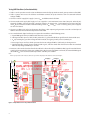
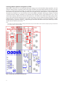
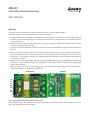
ACPL-337J
Isolated IGBT Gate Driver Evaluation board
User's Manual
Quick-Start
Visual inspection is needed to ensure that the evaluation board is received in good condition.
Default connections of the evaluation board are as shown (see Figure 1):
1. Q1 (Bipolar Buffer Driver), Q2 (Miller Clamp Bipolar) and Q3 (IGBT) are not mounted. An actual IGBT should be
mounted at Q3 (for TO-247 package), or connected to the driver board through short wire connections from the
holes provided at Q3.
2. CON3 is provided to allow for positive supply (VCC2) and negative supply (VEE2) with respect to VE (marked as E, which
is connected to emitter pin of the IGBT).
3. J1 jumper is shorted by default to connect the output to the Gate pin of the IGBT, through gate resistors R6 (10 Ω) &
R7 (0 Ω);
4. R9, R10 and Q1 (provisions for buffer driver) are not mounted by default. These components will be needed if more
than 4 A of gate drive current is required (J1 must be removed while R7 must then be shorted to accommodate this).
5. Similarly, Q2 is not mounted by default. This component should be mounted, however, if Miller Clamp current of
more than 2 A is required;
6. CON2 and J2 are shorted by default to allow for a single input PWM signal at Vin+ (pin 2 of CON1) to drive the LED of
ACPL-337J. If a separate LED drive signal (across R3 and R4) is required, then CON2 (and J2 if R4 cannot be grounded
to Gnd) must be opened.
7. CON1 is provided to allow for the power supply (+5V) to be connected across VCC1 and Gnd, TTL signal drive at Vin+,
direct driving of LED, plus /UVLO and /Fault feedback.
Component Side
Solder Side
Gnd
Vin+
Vcc1
/UVLO
/Fault
LED+
LED−
J2 shorted
CON2 shorted
J1 shorted
Figure 1. Actual ACPL-337J evaluation board showing default connections
Once inspection is done, the evaluation board can be powered up in seven simple steps, as shown in Figure 2, in simulation mode, without the need of actual IGBT.
Testing IGBT Gate Driver (in Simulation Mode)
1. Solder a 10 nF capacitor across the Gate and Emitter terminals of Q3 (to simulate actual gate capacitance of an IGBT).
2. Solder a jumper wire across the Collector and Emitter terminals of Q3 (to simulate a turn-on saturated Collector
voltage of IGBT).
3. Connect a +5V DC supply (DC supply 1) across VCC1 and GND terminals of CON1.
4. Connect another DC supply (DC Supply 2 of +15 V typical or +30 V maximum) across VCC2 (VCC2 pin) and VE (E pin)
terminals of CON3. Connect a third DC supply (DC Supply 3 of -5V typical or -15 V maximum) across VEE2 (VEE2 pin)
and VE (E pin) terminals of CON3. Maximum voltage across VCC2 and VEE2 is 30 V. For testing, these power supplies
can be non-isolated.
5. Connect a 10 kHz 5 V DC pulse (at about 50% duty) from a dual-output signal generator across IN+ and Gnd pins of
CON1 to simulate microcontroller output to drive the IGBT.
6. Use a multichannel digital oscilloscope to capture the waveforms at the following points:
a. Input PWM signal at IN+ pin (CON1) with reference to (w.r.t.) Gnd.
b. LED signal at LED+ pin w.r.t. Gnd (or LED-). Note: this is a generated LED drive signal from the device ACPL-337J.
c.VG representing the gate drive voltage of ACPL-337J (U1) at G (gate) pin of Q3 w.r.t. E (emitter) pin.
d. Desat signal at pin 14 of U1, which represents the Desat voltage of IGBT’s C (collector) pin during turn-on.
e. Confirm that LED+ signal is almost identical to IN+ signal, and then switch this channel to monitor the simulated
Miller Clamp voltage of IGBT at pin 10 of U1.
7. Provision is done on the board to allow for the LED to be driven directly by 5 V PWM (10 kHz) signals instead of the IN+
signal by disconnecting the shunt post at CON2. Once the shunt post at CON2 is removed, the external PWM signals
(at 10 kHz 5VPP) can be connected directly to LED+ and LED- pins at CON1.
Note:
Before you proceed to the next tests, make sure you remove the jumper wire that was connected in Step 2.
–5V
4
DC Supply 1
Gnd
3
Vin+ 6a
Vcc1
/UVLO
/Fault
6b
LED+
LED-
Figure 2. Simple Simulation Test Setup of Evaluation board
2
0V
+15V
5
DC Supply 3
Gnd
in+
+5V
Signal
Input
DC Supply 2
6d
6e
6c
1
10 nF
2
Jumper
Short
Schematics
Figure 3 shows the schematics of the evaluation board.
CON1
1 µF
C3 + T A
R2
R1
10k
1 VEE1
VEE2 16
2 VIN+
VLED 15
3 VCC1
DESAT 14
4 VLEDDRV
10k
5 UVLO
CON2
6 FAULT
VOUT 11
150
7 ANODE
VCLAMP 10
150
8 CATHODE
C2
330pF
R3
R4
J2
VCC2 12
VEE2
1 µF
C7 + T A
C
R5 1k
D1
VCC2
VE
1 kV
7,8
1
R6 2W
10
VEE2
9
C5 +
1 µF
TA
R9
J1
R10
Q1b
R7 2W
0R
Q3
C
(TO247)
G
3
nm R8 47
3
PBSS4041SPN 5,6
1
Q2 nm4,2
2STN2540
nm :Not Mounted
Figure 3. Schematics of the ACPL-337J evaluation board
nm
BYV26E
Q1a nmPBSS4041SPN
2
Gnd
3
E
VE
C6
100pF
1 µF
C4 + T A
G
nm
C1
330pF
VCC2
SBD
BAT42W
VE 13
CON4
CON3
nm
Gnd
4
V EE2
nm
E
VE
Practical Connections of the Evaluation board Using Power MOSFET for Actual Inverter Test
1. Solder an actual IGBT at Q3 by following the pins marked as G (gate), C (collector) and E (emitter).
2. Connect a +5V DC supply (DC supply 1) across VCC1 and GND terminals of CON1.
3. Connect another DC supply (DC Supply 2 of +15V) across VCC2 (VCC2 pin) and VE (E pin) terminals of CON3. Connect
a third DC supply (DC Supply 3 of -5V typical or -15V max) across VEE2 (VEE2 pin) and VE (E pin) terminals of CON3.
Maximum voltage across VCC2 and VEE2 is 30 V. These two DC power supplies must be isolated from DC Supply 1.
4. Connect the PWM output signals(meant to drive the IGBT) from microcontroller to input signals at IN+ and Gnd pins
of CON1; Connect also the /UVLO and /Fault from CON1 to the same microcontroller at designated feedback pins.
4
Microcontroller
IN+
–5 V
0V
DC Supply 3
3
Gnd
DC Supply 2
2
6
HV+
IGBT
Gnd
Vin+ 5a
Vcc1
/UVLO
/Fault
5c
1
Inductive Load
Gnd
DC Supply 1
+5V
+15 V
5. Use a multi-channel Digital Oscilloscope to capture the waveforms at the following points:
a. Input PWM signal at IN+ pin (CON1) with reference to (w.r.t.) Gnd
b.VG representing the gate drive voltage of ACPL-337J (U1) at G (gate) pin of Q3 w.r.t. E (emitter) pin. Monitoring of
this signal must be done through a HV differential probe
c. Desat signal at pin 14 of U1 represents the Desat voltage of IGBT’s C (collector) pin during turn-on. Monitoring of
this signal must be done through a HV differential probe
d. Miller Clamp voltage of IGBT at pin 10 of U1. Monitoring of this signal must be done through a HV differential
probe
6. Connect C (collector) pin of the IGBT to HV+ (High Voltage DC Bus+) through a properly selected Inductive Load.
Connect E (emitter) pin of the IGBT to HV- (High Voltage DC Bus-). (Note: It is advised to enable the current limiting
function of the HV Power Source supplying the High Voltage DC Bus voltage during this test to protect the Inverter
and its drive circuits). Maximum voltage allowed across HV+ and HV- is 1 kV for the board.
5b
5d
O/P
LED+
LED
HV–
Figure 4. Connection of evaluation board in actual applications
4
Application Circuit Description
The ACPL-337J is an isolated gate driver that provides >4 A output current. The voltage and high peak output current
supplied by this optocoupler make it ideally suited for direct driving of IGBT with ratings up to 1000 V/100 W. It is also
designed to drive different sizes of buffer stage that will make the class of IGBT scalable. ACPL-337J provides a single
isolation solution suitable for both low power and high power ratings of motor control and inverter applications.
Each of the ACPL-337J evaluation boards, as shown in Figure 5, accommodates an ACPL-337J IC. The board is enough
to drive an Inverter arm. This allows the designer to easily test the performance of gate driver in an actual application
solution. Operation of the evaluation board requires just the inclusion of a common 5V DC isolated Supply1 on the input
side and two isolated DC supplies on the output side, together with a PWM drive signal from the microcontroller.
Provision is done on the board to allow for the LED to be driven either directly by external 5V PWM (10 kHz) signals or
the generated LED signal, by disconnecting or connecting the shunt post at CON2, respectively. By default, the LED
is driven by the internally generated LED drive signal (LEDDRV pin 4 at U1). Once the shunt post at CON2 is removed,
external PWM signals (at 5VPP 10 kHz) can be connected directly to LED+ and LED- pins at CON1 to drive the LED of the
optocoupler through the onboard current limiting resistors. This provision is to provide the designer flexibility.
Once the LED is driven by a signal current (typically 11.5 mA), output at pin 11 is activated with a positive pulse voltage and ready to drive the IGBT’s gate through a gate resistor R6 (10 Ω). Assuming that the voltage supply at VCC2 and
VEE w.r.t. VE (or E) are +15V and -5V respectively, the maximum drive current is limited to 2 A peak (= (VCC2 – VEE)/RG). If
needed, RG can be reduced to accommodate up to 4 A of peak output drive current allowable by the specification. But
care must be taken to ensure that junction temperature of the device is always below 125 °C.
ACPL-337J is a smart gate driver with many integrated protection features such as:
a. IGBT collector desaturation fault protection against overload as well as short circuit,
b. Preventing false turn-on due to Miller current effect, and
c. UVLO to prevent premature output turn-on due to insufficient supply voltage.
Desat Protection
For normal loading during IGBT turn-on, the collector saturation voltage should fall below 5V (= Vdesat – Iconstant *
Rdesat – VF), where
Vdesat = 7V typical (protection threshold of Desat voltage)
Iconstant = 1 mA of internal constant current source
Rdesat = 1 kΩ of R5
VF
= 1V (typical) of D1 for BYV26E at 1 mA
During overload or short circuit, the collector saturation voltage is higher than 5 V and the detected voltage at the Desat
pin 14 of U1 will be higher than 7 V. This will trigger output shutdown (output soft shutdown will be initiated and at the
same time the /Fault feedback pin 6 will be pulled low to inform external microcontroller that there is a Fault happening
at the IGBT power switch) to turn off the IGBT to protect it from damage. So the IGBT should be selected such that its
collector saturation voltage during turn-on under full load condition is less than 5 V. If the collector saturation voltage
during full load is too low, e.g., < 3 V, then adding a 2 V Zener between R5 and diode D1 would definitely help to provide
proper overload or short circuit protection.
For other design criteria for Desat protection, refer to the application notes.
Preventing false turn-on by Miller effect
Every IGBT used will have a junction capacitance between collector and gate (or Miller capacitance). Ideally, this capacitance has to be as small as possible, but it can never be eliminated. This Miller capacitance might allow transient current
to flow from collector to gate and causes the gate voltage to rise during gate turn-off duration. If this sudden surge of
gate voltage is higher than the gate threshold voltage (usually 2~5V), a false IGBT turn-on might happen.
To prevent this, the IGBT gate voltage is monitored (by connecting it to the Clamp pin 10 of U1) during the turn-off duration. During turn-off, the gate voltage, as monitored, is pulled low and it will drop from VCC2 level to VEE2 level. As soon
as this gate voltage level drops below 2 V w.r.t. VEE2, an internal clamp is activated to shunt the Clamp pin 10 to pin 9,
which is at VEE2 level. By doing so, it ensures that the gate voltage has no chance of getting over 2 V again during the
entire IGBT off duration. Monitoring of this pin 10 will notice a sudden dip in voltage from 2 V (typically) to 0 V immediately, to confirm that the active Miller Clamp is working properly.
Note: As an active Miller clamp is built-in to this ACPL-337J device, negative supply is not needed, and VE and VEE2 can be shorted.
5
Preventing premature output turn-on through the use of UVLO
When IGBT is allowed to turn on immediately after gate voltage crosses the threshold voltage (typically 2~5V), the
collector emitter junction is operating at the linear region. This will cause high voltage built-up across the very same
junction, especially when the load is high. The conduction power dissipation (=load current * junction voltage) of the
device will be very high and it will be damaged if this power is higher than the allowable limit. To prevent high power
dissipation, the designer has to ensure that the turn-on of the IGBT is prohibited until the gate voltage has reached
a certain level where collector saturation can be reached, and usually this calls for a gate voltage to be >12 V. This is
achieved by including a UVLO circuit inside the ACPL-337J device. This UVLO circuit monitors the supply voltage at VCC2
w.r.t. VE, and it will not allow output to be turn-on until VCC2 voltage crosses the UVLO+ threshold, typically 12.3 V. The
UVLO protection circuit can be checked by varying VCC2 supply voltage higher than or lower than the UVLO+ or UVLOthreshold voltage, respectively. When VCC2 supply voltage is lower than the UVLO- threshold, the /UVLO at pin 6 of U1
should send out a low level, w.r.t. Gnd.
Note:
As can be seen on the board, the isolation circuitry (at the far left) is easily contained within a small area while adequate spacing is maintained for
good voltage isolation and easy assembly.
Figure 5. Top and bottom views of ACPL-337J evaluation board
6
Using the Board
The evaluation board is easily prepared for use. Only minor preparations (just by soldering cables for DC supplies, input
PWM & /Fault + /UVLO feedback signals, proper cables for HV+/HV- high voltage bus, and load connections) are required. The evaluation board is having a default connection as shown in Table1 when shipped to customer. Customer is
free to select a different LED driving schemes and whether negative supply is used, as shown in the Table.
Table 1
VCC2
VEE2
LED is
No. driven by
CON2
VCC1
1
VLEDDRV
s/c
+5 V
External
+15V~30V
External
0V ~ -15V
External
2
VLEDDRV
s/c
+5 V
External
+15V~30V
External
s/c
0V
3
Microcontroller
(external)
open
+5 V
External
+15V~30V
External
0 V ~ -15 V
External
4
Microcontroller
(external)
open
+5 V
External
+15V~30V
External
s/c
0V
30 V maximum
VE
J1
J2
Remarks
0V
s/c
s/c
Default
–3 external supplies needed for VCC1, VCC2
and VEE2
s/c
*1
Simplest
–2 external supplies needed for VCC1 &
VCC2
s/c
s/c
LED’s driven externally
–3 external supplies needed for VCC1,
VCC2a & VCC2b
s/c
*1
LED’s driven externally
–2 external supplies needed for VCC1 &
VCC2
0V
Notes:
*1. Whether J2 can be shorted depends on the drive signals (for connection to LED+ and LED-) from the Microcontroller.
*2. Since Miller Clamp function is built-in, -ve supply for VEE2 can be omitted, so VEE2 can be shorted to VE externally.
Note:
As the Desat diode’s breakdown voltage is rated at 1k V, IGBT must be selected with VCES <1 kV, and maximum HV+ voltage plus flyback voltage of
load inductor must be <1 kV).
7
Output Measurement
A sample of Input signal and various output waveforms are captured and shown in Figure 6, during IGBT gate turn-off
and turn-on instants. Default setup connection is used but with Q3 IGBT mounted. The IGBT used has a gate capacitance equivalent to 10 nF. It is noticed that during normal working condition, the Desat pin voltage is much less than 7
V, and no Fault occurs.
For the exploded view, see Figure 7.
Figure 6. ACPL-337J Input and output plus protection signal waveforms
2V
Figure 7. Exploded view of Active Miller Clamp pin waveform at turn-off
Figure 7 is the exploded view of the Miller Clamp pin-10 waveform during turn-off duration, it shows clearly that once
the detected Gate voltage drops below 2 V (typically), the Gate voltage is shunt and clamped to 0 V w.r.t. VEE2 level during the entire turn-off duration, to ensure that the Gate voltage has no chance of going above the turn-on threshold
level again.
8
Fault Feedback
DesatFault detected
Figure 8 shows the actual Desat 7 V threshold detection that triggers the VG output soft-shutdown as well as /Fault feedback pin voltage is pulled low to inform microcontroller that a fault has been detected.
7V
Figure 8. Desat Protection & Fault Feedback
Figure 9 shows that the VCC2 voltage sag below UVLO- level (between 11~12 V) triggers the UVLO and shutdown the
output VG level and recovers after normal VCC2 voltage recovers above UVLO+ level (between 12~13 V). The /UVLO pin
voltage is also pulled low throughout the same duration to inform the microcontroller that severe VCC2 level drop has
happened.
VCC2
VCC2 undervoltage detected
/UVLO
UVLO reported
15V 14V 13V
12V 11V
VCC2 ’Normal’ detected
VIN+
VG output
12V 13V 14V
15V
Figure 9. UVLO Feedback
In conclusion, with these sophisticated IGBT gate driving and driver protection schemes built-in, ACPL-337J is well suited
for modern IGBT applications such as Motor Control and Voltage inverters.
For product information and a complete list of distributors, please go to our web site:
www.avagotech.com
Avago, Avago Technologies, and the A logo are trademarks of Avago Technologies in the United States and other countries.
Data subject to change. Copyright © 2005-2014 Avago Technologies. All rights reserved.
AV02-4404EN - February 6, 2014