1
To our customers,
Old Company Name in Catalogs and Other Documents
On April 1st, 2010, NEC Electronics Corporation merged with Renesas Technology
Corporation, and Renesas Electronics Corporation took over all the business of both
companies. Therefore, although the old company name remains in this document, it is a valid
Renesas Electronics document. We appreciate your understanding.
Renesas Electronics website: http://www.renesas.com
April 1st, 2010
Renesas Electronics Corporation
Issued by: Renesas Electronics Corporation (http://www.renesas.com)
Send any inquiries to http://www.renesas.com/inquiry.
Notice
1.
2.
3.
4.
5.
6.
7.
All information included in this document is current as of the date this document is issued. Such information, however, is
subject to change without any prior notice. Before purchasing or using any Renesas Electronics products listed herein, please
confirm the latest product information with a Renesas Electronics sales office. Also, please pay regular and careful attention to
additional and different information to be disclosed by Renesas Electronics such as that disclosed through our website.
Renesas Electronics does not assume any liability for infringement of patents, copyrights, or other intellectual property rights
of third parties by or arising from the use of Renesas Electronics products or technical information described in this document.
No license, express, implied or otherwise, is granted hereby under any patents, copyrights or other intellectual property rights
of Renesas Electronics or others.
You should not alter, modify, copy, or otherwise misappropriate any Renesas Electronics product, whether in whole or in part.
Descriptions of circuits, software and other related information in this document are provided only to illustrate the operation of
semiconductor products and application examples. You are fully responsible for the incorporation of these circuits, software,
and information in the design of your equipment. Renesas Electronics assumes no responsibility for any losses incurred by
you or third parties arising from the use of these circuits, software, or information.
When exporting the products or technology described in this document, you should comply with the applicable export control
laws and regulations and follow the procedures required by such laws and regulations. You should not use Renesas
Electronics products or the technology described in this document for any purpose relating to military applications or use by
the military, including but not limited to the development of weapons of mass destruction. Renesas Electronics products and
technology may not be used for or incorporated into any products or systems whose manufacture, use, or sale is prohibited
under any applicable domestic or foreign laws or regulations.
Renesas Electronics has used reasonable care in preparing the information included in this document, but Renesas Electronics
does not warrant that such information is error free. Renesas Electronics assumes no liability whatsoever for any damages
incurred by you resulting from errors in or omissions from the information included herein.
Renesas Electronics products are classified according to the following three quality grades: “Standard”, “High Quality”, and
“Specific”. The recommended applications for each Renesas Electronics product depends on the product’s quality grade, as
indicated below. You must check the quality grade of each Renesas Electronics product before using it in a particular
application. You may not use any Renesas Electronics product for any application categorized as “Specific” without the prior
written consent of Renesas Electronics. Further, you may not use any Renesas Electronics product for any application for
which it is not intended without the prior written consent of Renesas Electronics. Renesas Electronics shall not be in any way
liable for any damages or losses incurred by you or third parties arising from the use of any Renesas Electronics product for an
application categorized as “Specific” or for which the product is not intended where you have failed to obtain the prior written
consent of Renesas Electronics. The quality grade of each Renesas Electronics product is “Standard” unless otherwise
expressly specified in a Renesas Electronics data sheets or data books, etc.
“Standard”:
8.
9.
10.
11.
12.
Computers; office equipment; communications equipment; test and measurement equipment; audio and visual
equipment; home electronic appliances; machine tools; personal electronic equipment; and industrial robots.
“High Quality”: Transportation equipment (automobiles, trains, ships, etc.); traffic control systems; anti-disaster systems; anticrime systems; safety equipment; and medical equipment not specifically designed for life support.
“Specific”:
Aircraft; aerospace equipment; submersible repeaters; nuclear reactor control systems; medical equipment or
systems for life support (e.g. artificial life support devices or systems), surgical implantations, or healthcare
intervention (e.g. excision, etc.), and any other applications or purposes that pose a direct threat to human life.
You should use the Renesas Electronics products described in this document within the range specified by Renesas Electronics,
especially with respect to the maximum rating, operating supply voltage range, movement power voltage range, heat radiation
characteristics, installation and other product characteristics. Renesas Electronics shall have no liability for malfunctions or
damages arising out of the use of Renesas Electronics products beyond such specified ranges.
Although Renesas Electronics endeavors to improve the quality and reliability of its products, semiconductor products have
specific characteristics such as the occurrence of failure at a certain rate and malfunctions under certain use conditions. Further,
Renesas Electronics products are not subject to radiation resistance design. Please be sure to implement safety measures to
guard them against the possibility of physical injury, and injury or damage caused by fire in the event of the failure of a
Renesas Electronics product, such as safety design for hardware and software including but not limited to redundancy, fire
control and malfunction prevention, appropriate treatment for aging degradation or any other appropriate measures. Because
the evaluation of microcomputer software alone is very difficult, please evaluate the safety of the final products or system
manufactured by you.
Please contact a Renesas Electronics sales office for details as to environmental matters such as the environmental
compatibility of each Renesas Electronics product. Please use Renesas Electronics products in compliance with all applicable
laws and regulations that regulate the inclusion or use of controlled substances, including without limitation, the EU RoHS
Directive. Renesas Electronics assumes no liability for damages or losses occurring as a result of your noncompliance with
applicable laws and regulations.
This document may not be reproduced or duplicated, in any form, in whole or in part, without prior written consent of Renesas
Electronics.
Please contact a Renesas Electronics sales office if you have any questions regarding the information contained in this
document or Renesas Electronics products, or if you have any other inquiries.
(Note 1) “Renesas Electronics” as used in this document means Renesas Electronics Corporation and also includes its majorityowned subsidiaries.
(Note 2) “Renesas Electronics product(s)” means any product developed or manufactured by or for Renesas Electronics.
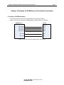
Application Note
Multimedia Processor for Mobile Applications
SD Memory Card Interface
--------------------------------------------------------------------------------------
EMMA Mobile1
Document No.
Date Published
S19895EJ1V0AN00
Aug. 2009
2009
Printed in Japan
PREFACE
PREFACE
Purpose
The purpose of this document is to specify the usage of EMMA Mobile1
SD Memory Card (SDM) interface.
Organization
This document includes the following:
Introduction
Usage of SDM Interface
Example of SDM Operation
SD Driver Function
Notation
Here explains the meaning of following words in text:
Related document
Note
Explanation of item indicated in the text
Caution
Information to which user should afford special attention
Remark
Supplementary information
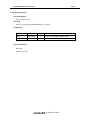
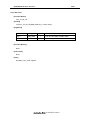
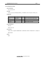
The following tables list related documents.
Reference Document
Document Name
Version/date
Author
Description
S19265EJ1V0UM00_ASMUGIO.pdf
1st Edition
NECEL
SMU&GPIO user’s manual
S19268EJ1V0UM00_1chip.pdf
1st Edition
NECEL
1 chip user’s manual
S19361JJ2V0UM00_SDI.pdf
2nd Edition
NECEL
S19907EJ1V0AN00_GD.pdf
1stEdition
NECEL
SDM
interface
manual
GD spec
Application Note S19895EJ1V0AN00
user’s
PREFACE
Disclaimers
The information contained in this document is subject to change without prior
notice in the future. Refer to the latest applicable data sheet(s) and user manual
when designing a product for mass production.
No part of this document may be copied or reproduced in any form or by any means
without the prior written consent of NEC Electronics. NEC Electronics assumes no
responsibility for any errors that may appear in this document.
NEC Electronics does not assume any liability for infringement of patents, copyrights or
other intellectual property rights of third parties by or arising from the use of NEC
Electronics products listed in this documents or any other liability arising from the use of
such products. No license, express, implied or otherwise, is granted under any patents,
copyrights or other intellectual property rights of NEC Electronics or others.
Descriptions of circuits, software and other related information in this document are
provided for illustrative purposes in semiconductor product operation and application
examples. The incorporation of these circuits, software and information in the design of a
customers’ equipment shall be done under the full responsibility of the customer. NEC
Electronics assume no responsibility for any losses incurred by customers or third parties
arising from the use of these circuits, software and information.
While NEC Electronics endeavors to enhance the quality, reliability and safety of NEC
Electronics products, customers agree and acknowledge that possibility of defects thereof
cannot be eliminated entirely. To minimize risks of damage to property or injury (including
death) to persons arising from defects in NEC Electronics products, customers must
incorporate sufficient safety measures in their design, such as redundancy, firecontainment and anti-failure features.
Note)
1. “NEC Electronics” as used in this document means NEC Electronics Corporation and also
includes its majority-owned subsidiaries.
2. “NEC Electronics products” means any product developed or manufactured by or for NEC
Electronics (as defined above)
3. All trademarks or registered trademarks are the property of their respective owners.
Registered trademarks ® and trademarks™ are not noted in this document.
Application Note S19895EJ1V0AN00
INDEX
4/52
CONTENTS
Chapter 1 Introduction ................................................................................................................. 7
1.1 Outline .................................................................................................................................... 7
1.2 Development Environment..................................................................................................... 7
Chapter 2 Usage of SD Memory Card Interface......................................................................... 8
2.1 Initialization............................................................................................................................. 9
2.2 Data Transfer.........................................................................................................................11
2.3 Erase .................................................................................................................................... 14
Chapter 3 Example of SD Memory Card Interface Operation.................................................. 15
3.1 Outline of SDM Operation .................................................................................................... 15
3.2 Initialization........................................................................................................................... 16
3.2.1 Operation Flow .............................................................................................................. 16
3.2.2 Operation Detail............................................................................................................. 17
3.3 Example of SDM Single Block Read/Write .......................................................................... 20
3.3.1 Operation Flow .............................................................................................................. 20
3.3.2 Operation Detail............................................................................................................. 21
3.4 Example of SDM Multi Block Operation............................................................................... 23
3.4.1 Operation Flow .............................................................................................................. 23
3.4.2 Operation Detail............................................................................................................. 25
APPENDIX A SD Driver Function ............................................................................................... 26
A.1 Function List......................................................................................................................... 26
A.2 Global Variable Define ......................................................................................................... 26
A.3 Structure & Enum Define ..................................................................................................... 27
A.3.1 mmc_csd ....................................................................................................................... 27
A.4 Function Details ................................................................................................................... 28
A.4.1 Hardware Initialization Function................................................................................... 28
A.4.2 Card Init Operation........................................................................................................ 29
A.4.3 Sector Setting................................................................................................................ 31
A.4.4 Send Command ............................................................................................................ 32
A.4.5 Set Clock....................................................................................................................... 34
A.4.6 Set Block Length ........................................................................................................... 35
A.4.7 Select Card ................................................................................................................... 36
A.4.8 Check Device Status ..................................................................................................... 37
A.4.9 Erase Function .............................................................................................................. 39
A.4.10 Single Block Read....................................................................................................... 40
A.4.11 Single Block Write ....................................................................................................... 42
A.4.12 Multiple Block Read .................................................................................................... 44
A.4.13 Multiple Block Write..................................................................................................... 45
A.4.14 Transfer Prepare ......................................................................................................... 46
A.4.15 Decode CSD ............................................................................................................... 47
Application Note S19895EJ1V0AN00
INDEX
5/52
A.4.16 Check Response Status.............................................................................................. 48
APPENDIX B COMMANDS .......................................................................................................... 49
ANNEX Modification History....................................................................................................... 52
Application Note S19895EJ1V0AN00
INDEX
6/52
LIST OF TABLES
Table 1-1 Hardware Environment ....................................................................................... 7
Table 1-2 Software Environment......................................................................................... 7
Table A-1 SD Driver Function List..................................................................................... 26
Table A-2 Global Variable Define...................................................................................... 26
Table A-3 Structure Define................................................................................................ 27
Table A-4 Structure of mmc_csd....................................................................................... 27
Table B-1 Command Description List ............................................................................... 49
LIST OF FIGURES
Figure 2-1 EMMA Mobile 1 SDM Initialization .................................................................... 9
Figure 2-2 EMMA Mobile 1 SDM Data Transfer in DMA Mode ........................................ 11
Figure 2-3 EMMA Mobile 1 SDM Erase Operation ........................................................... 14
Figure 3-1 Connection between EMMA Mobile 1 and SD card ........................................ 15
Figure 3-2 Initialization before Test................................................................................... 16
Figure 3-3 SDM Single Read/Write Operation Flow ......................................................... 20
Figure 3-4 SD Multi block Operation Flow ........................................................................ 23
Figure A-1 SDM Hardware Initialization Flow ................................................................... 28
Figure A-2 SD card Initialization Flow ............................................................................... 30
Figure A-3 Sector Setting Flow ......................................................................................... 31
Figure A-4 Send Command .............................................................................................. 33
Figure A-5 Set Block Length ............................................................................................. 35
Figure A-6 Select Card...................................................................................................... 36
Figure A-7 Check Card Stauts .......................................................................................... 38
Figure A-8 Single Block Read in CPU mode .................................................................... 41
Figure A-9 Single Block Write in CPU mode..................................................................... 43
Figure A-10 Register Prepare before Data transfer .......................................................... 46
Figure A-11 Check Response Status................................................................................ 48
Application Note S19895EJ1V0AN00
Chapter 1 Introduction
7/52
Chapter 1 Introduction
1.1 Outline
This document will show users how to operate SD memory card interface on EMMA Mobile1
evaluation board.
1.2 Development Environment
Hardware environment of this project is listed as below.
Table 1-1 Hardware Environment
Name
Version
Maker
EMMA Mobile 1 evaluation board (PSKCH2YS-0016-01)
-
NEC Electronics
M20
Kyoto Microcomputer Co. Ltd
PARTNER-Jet ICE ARM
Software used in this project is listed as below.
Table 1-2 Software Environment
Version
Maker
GNUARM Toolchain
Name
V4.3.2
GNU
WJETSET-ARM
V5.10a
Kyoto Microcomputer Co. Ltd
Application Note S19895EJ1V0AN00
Chapter 2 Usage of SD Memory Card Interface
8/52
Chapter 2 Usage of SD Memory Card Interface
According to the hardware feature, the EMMA Mobile 1 SD memory card (SDM) interface has the
following main function:
1. Initialization
2. Data Transfer
3. Erase
Application Note S19895EJ1V0AN00
Chapter 2 Usage of SD Memory Card Interface
9/52
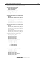
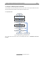
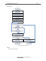
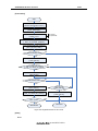
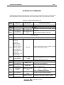
2.1 Initialization
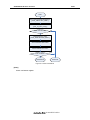
Following figure shows EMMA Mobile 1 SD initialize progress:
Start
Power on
Clock and Reset setting about
SDM module
Switch GPIO to SD function and
Setting pull-up/pull-down for SD
Wait/Read/Driver ability and Auto
frequency configuration
Software reset SD
Setting bus width and response
time out value
Clear and mask all info
Enable and setting clock (in low
frequency)
Send CMD 0, setting EMMC
device into idle state
Send CMD 55 and CMD41,
setting device into ready state
Get CID info(CMD 2) and setting
relative address(CMD 3) for all
devices in bus
ASMU_GCLKCTRL4ENA
ASMU_GCLKCTRL4
ASMU_RESETREQ3
ASMU_RESETREQ3ENA
Note1
ASMU_AB1_SDIxWAITCTRL
ASMU_AB1_SDIxREADCTRL
CHG_DRIVE1
ASMU_AUTO_FRQ_MASK3
SDIx_SOFT_RST
SDIx_OPTION
Note2
SDIx_INFO1
SDIx_INFO2
SDIx_INFO1_MASK
SDIx_INFO2_MASK
SDIx_CLK_CTRL Note3
SDIx_CMD Note4
SDIx_ARG0
SDIx_ARG1
SDIx_CMD
Note5
Get CSD info from device(CMD 9)
Select device (CMD 7)
Set block size (CMD 16)
Setting transfer bus width and
speed (CMD55 and CMD 6)
End
Figure 2-1 EMMA Mobile 1 SDM Initialization
Note:
1) Switch pins to SD function, users should operate this step according the actual hardware
Application Note S19895EJ1V0AN00
Chapter 2 Usage of SD Memory Card Interface
10/52
connection, for example: if users connect the SD card with SD1 interface, please switch the
related GPIO to SD1 function.
2) Before the initialization of SD card, set the bus width to be 1bit and the response time out
value to be maximum, reason is: in SD card identification progress, bus width will use 1bit and
the clock frequency should in 10-400 KHz range.
3) After setting the clock for SDM transfer, please wait 1ms for stability.
4) After send command, user should check the command response, if error occurred (except
when response time out for CMD 2), the initialization will be ended abnormally.
Commands simple description please refers to the “APPENDIX B COMMANDS”.
5) CID: Card Identification
CSD: Card Specific Data
6) After initialization, users can configure the bus width and clock frequency for transfer speed
according the CSD parameter of SD card, the transfer speed defines in CSD register just clock
frequency not in high speed mode, so the actual transfer speed is related to SD card
specification version.
7) The register name SDIx described in this document means the SDIA, SDIB or SDIC, which can
be changed according the hardware connection, more details about SDM registers and related
bits please refer to SDM interface user’s manual of EMMA Mobile 1.
Application Note S19895EJ1V0AN00
Chapter 2 Usage of SD Memory Card Interface
11/52
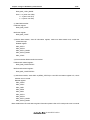
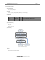
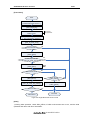
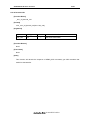
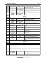
2.2 Data Transfer
SD memory card interface has two kinds of data transfer mode: DMA mode and CPU mode. In
realize operation, mainly use DMA mode to transfer data, so in this chapter, introduce the DMA
mode operation, about SD single block read/write in CPU mode; please refer to “APPENDIX A
SD Driver Function”.
Following figure shows EMMA Mobile 1 SD DMA read/write progress:
Start
Wait for SD card interface not
busy
Enable SDM DMA mode
DMA init and transfer setting
SDIx_INFO2[14]
SDIx_CC_EXT_MODE
Note1
Note2
Start DMA
Set sector enable and sector
number to be transfered
SDIx_STOP
SDIx_SECCNT
Note3
Transfer prepare
Send read/ write command
No
DMA transfer end?
Note4
SDIx_INFO1[2 ]
Yes
Yes
R/W transfer end?
No
No
Check whether error occuer
There is still data
to be transfer?
Clear transfer info and disable
Yes
DMA mode
Disable sector
SDIx_INFO2
SDIx_INFO1
SDIx_INFO2
SDIx_CC_EXT_MODE
SDIx_STOP
Resetting DMA transfer parameter
Check SD card status
Note5
Restart DMA for the left data
End
Figure 2-2 EMMA Mobile 1 SDM Data Transfer in DMA Mode
Note:
1) In DMA init and transfer setting step, user should reset DMA channel, open DMA clock, clear
Application Note S19895EJ1V0AN00
Chapter 2 Usage of SD Memory Card Interface
DMA interrupt source, set transfer parameter for DMA.
DMA reset setting related register:
ASMU_RESETREQ0ENA
ASMU_RESETREQ0
DMA clock setting related register:
ASMU_GCLKCTRL0
ASMU_GCLKCTRL0ENA
P2M Clear DMA interrupt source related register:
For SD0:
DMA_P2M_PE0_LCH0LCH3_INT_REQ_CL
DMA_P2M_DSP_LCH0LCH3_INT_REQ_CL
For SD1 and SD2:
DMA_P2M_PE0_LCH4LCH7_INT_REQ_CL
DMA_P2M_DSP_LCH4LCH7_INT_REQ_CL
M2P Clear DMA interrupt source related register:
For SD0:
DMA_M2P_PE0_LCH0LCH3_INT_REQ_CL
DMA_M2P_DSP_LCH0LCH3_INT_REQ_CL
For SD1 and SD2:
DMA_M2P_PE0_LCH4LCH7_INT_REQ_CL
DMA_M2P_DSP_LCH4LCH7_INT_REQ_CL
P2M DMA transfer setting related register:
DMA_P2M_LCHx_AADD
DMA_P2M_LCHx_BADD
DMA_P2M_LCHx_BOFF
DMA_P2M_LCHx_BSIZE
DMA_P2M_LCHx_BSIZE_COUNT
DMA_P2M_LCHx_LENG
DMA_P2M_LCHx_MODE
Here x = 3 (when use SD0)
x = 4 (when use SD1)
x = 5 (when use SD2)
M2P DMA transfer setting related register:
DMA_M2P_LCHx_BADD
DMA_M2P_LCHx_AADD
DMA_M2P_LCHx_AOFF
DMA_M2P_LCHx_ASIZE
DMA_M2P_LCHx_ASIZE_COUNT
DMA_M2P_LCHx_LENG
Application Note S19895EJ1V0AN00
12/52
Chapter 2 Usage of SD Memory Card Interface
13/52
DMA_M2P_LCHx_MODE
Here x = 3 (when use SD0)
x = 4 (when use SD1)
x = 5 (when use SD2)
2) Start DMA transfer.
P2M start register
DMA_P2M_CONT
M2P start register
DMA_M2P_CONT
3) Before data transfer, clear all information register, make sure data transfer end, enable the
related interrupt.
Related register:
SDIx_INFO1
SDIx_INFO2
SDIx_INFO1_MASK
SDIx_INFO2_MASK
SDIx_STOP
4) Check whether DMA transfer has ended
P2M transfer related register:
DMA_P2M_CONTSTATUS
M2P transfer related register:
DMA_M2P_CONTSTATUS
5) After data transfer, send CMD 13(SEND_STATUS) to read SD card status register info, check
whether error occurred.
Related register:
SDIx_ARG0
SDIx_ARG1
SDIx_CMD
SDIx_RSP0
SDIx_RSP1
SDIx_INFO1
SDIx_INFO2
SDIx_INFO1_MASK
SDIx_INFO2_MASK
More details about SD card status register information please refer to SD card product user’s manual.
Application Note S19895EJ1V0AN00
Chapter 2 Usage of SD Memory Card Interface
14/52
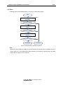
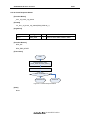
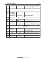
2.3 Erase
Following figure shows EMMA Mobile 1 SD memory card erase progress:
Start
Note 1
Send CMD 32 for erase group
start setting
Send command OK?
No
Yes
Send CMD 33 for erase group end
setting
Send command OK?
No
Yes
Send CMD 38 to execute erase
operation
Send command OK?
No
Yes
Normal End
Error End
Figure 2-3 EMMA Mobile 1 SDM Erase Operation
Note:
1)Parameter about CMD 32, CMD33 will be the address to start and end, the address will be in
Group erase unit, more details about erase operation and meaning of erase group unit please
refer to SD card product user’s manual.
Application Note S19895EJ1V0AN00
Chapter 3 Example of SD Memory Card Interface Operation
15/52
Chapter 3 Example of SD Memory Card Interface Operation
3.1 Outline of SDM Operation
This chapter will show users how to operate SD card using SD0 interface.
Figure 3-1 shows the connection of EMMA Mobile 1 SDM interface and SD card.
SD Card
EMMA Mobile1
DAT4~7
SD0_DATA3
DAT3
SD0_DATA2
DAT2
SD0_DATA1
DAT1
SD0_DATA0
DAT0
SD0_CMD
CMD
SD0_CKO
CLK
Figure 3-1 Connection between EMMA Mobile 1 and SD card
Application Note S19895EJ1V0AN00
Chapter 3 Example of SD Memory Card Interface Operation
16/52
3.2 Initialization
Before SD card operation, initialization should be executed at first.
3.2.1 Operation Flow
Start
Init hardware interface
[ em1_sd_hw_init() ]
Init SD card
[ em1_sd_init() ]
Init OK?
No
Yes
End
Error End
Figure 3-2 Initialization before Test
More details about the functions used in initialization please refer to “APPENDIX A SD Driver
Function”
Application Note S19895EJ1V0AN00
Chapter 3 Example of SD Memory Card Interface Operation
17/52
3.2.2 Operation Detail
(1) Init SDM module hardware
Init SDM module (function: em1_sd_hw_init() ).
Following steps shows the hardware initialization (em1_sd_hw_init()) progress:
Step1: Reset setting
ASMU_RESETREQ3[2]
ASMU_RESETREQ3ENA [2]
(0: reset; 1: cancel reset)
(0: disable setting; 1: enable setting)
Step2: Clock setting
ASMU_GCLKCTRL4[5]
(0: close clock; 1: open clock)
ASMU_GCLKCTRL4ENA[5]
(0: disable setting; 1: enable setting)
Step3: Switch pins to SD function:
CHG_PINSEL_G80 = 0x00550000 (GIO_P88-P91 -> SD0_DAT1-3, SD0_CKI)
CHG_PINSEL_SD0 = 0x00000001 (Switch the SD0_DATA1 to DATA3 and SD0_CKI
pins by using GIO_P88 to GIO_P91)
Step4: Pull-up/down setting
CHG_PULL_G88 = 0x00006666
(DATA1-3: Pull-down , mask release)
CHG_PULL2 = 0x00004663
(CKO: Pull release
CMD, DATA0: Pull-up, mask release)
Step5: Drive capability setting
CHG_DRIVE1 = 0x00050000
(SD0_CK and SD0 pins : 4mA, default value)
Setp6: Read and wait control register setting
ASMU_AB1_SDIAWAITCTRL = 0x00000300
ASMU_AB1_SDIAREADCTRL = 0x00000000 (default value)
Setp7: Auto frequency control setting
ASMU_AUTO_FRQ_MASK3 = 0x07 (default value)
(2) Init SD Card
SD card initialization (em1_sd _init()) including following steps:
Step1: Power on SD card
Step2: Soft reset SD
SDIA_SOFT_RST = 0x0000
(module reset)
SDIA_SOFT_RST = 0x0007
(release reset)
Application Note S19895EJ1V0AN00
Chapter 3 Example of SD Memory Card Interface Operation
18/52
Step3: Set bus width and time out value for response, card detect stable time
SDIA_OPTION = 0x80EE
(bus width: 1bit; biggest time value for response time
out and card detection stable time )
Step4: Clear and mask all information and interrupt
SDIA_INFO1 = 0x0000
SDIA_INFO2 = 0x0000
SDIA_INFO1_MASK = 0xFFFF
SDIA_INFO2_MASK = 0xFFFF
Step5: Set clock
SDIA_CLK_CTRL = 0x0140 (divide factor: 256, about 325KHz; Use the lower
frequency when init SD card)
Delay 1ms after setting the clock frequency
Step6: Send CMD0, make SD card to idle state, including following steps:
Clear all error and information (SDIA_INFO1, SDIA_INFO2)
Enable response end interrupt occur (SDIA_INFO1_MASK)
Enable all error occur (SDIA_INFO2_MASK)
Send command (SDIA_CMD)
Wait for command send end or error occur (SDIA_INFO1, SDIA_INFO2)
Check whether error occur (SDIA_INFO2, SDIA_RSP0, SDIA_RSP1)
Note:
If command has argument, setting the argument at first (SDIA_ARG0, SDIA_ARG1)
Step7: Send CMD55 with argument 0x00000000, after CMD55, send ACMD41 with argument
0x00100000, make SD card to ready state.
SDIA_ARG0
SDIA_ARG1
Check whether power up is ready? (SDIA_RSP1[15]). If not ready, circle this step; if in
ready state, run to next step. Details about send command please refer to step6.
Step8: SD card send CID to host, and get RCA (relative card address) information from host,
including following steps:
Send CMD2(ALL_SEND_CID) with argument 0x00000000
Send CMD3 (SNED_RELATIVE_ADDR) with argument RCA (RCA init value is 0)
Wait until RCA value is not 0. Details about send command please refer to step6.
Step9: Get CSD information, including following steps:
Send CMD9 (SNED_CSD) with argument RCA (the one that need to send CSD
information to host). Details about send command please refer to step6.
Get CSD information from the command response (SDIA_RSP0~SDIA_RSP7)
Application Note S19895EJ1V0AN00
Chapter 3 Example of SD Memory Card Interface Operation
19/52
Step10: Select card
Send CMD7 (SELECT) with argument RCA(which selected to communicate).
Details about send command please refer to step6.
Step11: Re-setting clock
SDIA_CLK_CTRL = 0x0301 (divide factor: 4, about 20.8MHz; Use higher frequency
after init SD card)
Delay 1ms after setting the clock frequency
Step12: Set block length, including following steps:
Send CMD16 (SET_BLOCKLEN) with argument “block length”. Details about send
command please refer to step6.
Changing block size values in SDIA_SIZE register.
Step13: Set bus width, including following steps:
Send CMD55 with argument RCA.
Send ACMD6 (SWITCH) with argument bus width to set the bus width, if no error,
Change bus width which set in SDIA_OPTION register. Details about send command
please refer to step6.
Note:
The argument of ACMD6 defines the bus with, when use 1 bit as bus width, the
argument is 0x00000000; when use 4 bit as bus width, the argument is 0x00000002.
More details about the initialization progress please refer to “APPENDIX A SD Driver Function”.
(3) Check Card Status
Check the card status (function: em1_sd_check_dev_status() ) after data transfer to make sure
read and write operation followed can works normally.
Check card status (em1_sd_check_dev_status()) including following steps:
Step1: Send CMD13 (SEND_STATUS) with argument RCA. Details about send command
please refer to step 6 of “(2) Init SD card” in “Chapter 3.2.2 Operation Details”
Step2: Read response value (SDIA_RSP0, SDIA_RSP1)
Step3: Check whether SD card locked and error occurred according the card status structure.
More details about the card status structure please refer to SD card product user’s
manual l.
Note:
The EMMA Mobile 1 SDM interface can support 512 byte as the maximum block size.
Application Note S19895EJ1V0AN00
Chapter 3 Example of SD Memory Card Interface Operation
20/52
3.3 Example of SDM Single Block Read/Write
In this example, we will write fixed data to SD card, then read out and compare whether the data is
right, both read and write operation will use single CPU operation mode.
3.3.1 Operation Flow
Start
Initialization data buffer
Write data to SD card
[ em1_sd_single_write() ]
Write operation OK?
No
Yes
Read data from SD card
[ em1_sd_single_read() ]
Yes
Read operation OK?
No
Yes
Check data, data right?
No
Yes
Normal End
Error End
Figure 3-3 SDM Single Read/Write Operation Flow
More details about the functions used in this example please refer to “APPENDIX A SD Driver
Function”
Application Note S19895EJ1V0AN00
Chapter 3 Example of SD Memory Card Interface Operation
21/52
3.3.2 Operation Detail
(1) Initialization Data Buffer
Initialize the write data buffer, set fixed value (as the following code segment shows) to write data
buffer which will be wrote to SD card. At the same time, initialize the read data buffer with 0, it will
read out data from SD card.
for (i =0; i<SDM_BLOCKLEN_VAL; i++ )
{
g_write_buff[i] = (i&0xFF);
}
(2) Write Data to SD card
Call the “em1_sd_single_write()” function to write data into SD card. If write operation failed (error
occur during data transfer), end the operation and print error information; if write operation works
OK, continue the test program.
Following steps shows the write operation progress:
Step1: Ensure SDM interface is not busy, check bit 14 of SDIA_INFO register
Step2: Enable sector setting and set sector number (SDIA_STOP, SDIA_SECCNT)
Step3: Prepare for data transfer, including following steps:
Clear interrupt information in SDIA_INFO1 register
Clear all error information in SDIA_INFO2 register
Set transfer none stop (SDIA_STOP[0] = 0)
Enable all error interrupt in SDIA_INFO2_MASK register
Enable read/write access interrupt occur in SDIA_INFO1_MASK register
Step4: Send CMD24 (WRITE_SINGLE_BLOCK) with argument “write address”. Detail steps
about send command please refer to step 6 of “(2) Init SD Card” in “Chapter 3.2.2
Operation Details”.
Step5: Wait for write enable (SDIA_INFO2) and check whether error occur (SDIA_RSP0,
SDIA_RSP1)
Step6: Write data
If no errors occur after send CMD24 (WRITE_SINGLE_BLOCK), write data to SD card
(SDIA_BUF0 = data)
Step7: Wait for data transfer end or error occur (SDIA_INFO1, SDIA_INFO2)
Step8: Send CMD13 (SEND_STATUS) with argument RCA to check device status. Detail
Application Note S19895EJ1V0AN00
Chapter 3 Example of SD Memory Card Interface Operation
22/52
steps about check SD card status please refer to “(3) Check Card Status” in
“Chapter 3.2.2 Operation Details”.
More details about single block write operation please refer to “chapter A.4.12 Single Block Write”.
(3) Read Data
Call “em1_sd_single_read()” function to read out the written data by step (2) from SD card. If read
failed, end the operation and print error; if read OK, continue the test program.
Following steps shows the read operation progress and registers configurations:
Step1: Ensure SDM interface is not busy, check bit 14 of SDIA_INFO register
Step2: Enable sector setting and set sector number (SDIA_STOP, SDIA_SECCNT)
Step3: Prepare for data transfer, including following steps:
Clear interrupt information in SDIA_INFO1 register
Clear all error information in SDIA_INFO2 register
Set transfer none stop (SDIA_STOP[0] = 0)
Enable all error interrupt in SDIA_INFO2_MASK register
Enable read/write access interrupt occur in SDIA_INFO1_MASK register
Step4: Send CMD17 (READ_SINGLE_BLOCK) with argument “read address”. Detail steps
about send command please refer to step 6 of “(2) Init SD Card” in “Chapter 3.2.2 Operation
Details”.
Step5: Wait for write enable (SDIA_INFO2) and check whether error occur (SDIA_RSP0,
SDIA_RSP1)
Step6: Read data
If no errors occur after send CMD17 (READ_SINGLE_BLOCK), read data from SD card
(data = SDIA_BUF0)
Step7: Wait for data transfer end or error occur (SDIA_INFO1, SDIA_INFO2)
Step8: Send CMD13 (SEND_STATUS) with argument RCA to check device status. Detail
steps about check card status please refer to “(3) Check Card Status” in “Chapter
3.2.2 Operation Details”.
(4) Compare Data
Compare the read out data with the written data. If same, print OK; otherwise, print error end.
Application Note S19895EJ1V0AN00
Chapter 3 Example of SD Memory Card Interface Operation
23/52
3.4 Example of SDM Multi Block Operation
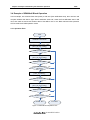
In this example, we will write fixed data (0x5A) to SD card (first 16MB data area), then read out and
compare whether the data is right. When read/write works OK, erase the first 2MB data area in SD
card, then read out and check whether data in first 2MB is zero or not. Both read and write operation
will use multi block DMA operation mode.
3.4.1 Operation Flow
Start
Initialization data buffer
Write data to SD card(first 16MB)
[ em1_sd_multi_write() ]
Write operation OK?
No
Yes
Read data from chip(first 16MB)
[ em1_sd_multi_read() ]
Yes
Read operation OK?
No
Yes
Check data, data right?
[ strncmp() ]
No
Yes
Erase first 2MB in SD card
[ em1_sd_erase() ]
No
Erase operation OK?
Yes
Read data from chip(first 2MB)
[ em1_sd_multi_read() ]
Yes
Read operation OK?
No
Yes
All data is zero?
No
Yes
Normal End
Error End
Figure 3-4 SD Multi block Operation Flow
Application Note S19895EJ1V0AN00
Chapter 3 Example of SD Memory Card Interface Operation
24/52
More details about the functions used in this example please refer to “APPENDIX A SD Driver
Function”
Application Note S19895EJ1V0AN00
Chapter 3 Example of SD Memory Card Interface Operation
25/52
3.4.2 Operation Detail
(1) Initialization Data Buffer
Initialize the write data buffer, set fixed value (0x5A) to write data buffer which will be wrote to SD
card. At the same time, initialize the read data buffer with 0, it will read out data from SD card.
(2) Write Data to SD card
Setting parameters about the data transfer, call the “em1_sd_multi_write()” function to write data
into SD card. Check the write operation, if failed, end the operation and print error information; if
OK, continue the test program.
Details about multiple blocks write operation please refer to “figure2-2 EMMA Mobile 1 SDM
Data Transfer in DMA Mode “.
(3) Read Data from SD Card
Call “em1_sd_multi_read()” function to read out the written data by step (2) from SD card. Check
the read operation, if read failed, end the operation and print error; if read OK, continue the test
program.
Details about multiple blocks read operation please refer to “figure2-2 EMMA Mobile 1 SDM
Data Transfer in DMA Mode “.
(4) Compare Data
Compare the read out data with the written data. If same, print OK; otherwise, print error and end
the test.
(5) Erase first 2MB in SD Card
Call “em1_sd_erase()” function to erase the first 2MB data area in SD card. If failed, end the
operation and print error; if OK, continue the test program.
Details about SD card erase operation please refer to “figure2-3 EMMA Mobile 1 SDM Erase
Operation “.
(6) Read Data from SD Card
Call “em1_sd_multi_read()” function to read out the first 2MB data from SD card. If read failed,
end the operation and print error; if read OK, continue the test program.
(7) Compare Data
Compare the read out data. If 2MB data are all zero, test operation works OK; otherwise, error
end.
Application Note S19895EJ1V0AN00
APPENDIX A SD Driver Function
26/52
APPENDIX A SD Driver Function
A.1 Function List
The following table shows the SD card driver interface functions:
Table A-1 SD Driver Function List
Class
External
function
Internal
function
Function Name
Function Detail
em1_sd_hw_init
em1_sd_init
em1_sd_set_seccnt
em1_sd_send_cmd
em1_sd_set_clk
em1_sd_set_blklength
em1_sd_select_card
em1_sd_set_ext_csd
em1_sd_check_dev_status
em1_sd_erase
em1_sd_single_read
em1_sd_signle_write
em1_sd_multi_read
em1_sd_multi_write
_em1_sd_tranf_prepare
_em1_sd_decode_csd
_em1_sd_check_rsp_status
Init the SDM module setting
SD card initialization
Enable/disable sector and set sector number
Send comand
Set SDM output clock value
Set block length
Select card
Set extend CSD register
Check SD card status
Erase function
Single block read operation in CPU mode
Single block write operation in CPU mode
Multi block read operation in DMA mode
Multi block write operation in DMA mode
Prepare before data transfer
Decode CSD structure
Check response status
A.2 Global Variable Define
Table A-2 Global Variable Define
Name
g_RCA_VAL ushort
Type
Detail
Globle flag for relative address
Application Note S19895EJ1V0AN00
APPENDIX A SD Driver Function
27/52
A.3 Structure & Enum Define
Table A-3 Structure Define
Structure Name
Detail
SDM_NUM
Enum for SDIA, SDIB and SDIC
mmc_csd
CSD register sturcture
A.3.1 mmc_csd
Table A-4 Structure of mmc_csd
Member
Detail
uchar mmca_vsn
ushort cmdclass
ushort tacc_clks
MMC structure version
Command classes
Read access time in clocks
uint tacc_ns
uint max_dtr
uint read_blkbits
uint read_blkbits
uint capacity
uint erase_grp_size
uint erase_grp_mult
uint wp_grp_size
uint read_partial
uint read_misalign
uint write_partial
Read access time in ns
Maximum data transfer speed
Read block bits
Write block bits
Device capacity
Erase group base size
Erase group size multipile factor
Write protect froup size
Whether enable read in partial block
Whether enable read block cross physical block
boundaries
Whether enable write in partial block
uint write_misalign
Whether enable write block cross physical block
boundaries
Application Note S19895EJ1V0AN00
APPENDIX A SD Driver Function
28/52
A.4 Function Details
A.4.1 Hardware Initialization Function
[Function Name]
em1_sd_hw_init
[Format]
int em1_sd_hw_init (SDM_NUM sd_n);
[Argument]
Parameter
Type
sd_n
SDM_NUM
I/O
I
Detail
Enum to select SDIA, SDIB or SDIC
[Function Return]
None
[Flow Chart]
Start
Power on
Clock and Reset setting about
SDM module
Switch GPIO to SD function and
Setting pull-up/pull-down for SD
Wait/Read/Driver ability and Auto
frequency configuration
ASMU_GCLKCTRL4ENA
ASMU_GCLKCTRL4
ASMU_RESETREQ3
ASMU_RESETREQ3ENA
Note1
ASMU_AB1_SDIxWAITCTRL
ASMU_AB1_SDIxREADCTRL
CHG_DRIVE1
ASMU_AUTO_FRQ_MASK3
End
Figure A-1 SDM Hardware Initialization Flow
[Note]
1) Switch GPIO to SD function, users should operate this step according the actual hardware
connection.
Application Note S19895EJ1V0AN00
APPENDIX A SD Driver Function
29/52
A.4.2 Card Init Operation
[Function Name]
em1_sd_init
[Format]
int em1_sd_init(SDM_NUM sd_n ) ;
[Argument]
Parameter
sd_n
Type
SDM_NUM
I/O
I
Detail
Enum to select SDIA, SDIB or SDIC
[Function Return]
DRV_OK
Others: error end
Application Note S19895EJ1V0AN00
APPENDIX A SD Driver Function
30/52
[Flow Chart]
Start
Software reset SD
Setting bus width and response
time out value
Clear and mask all info
Enable and setting clock (in low
frequency)
Send CMD 0, setting SD card into
idle state
Send CMD55 and ACMD41,
setting SD card into ready state
SDIx_SOFT_RST
SDIx_OPTION
Note1
SDIx_INFO1
SDIx_INFO2
SDIx_INFO1_MASK
SDIx_INFO2_MASK
SDIx_CLK_CTRL Note2
SDIx_CMD Note3
SDIx_ARG0
SDIx_ARG1
SDIx_CMD
Get CID info(CMD 2) and setting
relative address(CMD 3) for card
in bus
Get CSD info from card (CMD 9)
Select device (CMD 7)
Setting clock to higher frequency
Note4
Setting transfer bus width and
speed (CMD 6)
Set block size (CMD 16)
End
Figure A-2 SD card Initialization Flow
[Note]
1)Before the initialization of SD card, set the bus width to be 1bit and the response time out value
to be maximum, reason is: in card identification progress, bus width will use 1bit and the clock
frequency should in 10-400 KHz.
2) After setting the clock for SDM transfer, please wait 1ms for stability.
3) After send command, user should check the command response, if error occurred (except
when response time out for CMD 2), the initialization will be ended abnormally.
4) After initialization, users can configure the bus width and clock frequency for transfer speed
according the CSD parameter of SD card, the transfer speed defines in CSD register just clock
frequency not in high speed mode, so the actual transfer speed is related to card specification
version.
Application Note S19895EJ1V0AN00
APPENDIX A SD Driver Function
31/52
A.4.3 Sector Setting
[Function Name]
em1_sd_set_seccnt
[Format]
void em1_sd_set_seccnt(SDM_NUM sd_n ,BOOL bEnable, uint sec_num);
[Argument]
Parameter
Type
I/O
Detail
sd_n
SDM_NUM
I
Enum to select SDIA, SDIB or SDIC
bEnable
BOOL
I
Enable/disable sector
sec_num
uint
I
Sector number
[Function Return]
None
[Flow Chart]
Enable the Sector ?
Yes
Enable and Configure Sector
[ SDIx_STOP
SDIx_SECCNT ]
No
Ensure R/W Operation is Over
[ SDIx_INFO1 ]
Disable Sector
[ SDIx_STOP ]
Figure A-3 Sector Setting Flow
[Note]
None
Application Note S19895EJ1V0AN00
APPENDIX A SD Driver Function
32/52
A.4.4 Send Command
[Function Name]
em1_sd_send_cmd
[Format]
int em1_sd_send_cmd (SDM_NUM sd_n, int cmd) ;
[Argument]
Parameter
Type
I/O
Detail
sd_n
SDM_NUM
I
Enum to select SDIA, SDIB or SDIC
cmd
int
I
Command index that need to be send
[Function Return]
DRV_OK
Others: error end
Application Note S19895EJ1V0AN00
APPENDIX A SD Driver Function
33/52
[Flow Chart]
Start
Clear all information registers
[ SDIx_INFO1
SDIx_INFO2 ]
Enable all errors
[ SDIx_INFO2_MASK ]
Enable response end error
[ SDIx_INFO1 ]
Send command
[ SDIx_CMD ]
Wait until command send end
Yse
Time out?
No
Response end?
[ SDIx_INFO1 ]
Yse
No
No
Error occur?
[ SDIx_INFO2 ]
Yse
Read the error information register
[ SDIx_INFO2 ]
Error occur?
Yse
No
Clear response end information
[ SDIx_INFO1 ]
Clear all error information
[ SDIx_INFO2 ]
Normal End
Error End
Figure A-4 Send Command
[Note]
Send command to SD card.
Application Note S19895EJ1V0AN00
APPENDIX A SD Driver Function
34/52
A.4.5 Set Clock
[Function Name]
em1_sd_set_clk
[Format]
void em1_sd_set_clk(SDM_NUM sd_n, ushort value );
[Argument]
Parameter
Type
I/O
Detail
sd_n
SDM_NUM
I
Enum to select SDIA, SDIB or SDIC
value
ushort
I
Clock setting value
[Function Return]
None
[Flow Chart]
None
[Note]
Set SDIx_CLK_CTRL register.
Application Note S19895EJ1V0AN00
APPENDIX A SD Driver Function
35/52
A.4.6 Set Block Length
[Function Name]
em1_sd_set_blklength
[Format]
int em1_sd_set_blklength(SDM_NUM sd_n, ushort length);
[Argument]
Parameter
Type
I/O
Detail
sd_n
SDM_NUM
I
Enum to select SDIA, SDIB or SDIC
length
ushort
I
Block length setting value
[Function Return]
DRV_OK
Others: error end
[Flow Chart]
Start
Command parameter setting
[ SDIx_ARG0 SDIx_ARG1 ]
Send CMD16 to set block length
[ em1_sd_send_cmd() ]
Send command OK?
No
Yse
Set block size
[ SDIx_SIZE ]
Normal End
Error End
Figure A-5 Set Block Length
[Note]
Data transfer block length setting.
Application Note S19895EJ1V0AN00
APPENDIX A SD Driver Function
36/52
A.4.7 Select Card
[Function Name]
em1_sd_select_card
[Format]
int em1_sd_select_card(SDM_NUM sd_n, uint RCA);
[Argument]
Parameter
Type
I/O
Detail
sd_n
SDM_NUM
I
Enum to select SDIA, SDIB or SDIC
RCA
uint
I
Relative card address that need to be select
[Function Return]
DRV_OK
Others: error end
[Flow Chart]
Start
Setting RCA for command
parameters
[ SDIx_ARG0 SDIx_ARG1 ]
Send CMD7 to select card
[ em1_sd_send_cmd() ]
Send command OK?
No
Yse
Normal End
Error End
Figure A-6 Select Card
[Note]
None.
Application Note S19895EJ1V0AN00
APPENDIX A SD Driver Function
37/52
A.4.8 Check Device Status
[Function Name]
em1_sd_check_dev_status
[Format]
int em1_sd_check_dev_status (SDM_NUM sd_n) ;
[Argument]
Parameter
sd_n
Type
SDM_NUM
I/O
I
Detail
Enum to select SDIA, SDIB or SDIC
[Function Return]
DRV_DEV_LOCKED
DRV_DEV_UNLOCKED
DRV_ERR_STATE
[Flow Chart]
Application Note S19895EJ1V0AN00
APPENDIX A SD Driver Function
38/52
Start
Set command parameters(RCA)
[ SDIx_ARG0 SDIx_ARG1 ]
Send CMD13 to get card status
[ em1_sd_send_cmd() ]
Send command OK?
No
Yse
Read response value
[ SDIx_RSP0 and SDIx_RSP1 ]
Check whether card locked
Check whether error occur
Error occured?
Yse
No
Normal End
Error End
Figure A-7 Check Card Stauts
[Note]
Check card status register.
Application Note S19895EJ1V0AN00
APPENDIX A SD Driver Function
39/52
A.4.9 Erase Function
[Function Name]
em1_sd_erase
[Format]
int em1_sd_erase(SDM_NUM sd_n, uint str_addr, uint end_addr) ;
[Argument]
Parameter
Type
I/O
Detail
sd_n
SDM_NUM
I
Enum to select SDIA, SDIB or
SDIC
str_addr
uint
I
Start erase group unit address
end_addr
uint
I
End of erase group unit address
[Function Return]
DRV_OK
Others: error end
[Flow Chart]
Please refer to “figure2-3 EMMA Mobile 1 SDM Erase Operation” in “chapter 2.3 Erase”.
[Note]
None
Application Note S19895EJ1V0AN00
APPENDIX A SD Driver Function
40/52
A.4.10 Single Block Read
[Function Name]
em1_sd_single_read
[Format]
int em1_sd_single_read(SDM_NUM sd_n, uint address, uchar *data );
[Argument]
Parameter
Type
I/O
Detail
sd_n
SDM_NUM
I
Enum to select SDIA, SDIB or SDIC
address
uint
I
block address to be read
data
uchar *
I/O
read out data buffer
[Function Return]
DRV_OK
Others: error end
Application Note S19895EJ1V0AN00
APPENDIX A SD Driver Function
41/52
[Flow Chart]
Start
Check parameter
[ whether data buffer is NULL ]
Wait for SDM not busy
[ SDIx_INFO2[14] ]
Set sector enable and sector
number to be 1
SDIx_STOP
SDIx_SECCNT
Transfer prepare
[ _em1_sd_transfer_prepare ]
Send single block read command
[ em1_sd_send_cmd() ]
No
Send command Ok?
Yes
Wait for read enable
[ SDIx_INFO2]
No
Check response OK?
[ _em1_sd_check_rsp_status]
Yes
Read data
[ SDIx_BUF0 ]
No
R/W transfer end?
Yes
Clear response and r/w end info
[ SDIx_INFO1 ]
Error occur?
[ SDIx_INFO2 ]
Check device status
[ em1_sd_check_dev_status()]
Yes
Clear all error info
[ SDIx_INFO2 ]
Error occur?
Yes
No
Normal End
Error End
Figure A-8 Single Block Read in CPU mode
[Note]
None
Application Note S19895EJ1V0AN00
No
APPENDIX A SD Driver Function
42/52
A.4.11 Single Block Write
[Function Name]
em1_sd_single_write
[Format]
int em1_sd_single_write(SDM_NUM sd_n, uint address, uchar *data );
[Argument]
Parameter
Type
I/O
Detail
sd_n
SDM_NUM
I
Enum to select SDIA, SDIB or SDIC
address
uint
I
block address to be write
data
uchar *
I/O
Write source data buffer
[Function Return]
DRV_OK
Others: error end
Application Note S19895EJ1V0AN00
APPENDIX A SD Driver Function
43/52
[Flow Chart]
Start
Check parameter
[ whether data buffer is NULL ]
Wait for SDM not busy
[ SDIx_INFO2[14] ]
Set sector enable and sector
SDIx_STOP
SDIx_SECCNT
number to be 1
Transfer prepare
[ _em1_sd_transfer_prepare() ]
Send single block write command
[ em1_sd_send_cmd() ]
No
Send command Ok?
Yes
Wait for write enable
[ SDIx_INFO2]
No
Check response OK?
[ _em1_sd_check_rsp_status]
Yes
Write data
[ SDIx_BUF0 ]
Note1
No
R/W transfer end?
Yes
Clear response and r/w end info
[ SDIx_INFO1 ]
Error occur?
[ SDIx_INFO2 ]
Check device status
[ em1_sd_check_dev_status()]
Yes
Clear all error info
[ SDIx_INFO2 ]
Error occur?
No
Yes
No
Normal End
Error End
Figure A-9 Single Block Write in CPU mode
[Note]
1) During write operation, check SDIx_INFO2, if buffer write access error occur, end the write
operation and return with error information.
Application Note S19895EJ1V0AN00
APPENDIX A SD Driver Function
44/52
A.4.12 Multiple Block Read
[Function Name]
em1_sd_multi_read
[Format]
int em1_sd_multi_read (SDM_NUM sd_n, uint address, uchar *read_buf, uint blk_num);
[Argument]
Parameter
Type
I/O
Detail
sd_n
SDM_NUM
I
Enum to select SDIA, SDIB or SDIC
address
uint
I
block address to be read
read_buf
uchar *
blk_num
uint
I/O
I
read out data buffer
block number to be read
[Function Return]
DRV_OK
Others: error end
[Flow Chart]
Please refer to “figure2-2 EMMA Mobile 1 SDM Data Transfer in DMA Mode” in “chapter 2.2
Data Transfer”.
[Note]
None.
Application Note S19895EJ1V0AN00
APPENDIX A SD Driver Function
45/52
A.4.13 Multiple Block Write
[Function Name]
em1_sd_multi_write
[Format]
int em1_sd_multi_write (SDM_NUM sd_n, uint address, uchar * write_buf, uint blk_num);
[Argument]
Parameter
Type
I/O
Detail
sd_n
SDM_NUM
I
Enum to select SDIA, SDIB or SDIC
address
uint
I
block address to be write
write_buf
uchar *
blk_num
uint
I/O
write source data buffer
I
block number to be write
[Function Return]
DRV_OK
Others: error end
[Flow Chart]
Please refer to “figure2-2 EMMA Mobile 1 SDM Data Transfer in DMA Mode” in “chapter 2.2
Data Transfer”.
[Note]
None.
Application Note S19895EJ1V0AN00
APPENDIX A SD Driver Function
46/52
A.4.14 Transfer Prepare
[Function Name]
_em1_sd_transfer_prepare
[Format]
int _em1_sd_transfer_prepare(SDM_NUM sd_n);
[Argument]
Parameter
sd_n
Type
SDM_NUM
I/O
I
Detail
Enum to select SDIA, SDIB or SDIC
[Function Return]
None
[Flow Chart]
Start
All information clear
[ SDIx_INFO1 SDIx_INFO2 ]
Clear stop setting bit
[ SDIx_STOP ]
Enable all error occur
[ SDIx_INFO2_MASK ]
Enable R/W access end
[ SDIx_INFO1_MASK ]
End
Figure A-10 Register Prepare before Data transfer
[Note]
None.
Application Note S19895EJ1V0AN00
APPENDIX A SD Driver Function
47/52
A.4.15 Decode CSD
[Function Name]
_em1_sd_decode_csd
[Format]
void _em1_sd_decode_csd(uint *raw_csd);
[Argument]
Parameter
raw_csd
Type
uint
I/O
I
Detail
Raw CSD value buffer
[Function Return]
None
[Flow Chart]
None
[Note]
This function will decode the response of SEND_CSD command; get CSD members that
useful for data transfer.
Application Note S19895EJ1V0AN00
APPENDIX A SD Driver Function
48/52
A.4.16 Check Response Status
[Function Name]
_em1_sd_check_rsp_status
[Format]
int _em1_sd_check_rsp_status(SDM_NUM sd_n);
[Argument]
Parameter
sd_n
Type
I/O
SDM_NUM
I
Detail
Enum to select SDIA, SDIB or SDIC
[Function Return]
DRV_OK
DRV_ERR_STATE
[Flow Chart]
Start
Read response value
[ SDIx_RSP0 and SDIx_RSP1 ]
Check whether error occur
Error occured?
Yse
No
Normal End
Error End
Figure A-11 Check Response Status
[Note]
None
Application Note S19895EJ1V0AN00
APPENDIX B COMMANDS
49/52
APPENDIX B COMMANDS
Following table shows the simple function of the SD card command which used in this document.
More details about the commands format and function please refer to SD card user’s manual.
Table B-1 Command Description List
CMD
INDEX
Argument
CMD0
CMD1
[31:0] stuff bits
CMD2
[31:0] stuff bits
CMD3
[31:16] RCA
[15:0] stuff bits
Abbreviation
Command Description
GO_IDLE_STATE Resets the card to idle state
Reserved
Ask card to send their CID number on the
ALL_SEND_CID
CMD line
SET_RELATIVE_A
Assigns relative address to the card
DDR
CMD4
Not Supported
CMD5
Reserved
CMD6
[31] Mode
0: Check
1: Switch
[30:24] (all 0)
[23:20]: group 6
[19:16]: group 5
[15:12]: group 4
[11:8]: group 3
[7:4] : group 2 for
command
[3:0]: group 1for
access mode
SWITCH
CMD7
[31:16] RCA
[15:0] stuff bits
SELECT/DESELEC
T_CARD
CMD8
CMD9
CMD10
[31:16] RCA
[15:0] stuff bits
[31:16] RCA
[15:0] stuff bits
CMD11
[31:0] data
address1
CMD12
[31:0] stuff bits
CMD13
[31:16] RCA
[15:0] stuff bits
Checks switchable function (mode 0) and
switch card function (mode 1).
Select device by its own relative address
and gets deselected by any other address;
address 0 deselects the card.
Reserved
Addressed card sends its Card-Specific
SEND_CSD
Data (CSD) on the CMD line.
Addressed card sends its Card Identification
SEND_CID
(CID) on CMD the line.
Reads data stream from the card, starting at
READ_DAT_UNTIL
the
given
address,
until
a
_STOP
STOP_TRANSMISSION follows
STOP_TRANSMIS
Forces the card to stop transmission
SION
SEND_STATUS
Addressed card sends its status register.
Application Note S19895EJ1V0AN00
APPENDIX B COMMANDS
CMD14
CMD15
CMD16
CMD17
CMD18
[31:16] RCA
[15:0] stuff bits
[31:0] block
length
[31:0] data
address
[31:0] data
address
50/52
Reserved
GO_INACTIVE_ST
Sets card to inactive state
ATE
Sets the block length (in bytes) for all
SET_BLOCKLEN
following block commands (read and write).
READ_SINGLE_BL Reads a block of the size selected by the
OCK
SET_BLOCKLEN command
READ_MULTIPLE_
Multipile block read command
BLOCK
CMD19
~
CMD23
Reserved
CMD24
[31:0] data
address
CMD25
[31:0] data
address
CMD26
CMD27
CMD28
CMD29
CMD30
[31:0] stuff bits
[31:0] data
address
[31:0] data
address
[31:0] write
protect data
address
CMD31
CMD32
[31:0] data
address
CMD33
[31:0] data
address
CMD34
~
CMD37
CMD38
Writes a block of the size selected by the
SET_BLOCKLEN command.
Continuously writes blocks of data until a
WRITE_MULTIPLE
STOP_TRANSMISSION follows or the
_BLOCK
requested number of block received
Not applicable
Programming of the programmable bits of
PROGRAM_CSD
the CSD
Sets the write protection bit of the addressed
SET_WRITE_PROT
group.
CLR_WRITE_PRO Clears the write protection bit of the
T
addressed group
WRITE_BLOCK
SEND_WRITE_PR
OT
Asks card to send the status of the write
protection bits.
Reserved
ERASE_GROUP_S Sets the address of the first erase group
TART
within a range to be selected for erase
Sets the address of the last erase group
ERASE_GROUP_E
within a continuous range to be selected for
ND
erase
Reserved
[31:0] stuff bits
ERASE
Erases all previously selected write blocks
CMD39
~
CMD41
Reserved
CMD42
~
CMD54
Reserved
CMD55
[31:16] RCA
[15:0] stuff bits
APP_CMD
CMD56
[31:1] stuff bits.
GEN_CMD
Indicates to the card that the next command
is an application specific command rather
than a standard command
Used either to transfer a data block to the
Application Note S19895EJ1V0AN00
APPENDIX B COMMANDS
51/52
[0]: RD/ WR1
card or to get a data block from the card for
general purpose / application specific
commands.
CMD57
…
CMD63
ACMD
6
ACMD
13
ACMD
17 ~21
Reserved
[31:2] stuff bits
[1:0]bus width
[31:0] stuff bits
SET_BUS_WIDTH
SD_STATUS
Defines the data bus width (’00’=1bit
or ’10’=4 bits bus) to be used for data
transfer.
Send the SD Card status
Reserved
ACMD
22
[31:0] stuff bits
SEND_NUM_WR_B
LOCKS
ACMD
23
[31:23] stuff bits
[22:0]Number of
blocks
SET_WR_BLK_ER
ASE_COUNT
ACMD
25~40
Send the number of the written (without
errors) write blocks. Responds with
32bit+CRC data block.
Set the number of write blocks to be preerased before writing (to be used for faster
Multiple Block WR command). “1”=default
(one wr block)2.
Reserved
ACMD
41
[31:0]OCR
without busy
SD_APP_OP_CON
D
ACMD
42
ACMD
43~49
ACMD
51
[31:1] stuff bits
[0]set_cd
SET_CLR_CARD_
DETECT
Asks the accessed card to send its operating
condition register (OCR) con tent in the
response on the CMD line.
Connect[1]/Disconnect[0] the 50KOhm pullup resistor on CD/DAT3 (pin 1) of the card
Reserved
[31:0] stuff bits
SEND_SCR
Reads the SD Configuration Register (SCR).
Application Note S19895EJ1V0AN00
ANNEX Modification History
52/52
ANNEX Modification History
Number
Ver 1.00
Modification Contents
Author
New version
Application Note S19895EJ1V0AN00
Date
Aug.4.2009