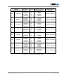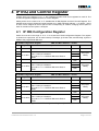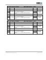
1
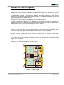
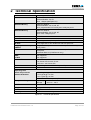
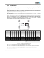
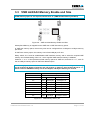
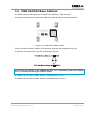
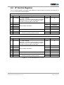
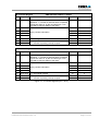
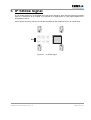
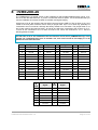
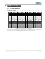
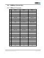
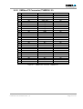
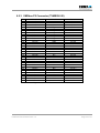
The Embedded I/O Company TVME200 4 Slot IndustryPack® VMEbus Carrier Version 1.1 User Manual Issue 1.5 November 2004 TEWS TECHNOLOGIES GmbH Am Bahnhof 7 Phone: +49-(0)4101-4058-0 e-mail: [email protected] 25469 Halstenbek / Germany Fax: +49-(0)4101-4058-19 www.tews.com TEWS TECHNOLOGIES LLC 1 E. Liberty Street, Sixth Floor Phone: +1 (775) 686 6077 e-mail: [email protected] Reno, Nevada 89504 / USA Fax: +1 (775) 686 6024 www.tews.com TVME200-10 4 Slot IndustryPack VMEbus Carrier with front I/O TVME200-20 4 Slot IndustryPack VMEbus Carrier with Front I/O and additional Rear I/O of ‘IP C’ and ‘IP D’ via VME P2 This document contains information, which is proprietary to TEWS TECHNOLOGIES GmbH. Any reproduction without written permission is forbidden. TEWS TECHNOLOGIES GmbH has made any effort to ensure that this manual is accurate and complete. However TEWS TECHNOLOGIES GmbH reserves the right to change the product described in this document at any time without notice. TEWS TECHNOLOGIES GmbH is not liable for any damage arising out of the application or use of the device described herein. Style Conventions Hexadecimal characters are specified with prefix 0x, i.e. 0x029E (that means hexadecimal value 029E). For signals on hardware products, an ‚Active Low’ is represented by the signal name with # following, i.e. IP_RESET#. Access terms are described as: W Write Only R Read Only R/W Read/Write R/C Read/Clear R/S Read/Set 2001-2004 by TEWS TECHNOLOGIES GmbH IndustryPack is a registered trademark of SBS Technologies, Inc Issue Description Date 1.0 First Issue November 2001 1.1 Value correction chapter “VMEbus P1 connector” and general revision 1.2 Module TVME200-20 added October 2002 December 2003 1.3 Correction “VMEbus P2 Connector” (TVME200-10) December 2003 1.4 Function added to switch S3 September 2004 1.5 Clarification of Interrupt Mapping November 2004 TVME200 User Manual Issue 1.5 Page 2 of 25 Table of Contents 1 2 3 PRODUCT DESCRIPTION ......................................................................................... 5 TECHNICAL SPECIFICATION................................................................................... 6 CONFIGURATION...................................................................................................... 7 3.1 3.2 3.3 3.4 4 VME A16 Base Address..................................................................................................................8 Interrupts .......................................................................................................................................10 VME A24/A32 Memory Enable and Size......................................................................................11 VME A24/A32 Base Address ........................................................................................................12 IP IRQ AND CONTROL REGISTER......................................................................... 14 4.1 IP IRQ Configuration Register .....................................................................................................14 4.2 IP Control Register........................................................................................................................16 5 6 7 IP STROBE SIGNAL ................................................................................................ 18 INSTALLATION OF INDUSTRYPACKS .................................................................. 19 FRONT PANEL INDICATORS ................................................................................. 20 7.1 ACK and Power LEDs ...................................................................................................................20 7.2 Fuses and Filters...........................................................................................................................20 8 9 TVME200-20 ............................................................................................................. 21 PIN ASSIGNMENT ................................................................................................... 22 9.1 IP Connectors................................................................................................................................22 9.2 VMEbus Connectors .....................................................................................................................23 9.2.1 VMEbus P1 Connector .......................................................................................................23 9.2.2 VMEbus P2 Connector (TVME200-10) ..............................................................................24 9.2.3 VMEbus P2 Connector (TVME200-20) ..............................................................................25 TVME200 User Manual Issue 1.5 Page 3 of 25 Table of Figures FIGURE 1-1 : BLOCK DIAGRAM......................................................................................................................5 FIGURE 2-1 : TECHNICAL SPECIFICATION...................................................................................................6 FIGURE 3-1 : ROTARY SWITCH S1 – S6........................................................................................................7 FIGURE 3-2 : CONFIGURATION STEPS.........................................................................................................7 FIGURE 3-3 : VME A16 BASE ADDRESS .......................................................................................................8 FIGURE 3-4 : VME A16 ADDRESS MAP (S3 = “0” TO “7”) .............................................................................9 FIGURE 3-5 : VME A16 ADDRESS MAP (S3 = “8” TO “F”) .............................................................................9 FIGURE 3-6 : INTERRUPT MAPPING ...........................................................................................................10 FIGURE 3-7 : VME INTERRUPT MAPPING BY S3 .......................................................................................10 FIGURE 3-8 : VME A24/A32 MEMORY ENABLE AND SIZE.........................................................................11 FIGURE 3-9 : VME MEMORY SIZE BY S4 ....................................................................................................11 FIGURE 3-10: VME A24/A32 BASE ADDRESS .............................................................................................12 FIGURE 3-11: VME A24/A32 ADDRESS MAP...............................................................................................13 FIGURE 4-1 : IP IRQ CONFIGURATION REGISTERS (IP A / IP B)..............................................................14 FIGURE 4-2 : IP IRQ CONFIGURATION REGISTERS (IP C / IP D) .............................................................15 FIGURE 4-3 : IP CONTROL REGISTERS (IP A / IP B)..................................................................................16 FIGURE 4-4 : IP CONTROL REGISTERS (IP C / IP D) .................................................................................17 FIGURE 5-1 : IP STROBE SIGNAL ................................................................................................................18 FIGURE 6-1 : FRONT PANEL.........................................................................................................................19 FIGURE 7-1 : IP ACK LED ..............................................................................................................................20 FIGURE 7-2 : IP POWER LED........................................................................................................................20 FIGURE 8-1 : J3 PIN ASSIGNMENT ..............................................................................................................21 FIGURE 8-2 : J4 AND J5 PIN ASSIGNMENT.................................................................................................21 FIGURE 9-1 : IP J1 LOGIC INTERFACE PIN ASSIGNMENT........................................................................22 FIGURE 9-2 : VMEBUS P1 CONNECTOR.....................................................................................................23 FIGURE 9-3 : VMEBUS P2 CONNECTOR TVME200-10 ..............................................................................24 FIGURE 9-4 : VMEBUS P2 CONNECTOR TVME200-20 ..............................................................................25 TVME200 User Manual Issue 1.5 Page 4 of 25 1 Product Description The TVME200 is a 6U VMEbus Carrier for up to 4 single-size or two double-size IndustryPack (IP) modules used to build modular, flexible and cost effective I/O solutions for applications in process control, medical systems, telecommunication and traffic control. The TVME200 is designed in accordance to VMEbus Specification ANSI/VITA 1-1994 and the IndustryPack Logic Interface Specification ANSI/VITA 4-1995. It guarantees compatibility with the wide range of IndustryPacks in a VMEbus system. IndustryPack I/O and ID spaces are mapped into the VME A16/D16 space. IP Memory spaces are mapped into the VME A24 or A32 space. D08 and D16 accesses are supported. If mapped in the VME A24 space, the size of the required memory space is configurable. In VME A32 space, there is a fixed space of 8 Mbyte for each IP module. Strobe signals of all IP modules are accessible via a 4 pin jumper block on the TVME200. DMA, 32 bit access and 32 MHz operations are not supported. Four 50 pin, 0.1 inch flat ribbon cable connectors mounted in the front panel of the TVME200 provide access to all IP I/O lines. Status indicators for IP access, +5V and +/-12V are provided. A set of 16-position rotary switches allows easy configuration of VME Short I/O and Memory addresses. Interrupt routing from the IP slots to the VME IRQ’s can be done in two ways: programmable by software or selection of predefined sets by a rotary switch. The IP power lines are fuse protected by self healing fuses and RF filtered. The operating temperature range is -40°C and +85°C. Additional on the TVME200-20 all I/O lines of ‘IP D’ are routed to VME P2 and 14 user selectable I/O lines of ‘IP C’ can be routed to VME P2 via a jumper field. Figure 1-1 : Block Diagram TVME200 User Manual Issue 1.5 Page 5 of 25 2 Technical Specification VMEbus Slave Interface According to VMEbus specification, ANSI / VITA 1-1994, 6U Board Short I/O VME A16, D08/16, Address Modifier: 29, 2D Size: 1 Kbytes (256 Bytes / IP) Standard Memory VME A24, D08/16, Address Modifier: 39, 3A, 3D, 3E Size: programmable from 32 Kbytes to 2 Mbytes per IP Extended Memory VME A32, D08/16, Address Modifier: 09, 0A, 0D, 0E Size: fixed, 8 Mbytes per IP Interrupts VME IRQ1-7 IP Interface According to IndustryPack specification ANSI / VITA 4-1995 IP Slots Four single size or two double size with front panel I/O Mapping of IP Interrupts to VMEbus Programmable by software or selection of predefined sets by a rotary switch I/O access 50 pin 0.1 inch flat ribbon cable connector per IP, mounted in the front panel Additional Rear I/O (TVME200-20 only) DMA 32 MHz Not supported Not supported Status LEDs ACK LED for each IP slot +5V Power LED for each IP slot +12V and –12V Power LED Protection Self healing fuses and RF-filtering on all IP power lines Operating Data Power Requirements without IP Modules 300 mA typical @+ 5 VDC 1 mA typical @+ 12 VDC 1 mA typical @ -12 VDC Additional Power is required by IP modules Temperature Range Operating Storage – 40°C to + 85C – 40°C to + 125°C MTBF 366000 h Weight 260 g – no IndustryPack inserted Size Singe Size 6U Euro Card Humidity 5 – 95 % non-condensing Figure 2-1 : Technical Specification TVME200 User Manual Issue 1.5 Page 6 of 25 3 Configuration Setting 6 rotary switches allows all required configuration of the TVME200. Position of the switches is shown below: Figure 3-1 : Rotary Switch S1 – S6 Step Rotary Switch Function Default Value 1 S1 / S2 VME A16 Base Address 0x6000 2 S3 Interrupt Mapping VIPC6xx compatible 3 S4 VME A24/A32 Memory Enable and Memory Size Disabled 4 S5 / S6 VME A24/A32 Memory Base Address A24: 0xD00000 A32: 0xD0000000 Figure 3-2 : Configuration Steps TVME200 User Manual Issue 1.5 Page 7 of 25 3.1 VME A16 Base Address The VME A16 Base Address of the TVME200 is set by rotary switch S1 and S2. Rotary switch S1 sets A[15:12] of the VME A16 Base Address. Rotary switch S2 sets A[11:10] of the VME A16 Base Address. Figure 3-3 : VME A16 Base Address The default value for the VME A16 Base Address is 0x6000 (S1=6, S2=0). The TVME200 requires an address space of 1 Kbytes within the VME A16 address space. Each of the four IP slots occupies 256 bytes within this 1 Kbytes VME A16 address space. The address space for each IP is divided into the following areas: IP I/O space, IP ID space and the IP IRQ and Control Register. The IP I/O space has a size of 128 bytes. The size of the IP ID space and the IP IRQ and Control Register depends on the position of switch S3: With S3 = “0” to “7”, the IP IRQ and Control Registers of the TVME200 are accessible, and the size of the IP ID space is 64 bytes. The remaining 64 bytes are occupied by the IP IRQ and Control Registers. If switch S3 = “8” to “F”, the IP IRQ and Control Registers of the TVME200 are not accessible, and the corresponding address range is added to the IP ID space, resulting in a size of 128 bytes for the IP ID space with S3 = “8” to “F”. This configuration is necessary for IP modules that require access to the ID Space above the ID PROM. See figures below for more details. TVME200 User Manual Issue 1.5 Page 8 of 25 VME A16 Base Address Description Default + 0x0000 I/O Space IP A 0x6000 + 0x0080 ID Space IP A 0x6080 + 0x00C0 IRQ and Control Register IP A 0x60C0 + 0x0100 I/O Space IP B 0x6100 + 0x0180 ID Space IP B 0x6180 + 0x01C0 IRQ and Control Register IP B 0x61C0 + 0x0200 I/O Space IP C 0x6200 + 0x0280 ID Space IP C 0x6280 + 0x02C0 IRQ and Control Register IP C 0x62C0 + 0x0300 I/O Space IP D 0x6300 + 0x0380 ID Space IP D 0x6380 + 0x03C0 IRQ and Control Register IP D 0x63C0 Figure 3-4 : VME A16 Address Map (S3 = “0” to “7”) VME A16 Base Address Description Default + 0x0000 I/O Space IP A 0x6000 + 0x0080 ID Space IP A 0x6080 + 0x0100 I/O Space IP B 0x6100 + 0x0180 ID Space IP B 0x6180 + 0x0200 I/O Space IP C 0x6200 + 0x0280 ID Space IP C 0x6280 + 0x0300 I/O Space IP D 0x6300 + 0x0380 ID Space IP D 0x6380 Figure 3-5 : VME A16 Address Map (S3 = “8” to “F”) TVME200 User Manual Issue 1.5 Page 9 of 25 3.2 Interrupts Each IndustryPack can generate interrupts on two interrupt request lines (INT0 and INT1). The VMEbus offers seven interrupt request level. IRQ7 has the highest priority, IRQ1 has the lowest priority. IP interrupt requests can be mapped to any of the 7 VME interrupt request levels. Interrupt routing from the IP slots to the VME IRQs can be done by selection of predefined sets with a rotary switch or programmable by software if S3 is in the range of “0” to “7”. For more information about fully programmable interrupt mapping please refer to chapter “IP IRQ and Control Register”. Rotary switch S3 can be used to select predefined sets of mapping of the eight IP interrupt request (two requests per IP slot) to the seven VME interrupt request level. The mapping selected with S3 = “0” to “7” is mirrored at S3 = “8” to “F”. The difference is that access to the IP IRQ and Control Registers of the TVME200 is only possible in switch position S3 = “0” to “7”. See chapter “IP IRQ and Control Register” and chapter “VME A16 Base Address” for more details. Figure 3-6 : Interrupt Mapping S3 = 0 1 2 3 4 5…7 8* 9* A* B* C* D*…F* IP A, Int0 - 1 4 6 1 reserved - 1 4 6 1 reserved IP A, Int1 - 2 5 4 1 reserved - 2 5 4 1 reserved IP B, Int0 - 3 2 3 2 reserved - 3 2 3 2 reserved IP B, Int1 - 4 1 1 2 reserved - 4 1 1 2 reserved IP C, Int0 - 5 4 6 3 reserved - 5 4 6 3 reserved IP C, Int1 - 6 5 4 3 reserved - 6 5 4 3 reserved IP D, Int0 - 7 2 3 4 reserved - 7 2 3 4 reserved IP D, Int1 - - 1 1 4 reserved - - 1 1 4 reserved “-” = No VME IRQ level mapped to IP INTx * no access to the IP IRQ and Control registers of the TVME200 , see Chapter 4 and Chapter 3.1 for more details. Figure 3-7 : VME Interrupt Mapping by S3 S3 = “1”, “9” corresponds to the VME Interrupt Mapping of the VIPC6xx. S3 = “2”, “A” corresponds to the VME Interrupt Mapping of the VIPC610-01 (equal to two VIPC310). S3 = “3”, “B” corresponds to the VME Interrupt Mapping of another version of the VIPC310. The default value for S3 is “1”. TVME200 User Manual Issue 1.5 Page 10 of 25 3.3 VME A24/A32 Memory Enable and Size If VME memory space is not required, switch S4 to “0” (VME A24/A32 memory disabled). Figure 3-8 : VME A24/A32 Memory Enable and Size IndustryPack Memory is mapped into the VME A24 or VME A32 memory space. In VME A24 memory space, the memory size can be configured from 32 Kbytes to 2 Mbyte memory per IP slot. In VME A32 memory space, the memory size is fixed 8 Mbyte per IP slot. Rotary switch S4 is used to enable/disable VME A24/A32 memory and to select the required VME memory size. Default setting of S4 is “0”, which signifies VME A24/A32 memory is disabled. Positions “1” to “7” of S4 represent several memory spaces in VME A24, and with S4 = “F”, each IP has an 8 Mbyte memory space in VME A32 address space. The Memory Spaces for all IPs have the same size. If i.e. one IP requires 128 Kbytes of memory, one IP requires 64 Kbytes of memory and 2 IP require no memory, then S4 must be set to “3”, which selects a VME A24 memory size of 512 Kbytes, 128 Kbytes memory for each IP. Value of S4: VME Memory Size: 0x0 VME A24/A32 memory disabled 0x1 A24 128 Kbytes 0x2 A24 256 Kbytes 64 Kbytes / IP 0x3 A24 512 Kbytes 128 Kbytes / IP 0x4 A24 1 Mbytes 256 Kbytes / IP 0x5 A24 2 Mbyte 512 Kbytes / IP 0x6 A24 4 Mbyte 1 Mbyte / IP 0x7 A24 8 Mbyte 2 Mbyte / IP 0x8 – 0xE 0xF 32 Kbytes / IP reserved A32 32 Mbyte 8 Mbyte / IP Slot Figure 3-9 : VME Memory Size by S4 TVME200 User Manual Issue 1.5 Page 11 of 25 3.4 VME A24/A32 Base Address The memory space of IndustryPacks is mapped in the VME A24 or VME A32 space. The memory base address for VME A24 or VME A32 is both set with the switches S5 and S6. Figure 3-10: VME A24/A32 Base Address If memory space is located in VME A24, S5 represents A[23:20], and S6 represents A[19:16]. In VME A32, S5 represents [A31:28] and S6 represents A[27:24]. The memory base address of the TVME200 must be set on a boundary, equal to the memory size, as selected by S4! See figure below for details. The default value for VME A24 base address is 0xD00000 (S5=D, S6=0). The default value for VME A32 base address is 0xD0000000 (S5=D, S6=0). TVME200 User Manual Issue 1.5 Page 12 of 25 IP Memory Size IP Slot IP Memory Location: Mem. Base Address + VMEbus Address Boundary 128 Kbytes 32 Kbytes 32 Kbytes 32 Kbytes 32 Kbytes A B C D 0x000000 0x008000 0x010000 0x018000 multiple of 0x020000 256 Kbytes 64 Kbytes 64 Kbytes 64 Kbytes 64 Kbytes A B C D 0x000000 0x010000 0x020000 0x030000 multiple of 0x040000 512 Kbytes 128 Kbytes 128 Kbytes 128 Kbytes 128 Kbytes A B C D 0x000000 0x020000 0x040000 0x060000 multiple of 0x080000 1 Mbytes 256 Kbytes 256 Kbytes 256 Kbytes 256 Kbytes A B C D 0x000000 0x040000 0x080000 0x0C0000 multiple of 0x100000 2 Mbytes 512 Kbytes 512 Kbytes 512 Kbytes 512 Kbytes A B C D 0x000000 0x080000 0x100000 0x180000 multiple of 0x200000 4 Mbytes 1 Mbytes 1 Mbytes 1 Mbytes 1 Mbytes A B C D 0x000000 0x100000 0x200000 0x300000 multiple of 0x400000 8 Mbytes 2 Mbytes 2 Mbytes 2 Mbytes 2 Mbytes A B C D 0x000000 0x200000 0x400000 0x600000 multiple of 0x800000 32 Mbytes 8 Mbytes 8 Mbytes 8 Mbytes 8 Mbytes A B C D 0x00000000 0x00800000 0x01000000 0x01800000 multiple of 0x02000000 TVME200 VME A24/A32 Size A24 A24 A24 A24 A24 A24 A24 A32 Figure 3-11: VME A24/A32 Address Map TVME200 User Manual Issue 1.5 Page 13 of 25 4 IP IRQ and Control Register If switch S3 is in the range of “0” to “7”, the TVME200 provides a set of two registers for each IP: The IP IRQ Configuration Register and the IP Control Register. Setting switch S3 to a value of “8” to “F” disables the IP IRQ Register and the IP Control Register. The address range of the IP IRQ and Control Register from “VME A16 Base Address” + “IP Offset” + 0xC0 to 0xFF is then mapped to the ID Space of the corresponding IP module, enlarging the ID Space of each IP module from 64 bytes to 128 bytes. 4.1 IP IRQ Configuration Register Switch S3 must be in the range of “0” to “7” to access the IP IRQ Configuration Register. The register is divided in 2 equal parts, one for each interrupt. The bits[0, 4] are the LSBs, and the bits[2, 6] are the MSBs of the programmed IRQ level. IP A IRQ Configuration Register Bit Symbol VME A16 Base Address + 0x00C1 Description Access Reset Value R/W Depends on S3 jumper setting 7 6 5 IP A, INT1 4 VME IRQ Level 000 = interrupt is disabled [6:4] 001 to 111 = VMEbus IRQ levels IRQ1 to IRQ7 3 IP A, INT0 0 VME IRQ Level 000 = interrupt is disabled [2:0] 001 to 111 = VMEbus IRQ levels IRQ1 to IRQ7 IP B IRQ Configuration Register Bit R/W R/W 2 1 R/W Symbol R/W R/W R/W Depends on S3 jumper setting VME A16 Base Address + 0x01C1 Description Access Reset Value R/W Depends on S3 jumper setting 7 6 5 IP B, INT1 4 VME IRQ Level 000 = interrupt is disabled [6:4] 001 to 111 = VMEbus IRQ levels IRQ1 to IRQ7 3 0 R/W R/W 2 1 R/W IP B, INT0 VME IRQ Level 000 = interrupt is disabled [2:0] 001 to 111 = VMEbus IRQ levels IRQ1 to IRQ7 R/W R/W R/W Depends on S3 jumper setting Figure 4-1 : IP IRQ Configuration Registers (IP A / IP B) TVME200 User Manual Issue 1.5 Page 14 of 25 IP C IRQ Configuration Register Bit Symbol VME A16 Base Address + 0x02C1 Description Access Reset Value R/W Depends on S3 jumper setting 7 6 5 IP C, INT1 4 VME IRQ Level 000 = interrupt is disabled [6:4] 001 to 111 = VMEbus IRQ levels IRQ1 to IRQ7 3 IP C, INT0 0 VME IRQ Level 000 = interrupt is disabled [2:0] 001 to 111 = VMEbus IRQ levels IRQ1 to IRQ7 IP D IRQ Configuration Register Bit R/W R/W 2 1 R/W Symbol R/W R/W R/W Depends on S3 jumper setting VME A16 Base Address + 0x03C1 Description Access Reset Value R/W Depends on S3 jumper setting 7 6 5 IP D, INT1 4 VME IRQ Level 000 = interrupt is disabled [6:4] 001 to 111 = VMEbus IRQ levels IRQ1 to IRQ7 3 0 R/W R/W 2 1 R/W IP D, INT0 VME IRQ Level 000 = interrupt is disabled [2:0] 001 to 111 = VMEbus IRQ levels IRQ1 to IRQ7 R/W R/W R/W Depends on S3 jumper setting Figure 4-2 : IP IRQ Configuration Registers (IP C / IP D) TVME200 User Manual Issue 1.5 Page 15 of 25 4.2 IP Control Register Four IP Control Registers are located in the VMEbus A16 space. Switch S3 must be in the range of “0” to “7” to access the IP Control Register. IP A Control Register VME A16 Base Address + 0x00C3 Bit Symbol Description Access Reset Value 7 IP A, Reset 1 = reset is initiated Remains ‘1’, until the IP reset has been completed and is then set to ‘0’ by the on board logic. It can be read to verify the status of the reset. R/W 0 6 reserved R undefined 5 reserved R undefined 4 reserved R undefined 3 reserved R undefined 2 IP A, Error 1 = error signal is active R 0 1 IP A, INT1 R 0 0 IP A, INT0 Interrupt status 1 = indicates a pending interrupt request R 0 Carry random information IP B Control Register VME A16 Base Address + 0x01C3 Bit Symbol Description Access Reset Value 7 IP B, Reset 1 = reset is initiated Remains ‘1’, until the IP reset has been completed and is then set to ‘0’ by the on board logic. It can be read to verify the status of the reset. R/W 0 6 reserved R undefined 5 reserved R undefined 4 reserved R undefined 3 reserved R undefined 2 IP B, Error 1 = error signal is active R 0 1 IP B, INT1 R 0 0 IP B, INT0 Interrupt status 1 = indicates a pending interrupt request R 0 Carry random information Figure 4-3 : IP Control Registers (IP A / IP B) TVME200 User Manual Issue 1.5 Page 16 of 25 IP C Control Register VME A16 Base Address + 0x02C3 Bit Symbol Description Access Reset Value 7 IP C, Reset 1 = reset is initiated Remains ‘1’, until the IP reset has been completed and is then set to ‘0’ by the on board logic. It can be read to verify the status of the reset. R/W 0 6 reserved R undefined 5 reserved R undefined 4 reserved R undefined 3 reserved R undefined 2 IP C, Error 1 = error signal is active R 0 1 IP C, INT1 R 0 0 IP C, INT0 Interrupt status 1 = indicates a pending interrupt request R 0 Carry random information IP D Control Register VME A16 Base Address + 0x03C3 Bit Symbol Description Access Reset Value 7 IP D, Reset 1 = reset is initiated Remains ‘1’, until the IP reset has been completed and is then set to ‘0’ by the on board logic. It can be read to verify the status of the reset. R/W 0 6 reserved R undefined 5 reserved R undefined 4 reserved R undefined 3 reserved R undefined 2 IP D, Error 1 = error signal is active R 0 1 IP D, INT1 R 0 0 IP D, INT0 Interrupt status 1 = indicates a pending interrupt request R 0 Carry random information Figure 4-4 : IP Control Registers (IP C / IP D) TVME200 User Manual Issue 1.5 Page 17 of 25 5 IP Strobe Signal The IP strobe signal is an uncommitted line of the IP logic interface, which may be used as an optional input to or output from an IP module. It is reserved for a digital strobe or clock signal related to the functionality of the IP. Strobe signals of each of the four IP slots are accessible on the TVME200 via a 4 pin jumper field. Figure 5-1 : IP Strobe Signal TVME200 User Manual Issue 1.5 Page 18 of 25 6 Installation of IndustryPacks Before installing an IndustryPack, be sure that the power supply for the TVME200 is turned off. The component is an Electrostatic Sensitive Device (ESD). Use an anti-static mat connected to a wristband when handling or installing the components. Installing IndustryPacks on the TVME200 is done by simply snapping them into one of the four IP slots. The connectors are keyed, so the IndustryPack can only be installed correctly. After an IP has been installed it can be secured on the carrier board. This is normally necessary only in high vibration or shock environments. Screws and spacers are required to fix a single IP on the TVME200. They can be ordered from TEWS TECHNOLOGIES GmbH (Part number: TIPxxx-HK). All IPs mate with 50-pin flat cable receptacle connectors for their I/O. On the TVME200 all connectors have latches and are accessible from the front panel. The front panel labeling indicates which connector is associated with the according IP slot. Pin 1 for each cable is identified by the mark on the connector or a square solder pad. Figure 6-1 : Front Panel TVME200 User Manual Issue 1.5 Page 19 of 25 7 Front Panel Indicators 7.1 ACK and Power LEDs For a quick visual inspection the TVME200 offers a total of 10 LEDs in the front panel. Each IndustryPack has its own “ACK” LED, which is lit for about 200ms whenever an access to the corresponding IP happens. Function Label Color Description IP A ACK A green Indicates access to IP A IP B ACK B green Indicates access to IP B IP C ACK C green Indicates access to IP C IP D ACK D green Indicates access to IP D Figure 7-1 : IP ACK LED Additionally there are 6 green Power LEDs in the front panel of the TVME200: Function Label Color Description IP A +5V +5V A green IP B +5V +5V B green IP C +5V +5V C green IP D +5V +5V D green +12V common to all IP +12V green LED = “on”: +12V power ok -12V common to all IP -12V green LED = “on”: –12V power ok LED = “on”: IP power supply ok Figure 7-2 : IP Power LED 7.2 Fuses and Filters All IP slots are fuse protected. The fuses used on the TVME200 are self-healing fuses. For improved performance the TVME200 provides RF filtering and decoupling capacitors an all IP power lines. TVME200 User Manual Issue 1.5 Page 20 of 25 8 TVME200-20 The TVME200-20 is a special version of the TVME200-10 that provides additional back I/O for ‘IP C’ and ‘IP D’ like the SBS VIPC61x. If you do not need the back I/O option, it is recommended that you use the TVME200-10 because of better I/O isolation and signal integrity. All I/O lines of ‘IP D’ are routed to the front panel connector and to VME P2. The I/O lines of ‘IP C’ are routed to the front panel connector and to a 50 pin jumper field. Up to 14 I/O lines may optionally be connected to the P2 connector, although the factory default is no connection. The jumper fields J3 J4 and J5 are used for this interconnection. J3 has 50 pins which are connected to the I/O lines of ‘IP C’. J4 and J5 are connected to the 14 Rear I/O lines of P2, which are reserved for ‘IP C’. See the following tables for detail. The I/O lines of ‘IP D’ are hardwired to the P2 connector row A and C (TVME200-20 only). If the system has committed these pins to another use, then slot D must be left empty or an IP without I/O lines must be used. Pin # Signal Pin # Signal Pin # Signal Pin # Signal 1 I/O C1 2 I/O C2 26 I/O C26 27 I/O C27 3 I/O C3 4 I/O C4 28 I/O C28 29 I/O C29 5 I/O C5 6 I/O C6 30 I/O C30 31 I/O C31 7 I/O C7 8 I/O C8 32 I/O C32 33 I/O C33 9 I/O C9 10 I/O C10 34 I/O C34 35 I/O C35 11 I/O C11 12 I/O C12 36 I/O C36 37 I/O C37 13 I/O C13 14 I/O C14 38 I/O C38 39 I/O C39 15 I/O C15 16 I/O C16 40 I/O C40 41 I/O C41 17 I/O C17 18 I/O C18 42 I/O C42 43 I/O C43 19 I/O C19 20 I/O C20 44 I/O C44 45 I/O C45 21 I/O C21 22 I/O C22 46 I/O C46 47 I/O C47 23 I/O C23 24 I/O C24 48 I/O C48 49 I/O C49 25 I/O C25 50 I/O C50 Figure 8-1 : J3 Pin Assignment J4 Pin # Signal J5 Pin # Signal 1 P2 C26 1 P2 A26 2 P2 C27 2 P2 A27 3 P2 C28 3 P2 A28 4 P2 C29 4 P2 A29 5 P2 C30 5 P2 A30 6 P2 C31 6 P2 A31 7 P2 C32 7 P2 A32 Figure 8-2 : J4 and J5 Pin Assignment TVME200 User Manual Issue 1.5 Page 21 of 25 9 Pin Assignment 9.1 IP Connectors The table below shows the complete IP J1 logic interface pin assignments. Some of these signals are not used on the TVME200. Pin # Signal Pin # Signal Pin # Signal Pin # Signal 1 GND 2 CLK 26 GND 27 +5V 3 Reset# 4 D0 28 R/W# 29 IDSel# 5 D1 6 D2 30 DMAReq0# 31 MemSel# 7 D3 8 D4 32 DMAReq1# 33 IntSel# 9 D5 10 D6 34 DMAck# 35 IOSel# 11 D7 12 D8 36 Reserved 37 A1 13 D9 14 D10 38 DMAEnd# 39 A2 15 D11 16 D12 40 Error# 41 A3 17 D13 18 D14 42 IntReq0# 43 A4 19 D15 20 BS0# 44 IntReq1# 45 A5 21 BS1# 22 -12V 46 Strobe# 47 A6 23 +12V 24 +5V 48 ACK# 49 Reserved 25 GND 50 GND Figure 9-1 : IP J1 Logic Interface Pin Assignment The IP J2 I/O connector routes the IP I/O lines directly to the appropriate pins of the 50 pin IP I/O ribbon cable connector. The pin assignment of the IP J2 I/O connector is IP specific. TVME200 User Manual Issue 1.5 Page 22 of 25 9.2 VMEbus Connectors 9.2.1 VMEbus P1 Connector Pin Row A Row B Row C 1 VME_D0 VME_BBSY# VME_D8 2 VME_D1 VME_BCLR# VME_D9 3 VME_D2 VME_ACFAIL# VME_D10 4 VME_D3 VME_BGIN0# VME_D11 5 VME_D4 VME_BGOUT0# VME_D12 6 VME_D5 VME_BGIN1# VME_D13 7 VME_D6 VME_BGOUT1# VME_D14 8 VME_D7 VME_BGIN2# VME_D15 9 GND VME_BGOUT2# GND 10 VME_SYSCLK VME_BGIN3# VME_SYSFAIL# 11 GND VME_BGOUT3# VME_BERR# 12 VME_DS1# VME_BR0# VME_SYSRST# 13 VME_DS0# VME_BR1# VME_LWORD# 14 VME_WRITE# VME_BR2# VME_AM5 15 GND VME_BR3# VME_A23 16 VME_DTACK# VME_AM0 VME_A22 17 GND VME_AM1 VME_A21 18 VME_AS# VME_AM2 VME_A20 19 GND VME_AM3 VME_A19 20 VME_IACK# GND VME_A18 21 VME_IACKIN# NC VME_A17 22 VME_IACKOUT# NC VME_A16 23 VME_AM4 GND VME_A15 24 VME_A7 VME_IRQ7# VME_A14 25 VME_A6 VME_IRQ6# VME_A13 26 VME_A5 VME_IRQ5# VME_A12 27 VME_A4 VME_IRQ4# VME_A11 28 VME_A3 VME_IRQ3# VME_A10 29 VME_A2 VME_IRQ2# VME_A9 30 VME_A1 VME_IRQ1# VME_A8 31 -12V NC +12V 32 +5V +5V +5V Figure 9-2 : VMEbus P1 Connector TVME200 User Manual Issue 1.5 Page 23 of 25 9.2.2 VMEbus P2 Connector (TVME200-10) Pin 1 2 3 4 5 6 7 8 9 10 11 12 13 14 15 16 17 18 19 20 21 22 23 24 25 26 27 28 29 30 31 32 Row A NC NC NC NC NC NC NC NC NC NC NC NC NC NC NC NC NC NC NC NC NC NC NC NC NC NC NC NC NC NC NC NC Row B +5V GND NC VME_A24 VME_A25 VME_A26 VME_A27 VME_A28 VME_A29 VME_A30 VME_A31 GND +5V NC NC NC NC NC NC NC NC GND NC NC NC NC NC NC NC NC GND +5V Row C NC NC NC NC NC NC NC NC NC NC NC NC NC NC NC NC NC NC NC NC NC NC NC NC NC NC NC NC NC NC NC NC Figure 9-3 : VMEbus P2 Connector TVME200-10 TVME200 User Manual Issue 1.5 Page 24 of 25 9.2.3 VMEbus P2 Connector (TVME200-20) Pin 1 2 3 4 5 6 7 8 9 10 11 12 13 14 15 16 17 18 19 20 21 22 23 24 25 26 27 28 29 30 31 32 Row A I/O D2 I/O D4 I/O D6 I/O D8 I/O D10 I/O D12 I/O D14 I/O D16 I/O D18 I/O D20 I/O D22 I/O D24 I/O D26 I/O D28 I/O D30 I/O D32 I/O D34 I/O D36 I/O D38 I/O D40 I/O D42 I/O D44 I/O D46 I/O D48 I/O D50 J5 Pin1 J5 Pin2 J5 Pin 3 J5 Pin 4 J5 Pin 5 J5 Pin 6 J5 Pin 7 Row B +5V GND NC VME_A24 VME_A25 VME_A26 VME_A27 VME_A28 VME_A29 VME_A30 VME_A31 GND +5V NC NC NC NC NC NC NC NC GND NC NC NC NC NC NC NC NC GND +5V Row C I/O D1 I/O D3 I/O D5 I/O D7 I/O D9 I/O D11 I/O D13 I/O D15 I/O D17 I/O D19 I/O D21 I/O D23 I/O D25 I/O D27 I/O D29 I/O D31 I/O D33 I/O D35 I/O D37 I/O D39 I/O D41 I/O D43 I/O D45 I/O D47 I/O D49 J4 Pin 1 J4 Pin 2 J4 Pin 3 J4 Pin 4 J4 Pin 5 J4 Pin 6 J4 Pin 7 Figure 9-4 : VMEbus P2 Connector TVME200-20 TVME200 User Manual Issue 1.5 Page 25 of 25