1
VIPC618
6U VMEbus
IndustryPack® Carrier
User’s Manual
Manual Revision: 3 9/8/99
Hardware Revision: A
VIPC618
6U VMEbus
IndustryPack® Carrier
This document contains information of proprietary
interest to GreenSpring Computers. It has been
supplied in confidence and the recipient, by
accepting this material, agrees that the subject
matter will not be copied or reproduced, in whole
or in part, nor its contents revealed in any manner
or to any person except to meet the purpose for
which it was delivered.
GreenSpring Computers has made every effort to
ensure that this manual is accurate and complete.
Still, the company reserves the right to make
improvements or changes in the product described
in this document at any time and without notice.
Furthermore, GreenSpring Computers assumes no
liability arising out of the application or use of the
device described herein.
The electronic equipment described herein
generates, uses, and can radiate radio frequency
energy. Operation of this equipment in a residential
area is likely to cause radio interference, in which
case the user, at his own expense, will be required
to take whatever measures may be required to
correct the interference.
GreenSpring’s products are not authorized for use
as critical components in life support devices or
systems without the express written approval of the
president of GreenSpring Computers, Inc.
This product has been designed to operate with
IndustryPack carriers and compatible user-provided
equipment. Connection of incompatible hardware
is likely to cause serious damage.
SBS GreenSpring Modular I/O
181 Constitution Drive
Menlo Park, CA 94025
(650) 327-1200
(650) 327-3808 FAX
©1996 SBS GreenSpring Modular I/O, Inc.
IndustryPack is a registered trademark of GreenSpring Computers.
Other trademarks and registered trademarks or owned by their respective
manufactures.
Table of Contents
PRODUCT DESCRIPTION ........................................................................................................5
INSTALLATION OF INDUSTRYPACKS..................................................................................8
I/O ADDRESSING ...................................................................................................................10
MEMORY ADDRESSING .......................................................................................................13
INTERRUPTS...........................................................................................................................18
LED INDICATORS ..................................................................................................................20
P2 I/O, GROUNDS & STROBES..............................................................................................21
IP LOGIC INTERFACE............................................................................................................23
SHUNT FUNCTIONS, BY LOCATION ...................................................................................24
VIPC618 FOR VIPC610 USERS...............................................................................................29
CONSTRUCTION AND RELIABILITY...................................................................................30
WARRANTY AND REPAIR ....................................................................................................31
SPECIFICATIONS ...................................................................................................................32
ORDER INFORMATION .........................................ERROR! BOOKMARK NOT DEFINED.
SCHEMATICS .........................................................ERROR! BOOKMARK NOT DEFINED.
3
List of Figures
FIGURE 1
FIGURE 2
FIGURE 3
FIGURE 4
FIGURE 5
FIGURE 6
FIGURE 7
FIGURE 8
FIGURE 9
FIGURE 10
FIGURE 11
FIGURE 12
FIGURE 13
FIGURE 14
FIGURE 15
FIGURE 16
FIGURE 17
FIGURE 18
FIGURE 19
FIGURE 20
FIGURE 21
FIGURE 22
FIGURE 23
FIGURE 24
FIGURE 25
FIGURE 26
FIGURE 27
FIGURE 28
VIPC618 ASSEMBLY DRAWING.....................................................................7
INDUSTRYPACK INSTALLATION..................................................................9
IP I/O ADDRESS OFFSET ASSIGNMENTS....................................................10
I/O BASE ADDRESS SHUNT SETTINGS .......................................................11
REQUIRED ID PROM INFORMATION ..........................................................12
MEMORY ENABLE SHUNTS SETTINGS ......................................................13
IP MEMORY SIZE SHUNT SETTINGS...........................................................14
CARRIER MEMORY SIZE SHUNT SETTINGS..............................................15
MEMORY BASE ADDRESS SHUNT SETTINGS ...........................................16
A24 MEMORY CONFIGURATION EXAMPLE ..............................................17
INTERRUPT ENCODING CONFIGURATION BLOCK ..................................18
INTERRUPT DECODING CONFIGURATION BLOCK ..................................19
DIAGNOSTICS WITH POWER CHECK LEDS ...............................................20
FUSE LOCATIONS AND RATINGS ...............................................................20
IP SLOT D TO VMEBUS P2 CONNECTIONS ................................................21
E14 & E15 (IP SLOT C) TO VMEBUS P2 CONNECTIONS............................22
STROBE SIGNALS ..........................................................................................22
IP LOGIC INTERFACE PIN ASSIGNMENT ...................................................23
MEMORY ENABLE SHUNT SETTINGS ........................................................24
IP MEMORY SIZE SHUNT SETTINGS...........................................................24
I/O BASE ADDRESS SHUNT SETTINGS .......................................................25
CARRIER MEMORY SIZE SHUNT SETTINGS..............................................26
STROBE SIGNALS ..........................................................................................27
INTERRUPT ENCODING CONFIGURATION BLOCK ..................................27
INTERRUPT DECODING CONFIGURATION BLOCK ..................................27
E14 & E15 (IP SLOT C) TO VMEBUS P2 CONNECTIONS............................28
MEMORY BASE ADDRESS SHUNT SETTINGS ...........................................28
VIPC618 CONFIGURED FOR VIPC610 DEFAULTS......................................29
4
Product Description
The VIPC618 6U VMEbus IP carrier is part of the IndustryPack® family of modular I/O
components. As a 6U carrier board, the VIPC618 provides mechanical support and the electrical
interface from the VME backplane to four single high IndustryPacks, or two double high IPs.
Input/output, memory, and interrupt functions are supported.
The VIPC618 is an enhanced version of the popular VIPC616. The VIPC618 uses shielded 50pin subminiature D connectors instead of the 2x25 header as the front panel I/O interface. These
shielded connectors offer significant reduction of EMI emissions and include latches that offer
highly reliable cable connections, even in severe vibration environments.
VIPC618 meets VMEbus Specification C.1 (also known as IEEE P1014/D1.2 and IEC 821 bus)
for 6U, or "double high," form factor. Other VMEbus IP carrier boards are available with
different capabilities, including 3U (single high) form factors, on board DMA, or other
processors. Carrier boards are also available for other industry standard buses, including; PCI,
ISA (IBM XT/AT) bus and Nubus (Apple Macintosh).
The VIPC618 conforms to the IndustryPack Logic Interface ANSI/VITA4-1995. This guarantees
compatibility with the wide range of IndustryPacks currently available and planned.
Each of the IndustryPacks interfaces with a shielded 50-pin connector accessible on the front
panel of the VIPC618. The four IP positions are generally called slots and are identified by the
letters A, B, C, and D. The interface connectors are mounted directly on the VME board (not on
the IPs), providing a stable and reliable cabling system. Interface cables may be inserted or
removed with the VIPC618 in the VME chassis. IPs may be snapped in or out without
interfering with the I/O cabling.
In addition to the front panel cabling, most of the I/O signals of the C and D IndustryPacks are
also routed to the VMEbus P2 backplane connector. This permits more flexible cabling options
in many chassis. GreenSpring offers a transition module called XM-CE-P2 which allows user
accessibility to the VME P2 connector. Please see the XM-CE-P2 data sheet.
IndustryPack I/O is mapped into the VMEbus A16/D16 space. Both user and supervisor accesses
are supported, as are read-modify-write ("test and set") operations. The size of I/O on each IP is
fixed by the IP Specification at 64 16-bit words. In addition each IP has an identification PROM
which occupies 64 words. Thus the four IPs occupy 1024 bytes out of the VMEbus' 64 k byte
"short I/O" space.
Interrupts are fully supported with a simple but powerful architecture. Each of the four IPs is
able to generate up to two interrupt requests. These eight request lines are paired with the seven
available VMEbus interrupt request levels by a simple jumper block. Alternatively, a user
provided PLD may be installed to perform arbitrarily complex interrupt mappings.
Six layer PCB construction minimizes conducted and radiated EMI. Extensive use of CMOS
logic reduces both heat and electrical noise, while increasing reliability. All shunt, socket and
connector pins are gold plated, assuring long reliable life.
5
IP access acknowledge (ACK) and power check LEDs are provided for visual verification,
although unlike the VIPC616 these LEDs are not visible on the front panel. IP Logic Interface
cycles trigger LED flashes that indicate IP slot selection and normal cycle completion. Four
access acknowledge LEDs are provided, one for each IP slot. Two power check circuits detect
blown fuses and line faults on any IP slot. When the power check LEDs are lit, VIPC618 is OK,
all IP slots are energized and ready for use.
The VIPC618 provides fuse protection, RF filtering and de-coupling capacitance on all IP power
lines. Power filtering improves performance of precision analog IPs. VMEbus power-up, powerdown, and bus reset functions are fully supported.
The VIPC618 does not drive VMEbus BERR. Software errors which access non-existent
locations trigger bus time-out circuits on the offending CPU board.
The VIPC618 and the VIPC616 are the direct evolutionary successors to GreenSpring
Computer's popular VIPC610 carrier. The VIPC618 was designed to be 100% backward
compatible with the VIPC610. The VIPC610 is no longer recommended for new designs and will
be phased out of production. The VIPC618 maintains all the functionality of the VIPC610 and
adds improved features. Four commonly requested improvements were implemented on the
VIPC618; VMEbus extended memory access (A32:D16), Independent I/O and Memory base
address selection, latching connectors, and power check LEDs.
6
R13
R42
R12
J8
J4
7
F4
Figure 1. VIPC618 Assembly Drawing
P2
U30
RP1
Q1
U15
Q3
J6
RP3
R5
R8
R7
C8
L4
R4
C10
L6
C9
L5
U18
R21
R22
R23
R24
P1
E8E5E4 R33
U5
U12
U14
E7
E3
E2
U16
U17
F6
RP4
U19
U21
Q4 Q2
R6
D1
J10
F2
RP2
A24
C2
F3
E20
E21
L7
L9
L8
R11
E6
J7
C12
C11
C13
E14
E15
L10
RP5
RN6
C21
E11
E12
E10
E9
U20
U22
C19
RP7
R10
R38
C17
C15
C14
L12
L11
R40
LED3 LED6 LED4
E13
LED2
R39
R35
R1 R4 R1
3 2 2
C16
J3
R37
E19
U24
R36
LED1 LED5
R41
J11
E18
RP6
J12
J2
R9
C3
E17
J1
A32
U10
E1
J5
F1
L1
L2
L3
F5
R20 C4
C7
C6
C5
RN2
C18
U23
C20
J9
E16
U1
U2
U3
U4
R34
U6
U7
U8
U9
C1R3R2
R1
U11
U13
Installation of IndustryPacks
IndustryPacks are installed on the VIPC618 carrier board by simply snapping them in. Press the
IP and the carrier board together with your fingers until the two pairs of mating connectors are
flush. The connectors are keyed, so the IP can only be installed correctly.
There are four locations for IPs. These locations are identified as slots A, B, C and D. The white
lettering on the VIPC618 shows the location of each slot.
After an IP has been installed, four stainless steel screws may be used to secure the IP to the
carrier board. This is normally necessary only in high vibration or shock environments. Insert
the screw through the IP and the two connectors. Attach the nut on the solder side of the
VIPC618. Tighten using small tools, taking care not to damage either the IP or the support
board. The screws used are standard (metric) M2 x 18 stainless slotted flat head. These screws
and nuts come with each IP.
Cables, Screw kits and Engineering Kits are available from GreenSpring Computers.
8
rs'
pute
Com
ring
enSp
Gre
or at
pair,
re
to
ip
l be
ansh
rs'
shal
orkm
lity
pute
sibi
in w
,
Com
cts
ithin
spon
ition
ing
defe
ew
le re
Spr
cond
ctiv
from
rs.
rs' so
reen
ified
defe
free
pute
pute
at G
be
mod
be
om
Com
d to
ir, or
t to
gC
ing
al, un
ring
aid
foun
repa
Spr
prin
igin
oduc
is
Sp
ep
S
or
to
t
pr
pr
reen
reen
reen
this
in its
oduc
all be
ping
e. G
y, G
nts
of G
e pr
and
y sh
ship
rant
abov
arra
If th
erty
ice
bilit
war
rned
rs w
se.
serv
forth
onsi
prop
this
retu
pute
rcha
set
and
resp
sole
t is
s of
pu
e
at
om
le
e
uc
th
C
rm
or
of
us
te
g
to
e th
rs' so
prod
sed
time
rmal
prin
ited
com
the
pute
the
pres
r no
enS
lim
be
ed
m
ex
re
om
de
is
C
G
ucts
ovid
a
lity,
ls un
ar fro
ing
ucts
for
t, pr
prod
liabi
eria
Spr
e ye
prod
uct
oduc
mat
ness
reen
aced
ive
of on
e pr
prod y or fit
and
repl
fect
y, G
riod
ctiv
All
es.
and
rant
r de
bilit
a pe
rs.
defe
ies
war
y fo
mag
for
anta
the
pute
rant
bilit
this
l da
erch
war
ace,
d lia
ntia
Com
s of
uct
repl
of m
ing
term
of an
eque
ies
n to
Spr
prod
nty
cons
rant
her
reen
optio
arra
or
ot
ar
G
w
l
le
'
w
al
al
to
so
rs
red
ied
es
red
dent
pute
impl
clud
inci
ry bo
insu
om
y
y
ex
d
ve
C
g
e
an
r an
and
to an
prin
u ar
or fo
ims
ited
enS
ty,
or yo
scla
t lim
Gre
oper
ight
rs di
t no
or pr
pute
g bu
eyes
ons
udin
Com
good
incl
pers
very
ied,
ry to
ve
impl
inju
u ha
for
lity
is yo
bi
th
lia
ad
n re
u ca
If yo
k
P ac
stry
ndu
I
Figure 2. IndustryPack Installation
IndustryPack installation instructions
Install the four hex standoffs onto the IndustryPack Connectors. Fasten the standoffs to the
IndustryPacks with four M2 x 5mm flat head machine screws. Install the IndustryPack onto the
carrier board. Fasten the IndustryPack to the carrier with four M2 x 5mm pan head machine
screws.
Please use a thread locking compound on all screws.
IndustryPack installation for non-compliant carriers
Some carrier boards use non-compliant 50 pin connectors. These connectors mate with
IndustryPacks but cannot use the standard mounting hardware. A hardware kit for non-compliant
carriers is available. The order number is EK-NCC. This must be ordered separately. Contact
your local GreenSpring Representative or the factory for price and delivery.
Install the IndustryPack onto the carrier board. Fasten the IndustryPack to the carrier with four
M2 x 16mm flat head machine screws and four M2 hex nuts. Use caution when tightening the
screws. Too much force may damage the IndustryPack.
9
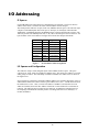
I/O Addressing
IP Spaces
I/O and ID addressing on the VIPC618 is determined by two elements. The first is the base
address of the carrier. Second is the offset of the IP and the desired subspace.
The 1024 bytes the VIPC618 occupies in the A16 VMEbus short I/O space is divided into eight
subspaces. Each IndustryPack has an I/O space of 128 bytes, or 0x80 bytes in hexadecimal.
Additionally, each IndustryPack has an ID PROM space occupying the adjacent 128 bytes. The
VIPC618 provides four IndustryPacks slots, A, B, C & D. The I/O spaces start on offsets of 256
bytes from the carrier base address. The figure below shows the subspace allocations.
Address
I/O Base +
Offset
0x0000
Assignment
IP A I/O Space
Default
0x6000
I/O Base +
0x0080
IP A ID Space
0x6080
I/O Base +
0x0100
IP B I/O Space
0x6100
I/O Base +
0x0180
IP B ID Space
0x6180
I/O Base +
0x0200
IP C I/O Space
0x6200
I/O Base +
0x0280
IP C ID Space
0x6280
I/O Base +
0x0300
IP D I/O Space
0x6300
I/O Base +
0x0380
IP D ID Space
0x6380
Figure 3.
IP I/O Address Offset Assignments
I/O Spaces and Configuration
The VIPC618 occupies 1024 contiguous bytes in the VMEbus short I/O space. This space
consists of 64, 16-bit, words for each IP's I/O and ID space. The carrier base address is set with
shunt groups E3 and E7. The relationship of shunts to VMEbus A16 address lines is shown in
the figure below.
Select signals are generated by comparing VMEbus address lines with the shunt group values. A
shunt installed between E3 and E7 selects a given address line as zero. A shunt removed selects
the address line as a one. Thus, a carrier base address of 0x0000 is selected when all seven
shunts are installed, and carrier base address of 0xFC00 is selected when all seven shunts are
removed. The VIPC618 may be located on any 1024 byte, or 0x400 hex, boundary however;
GreenSpring recommends the common practice of locating VME carriers on 4096 byte, or
0x1000, boundaries.
10
Shunt Loc.
E3.1 to E7.1
Add. Line
A09
Default
IN
Value
0
E3.2 to E7.2
A10
IN
0
E3.3 to E7.3
E3.4 to E7.4
E3.5 to E7.5
A11
A12
A13
IN
IN
OUT
0
0
1
E3.6 to E7.6
E3.7 to E7.7
A14
A15
OUT
IN
1
0
Figure 4.
I/O Base Address Shunt Settings
Default I/O Base Address = 0x6000
VIPC618s are shipped with the default I/O base address set to 0x6000. Please examine the
VIPC618 assembly diagram which shows shunt group locations and default settings. All shunt
groups and through hole components have square solder pads on pin number one to improve
visual orientation. For new system development and debug, we recommend starting with the
0x6000 default address to test carriers and IPs before re-configuration to other locations.
11
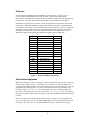
ID Spaces
All IPs must have an ID PROM. This ID PROM is at least 32 bytes. It may be larger. It
provides certain fixed information about the IP, which is defined in the IndustryPack
Specification. This information includes the IP's manufacturer, model code, and manufacturing
revision level. It may also include driver identification codes and calibration information.
ID PROMs are typically used by software for auto configuration, auto calibration, and revision
maintenance. Additional configuration management functions are possible. The ID PROM is
not required to be accessed, nor its information used by the host software. However, since the IP
PROM may contain critical calibration or configuration information, software usage is highly
encouraged. The figure below shows the required information in each ID PROM. See the
IndustryPack Specification and the User Manual for each IP for more information.
Address
0x3F
Description
0x2*nn+1
0x2*nn-1
User Space
0x19
0x17
0x15
0x13
0x11
0x0F
0x0D
0x0B
0x09
0x07
IP Module Specific Space
CRC
Number of bytes used
Driver ID, high byte
Driver ID, low byte
Reserved
Revision
Model Number
Manufacturer ID
ASCII ”C” for 8 MHz
or ASCII "H" for 32 MHz
ASCII ”A”
ASCII ”P”
ASCII ”I”
0x05
0x03
0x01
Contents
= nn
0x00
0x43
or 0x48
0x41
0x50
0x49
Figure 5. Required ID PROM Information
Other Addressing Issues
Many IPs use only the low order, or odd, byte. For these IndustryPacks the bytes are accessed at
location offsets of 0x01, 0x03, etc. This odd byte I/O convention is a Motorola 68000 family
convention and VMEbus standard. Furthermore, Motorola processors and VMEbus use so called
"Big Endian" byte ordering, that is; in a 16 bit word, the bits are ranked in descending order
from left to right (i.e. A15..A8 A 7 ..A0). On "Little Endian" processors, like Intel products, the
byte order is reversed; the low order byte is on the left (i.e. A7 ..A0 A 15..A8), or on even addresses.
In systems using Little Endian CPUs this difference can cause considerable confusion and should
be noted.
IPs are not required to decode all of their allotted I/O space. In this case accessing undecoded
space, or empty IP slots, will cause a VMEbus BERR generated by the offending CPU's bus time
out circuitry. If a CPUs time out is disabled, BERR will not occur, and the bus will "hang."
12
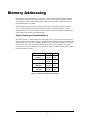
Memory Addressing
IndustryPacks may contain memory as well as I/O. VIPC618 supports both VMEbus standard
memory space (A24:D16) and extended memory space (A32:D16). In the A24 space VIPC618
can be configured from 128k to eight megabytes per IP. In the A32 space VIPC618 provides a
fixed eight megabytes per IP slot.
Memory addressing on the VIPC618 consists of three parts: First enable, or disable, memory
space. Second, set the carrier and IP memory sizes. And last, set the base address. For A32
applications the size step is not required. Please examine the VIPC618 assembly diagram which
shows shunt group locations and default settings.
Step 1: Enabling or Disabling Memory
The memory access is enabled with the E1 shunt group. The two locations are labeled A24 and
A32 on the silk screen for quick reference. Installing a shunt in the E1.A24 location enables A24
standard memory space access. Installing a shunt in the E1.A32 location enables A32 extended
memory space access, this is the factory default setting. VIPC618 only supports one type of
memory space per carrier. Install only one shunt the E1 group. To disable memory access remove
the shunt from the E1 group.
Memory Access
None
(disabled)
Standard A24:16
Extended A32:D16
DEFAULT
Not
Allowed
Location
E1.A32
E1.A24
E1.A32
E1.A24
E1.A32
E1.A24
E1.A32
E1.A24
Shunt
OUT
OUT
OUT
IN
IN
OUT
IN
IN
Figure 6. Memory Enable Shunts Settings
13
Step 2: Setting Carrier and IP Memory Sizes
Size settings are required for A24 addressing only. A32 users may disregard this section and skip
to Step 3. For A24 applications shunt group E2 selects individual IP memory size. This can range
from 128k to two megabytes per IP. The size of the largest IP on the carrier must be chosen. E2
shunt settings are not assigned in any particular order therefore the chart below must be used.
IP Memory Size
128 kilobytes
DEFAULT
256 kilobytes
512 kilobytes
1 megabyte
2 megabytes
Figure 7.
Location
Shunt
E2.1 to E2.2 OUT
E2.3 to E2.4
IN
E2.5 to E2.6
IN
E2.1 to E2.2
E2.3 to E2.4
E2.5 to E2.6
E2.1 to E2.2
E2.3 to E2.4
E2.5 to E2.6
E2.1 to E2.2
E2.3 to E2.4
E2.5 to E2.6
E2.1 to E2.2
E2.3 to E2.4
E2.5 to E2.6
IN
OUT
IN
OUT
OUT
IN
IN
IN
OUT
OUT
IN
OUT
IP Memory Size Shunt Settings
14
Shunts E4, E5 & E8 select the carrier memory size. On VIPC618, this is always four times the IP
memory size. IP memory size should be determined first. Briefly, these three shunt groups route
comparator inputs to VME address lines or short input pairs to identical states. To determine
shunt settings; use the chart below.
Total VIPC618
Memory Size
512 kilobytes
DEFAULT
1 megabyte
2 megabytes
IP Size
IP Slot
128 k
128 k
128 k
128 k
A
B
C
D
IP Location
Base +
0x000000
0x020000
0x040000
0x060000
Install
Shunts
E8.1 to
E8.2 to
E5.1
E5.2
E5.3
E5.4
E5.5
E5.6
E5.1
E5.2
E5.3
E5.4
E5.5
E5.6
E5.1
E5.2
E5.3
E5.4
E5.5
E5.6
E5.1
E5.2
E5.3
E5.4
E5.5
E5.6
E5.1
E5.2
E5.3
E5.4
E5.5
E5.6
256 k
256 k
256 k
256 k
A
B
C
D
0x000000
0x040000
0x080000
0x0C0000
E8.1 to
E8.2 to
E8.3 to
512 k
512 k
512 k
512 k
A
B
C
D
0x000000
0x080000
0x100000
0x180000
E8.1 to
E8.2 to
E8.3 to
E8.4 to
4 megabytes
1 Meg
1 Meg
1 Meg
1 Meg
A
B
C
D
0x000000
0x100000
0x200000
0x300000
E8.1 to
E8.2 to
E8.3 to
E8.4 to
E8.5 to
8 megabytes
2 Meg
2 Meg
2 Meg
2 Meg
A
B
C
D
0x000000
0x200000
0x400000
0x600000
E8.1 to
E8.2 to
E8.3 to
E8.4 to
E8.5 to
E8.6 to
Figure 8.
Carrier Memory Size Shunt Settings
15
from
to E4.3
to E4.4
to E4.5
to E4.6
to E4.4
to E4.5
to E4.6
to E4.5
to E4.6
to E4.6
Step 3: Setting Memory Base Address
The base address for the A32 or A24 spaces are both set with the same shunt groups: E20 and
E21. High speed address decoders use the value of these settings to select the carrier and IP slot.
A shunt installed between the E20 and E21 groups selects a given address line as zero. A shunt
removed selects the address line as a one. Thus for A24 memory, a base address of 0x000000 is
created when all seven shunts are installed. A base address of 0xFE0000 is created when all
seven shunts are removed. Similarly for A32 memory, a base address of 0x00000000 is created
when all seven shunts are installed. A base address of 0xFE000000 is created when all seven
shunts are removed. The factory default memory base address is 0xD00000 in the A24 space,
and 0xD0000000 in the A32 space. The correspondence between shunt locations and VME
address lines is shown in the figure below.
Shunt
Location
E20.1 to E21.1
A24 Space
Address Line
NC
A32 Space
Address Line
NC
Default
Setting
Binary
Value
E20.2 to E21.2
E20.3 to E21.3
E20.4 to E21.4
E20.5 to E21.5
E20.6 to E20.6
E20.7 to E21.7
E20.8 to E21.8
A17
A18
A19
A20
A21
A22
A23
A25
A26
A27
A28
A29
A30
A31
IN
IN
IN
OUT
IN
OUT
OUT
0
0
0
1
0
1
1
Figure 9. Memory Base Address Shunt Settings
Base Address Defaults: A24 = 0xD00000, A32 = 0xD0000000
During VIPC618 memory cycles the higher order VMEbus address lines are routed directly to the
IP address lines. This simplifies matters by eliminating complicated address re-mapping and
decoding wait states. Additionally, the memory sizing scheme on the VIPC618 uses the memory
base address shunt values. When using memory, these two factors require the memory base
address of the carrier be on a boundary equal to the sum of all memory space available on
the carrier. For A32 applications the VIPC618 must be on a 32 megabyte boundary (i.e.
0x00000000, 0x02000000, 0x04000000...etc.) For A24 applications the aggregate memory
capacity of the VIPC618 must be calculated.
For an A24 space example consider the following: A VIPC618 with two memory IPs, the largest
of which being one megabyte, would require configuring the carrier for one megabyte per slot.
The sum of memory capacity on the carrier would then be four megabytes, or one megabyte per
slot. The memory base address (and IP slot A base) must be on a four megabyte boundary in the
A24 space (i.e. 0x000000, 0x400000, 0x800000...etc.). The slot B base would be at carrier base
+ one megabyte (i.e. 0x100000, 0x500000, 0x900000...etc.).
16
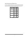
A24 Memory Configuration Example
Consider the following example where two memory IPs are installed in an A24 application: A
256k IP-JEDEC and a 1 megabyte IP-NVRAM are to be installed on a VIPC618, in IP slots A
and B respectively. First install a shunt in the E1.A24 location to enable A24 access. The biggest
IP is IP-NVRAM at 1 megabyte. Use the IP Memory size able to configure E2 for 1 megabyte
per IP. Next the sum of memory capacity of the carrier is four times the biggest IP memory size,
or four megabytes in this case. Use shunt groups E4, E5 & E8 settings shown in the Carrier
Memory Size table to configure the carrier memory size for four megabytes. Finally determine a
memory base address. Because the carrier memory size is four megabytes, the memory base
address must be located on a four megabyte boundary (i.e. 0x0000000, 0x0400000,
0x0800000...etc.). Use shunt groups E20 and E21 to configure the memory base address. If we
arbitrarily choose a base of 0x0400000: The IP-JEDEC, in slot A, would then occupy the A24
space from 0x0400000 to 0x043FFFF. The IP-NVRAM , in slot B, would occupy the A24 space
from 0x0500000 to 0x05FFFFF. The resulting shunt configurations are shown in the table below.
Memory Access
E1.A32
E1.A24
E2.1
E2.3
E2.5
OUT
IN
IP Memory Size
to E2.2
OUT
to E2.4
IN
to E2.6
OUT
Carrier Memory Size
E8.1 to
E5.1
E8.2 to
E5.2
E8.3 to
E5.3
E8.4 to
E5.4
E8.5 to
E5.5
E5.6
to E4.6
Memory Base Address
E20.1 to
E21.1
OUT
E20.2 to
E21.2
IN
E20.3 to
E21.3
IN
E20.4 to
E20.5 to
E21.4
E21.5
IN
IN
E20.6 to
E20.7 to
E20.8 to
E21.6
E21.7
E21.8
IN
OUT
IN
Figure 10. A24 Memory Configuration Example
17
Interrupts
IndustryPacks are able to generate up to two interrupt requests each. Each interrupt request is
serviced by an interrupt acknowledge cycle from the host CPU. During this cycle the requesting
IP responds with an interrupt vector. The host CPU uses this vector to begin executing an
interrupt service routine. This routine must access the requesting IP in such a way as to remove
the interrupt request.
There are seven levels of interrupt requests on the VMEbus. IRQ7 is the highest, and is normally
reserved for non-maskable requests. IRQ1 is the lowest level.
Configuration blocks are provided on the VIPC618 to route the eight possible interrupt requests
from the IndustryPacks to the seven VMEbus levels. Similarly, matching configuration blocks
are provided to route the seven interrupt acknowledge cycles to the requesting IP.
The simplest wiring scheme is to use a shunt to connect each pin of E10 straight across to the
corresponding pin of E9. This is the factory default configuration. The correspondence of IP
interrupt requests to VMEbus IRQ levels is then determined by reading across each line of the
table below. Many alternative mappings are possible by using wire-wrap™ wires instead of
shunts. Each encoding map provided by the E10-E9 configuration block must match a
corresponding decoding map provided by the E11-E12 configuration block discussed below.
IP
Slot
A
A
B
B
C
C
D
IP IRQ
Level
0
1
0
1
0
1
0
E10
Pin
1
2
3
4
5
6
7
D
1
8
Figure 11.
E9
Pin
1
2
3
4
5
6
7
VMEbus
IRQ Level
IRQ1
IRQ2
IRQ3
IRQ4
IRQ5
IRQ6
IRQ7
NONE
Interrupt Encoding Configuration Block
Note that the configuration block E10-E9 provides only for one-to-one mappings between IP
requests and VMEbus IRQ levels. More complex mappings are possible by using a user-provide
interrupt encoding PLD or equivalent device in socket U11. Contact the factory Application
Engineering department for more information. When using an U11 mapping PLD, be sure that
(1) the jumpers in E10-E9 are removed, and (2) that PLD U17 provides a complementary
decoding map.
18
The figure below shows the wiring of the interrupt decoding configuration block. This figure
also shows the factory default programming of the interrupt decoding PLD U17. The simplest
wiring scheme is to use a shunt to connect each pin of E11 straight across to the corresponding
pin of E12. This is the factory default configuration. The correspondence of VMEbus interrupt
acknowledge levels to IndustryPack Interrupt Selects is then determined by reading across each
line of the table in the figure. Many alternative mappings are possible by using wire-wrap™
wires instead of shunts. Each decoding map provided by the E11-E12 configuration block
must match the corresponding encoding map provided by the E10-E9 configuration block
discussed above.
VMEbus
IACK cycle
IRQ7
IRQ6
E11
pin
1
2
E12
pin
1
2
IP
Slot
D
C
IntSel*
Level
0
1
IRQ5
IRQ4
IRQ3
3
4
5
3
4
5
C
B
B
0
1
0
IRQ2
IRQ1
6
7
6
7
8
A
A
D
1
0
1
Figure 12.
Interrupt Decoding Configuration Block
Interrupt selection within an IndustryPack as accomplished with the A1 address line to each IP.
A1 low corresponds to Interrupt Select 0; A1 high corresponds to Interrupt Select 1. During I/O
and Memory cycles A1 to the IPs must match A1 from the VMEbus, of course. PLD U17
generates A1 to the four IP to implement these functions.
19
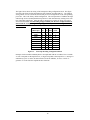
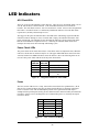
LED Indicators
ACK Flash LEDs
There are six green LED indicators on the VIPC618. There are four "ACK flash" LEDs, one for
each IP, and two Power Check indicators. ACK flash LEDs flash after successful IP bus
transfers. The ACK flash "one shot" lasts for one third of a second. Accesses more frequent than
three times a second will show as a continuously illuminated indicator. The ACK flash LEDs
respond to I/O, memory and interrupt accesses.
The trigger for the pulse stretcher that drives the LEDs is the acknowledge signal from the IPs.
If the host software attempts to access a location that is empty, the indicator LED on the front
panel will not light. The indicators do not show that the VIPC618 is being selected, but rather
that the associated IP has completed an access. Similarly, the indicator LEDs do not show
interrupts asserted, but do show interrupt acknowledge cycles.
Power Check LEDs
The power check circuit detects blown fuses or line faults on the two adjacent IP slots. When the
LED is lit, the IP slots are OK and ready for use. The upper PWR LED shows status for IP slots
A and B, and the lower PWR LED shows status for IP Slots C & D. The following table can be
used to isolate power faults with the aid of the power check LEDs:
Upper
PWR LED
on
Lower
PWR LED
on
on
off
off
off
on
off
Figure 13.
Condition
OK, Ready to Use
C & D 5V, Check F3 & F4
A & B 5V, Check F1 & F2
+12V or –12V, Check F5 &
F6
Diagnostics with Power Check LEDs
Fuses
The fuses used on VIPC618 are 1 Amp, 1206 surface mount (Little fuse p/n R429.001). All IP
Slots are fuse protected. Blown fuses may be detected with a DVM. Use the chart in the figure
below to associate a fuse with an IndustryPack position. Fuse replacement should only be
attempted with equivalent parts and by persons skilled in surface-mount assembly and Anti-ESD
procedures. Factory service and diagnostics are recommended, please see warranty and repairs
section for details.
Fuse
F1
Power Bus
+5V IP A
Value
1.0 Amp
F2
F3
F4
+5V IP B
+5V IP C
+5V IP D
1.0 Amp
1.0 Amp
1.0 Amp
F5
–12V IP A,B,C,D 1.0 Amp
F6
+12V IP A,B,C,D 1.0 Amp
Figure 14.
Fuse Locations and Ratings
20
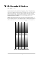
P2 I/O, Grounds & Strobes
I/O on P2 Connector
Normally all four IPs have their I/O cabling via the front panel. However, IndustryPack slots C
and D may also have their I/O connected via the VMEbus P2 connector. This I/O may be used
whether or not a VMEbus P2 backplane is installed. The VMEbus leaves rows A and C of the P2
connector open for this I/O use. Note however that some systems, such as VSB, use these 64
lines for a secondary bus. The XM-CE-P2 transition module provides a reliable and convenient
mechanism for accessing these signals. Please contact GreenSpring computers or your
international distributor for information.
Caution: IndustryPack slot D is hard wired to rows A and C of the VMEbus P2 connector. If
the user's system has rows A and C of P2 committed to another use then either slot D must be left
empty, or a non-I/O IP must be used in slot D. Most memory IPs from GreenSpring Computers
do not use any I/O lines. The IP slot D I/O to VMEbus P2 mapping is shown in the figure below.
Slot D
IP I/O
1
3
5
7
9
11
VMEbus
P2
C1
C2
C3
C4
C5
C6
Slot D
IP I/O
2
4
6
8
10
12
VMEbus
P2
A1
A2
A3
A4
A5
A6
13
15
17
C7
C8
C9
14
16
18
A7
A8
A9
19
21
23
25
27
29
31
C10
C11
C12
C13
C14
C15
C16
20
22
24
26
28
30
32
A10
A11
A12
A13
A14
A15
A16
33
35
C17
C18
34
36
A17
A18
37
39
41
C19
C20
C21
38
40
42
A19
A20
A21
43
45
C22
C23
44
46
A22
A23
47
49
C24
C25
48
50
A24
A25
Figure 15.
IP Slot D to VMEbus P2 Connections
21
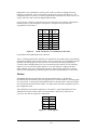
IndustryPack C may optionally be connect to pins on the P2 connector, although the factory
default is no connection. Up to 14 signals from the IP in slot C may be assigned to P2. The
configuration block E13-E14-E15 is used to implement this interconnection. In most cases wirewrap™ will be the most convenient implementation method.
E13 has 50 pins, which are connected to the 50 pins of the Slot C I/O connector and numbered
identically (pin 1 to pin 1 through pin 50 to pin 50). The figure below shows the Pin
Assignments for E14 and E15.
E14 VMEbus E15 VMEbus
Pin
P2
Pin
P2
1
C26
1
A26
2
C27
2
A27
3
C28
3
A28
Figure 16.
4
C29
4
A29
5
6
7
C30
C31
C32
5
6
7
A30
A31
A32
E14 & E15 (IP Slot C) to VMEbus P2 Connections
Ground Planes under IndustryPack I/O Connectors
There is a floating ground plane under the I/O connectors for IPs A and B, and a second floating
ground plane under the I/O connectors for IPs C and D. These planes are for shielding and noise
reduction. The floating planes on the carrier can be connected to the main ground plane at
several locations. Installing shunts E16 or E18 connects the plane under IP A & B. Installing
shunts E17 or E19 connects the plane under IP C & D The VIPC618 is shipped with these
shunts installed. Users can re-configure these shunts as desired. Note all I/O lines are routed
directly to the IndustryPacks, ground I/O signals are provided by IndustryPacks, not the carrier.
Strobes
Each IndustryPack has one pin on the logic interface labeled "Strobe." The Interface
Specification does not define this pin, but suggests that it be used for alternative clocking signals
in or out of an IP. A four position configuration block E6 is provided on the VIPC618 to permit
user interconnection of the IP Strobe signals. The figure below shows the assignment of pins on
this configuration block.
This information is provided for completeness. The "Strobe*" signal nomenclature has been
abandoned in current revisions of the VITA-4 Specification. They may be referred to as
"reserved". The "Strobe*" signals are seldom used.
E6 Pin
E6.1
E6.2
Strobe*
IP Slot A
IP Slot B
E6.3
E6.4
IP Slot C
IP Slot D
Figure 17.
Strobe Signals
22
IP Logic Interface
The VITA-4 specification is the definitive reference for the IP bus logic interface. When this
manual was written, the current revision was:
ANSI/VITA 4-1995
Specification Revision 1.0
IP Mezzanine Module Standard
This document, or its successor, is available from GreenSpring or VITA. VITA can be contacted
at the following address.
VITA Standards Organization
10229 North Scottsdale Road, Suite B
Scottsdale Az. 85252
Voice: 602-951-8866
Fax: 602-951-0720
For quick reference, the table below shows the IP Logic pin assignments. Some of these signals
may not be supported on this product.
Pin #
1
3
5
7
9
11
13
15
17
19
21
23
25
Signal
GND
Reset*
D1
D3
D5
D7
D9
D11
D13
D15
BS1*
+12V
GND
Pin #
2
4
6
8
10
12
14
16
18
20
22
24
Figure 18.
Signal
CLK
D0
D2
D4
D6
D8
D10
D12
D14
BS0*
- 12V
+ 5V
Pin #
Signal
Pin #
26
GND
27
28
R/W*
29
30
DMAReq0*
31
32
DMAReq1*
33
34
DMAck*
35
36
Reserved
37
38
DMAEnd*
39
40
Error*
41
42
IntReq0*
43
44
IntReq1*
45
46
Strobe*
47
48
Ack*
49
50
GND
IP Logic Interface Pin Assignment
23
Signal
+ 5V
IDSel*
MemSel*
IntSel*
IOSel*
A1
A2
A3
A4
A5
A6
Reserved
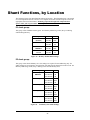
Shunt Functions, by Location
The following figures list shunt functions indexed by location. The information here is presented
for visual inspection and cross reference. For complete discussions of functions please review the
appropriate sections of this manual. All shunt groups and through hole components have
square solder pads on pin number one to improve visual orientation.
E1 shunt group:
This group selects VMEbus memory space. See Memory Addressing section, Step 1: Enabling
and Disabling Memory.
Memory Access
None
(disabled)
Standard A24:16
Extended A32:D16
DEFAULT
Not
Allowed
Location
E1.A32
E1.A24
E1.A32
E1.A24
E1.A32
E1.A24
E1.A32
E1.A24
Shunt
OUT
OUT
OUT
IN
IN
OUT
IN
IN
Figure 19. Memory Enable Shunt Settings
E2 shunt group:
This group selects the IP Memory size. Size settings are required for A24 addressing only. E2
shunt settings are not assigned in any particular order therefore the chart below must be used. See
Memory Addressing section, Step 2: Setting Carrier and IP Memory Sizes.
IP Memory Size
128 kilobytes
DEFAULT
256 kilobytes
Location
Shunt
E2.1 to E2.2 OUT
E2.3 to E2.4
IN
E2.5 to E2.6
IN
E2.1 to E2.2
IN
E2.3 to E2.4 OUT
E2.5 to E2.6
IN
512 kilobytes
E2.1 to E2.2
E2.3 to E2.4
E2.5 to E2.6
OUT
OUT
IN
1 megabyte
E2.1 to E2.2
E2.3 to E2.4
E2.5 to E2.6
IN
IN
OUT
2 megabytes
E2.1 to E2.2
E2.3 to E2.4
E2.5 to E2.6
OUT
IN
OUT
Figure 20.
IP Memory Size Shunt Settings
24
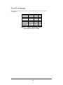
E3 and E7 shunt groups:
These shunts select the I/O base address. See I/O Addressing section; I/O Spaces and
Configuration
Shunt Loc.
E3.1 to E7.1
Add. Line
A09
Default
IN
Value
0
E3.2 to E7.2
A10
IN
0
E3.3 to E7.3
E3.4 to E7.4
E3.5 to E7.5
A11
A12
A13
IN
IN
OUT
0
0
1
E3.6 to E7.6
E3.7 to E7.7
A14
A15
OUT
IN
1
0
Figure 21.
I/O Base Address Shunt Settings
Default I/O Base Address = 0x6000
25
E4, E5 and E8 shunt groups:
These shunts select the total carrier memory size. Briefly, these three shunt groups route
comparator inputs to VME address lines or short input pairs to identical states. See Memory
Addressing section, Step 2: Setting Carrier and IP Memory Sizes.
Total VIPC618
Memory Size
512 kilobytes
DEFAULT
1 megabyte
2 megabytes
IP Size
IP Slot
128 k
128 k
128 k
128 k
A
B
C
D
IP Location
Base +
0x000000
0x020000
0x040000
0x060000
Install
Shunts
from
E8.1 to
E8.2 to
E5.1
E5.2
E5.3
E5.4
E5.5
E5.6
to E4.3
to E4.4
to E4.5
to E4.6
256 k
256 k
256 k
256 k
A
B
C
D
0x000000
0x040000
0x080000
0x0C0000
E8.1 to
E8.2 to
E8.3 to
512 k
512 k
512 k
512 k
A
B
C
D
0x000000
0x080000
0x100000
0x180000
E8.1 to
E8.2 to
E8.3 to
E8.4 to
4 megabytes
1 Meg
1 Meg
1 Meg
1 Meg
A
B
C
D
0x000000
0x100000
0x200000
0x300000
E8.1 to
E8.2 to
E8.3 to
E8.4 to
E8.5 to
8 megabytes
2 Meg
2 Meg
2 Meg
2 Meg
A
B
C
D
0x000000
0x200000
0x400000
0x600000
E8.1 to
E8.2 to
E8.3 to
E8.4 to
E8.5 to
E8.6 to
Figure 22.
E5.1
E5.2
E5.3
E5.4
E5.5
E5.6
E5.1
E5.2
E5.3
E5.4
E5.5
E5.6
E5.1
E5.2
E5.3
E5.4
E5.5
E5.6
E5.1
E5.2
E5.3
E5.4
E5.5
E5.6
Carrier Memory Size Shunt Settings
26
to E4.4
to E4.5
to E4.6
to E4.5
to E4.6
to E4.6
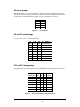
E6 header group:
This group provides user access to the Strobe* signal defined in the IndustryPack specification.
The function of these signals will be defined by the IP. The header is intended for connections to
external signals, no shunt settings are defined See I/O, Grounds & Strobes section
E6 Pin
E6.1
Strobe*
IP Slot A
E6.2
IP Slot B
E6.3
E6.4
IP Slot C
IP Slot D
Figure 23.
Strobe Signals
E9 and E10 shunt groups
These shunts select outgoing VMEbus IRQ levels. The factory configuration is straight across
(i.e. E9.1 to E10.1 etc...) See Interrupts section.
IP
Slot
A
A
B
B
C
C
IP IRQ
Level
0
1
0
1
0
1
E10
Pin
1
2
3
4
5
6
E9
Pin
1
2
3
4
5
6
VMEbus
IRQ Level
IRQ1
IRQ2
IRQ3
IRQ4
IRQ5
IRQ6
D
D
0
1
7
8
7
IRQ7
NONE
Figure 24.
Interrupt Encoding Configuration Block
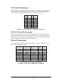
E11 and E12 shunt groups
During the IACK cycle these shunts select the returning IntSel* signal destination. The factory
configuration is straight across (i.e. E11.1 to E12.1 etc...) See Interrupts section.
VMEbus
IACK cycle
IRQ7
E11
pin
1
E12
pin
1
IP
Slot
D
IntSel*
Level
0
IRQ6
IRQ5
2
3
2
3
C
C
1
0
IRQ4
IRQ3
4
5
4
5
B
B
1
0
IRQ2
IRQ1
6
7
6
7
A
A
1
0
8
D
1
Figure 25.
Interrupt Decoding Configuration Block
27
E13, 14 and E15 shunt groups
These groups are for user defined connection of the IP slot C I/O connector and the VMEbus P2
connector. VIPC618 is shipped with these locations vacant. See P2 I/O, Grounds & Strobes
section. E13 pins are connected directly the IP slot C I/O lines, "pin 1 to pin 1, etc...".
E14 VMEbus E15 VMEbus
Pin
P2
Pin
P2
1
C26
1
A26
Figure 26.
2
C27
2
A27
3
4
C28
C29
3
4
A28
A29
5
C30
5
A30
6
7
C31
C32
6
7
A31
A32
E14 & E15 (IP Slot C) to VMEbus P2 Connections
E16, E17, E18 and E19 shunt groups
These shunts connect the floating ground planes underneath the I/O connectors to the main
ground plane in the VIPC618. See P2 I/O, Grounds & Strobes section. Installing shunts E16 or
E18 connects the plane under IP A & B. Installing shunts E17 or E19 connects the plane under
IP C & D. The VIPC618 is shipped with these shunts installed.
E20 and E21 shunt groups
These shunts select the A24 and A32 memory base address. See Memory Addressing section,
Step 3: Setting Memory Base Address.
Shunt
Location
E20.1 to E21.1
E20.2 to E21.2
E20.3 to E21.3
E20.4 to E21.4
A24 Space
Address Line
NC
A17
A18
A19
A32 Space
Address Line
NC
A25
A26
A27
Default
Setting
Binary
Value
IN
IN
IN
0
0
0
E20.5 to E21.5
E20.6 to E20.6
E20.7 to E21.7
A20
A21
A22
A28
A29
A30
OUT
IN
OUT
1
0
1
E20.8 to E21.8
A23
A31
OUT
1
Figure 27. Memory Base Address Shunt Settings
Base Address Defaults: A24 = 0xD00000, A32 = 0xD0000000
28
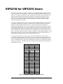
VIPC618 for VIPC610 Users
The VIPC618 is the direct evolutionary successor to GreenSpring Computer's popular VIPC610
carrier. The VIPC618 was designed to be 100% backward compatible with the VIPC610. The
VIPC610 is no longer recommended for new designs and will be phased out of production. The
VIPC618 maintains all the functionality of the VIPC610 and adds improved features. Four
commonly requested improvements were implemented on the VIPC618; VMEbus extended
memory access (A32:D16), Independent I/O and Memory base address selection, latching
connectors and power check LEDs.
The VIPC618 implementation of Short I/O (A16:D16) and Standard Memory (A24:D16) spaces
is functionally identical to the VIPC610. VMEbus interface, addressing, memory sizing and
interrupts are implemented with the same logic. Two shunt groups have been added to
implement Extended Memory access. First, A completely new address decoder has been added
for the high order address lines. The I/O base address and A24 memory base address can now be
selected independently. Both A32 and A24 memory base addresses are selected with E20 and
E21 shunt groups. Secondly, the E1 shunt has been expanded into two separate shunts; E1.A24
and E1.A32. On the old VIPC610 the E1 shunt was installed to enable Standard Memory. On the
VIPC618 the E1 shunt has one position for A24 Standard Memory and one position for A32
Extended Memory. Removing the E1 shunt disables memory access.
To configure the VIPC618 as a drop in replacement for the VIPC610 the I/O base address
selection must match the Memory base address. This is accomplished by configuring the E20 &
E21 shunt groups and the E3 & E7 groups to identical values. The E1.A24 shunt must also, of
course, be installed to enable A24 access. Additionally the VIPC618 is set with a factory default
memory base address of 0xD00000. This must be changed to 0x600000 if the default VIPC610
configuration is desired.
E1.A32
E1.A24
Memory Enable
OUT
IN
I/O Base Address
E3.1 to
E7.1
IN
E3.2 to
E7.2
IN
E3.3 to
E3.4 to
E7.3
E7.4
IN
IN
E3.5 to
E3.6 to
E3.7 to
E7.5
E7.6
E7.7
OUT
OUT
IN
Memory Base Address
E20.1 to
E21.1
NC
E20.2 to
E20.3 to
E21.2
E21.3
IN
IN
E20.4 to
E20.5 to
E20.6 to
E21.4
E21.5
E21.6
IN
IN
OUT
E20.7 to
E20.8 to
E21.7
E21.8
OUT
IN
Figure 28. VIPC618 Configured for VIPC610 Defaults
29
Construction and Reliability
IndustryPacks were conceived and engineered for rugged industrial environments. The VIPC618
is constructed out of 0.062 inch thick FR4 material. The six copper layers consist of a ground
plane, a power plane and four digital signal planes.
Through hole component mounting is used. IC sockets use gold plated screw–machine pins. High
insertion and removal forces are required, which assists in keeping components in place. If the
application requires unusually high reliability or is in an environment subject to high vibration,
the user may solder the four corner pins of each socketed IC into the socket, using a grounded
soldering iron. Shunts may be replaced with wire–wrap® wires if desired.
The IndustryPack connectors are keyed, shrouded and gold plated on both contacts and
receptacles. They are rated at 1 Amp per pin, 200 insertion cycles minimum. These connectors
make consistent, correct insertion easy and reliable.
The IP is secured to the carrier with four metric M2 stainless steel screws. The heads of these
screws are countersunk into the IP. The four screws provide significant protection against shock,
vibration, and incomplete insertion. For most applications they are not required.
The IndustryPack provides a low temperature coefficient of 0.89 W/°C for uniform heat. This is
based on the temperature coefficient of the base FR4 material of .31 W/m–°C, and taking into
account the thickness and area of the IP. This coefficient means that if 0.89 Watts is applied
uniformly on the component side, that the temperature difference between the component and the
solder side is one degree Celsius.
30
Warranty and Repair
GreenSpring Computer warrants this product to be free from defects in workmanship and
materials under normal use and service and in its original, unmodified condition, for a period of
one year from the time of purchase. If the product is found to be defective within the terms of this
warranty, GreenSpring Computer's sole responsibility shall be to repair, or at GreenSpring
Computer's sole option to replace, the defective product. The product must be returned by the
original customer, insured, and shipped prepaid to GreenSpring Computers. All replaced
products become the sole property of GreenSpring Computers.
GreenSpring Computer's warranty of and liability for defective products is limited to that set
forth herein. GreenSpring Computers disclaims and excludes all other product warranties and
product liability, expressed or implied, including but not limited to any implied warranties of
merchandisability or fitness for a particular purpose or use, liability for negligence in
manufacture or shipment of product, liability for injury to persons or property, or for any
incidental or consequential damages.
GreenSpring’s products are not authorized for use as critical components in life support devices
or systems without the express written approval of the president of GreenSpring Computers, Inc.
Service Policy
Before returning a product for repair, verify as well as possible that the suspected unit is at fault.
Then call the Customer Service Department for a RETURN MATERIAL AUTHORIZATION
(RMA) number. Carefully package the unit, in the original shipping carton if this is available,
and ship prepaid and insured with the RMA number clearly written on the outside of the
package. Include a return address and the telephone number of a technical contact. For out–of–
warranty repairs, a purchase order for repair charges must accompany the return. GreenSpring
Computers will not be responsible for damages due to improper packaging of returned items. For
service on GreenSpring Products not purchased directly from GreenSpring Computers contact
your reseller. Products returned to GreenSpring Computers for repair by other than the original
customer will be treated as out–of–warranty.
Out of Warranty Repairs
Out of warranty repairs will be billed on a material and labor basis. The current minimum repair
charge is $100. Customer approval will be obtained before repairing any item if the repair
charges will exceed one half of the quantity one list price for that unit. Return transportation and
insurance will be billed as part of the repair and is in addition to the minimum charge.
For Service Contact:
Customer Service Department
GreenSpring Computers
181 Constitution Drive
Menlo Park, CA 94025
(415) 327–1200
(415) 327–3808 fax
31
Specifications
VMEbus Conformance
Revision IEEE P1024/D1.2
VMEbus Form Factor
6U (double high)
IndustryPack® Conformance
ANSI/VITA 4— 1995
Number of IndustryPacks
Four single-high, or
Two double-high
IP ID PROM Mapping
A16, 128 bytes/IP
IP I/O Mapping
A16, 128 bytes/IP
IP Memory Mapping
A24 or A32
Memory Size
None, or 128 kbytes to 4 MB in 6
increments for the A24 space or
32 MB fixed in the A32 space.
VMEbus Interrupts
IRQ1 through IRQ7,
shunt selectable, or User PLD
selectable.
Front panel I/O Interconnect
Four AMPLIMITE 0.050 Series RightAngle Receptacle Headers Without
Rails-With Latch Blocks, 50 position
(part number AMP 749831-5), or
equivalent. Mating part: Shielded
AMPLIMITE 0.050 Series Connectors,
50 position.
VMEbus P2 I/O
All 50 I/O lines from the IP at slot D,
and a user 14 of 50 I/O lines from the
IP at slot C, are available at the P2
connector.
LED Indicators
Six green LED's,
One ACK Flash LED for each slot
Two PWR Check LEDs, A/B and C/D.
Power Requirements
+ 5 V @ 610 mA typical
+12 V @ 0 mA
– 12 V @ 0 mA
Additional power is consumed
by IndustryPacks
Environmental
0o C to 70o C operating
5 to 95% relative humidity (non
condensing)
–10 to + 85o C storage
Size
172 mm deep
232 mm high (incl. front panel)
13.6 mm thick
Weight
0.34 Kg
32