1
HCPL-261 I-060 Technical Data
Appendix A
12
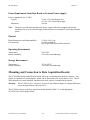
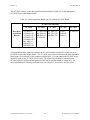
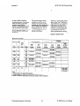
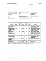
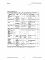
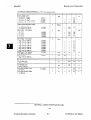
Package Characteristics
Au Typicals at TA = 25?c.
Psnuneter
SP-
Package
Input-output
ho*
Siie d-Pin DIP
Single SO-8
Input-Output
Momentary Withstand Voltage**
VFKl
8-Pin DIP, SO-8
Widebody
OPT 0207
Input-output
&I
&Pin DIP, SO-8
Wldebody
InsulaciOll
RdStZlce
Input-output
Capacitance
%J
8-Pin DIP, SO-8 (
Widebody
1
Input-Input
Insukuion
Leakage Current
IH
Dual Channel
Resbmnce
(Input-Input)
%I
Dual Channel
Capadrance
(Input-InPut)
CH
Dual 8-Pin DIP
DlASO-8
M.~L i Qp. i Max. /
1
I.4
1
2500 /
5000 I
I
5000 !
I
I 10’2 I
10” I 101” /
10’1 1
1 0.6
1 0.5
Vrms
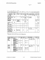
Test Conditions
Fig. / Note
45% RH. t = 5 s,
Vw=3kVdc,T,=25’=C
20,21
RHc5O%,t=lmin,
20,21
20,22
TA= 259:
R
V,, = 500Vdc i
1,m
23
TA = 25°C
TA = 100°C
1
1
Units
PF
f = 1 MHz, TA = 25°C
M-4
RH I 45%, t = 5 s,
v, = 500 v
0.6
0.005
I
24
I
10”
24
R
0.03
, 0.25
PF
f=lMHz
24
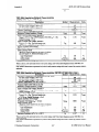
l JEDEC registered data for the 6N13i. The JEDEC Regumation specifies 0°C to 7O’C. HP specifies -4O’C to 85’C.
l Crhe Input-Output Momentary Withstand Voltage is a dielectric voltage ratsng that should not be interpreted as an input-output
continuous voltage rating. For the continuous voltage raring refer to the VDE 0884 Insularion Chamcteristics Table (ii applicable),
your equipment level safety specification or HP Application Note 1074 entitled ‘Optocoupler Input-Output End&e
Voltage.”
tFor 6N137, HCPL26OlR611/2630L2631/4661 only.
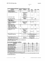
Notes:
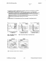
1. EachcharmeI.
2. Peaking circuits may produce Uansient input currents up to 50 mA, 50 ns maximum pulse width,‘provided average current does
not exceed 20 mk
3. Peaking circuits may produce transient input currents up to 50 mA, 50 ns maximum pulse width, provided average current does
not exceed 15 mk
4. Derate linearly above 8OYJfree-air temperature at a rate of 2.7 mWK for the SOIC-8 package.
5. Byparsing of the power supply line is required, with a 0.1 pF ceramic disc capacitor adjacent to each optocoupler as iIlustrated in
Figure 17. Total lead length between both ends of the capacitor and the isolator pins should not exceed 20 mm.
6. The JEDEC registrAon for the 6N137 specifies a rnakwm IOHof 250 nA HP guarantees a maximum Ion of 100 ir.A.
7. The JEDEC registrauon for the 6N137 specifies a ~~~CHOf15~~~~a~~ICCHOf10~
8. The JEDEC registration for the 6N137 specifies a ~~Icc~ofl8mAHPguaranteesa~~Icc~of13mk
9. The J’EDEC registration for the 6Nl37 speci8es a maximum IEL of -2.0 rrA HP guarantees a maximum IEL of -1.6 in4
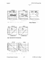
10. The tpm propagation delay is measured from the 3.75 mA point on the fding edge of the input pulse to the 1.5 V point on the
rising edge of the output pulse.
11. The tptq, propagation delay is m-ed
from the 3.75 mA point on the rising edge of the input pulse to the 1.5 V point on the
faIlbug edge of the ollrput pulse.
12. tpg( is equal to the womt case difference in tpm and/or tpLB that will be seen between units at any given tempeiarure and
specified test conditions.
13. See application section titled “Propagation Delay, P&e-Width Distortion and Propagation Delay Skew” for more mformtion.
14. The tm enable propagation delay is measured from the 1.5 V point on the falling edge of the enable input pulse to the 1.5 V
point on the rising edge of the output pulse.
15. The tEm enable propagation delay is measured from the I.5 V point on the rising edge of the enable input puIse co the 1.5 V point
on the faIIing edge of the output pulse.
16. CMn is the maximum tolerable rate of rise of the common mode voltage to assure that the output wiU remain in a high logic state
(i.e., Vo > 2.0 V).
17. CMt is the maximum tolerable iate of fall of the common mode voltage to assure that the output wiU remain in a low logic state
(i.e., Vo c 0.8 v).
18. For sinusoidal voltages. (Idvc.~ 1 / dt)= nfcMVcM(p-p).
0 National Instruments Corporation
A-13
SC-206X Series User Manual