1
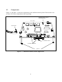
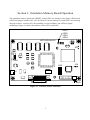
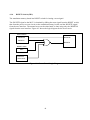
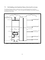
Section 3 Emulation Memory Board Functions
The functions of the emulation memory board are listed in table 3.1.
Table 3.1 Emulation Memory Board Functions
Function
Clock
Specifications
• Iφ (CPU clock) = 133.34 MHz (max.)
• Clock installed in this emulation memory board: 16.6 MHz (EXTAL input)
Substitution
emulation memory
• Capacity: 4 Mbytes (8 blocks of 256 kwords x 16 bits)
• 66.6 MHz (max.) = B (bus clock): Two wait cycles inserted by WCR2
• Can be allocated to the CS0 area
(Substitution memory area: H’00000000 to H’003FFFFF)
• Data bus width can be selected from 16 or 32 bits
(8-bit width is not supported)
User interface
Supported package: 176-pin QFP
Crystal oscillator
Supported frequency for crystal oscillation: 10 MHz to 16.7 MHz
Switch settings
• SW3: Selects the power source
• JP1 and JP3: Select the clock source
• JP4: Selects the CS0 signal output destination
DIP switch settings
• SW2-1 to SW2-3: Selects the clock operating mode
• SW2-4 and SW2-5: Select the bus width for area 0
• SW2-6: Selects the endian
• SW2-7: Selects the ASE mode
• SW2-8: Selects the source of MD0 to MD5
• SW2-9: Selects whether or not to write-protect the substitution emulation
memory
RESET switch
SW1: Issues a RESET signal
LEDs
• LED1: RESET and POWER
• LED2: WAIT and RUN
• LED3: BREQ and NMI
• LED4: STATUS1 and STATUS0
5