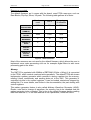
1
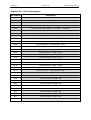
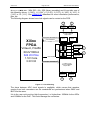
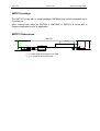
SMT370v2/v3
User Manual
User Manual (QCF42); Version 3.0, 8/11/00; © Sundance Multiprocessor Technology Ltd. 1999
Version 2.0
Page 2 of 46
SMT370v2/v3 User Manual
Revision History
Date
Comments
Engineer
Version
14/02/03
First release
PSR
1.0
08/03/03
Details added about registers and external
signals – figure references – examples.
PSR
1.1
FPGA Firmware changed – ADC/DAC Triggers
and ADC decimators added – SHBA and B 16
or 32 bits.
PSR
1.2
31/03/03
15/05/03
ComPorts description improved – Two
separate options to the board – FPGA Global
reset register added – More comments on
register settings – FPGA utilisation added –
Example code removed
PSR
1.3
01/08/03
Corrects spelling mistakes - adds temperature
measurements – mentions SMT6600 package
PSR
1.4
05/09/03
One link (fig11 was missing)
PSR
1.5
15/10/03
Updated for SMT370v3
PSR
1.6
17/12/03
Pattern generator description a bit confused.
Modified it. Module.
PSR
1.7
18/12/03
Module Height added
PSR
1.8
27/05/04
AWG term added.
PSR
1.9
13/07/04
Input and output stages ADC/DAC schematics
added. ADC input voltage corrected.
PSR
2.0
02/06/05
Figure 13 corrected
PSR
2.1
Version 2.0
Page 3 of 46
SMT370v2/v3 User Manual
Table of Contents
Revision History.......................................................................................................... 2
Table of Contents ....................................................................................................... 3
Contacting Sundance. ................................................................................................ 5
Notes. ......................................................................................................................... 5
Precautions................................................................................................................. 5
Outline description...................................................................................................... 6
Block Diagram - Architecture. ..................................................................................... 7
Architecture Description. ............................................................................................ 8
Virtex FPGA. ........................................................................................................... 9
What the FPGA does........................................................................................... 9
Ressource occupied. ......................................................................................... 10
Memory. ................................................................................................................ 10
ADCs and DAC. .................................................................................................... 11
Clock management. .............................................................................................. 11
Sundance High-speed Bus - SHB......................................................................... 11
SHBA – ADCs. .................................................................................................. 11
SHBB – DAC. .................................................................................................... 12
Communication Ports (ComPorts). ....................................................................... 12
External triggering. ................................................................................................ 12
LEDs. .................................................................................................................... 12
TTL I/Os. ............................................................................................................... 13
Sundance Standards. ............................................................................................... 13
Communication Ports (ComPorts). ....................................................................... 13
Sundance High-speed Bus - SHB......................................................................... 14
Communication links implemented on the SMT370. ............................................. 15
For more details about ComPorts and SHB. ......................................................... 15
DAC Performance. ................................................................................................... 19
SHB pinout. .............................................................................................................. 21
FPGA Pinout............................................................................................................. 22
At power-up and on reset. ........................................................................................ 26
Connector position.................................................................................................... 27
Version 2.0
Page 4 of 46
SMT370v2/v3 User Manual
Operating conditions................................................................................................. 28
Safety.................................................................................................................... 28
EMC ...................................................................................................................... 28
General Requirements .......................................................................................... 28
Power Consumption.............................................................................................. 28
Temperature ......................................................................................................... 28
Register settings....................................................................................................... 30
Register 0x0 – DAC Register (report to AD9777 datasheet for more details). ...... 30
Register 0x1 – DAC register (report to AD9777 datasheet for more details)......... 31
Register 0x2 – DAC register (report to AD9777 datasheet for more details)......... 32
Register 0x3 – DAC register (report to AD9777 datasheet for more details)......... 33
Register 0x4 – DAC register (report to AD9777 datasheet for more details)......... 34
Register 0x5 – Clock management. ...................................................................... 35
Register 0x6 – Channel selection – Triggers – Decimator for ADCs..................... 37
Register 0x7 – DAC control – Pattern generator................................................... 39
Register 0xD – FPGA Global Reset. ..................................................................... 42
Register 0xE – DAC Register Read back.............................................................. 43
Register 0xF – Serial Interfaces load. ................................................................... 45
SMT370 package. .................................................................................................... 46
SMT370 Dimensions. ............................................................................................... 46
Figure 1 - Block Diagram. ........................................................................................... 7
Figure 2 - FPGA utilisation........................................................................................ 10
Figure 3 - ComPort interface data path. ................................................................... 14
Figure 4 - SHB interface structure. ........................................................................... 15
Figure 5 - ADC Performance. ................................................................................... 16
Figure 6 - ADC input stage - AC-coupled. ................................................................ 17
Figure 7 - ADC input stage - DC-coupled. ................................................................ 17
Figure 8 - FFT ADC Channel - On-board clock. ....................................................... 18
Figure 9 - DAC Performance. ................................................................................... 19
Figure 10 - DAC output stage. .................................................................................. 20
Figure 11 - FFT DAC Channel.................................................................................. 20
Figure 12 - SHB Pinout............................................................................................. 21
Version 2.0
Page 5 of 46
SMT370v2/v3 User Manual
Figure 13 - Connector Location. ............................................................................... 27
Figure 14 - Clock Routing. ........................................................................................ 36
Figure 15 - SHBB data path...................................................................................... 41
Contacting Sundance.
You can contact Sundance for additional information by sending email to
[email protected].
Notes.
-
SMT370 denotes in this document SMT370v2 or SMT370v3. The board in
available in two options: AC or DC-coupled inputs (ADC). It is to be specified
when placing an ordering.
-
SHB stands for Sundance High-speed Bus.
-
ComPort denotes an 8-bit communication port following the TI C4x standards.
Precautions.
In order to guarantee that the SMT370 functions correctly and to protect the module
from damage, the following precautions should be taken:
- The SMT370 is a static sensitive product and should be handled accordingly.
Always place the module in a static protective bag during storage and transition.
- When operated in a closed or warm environment make sure that the heat
generated by the system is extracted e.g. by the use of a fan extractor or an air
blower.
Version 2.0
Page 6 of 46
SMT370v2/v3 User Manual
Outline description.
The SMT370 is a dual high-speed ADC/DAC module offering the following features:
- Two 14-bit ADCs (AD6645-105) sampling at up to 105MHz,
- Dual 16-bit TxDAC (AD9777) sampling at up to 400MHz (interpolation),
- 32Mbits (1Mx4bytes) of NtSRAM working at up to 160 MHz for pattern
generator or AWG mode,
- Single width module,
- Two Sundance High-speed Bus (SHB) connectors,
- Two 20 MegaByte/s communication ports,
- Low-jitter on-board system clock,
- Xilinx Virtex-II FPGA,
- 50-Ohm terminated analogue inputs and outputs, external triggers and clocks
via MMBX (Huber and Suhner) connectors,
- User defined pins for external connections,
- Compatible with a wide range of Sundance SHB modules,
- TIM standard compatible,
- Default FPGA firmware implementing all the functions described in this
documentation.
Version 2.0
Page 7 of 46
SMT370v2/v3 User Manual
Block Diagram - Architecture.
The following diagram shows the architecture of the SMT370.
3 Power
supply
LEDs
J2 Bottom Primary TIM
Connector
Board Reset
‘FPGA configured’
LED
On-board Oscillator
50 MHz
Trig
1
Trig
2
4 LEDs or
4 LVTTL I/O pins
FPGA PROM
XC18V04
30 I/O pins; 28-bit data; ctl
Clock feedback
6-pin JTAG
header
Xilinx FPGA
JTAG chain
2 Sundance High-speed
Bus connector: 2 x 60 bits
120 I/O pins
One bank of 1Mx32 bits of
NtSRAM - 166 MHz
68 I/O pins; 32-bit data
Virtex-II, FG456
XC2V1000-6
324 I/O Pins
1.5V Core
3.3V I/O
Clock
parameters
#1
#2
AC or DC
coupling*
AC or DC
coupling*
2xAD6645 ADCs
14-bit @ 105MSPS
52-pin LQFP
2xClock
synthesizers
Clock selection
44 I/O pins; 16-bit data; ctl
2x Comm-Port/SDL
24 I/O pins
Clock feedback
Filter
Clock
Multiplexer
Filter
1x AD9777 DAC
16-bit @ 400MSPS
80-pin TQFP
RF
transformer
RF
transformer
#3
#4
J1 Top Primary TIM
Connector
2x CommPorts/SDLs 0 & 3
Figure 1 - Block Diagram.
Connections to the outside world are greyed out.
Main parts of the board are described in the next part of this document.
* Option to the board
Clk
2
Clk
1
Version 2.0
Page 8 of 46
SMT370v2/v3 User Manual
Architecture Description.
The module consists of a Xilinx Virtex-II FPGA, two Analog Devices (14-bit monolithic
sampling Analog-to-Digital converters) AD6645 and one Analog Devices AD9777
(Dual TxDAC+ Digital-to-Analog converter).
The AD6645 is a 14-bit monolithic sampling analog-to-digital converter. The chip
provides CMOS-compatible digital outputs. It is the Analog Devices’ fourth generation
of wideband ADCs. The AD6645 maintains outstanding AC performance up to input
frequencies of 200 MHz, which makes it suitable for multi-carrier 3G applications.
The AD6645 is able to sample from 30 up to 105 MHz. Nevertheless, it is possible to
reduce that rate by performing decimation on the data flow.
The AD9777 dual interpolating (2x/4x/8x) DAC consists of two data channels that can
be operated independently or coupled to form a complex modulator in an image
reject transmit architecture. This programmable converter has a resolution of 16 bits.
It features a Serial Port Interface (SPI) for programming. The chip features a
selectable 2x/4x/8x interpolation filter, an Fs/2, Fs/4 or Fs/8 digital quadrature
modulation with image rejection, a direct IF mode, a programmable channel gain and
offset control, a programmable internal clock divider, a straight binary to two’s
complement data interface and a single port or dual data interface.
Parallel busses connect both ADCs and the DAC to the FPGA, which is responsible
for transferring samples from/to the converters. An on-board frequency synthesizer
generates differential encode lines (sampling clocks) to feed the converters; a
connector for external clocks is also available. Each input analogue signal to the
ADCs goes through an extra stage, which can be an opamp (DC coupling) or an RF
transformer (AC coupling). The option must be defined when ordering the SMT370.
When it comes to the DAC, its outputs can only be set as AC coupled (output RF
transformer). Both ADCs can be coupled together. i.e. they have the same sampling
clock or have two separate clocks, one external and one coming from the on-board
clock synthesizer.
The Xilinx FPGA Virtex-II is configured via a 6-pin JTAG header or from the on-board
Xilinx PROM (XC18V04) at startup. The default configuration mode is from a PROM,
which contains the standard modes of operation (as described in this document). An
on-board red LED (DONE LED) indicates that the FPGA is configured. Both devices,
FPGA and PROM are in the same JTAG chain.
The SMT370 is also populated with some NtSRAM memory. It is 32-bit wide and to
store two 16-bit samples at the same address at up 160 MHz. Its size is 1
Megawords of 32-bits. The FPGA is implemented with an NtSRAM interface to
write/read to/from it. Memory accesses are made via a control register. A ‘pattern
generator’ function is available to store a pattern (or periodic frame) into the memory,
read back continuously and send samples out to the DAC. This configuration allows
to board to work as a periodic generator in stand-alone mode. In this mode, the
SMT370 works as a loadable AWG (Arbitrary Waveform Generator).
Version 2.0
Page 9 of 46
SMT370v2/v3 User Manual
Two Communication links (ComPorts) following the Texas Instrument C4x standard
are connected to the FPGA and will be used to receive control words or for other
purpose. They can achieve transfers at up to 20Mbytes/s.
Two full SHB connectors (60-pin) are accessible from the FPGA. The first connector
(SHBA – J3) is set as output only and is dedicated for sending out samples coming
from the ADC. The second connector (SHBB – J4) is set as input only to receive
samples, which are redirected to the DAC. Please refer to the SHB specifications for
more details about ways connectors can be configured. Both SHBs can work either
as two 16-bit interfaces or a single 32-bit interface. In the case of a 32-bit interface,
both ADCs must receive the same sampling clock signal. The SMT370 is therefore
fully compatible with Sundance 16-bit and 32-bit processor modules without setting
any register.
Four LEDs are driven by the FPGA. Four LVTTL I/Os for general purpose are also
available. No clamping diodes to 3.3 Volts and ground are available on the board to
avoid damaging pads on the FPGA. It is therefore to the customer to make sure the
signals connected to these I/Os are LVTTL and don’t show any overshoots.
External Clock, trigger and analogue input signals are all single-ended. External
connections to the board are all 50-Ohm terminated. External triggers have clamping
diodes to 3.3V and to Ground to avoid damaging the FPGA they are connected to.
A global reset signal is mapped to the FPGA from the top TIM connector to reset the
FPGA and reload the FPGA
Virtex FPGA.
What the FPGA does.
The SMT370 is populated with a Xilinx Virtex FPGA (XC2V1000-6FG456). This
device controls major functions on the module, like ComPorts and SHB
communications, data flows to and from the converters, memory and clock
management.
This FPGA needs being configured after power-up and after a module reset. This
operation is possible thanks to the on-board Xilinx PROM. This operation can be
done automatically when jumper J8 (Figure 13 - Connector Location.) is fitted. If it is
not fitted, no configuration is loaded into the FPGA and allows therefore the user to
program the FPGA via JTAG with no possible conflict.
Ten control registers are implemented into this FPGA to set up converters, their data
format, clock synthesizers, ComPort, SHB and memory transfers. Some more details
are given in the next parts of this document. Registers can be individually
programmed. They can also be read back but all at the same time.
The FPGA is serially programmed using the dedicated pins. The PROM is originally
programmed with a default bit stream, which implements all features mentioned in
this document.
Version 2.0
Page 10 of 46
SMT370v2/v3 User Manual
Ressource occupied.
The default firmware, as it comes with the board, uses FPGA resources, such as
Ram Blocks, Flip-flop, Slices, I/O pads. The following table gathers all of them:
Number
used
Out of
Percentage
of utilisation
Number of
External IOBs
247
324
76%
Number of
RAMB16s
9
40
22%
Number of
SLICEs
1059
5120
20%
Number of
BUFGMUXs
6
16
37%
Number of
DCMs
2
8
25%
Number of
External
DIFFMs
1
162
1%
Number of
External
DIFFSs
1
162
1%
Figure 2 - FPGA utilisation.
Most of the resources are not used by the default firmware, which allows the user to
implement some extra processing such as for example digital filters to add some
processing gain to the chain.
Memory.
The SMT370 is populated with 32Mbits of ZBTRAM (32 bits x 1Meg). It is connected
to the FPGA, which controls read and write operations. The default FPGA bit stream
implements a pattern generator which consists in storing a pattern into the memory,
reading it back continuously and sending data out to the DAC. This generator is
controlled via bits in the control registers. It can be loaded, started and stopped by
setting bits. For more details, see further in the documentation, the part dealing with
control registers.
This pattern generator feature is also called Arbitrary Waveform Generator (AWG).
Please, note that to change of waveform, the memory has to be reloaded and the
pattern generator to be re-started. This is due to the default firmware starting reading
data from address 0, i.e. the start address is not a parameter, unlike the size is.
Version 2.0
Page 11 of 46
SMT370v2/v3 User Manual
ADCs and DAC.
The SMT370 is populated with two AD6645s (2 channels) and one AD9777 (dual
channel). For more details about these converters (inner characteristics), please refer
to the manufacturer (Analog Devices) datasheets.
Data and control lines of the converters are all connected to the FPGA.
Clock management.
The SMT370 has two identical on-board low-jitter clock synthesizers (ICS8430), one
for the ADCs and one for the DAC. Both have a Serial Port Interface. The FPGA is
responsible for setting them to the correct values loaded into a control register. A
wide range of frequencies can be set this way. The SPIs are write-only, i.e. they can’t
be read back directly from the chip.
Clock multiplexers are also available on the board to route the appropriate clock
signal (from external or on-board source) to the converters. It is usual to have both
ADCs fed with the same sampling clock but it is possible to have an ADC receiving
the external clock and the second one receiving the on-board clock. In this particular
case, two 16-bit interfaces are necessary to transfer samples to an external TIM. The
DAC is fed either with an on-board/DAC or external clock coming from connector
J14. The clock selection is made via the control register.
Sundance High-speed Bus - SHB.
The SMT370 provides 2 full SHB (Sundance High-speed Bus) connectors, labelled
SHBA (J3) and SHBB (J4) – see Figure 13 - Connector Location.)
SHBA is set as transmitter only to transfer data coming from the Analogue-to-Digital
Converters to an external SHB module, for instance SMT365, SMT365E or SMT374.
SHBB is set as a receiver only and is dedicated to receive data for the Digital-toAnalogue converter. Transfers at up to 100 MHz are supported on these two SHB
connectors.
SHBA – ADCs.
The FPGA routes the data lines coming from the ADCs to SHBA. Data lines go
through 7 latch stages inside the FPGA, which means that it takes 7 sampling clock
cycles for a sample to go from the ADC to SHBA. The board offers to possibility to
output data in either two’s complement or binary format. It is also possible to output a
16-bit counter on each SHB half for system testing purpose – It then becomes easier
to detect any missing data. ADCA is mapped onto the lowest part of SHBA and
ADCB onto the highest.
As the SMT370 is populated with two ADCs, two data stream are theoretically
available on SHBA. Each of them can be synchronised to either an external sampling
clock or an on-board clock. In the FPGA, each data stream goes through a
Decimator, which value (0 to 31) can be set via control register. Both decimators are
independent. If both decimators are set with the same values and if the sampling
clocks (for Channel A and Channel B) are the same, i.e. both ADCs are using either
the external or the on-board clock, both data streams are synchronised with each
Version 2.0
Page 12 of 46
SMT370v2/v3 User Manual
other and therefore the two 16-bit data streams can be considered as a single 32-bit
data stream.
It is possible to control (start/stop) the data flow by the way of an external trigger, for
which the active level (high or low) can be set in a control register. It is recommended
to have external trigger signal synchronised to the sampling clock. This external
trigger also goes thought 7 latch stages.
SHBB – DAC.
Data received on SHBB are samples routed to the DAC. Data from both SHBB
channels go through a first row of latched, then stored into a FIFO, read out and
finally go through two rows of latches. It takes at least 4 DAC sampling clock cycles
to go through the FPGA. As both channels of the DAC are not necessarily
synchronised, the two FIFOs are read out at the same time as soon as there is a
least one data in each FIFO – it is the case when using two independent 16-bit
interfaces. To avoid synchronisation problems, SHBB can be used as a single 32-bit
interface. Simply drive both sets of control register with the same signals. DACChannel A is mapped onto the lowest part of SHBB and DAC-Channel B onto the
highest.
Communication Ports (ComPorts).
The SMT370 provides 2 physical ComPorts: 0 and 3. The default bit stream provided
implements ComPort 3 (Input at reset) to load control registers. A physical
connection to a ComPort 0, 1 or 2 (Output at reset) is therefore necessary, to an
SMT365 for instance. Please report to the part dealing with ComPorts
(Communication Ports (ComPorts).) in this document for more details.
External triggering.
Two external trigger connectors (J15 and J16 – see Figure 13 - Connector Location.)
are available on the board to start or stop converters from an external source. The
selection is made via a control register, where channel selection can also be set.
Triggering consists in enabling or disabling the converters (ADCs and/or DAC). This
is available and accurate as long as the triggering signals are synchronised on the
sampling clock. Trigger signals can be set as active high or low in via the control
register.
Each trigger input is clamped to 3.3 and Ground to avoid damaging the FPGA I/Os.
This is achieved by using single diodes (BAV99). These diodes can support as
maximum, 200mA of forward current and 70 Volts of reverse voltage. It is to the
customer to consider this when building a system using an SMT370.
LEDs.
Seven LEDs (Figure 13 - Connector Location.) are available on the board. Four
(denoted 1, 2, 3 and 4 on the PCB – top left) of them, green, are driven by the FPGA.
In the default bitstream, they indicate what follows:
Version 2.0
Page 13 of 46
SMT370v2/v3 User Manual
1 -> Flashing under the ADC sampling clock (it can be useful to check that the
LED is flashing when using an external sampling clock signal),
2 -> Flashing under the DAC sampling clock,
3 -> Direct To DAC mode selected when ON,
4 -> ON when a data is being read out of the DAC FIFO.
Two green LEDs, located at the bottom left and right of the board indicate the status
of the power supplies. Both should be on when the board is under power.
A red LED located on the top right of the board indicated when the FPGA is not
programme. In normal operation, i.e. J8 fitted (Figure 13 - Connector Location.), it
flashes once at power-up and after resetting the module.
Just after a reset (TIM or FPGA Global Reset), the LEDs display the Firmware
version. This is available from the Version 4 of the Firmware. For earlier version, the
LEDs are connected to un-driven signals:
LED1=ON, LED2=OFF, LED3=ON and LED4-OFF => Version 2.5 of the firmware
LED1=OFF, LED2=ON, LED3=ON and LED4-OFF => Version 3.6 of the firmware
TTL I/Os.
Four TTL I/Os (J6 – see Figure 13 - Connector Location.) are connected directly to
the FPGA. They support LVTTL signals. It is recommended to make sure the lines
connected to these pins are LVTTL compatible in order not to damage the FPGA
pads, as lines are not clamped.
Sundance Standards.
Communication Ports (ComPorts).
According to the Sundance module you can get up to six 8-bit, data-parallel, interprocessor links that follow Texas Instruments’ TMS320C4x Communication Port
standard. Additional information on the standard is available in the TMS320C4x
User’s Guide chapter 12: Communication ports and the Texas Instrument Module
Specification.
The standard gives a TIM six links numbered from 0 to 5. Each link can be a
transmitter or a receiver, and will switch automatically between these states
depending on the way you use it. Writing to a receiver or reading from a transmitter
will cause a hardware negotiation (token exchange) that will reverse the state of both
ends of the link.
Following a processor reset, the first three links (0, 1, and 2) initialise as transmitters
and the remainder (3, 4, and 5) initialise as receivers. When you wire TIMs together
Version 2.0
Page 14 of 46
SMT370v2/v3 User Manual
you must make sure that you only ever connect links initialising as transmitters to
links initialising as receivers; never connect two transmitters or two receivers. For
example, connecting link 0 of one TIM to link 4 of another is safe; connecting link 0 of
one TIM to link 2 of another could damage the hardware.
Always connect ComPort 0, 1 or 2 to ComPort 3, 4 or 5.
On most carrier board the physical connection between comm-ports is made with
FMS cables (Ref. SMT3xx-FMS). You must be careful when connecting the cables
the make sure that one end is inserted in the opposite sense to the other. One end
must have the blue backing facing out and the other must have the silver backing
facing out.
The SMT310Q (SMT320) motherboard communicates with the host PC using
ComPort 3 of the site 1 TIM. You should not make any other connections to this
ComPort.
ComPorts (Communication ports) links follow Texas Instrument C4x standard. They
are 8-bit parallel inter-processor ports of the ‘C4x processors.
The ComPorts drive at 3.3v signal levels.
The FPGA can implement up to two FIFO buffered ComPort interfaces fully compliant
with the TIM standard. They are guaranteed for a transfer rate of 20MB/s.
The FIFOs are useful to maintain a maximum bandwidth and to enable parallel
transfers.
Therefore, as an example, each ComPort can be associated with two 15x32-bit
unidirectional FIFOs implemented into the FPGA; one for input and one for output.
An additional one-word buffer makes them appear as 16x32-bit FIFOs.
DATA
D[0..31]
FIFO
D[0..7]
Port x
16 x 32 x 2
STRB RDY REQ ACK
Control Logic and Status
Figure 3 - ComPort interface data path.
Sundance High-speed Bus - SHB.
Both SHB buses are identical and 60-bit wide.
SHBs are parallel communication links for synchronous transmissions. Each SHB
can be divided into two independent 8-bit buses. Each 8-bit bus includes a clock and
Version 2.0
Page 15 of 46
SMT370v2/v3 User Manual
three control signals: write enable, request and acknowledge. An SHB bus can also
be divided into two 16-bit buses and one 8-bit bus.
Here is the architecture of the SHB interface implemented into the FPGA:
DATA
D[0..31]
D[0..15]
FIFO
SHB A
256 x 32 x 2
CLK WEN REQ ACK
Control Logic and Status
Figure 4 - SHB interface structure.
Communication links implemented on the SMT370.
The SMT370 provides 2 ComPort links. They are given the numbers 0 and 3. The
default firmware provided with the board implements ComPort3 as a control register
communication port, which means that every control register word has to be sent to
ComPort3 on the SMT370 to be received.
The board also connects two full SHB connectors (60 bits) to the FPGA. The FPGA
implements two 16-bit (or one 32-bit) unidirectional interfaces per SHB connector:
output only for SHBA – used to send out samples coming from both ADCs - and input
only for SHBB – used to suck samples in to the DAC.
For more details about ComPorts and SHB.
The
following
link
will
External_Interface_User_manual.pdf
give
you
more
information:
Version 2.0
Page 16 of 46
SMT370v2/v3 User Manual
ADC Performance.
Description
Specification
Analogue inputs
1.2 Volts peak-to-peak
SMT370v2/v3).
Maximum voltage
(AC
coupling
–
2.2 Volts peak-to-peak (DC coupling – Gain 1).
(Specify ADC coupling when placing an order)
Impedance
50 :.
- No anti-aliasing filter on the board. It is to the user
to set one up if required.
- Input transformers (AC option): 2-775 MHz.
Bandwidth
- Input opamps (DC option): 0-320 MHz
- A-to-D converters: 0-250 MHz.
External Clock
- DC-coupled input. Requires a External clock
signal centered around 0V.
- 0.2 Volt peak-to-peak minimum.
Minimum voltage
- Maximum voltage: 3.3 Volts
- Minimum voltage: -3.3 Volts
Impedance
50 :.
Frequency range
30-105 MHz – low jitter.
External Trigger
Frequency Range
30-105 MHz.
LVTTL (3.3 Volts) format – connected to 3.3V
FPGA – Clamp diodes to 3.3V and Ground.
Signal format
Characteristics
Resolution
14 bits.
Output format
Binary or 16-bit extended two’s complement.
Maximum sampling frequency
105 MHz.
SFDR
Up to 81dB.
SNR
Up to 60dB.
Figure 5 - ADC Performance.
Version 2.0
Page 17 of 46
SMT370v2/v3 User Manual
The schematics below give details on the ADC input coupling. Both options (AC or
DC couplings) are shown. Standard coupling is AC. Specify when ordering if DC
coupling is required.
Figure 6 - ADC input stage - AC-coupled.
Figure 7 - ADC input stage - DC-coupled.
Version 2.0
Page 18 of 46
SMT370v2/v3 User Manual
The following graphs gives the average FFT of sixteen 16K-FFTs processed after
capturing data from Channel B – The on-board sampling frequency set to 100 MHz –
A 20MHz sine signal is fed to the board. The test has been performed without any
input filter (which explains the second peak due to harmonics) at all and with a 35dBc
harmonic performance signal generator.
Figure 8 - FFT ADC Channel - On-board clock.
Similar results are obtained when using an external clock. It is recommended to use
a low-jitter clock and a filter on the ADC inputs. They indeed have a large input
bandwidth and therefore allow a high level of harmonics in.
Version 2.0
Page 19 of 46
SMT370v2/v3 User Manual
DAC Performance.
Description
Specification
Analogue outputs
Maximum voltage
1 Volt peak-to-peak
Impedance
50 :
Bandwidth
External Clock
- DC-coupled input. Requires an External
clock signal centered around 0V.
- 0.2 Volt peak-to-peak minimum.
Minimum voltage
- Maximum voltage: 3.3 Volts
- Minimum voltage: -3.3 Volts
Impedance
50 :
Frequency range
20-160 MHz – low jitter
External Trigger
Frequency Range
30-160 MHz
LVTTL (3.3 Volts) format – connected to
3.3V FPGA
Signal format
Characteristics
Resolution
16 bits
Output format
Two’s complement or Binary
Maximum sampling frequency
SFDR
160 MHz – 400 MHz using interpolation
Up to 50 dB.
SNR
Figure 9 - DAC Performance.
Version 2.0
Page 20 of 46
SMT370v2/v3 User Manual
Figure 10 - DAC output stage.
The following capture shows a 5MHz signal generated by the DAC under an onboard sampling clock of 160MHz. Note that no output filter was used during the
capture.
Figure 11 - FFT DAC Channel.
Version 2.0
Page 21 of 46
SMT370v2/v3 User Manual
SHB pinout.
Pin
Signal
Pin
Signal
Pin
Signal
1
CLK0
21
D19
41
D39
2
D0
22
D20/ WEN1
42
D40
3
D1
23
D21/ REQ1
43
D41
4
D2
24
D22/ ACK1
44
D42
5
D3
25
D23/ CLK2
45
D43
6
D4
26
D24
46
D44/ WEN3
7
D5
27
D25
47
D45 REQ23
8
D6
28
D26
48
D46/ ACQ3
9
D7
29
D27
49
D47/ CLK3
10
D8/ WEN0
30
D28
50
D48
11
D9/ REQ0
31
D29
51
D49
12
D10/ ACK0
32
D30
52
D50
13
D11/CLK1
33
D31
53
D51
14
D12
34
D32/WEN2
54
D52
15
D13
35
D33/REQ2
55
D53
16
D14
36
D34/ ACK2
56
D54
17
D15
37
D35/ CLK3
57
D55
18
D16
38
D36
58
D56/ WEN4
19
D17
39
D37
59
D57/ REQ4
20
D18
40
D38
60
D58/ ACK4
Figure 12 - SHB Pinout.
32-bit Interface
16-bit interface
This standard is implemented using SAMTEC QSTRIP 0.50mm Hi-speed connectors.
To improve electrical performances, a ground plane is embedded in each QSTRIP
connector.
For long distances micro-coax ribbon cable is used to connect 2 QSTRIP connectors.
An SHB interface can be 8,16 or 32-bit wide.
Version 2.0
Page 22 of 46
SMT370v2/v3 User Manual
The default FPGA firmware implements 2 16-bit interfaces.
FPGA Pinout.
###########################################
###
#
#
#
Constraint
#
File
Virtex
II
for
NET "FREQ_S_DATA_ADCs" LOC = "B19"
NET "FREQ_S_DATA_DAC" LOC = "B17"
NET "FREQ_S_LOAD_DAC" LOC = "C17"
NET "ADCA_DATA<0>" LOC = "W9"
#
#
ROBERT
#$Date:23.07.2002
#
#$Version:1.0-Original
#
draft
NET "ADCA_DATA<1>" LOC = "AB9"
;
NET "ADCA_DATA<2>" LOC = "AA7"
;
NET "ADCA_DATA<3>" LOC = "U9"
;
NET "ADCA_DATA<4>" LOC = "V8"
;
NET "ADCA_DATA<5>" LOC = "Y8"
;
removed+Clock
synth.
;
NET "ADCA_DATA<8>" LOC = "W7"
;
NET "ADCA_DATA<9>" LOC = "AB7"
#$Date:23.07.2002
#
generated
#$Version:1.1
#
generated
with
FloorPlanner
with
FloorPlanner
;
NET "ADCA_DATA<12>" LOC = "W6"
;
NET "ADCA_DATA<13>" LOC = "AB6"
NET "ADCA_OVR" LOC = "W8"
;
NET "ADCA_RDY" LOC = "V7"
;
#been
#
put
NET "ADCB_DATA<1>" LOC = "AA11"
#
Sundance
#
in
the
right
order
;
;
;
Technology
NET "ADCB_DATA<3>" LOC = "AB5"
###########################################
########
CONFIG PART=XC2V1000-FG456-6 ;
#
Start
of
Constraints
Floorplanner from the Design
;
NET "ADCB_DATA<0>" LOC = "U10"
NET "ADCB_DATA<2>" LOC = "V6"
Multiprocessor
;
NET "ADCA_DATA<11>" LOC = "Y6"
#$Version:1.2 IIOFs added on V11, W12 and
C11# #Version 1.3 ADCA and ADCB data lines
swapped #
(c)
;
NET "ADCA_DATA<10>" LOC = "AA5"
#$Version:1.0
#
back
;
NET "ADCA_DATA<7>" LOC = "Y7"
NET "ADCB_DATA<4>" LOC = "V9"
by
NET "FREQ_MASTER_RESET" LOC="C16";
NET "FREQ_CLK_SEL_ADCs<0>" LOC = "D21"
NET "FREQ_CLK_SEL_ADCs<1>" LOC = "F18"
NET "ADCB_DATA<8>" LOC = "AA9"
;
NET "ADCB_DATA<9>" LOC = "Y10"
;
;
NET "ADCB_DATA<10>" LOC = "W10"
;
;
NET "ADCB_DATA<11>" LOC = "V10"
;
;
NET "ADCB_DATA<12>" LOC = "AA8"
NET "FREQ_CLK_SEL_DAC<1>" LOC = "E17"
;
NET "ADCB_DATA<13>" LOC = "Y9"
NET "ADCB_OVR" LOC = "Y11"
;
NET "FREQ_nP_LOAD_ADCs" LOC = "B18"
;
;
NET "FREQ_S_CLOCK_ADCs" LOC = "A19"
;
;
;
;
;
NET "FREQ_S_CLOCK_DAC" LOC = "A17"
;
NET "ADCB_DATA<7>" LOC = "U11"
NET "FREQ_CLK_SEL_DAC<0>" LOC = "E16"
NET "FREQ_nP_LOAD_DAC" LOC = "D17"
;
NET "ADCB_DATA<6>" LOC = "AA10"
extracted
NET "FREQ_CLK_SEL<0>" LOC = "D21"
;
NET "ADCB_DATA<5>" LOC = "AB10"
;
;
NET "ADCB_RDY" LOC = "AB8"
;
NET "IIOF_1" LOC = "W12"
;
NET "IIOF_2" LOC = "C11"
;
NET "ADCB_RDY_GCLK" LOC = "Y12"
;
;
;
NET "ADCA_DATA<6>" LOC = "AA6"
#$Date:09.09.2002
#
#$Version:1.1-CP1
changed#
;
NET "FREQ_S_LOAD_ADCs" LOC = "A18"
SMT370
#Author:Philippe
#
;
;
Version 2.0
Page 23 of 46
NET "ADC_TRIG" LOC = "T21"
NET "IIOF_0" LOC = "V11"
;
;
NET "ADCA_RDY_GCLK" LOC = "W11"
;
SMT370v2/v3 User Manual
NET "ZBT_DQa<1>" LOC = "A9"
;
NET "ZBT_DQa<0>" LOC = "B9"
;
NET "ZBT_CS2" LOC = "B13"
;
NET "ZBT_CLK" LOC = "B11"
;
NET "ZBT_nLBO" LOC = "B12"
;
NET "ZBT_ADV" LOC = "C14"
;
NET "ZBT_nCS2" LOC = "C13"
;
NET "ZBT_ADDR<19>" LOC = "C4"
;
NET "ZBT_nCS1" LOC = "C12"
;
NET "ZBT_ADDR<18>" LOC = "C5"
;
NET "ZBT_nCKE" LOC = "A14"
;
NET "ZBT_ADDR<17>" LOC = "E6"
;
NET "ZBT_nBWd" LOC = "A13"
;
NET "ZBT_ADDR<16>" LOC = "E5"
;
NET "ZBT_nBWc" LOC = "E14"
;
NET "ZBT_ADDR<15>" LOC = "C2"
;
NET "ZBT_nBWb" LOC = "E13"
;
NET "ZBT_ADDR<14>" LOC = "C1"
;
;
NET "ZBT_ADDR<13>" LOC = "D2"
;
NET "ZBT_ADDR<12>" LOC = "D1"
;
NET "ZBT_ADDR<11>" LOC = "E4"
;
;
NET "ZBT_nOE" LOC = "D14"
;
NET "ZBT_nBWa" LOC = "D13"
NET "ZBT_ZZ" LOC = "B15"
;
NET "ZBT_nWE" LOC = "B14"
;
NET "ZBT_DQd<7>" LOC = "E11"
;
NET "ZBT_ADDR<10>" LOC = "E3"
NET "ZBT_DQd<6>" LOC = "F11"
;
NET "ZBT_ADDR<9>" LOC = "E2"
;
NET "ZBT_DQd<5>" LOC = "B10"
;
NET "ZBT_ADDR<8>" LOC = "E1"
;
NET "ZBT_DQd<4>" LOC = "A10"
;
NET "ZBT_ADDR<7>" LOC = "F5"
;
NET "ZBT_DQd<3>" LOC = "E10"
;
NET "ZBT_ADDR<6>" LOC = "G5"
;
NET "ZBT_DQd<2>" LOC = "F10"
;
NET "ZBT_ADDR<5>" LOC = "F4"
;
NET "ZBT_DQd<1>" LOC = "D10"
;
NET "ZBT_ADDR<4>" LOC = "F3"
;
NET "ZBT_DQd<0>" LOC = "C10"
;
NET "ZBT_ADDR<3>" LOC = "F2"
;
NET "ZBT_DQc<7>" LOC = "D8"
;
NET "ZBT_ADDR<2>" LOC = "F1"
;
NET "ZBT_DQc<6>" LOC = "C8"
;
NET "ZBT_ADDR<1>" LOC = "G4"
;
NET "ZBT_DQc<5>" LOC = "B7"
;
NET "ZBT_ADDR<0>" LOC = "G3"
;
NET "ZBT_DQc<4>" LOC = "A7"
;
NET "ZBT_CLK_FB" LOC = "A11"
;
NET "ZBT_DQc<3>" LOC = "D7"
;
NET "PXI_CLK" LOC = "C18"
NET "ZBT_DQc<2>" LOC = "C7"
;
NET "PXI_TRIG1" LOC = "E18"
;
NET "ZBT_DQc<1>" LOC = "E7"
;
NET "PXI_TRIG2" LOC = "C22"
;
NET "ZBT_DQc<0>" LOC = "E8"
;
NET "PXI_TRIG3" LOC = "C21"
;
NET "ZBT_DQb<7>" LOC = "A4"
;
NET "PXI_TRIG4" LOC = "D18"
;
NET "ZBT_DQb<6>" LOC = "B4"
;
NET "SHBA_CLK0" LOC = "E12"
;
NET "ZBT_DQb<5>" LOC = "A5"
;
NET "SHBA_CLK1" LOC = "D12"
;
NET "ZBT_DQb<4>" LOC = "B5"
;
NET "SHBB_CLK0" LOC = "F12"
;
NET "ZBT_DQb<3>" LOC = "A6"
;
NET "SHBB_CLK1" LOC = "F13"
;
NET "ZBT_DQb<2>" LOC = "B6"
;
NET "TTLs<3>" LOC = "A15"
;
NET "ZBT_DQb<1>" LOC = "C6"
;
NET "TTLs<2>" LOC = "D15"
;
NET "ZBT_DQb<0>" LOC = "D6"
;
NET "TTLs<1>" LOC = "C15"
;
NET "ZBT_DQa<7>" LOC = "A8"
;
NET "TTLs<0>" LOC = "E15"
;
NET "ZBT_DQa<6>" LOC = "B8"
;
NET "nRESET" LOC = "V12"
NET "ZBT_DQa<5>" LOC = "F9"
;
NET "LEDs<3>" LOC = "F14"
;
NET "ZBT_DQa<4>" LOC = "E9"
;
NET "LEDs<2>" LOC = "B16"
;
NET "ZBT_DQa<3>" LOC = "C9"
;
NET "LEDs<1>" LOC = "A16"
;
NET "ZBT_DQa<2>" LOC = "D9"
;
NET "LEDs<0>" LOC = "D16"
;
;
;
Version 2.0
Page 24 of 46
NET "CONF_INIT" LOC = "AA19"
NET "CONF_DIN" LOC = "V18"
NET "CLOCK" LOC = "D11"
;
;
;
NET "CP3_ACK" LOC = "V21"
;
SMT370v2/v3 User Manual
NET "DAC_P1B<14>" LOC = "Y21"
;
NET "DAC_P1B<15>" LOC = "Y22"
;
NET "DAC_P2B<0>" LOC = "W13"
;
NET "DAC_P2B<1>" LOC = "Y13"
;
NET "CP3_DATA<0>" LOC = "U18"
;
NET "DAC_P2B<2>" LOC = "AA14"
;
NET "CP3_DATA<1>" LOC = "T18"
;
NET "DAC_P2B<3>" LOC = "AB14"
;
NET "CP3_DATA<2>" LOC = "U19"
;
NET "DAC_P2B<4>" LOC = "W14"
;
NET "CP3_DATA<3>" LOC = "U20"
;
NET "DAC_P2B<5>" LOC = "Y14"
;
NET "CP3_DATA<4>" LOC = "U21"
;
NET "DAC_P2B<6>" LOC = "U14"
;
NET "CP3_DATA<5>" LOC = "U22"
;
NET "DAC_P2B<7>" LOC = "V14"
;
NET "CP3_DATA<6>" LOC = "T19"
;
NET "DAC_P2B<8>" LOC = "AA15"
;
NET "CP3_DATA<7>" LOC = "T20"
;
NET "DAC_P2B<9>" LOC = "AB15"
;
NET "CP3_RDY" LOC = "V20"
;
NET "DAC_P2B<10>" LOC = "W15"
;
NET "CP3_REQ" LOC = "V22"
;
NET "DAC_P2B<11>" LOC = "Y15"
;
NET "CP3_STB" LOC = "V19"
;
NET "DAC_P2B<12>" LOC = "AA16"
;
NET "CP0_STB" LOC = "V3"
;
NET "DAC_P2B<13>" LOC = "AB16"
NET "CP0_REQ" LOC = "Y2"
;
NET "DAC_P2B<14>" LOC = "W16"
;
NET "CP0_RDY" LOC = "V4"
;
NET "DAC_P2B<15>" LOC = "Y16"
;
NET "CP0_DATA<7>" LOC = "U5"
;
NET "CP0_DATA<6>" LOC = "V5"
;
NET "DAC_RESET" LOC = "V13"
;
NET "DAC_SPI_CLK" LOC = "AA13"
NET "CP0_DATA<5>" LOC = "AB4"
;
NET "DAC_SPI_CSB" LOC = "U12"
NET "CP0_DATA<4>" LOC = "AA4"
;
NET "DAC_SPI_SDIO" LOC = "AB13"
NET "CP0_DATA<3>" LOC = "Y4"
NET "DAC_SPI_SDO" LOC = "U13"
;
NET "CP0_DATA<2>" LOC = "AA3"
;
NET "DAC_TRIG" LOC = "W22"
;
NET "CP0_DATA<1>" LOC = "Y5"
;
NET "SHBB<59>" LOC = "T22"
;
NET "CP0_DATA<0>" LOC = "W5"
;
NET "SHBB<58>" LOC = "P17"
;
NET "SHBB<57>" LOC = "R18"
;
NET "SHBB<56>" LOC = "R19"
;
NET "SHBB<55>" LOC = "R20"
;
NET "SHBB<54>" LOC = "R21"
;
NET "CP0_ACK" LOC = "Y1"
;
NET "DAC_CLKN" LOC = "AA12"
;
NET "DAC_CLKP" LOC = "AB12"
;
NET "DAC_PLL_LOCK" LOC = "W21"
;
NET "DAC_P1B<0>" LOC = "V16"
;
NET "SHBB<53>" LOC = "R22"
;
NET "DAC_P1B<1>" LOC = "V15"
;
NET "SHBB<52>" LOC = "P19"
;
NET "DAC_P1B<2>" LOC = "AA17"
;
NET "SHBB<51>" LOC = "P20"
;
NET "DAC_P1B<3>" LOC = "AB17"
;
NET "SHBB<50>" LOC = "P21"
;
NET "DAC_P1B<4>" LOC = "AA18"
;
NET "SHBB<49>" LOC = "P22"
;
NET "DAC_P1B<5>" LOC = "AB18"
;
NET "SHBB<48>" LOC = "P18"
;
NET "DAC_P1B<6>" LOC = "W17"
;
NET "SHBB<47>" LOC = "N18"
;
NET "DAC_P1B<7>" LOC = "Y17"
;
NET "SHBB<46>" LOC = "N19"
;
NET "DAC_P1B<8>" LOC = "W18"
;
NET "SHBB<45>" LOC = "N20"
;
NET "DAC_P1B<9>" LOC = "Y18"
;
NET "SHBB<44>" LOC = "N21"
;
NET "SHBB<43>" LOC = "N22"
;
NET "SHBB<42>" LOC = "N17"
;
NET "SHBB<41>" LOC = "M17"
;
NET "SHBB<40>" LOC = "M18"
;
NET "DAC_P1B<10>" LOC = "AB19"
NET "DAC_P1B<11>" LOC = "V17"
;
;
NET "DAC_P1B<12>" LOC = "AA20"
NET "DAC_P1B<13>" LOC = "W20"
;
;
;
;
;
;
;
Version 2.0
Page 25 of 46
SMT370v2/v3 User Manual
NET "SHBB<39>" LOC = "M19"
;
NET "SHBA<55>" LOC = "V2"
;
NET "SHBB<38>" LOC = "M20"
;
NET "SHBA<54>" LOC = "V1"
;
NET "SHBB<37>" LOC = "M21"
;
NET "SHBA<53>" LOC = "U2"
;
NET "SHBB<36>" LOC = "L22"
;
NET "SHBA<52>" LOC = "U1"
;
NET "SHBB<35>" LOC = "L21"
;
NET "SHBA<51>" LOC = "T5"
;
NET "SHBB<34>" LOC = "L20"
;
NET "SHBA<50>" LOC = "R5"
;
NET "SHBB<33>" LOC = "L19"
;
NET "SHBA<49>" LOC = "T4"
;
NET "SHBB<32>" LOC = "L18"
;
NET "SHBA<48>" LOC = "T3"
;
NET "SHBB<31>" LOC = "L17"
;
NET "SHBA<47>" LOC = "T2"
;
NET "SHBB<30>" LOC = "K22"
;
NET "SHBA<46>" LOC = "T1"
;
NET "SHBB<29>" LOC = "K21"
;
NET "SHBA<45>" LOC = "R4"
;
NET "SHBB<28>" LOC = "K20"
;
NET "SHBA<44>" LOC = "R3"
;
NET "SHBB<27>" LOC = "K19"
;
NET "SHBA<43>" LOC = "R2"
;
NET "SHBB<26>" LOC = "K18"
;
NET "SHBA<42>" LOC = "R1"
;
NET "SHBB<25>" LOC = "K17"
;
NET "SHBA<41>" LOC = "P6"
;
NET "SHBB<24>" LOC = "J22"
;
NET "SHBA<40>" LOC = "P5"
;
NET "SHBB<23>" LOC = "J21"
;
NET "SHBA<39>" LOC = "P4"
;
NET "SHBB<22>" LOC = "J20"
;
NET "SHBA<38>" LOC = "P3"
;
NET "SHBB<21>" LOC = "J19"
;
NET "SHBA<37>" LOC = "P2"
;
NET "SHBB<20>" LOC = "J18"
;
NET "SHBA<36>" LOC = "P1"
;
NET "SHBB<19>" LOC = "J17"
;
NET "SHBA<35>" LOC = "N6"
;
NET "SHBB<18>" LOC = "H22"
;
NET "SHBA<34>" LOC = "N5"
;
NET "SHBB<17>" LOC = "H21"
;
NET "SHBA<33>" LOC = "N4"
;
NET "SHBB<16>" LOC = "H20"
;
NET "SHBA<32>" LOC = "N3"
;
NET "SHBB<15>" LOC = "H19"
;
NET "SHBA<31>" LOC = "N2"
;
NET "SHBB<14>" LOC = "G22"
;
NET "SHBA<30>" LOC = "N1"
;
NET "SHBB<13>" LOC = "G21"
;
NET "SHBA<29>" LOC = "M6"
;
NET "SHBB<12>" LOC = "G20"
;
NET "SHBA<28>" LOC = "M5"
;
NET "SHBB<11>" LOC = "G19"
;
NET "SHBA<27>" LOC = "M4"
;
NET "SHBB<10>" LOC = "H18"
;
NET "SHBA<26>" LOC = "M3"
;
NET "SHBB<9>" LOC = "G18"
;
NET "SHBA<25>" LOC = "M2"
;
NET "SHBB<8>" LOC = "F22"
;
NET "SHBA<24>" LOC = "M1"
;
NET "SHBB<7>" LOC = "F21"
;
NET "SHBA<23>" LOC = "L2"
;
NET "SHBB<6>" LOC = "F20"
;
NET "SHBA<22>" LOC = "L3"
;
NET "SHBB<5>" LOC = "F19"
;
NET "SHBA<21>" LOC = "L4"
;
NET "SHBB<4>" LOC = "E22"
;
NET "SHBA<20>" LOC = "L5"
;
NET "SHBB<3>" LOC = "E21"
;
NET "SHBA<19>" LOC = "K1"
;
NET "SHBB<2>" LOC = "E20"
;
NET "SHBA<18>" LOC = "K2"
;
NET "SHBB<1>" LOC = "E19"
;
NET "SHBA<17>" LOC = "K3"
;
NET "SHBB<0>" LOC = "D22"
;
NET "SHBA<16>" LOC = "K4"
;
NET "SHBA<59>" LOC = "W2"
;
NET "SHBA<15>" LOC = "L6"
;
NET "SHBA<58>" LOC = "W1"
;
NET "SHBA<14>" LOC = "K6"
;
NET "SHBA<57>" LOC = "U4"
;
NET "SHBA<13>" LOC = "K5"
;
NET "SHBA<56>" LOC = "U3"
;
NET "SHBA<12>" LOC = "J5"
;
Version 2.0
Page 26 of 46
SMT370v2/v3 User Manual
NET "SHBA<11>" LOC = "J1"
;
NET "SHBA<5>" LOC = "H3"
;
NET "SHBA<10>" LOC = "J2"
;
NET "SHBA<4>" LOC = "H4"
;
NET "SHBA<9>" LOC = "J3"
;
NET "SHBA<3>" LOC = "J6"
;
NET "SHBA<8>" LOC = "J4"
;
NET "SHBA<2>" LOC = "H5"
;
NET "SHBA<7>" LOC = "H1"
;
NET "SHBA<1>" LOC = "G1"
;
NET "SHBA<6>" LOC = "H2"
;
NET "SHBA<0>" LOC = "G2"
;
At power-up and on reset.
At power-up, the FPGA is not configured and is waiting for a bit stream to be loaded.
By fitting Jumper J8 (Figure 13 - Connector Location.), it will allow the bit stream
stored into the PROM to be loaded into the FPGA at power-up and after every TIM
reset.
If J8 is not fitted, nothing happens. This condition is useful when needing to configure
the FPGA via JTAG.
Version 2.0
Page 27 of 46
SMT370v2/v3 User Manual
Connector position.
Figure 13 - Connector Location.
The diagram below gives the position and the meaning of the connectors that the
customer is likely to use.
Version 2.0
Page 28 of 46
SMT370v2/v3 User Manual
Operating conditions.
Safety
The module presents no hazard to the user.
EMC
The module is designed to operate within an enclosed host system that provides
adequate EMC shielding. Operation within the EU EMC guidelines is only guaranteed
when the module is installed within an appropriate host system.
The module is protected from damage by fast voltage transients introduced along
output cables from outside the host system. Short-circuiting any output to ground
does not cause the host PC system to lock up or reboot.
General Requirements
The module must be fixed to a TIM40-compliant carrier board.
The SMT370 module is in a range of modules that must be supplied with a 3.3v
power source. In addition to the 5v supply specified in the TIM specification, these
new generation modules require an additional 3.3v supply to be presented on the two
diagonally opposite TIM mounting holes. The lack of this 3.3v power supply should
not damage the module, although it will obviously be inoperable; prolonged operation
under these circumstances is not recommended.
The SMT370 is compatible with all Sundance TIM carrier boards. It is a 5v tolerant
module, and as such, it may be used in mixed systems with older TIM modules,
carrier boards and I/O modules. It is anyway recommended to use the SMT370
connected to an SHB TIM module such as SMT365 or SMT365E in order to get
better transfer performance.
The external ambient temperature must remain between 0°C and 40°C, and the
relative humidity must not exceed 95% (non-condensing).
Power Consumption
The power consumption of this TIM is dependent on the operating conditions in terms
of core activity and I/O activity. The maximum power consumption is 10W.
Temperature
This test has been performed in an ambient temperature of 28 degrees C, in an
open-case standard PC. The board was configured in Pattern generator mode and
running full speed, i.e. ADCs at 105 MHz with input signal full scale and the DAC at
400 MSPS (50 MHz and interpolation 8):
- FPGA: 52 degrees,
- Top metal case: 51 degrees,
- Bottom board: 68 degrees.
Version 2.0
Page 29 of 46
SMT370v2/v3 User Manual
When the board works in a close or warm environment, Sundance recommends
having a fan extractor or a fan blowing across the carrier board in order to keep the
board away from the maximum temperature ratings of the components.
Version 2.0
Page 30 of 46
SMT370v2/v3 User Manual
Register settings.
Register 0x0 – DAC Register (report to AD9777 datasheet for more details).
Bit
number
Description
Bit 31
0
Bit 30
0
Bit 29
0
Bit 28
0
Bit 27-24
Not Used.
Bit 23
SDIO bidirectional. ‘0’=Input or ‘1’=I/O - To be set to ‘0’ when using default
firmware.
Bit 22
LSB, MSB first. ‘0’=MSB or ‘1’=LSB – To be set to ‘0’ when using default firmware.
Bit 21
Software reset on logic ‘1’
Bit 20
Sleep Mode. ‘1’=shuts down the DAC output currents.
Bit 19
Power-Down Mode. ‘1’=shuts down all digital and analogue functions.
Bit 18
1R/2R Mode DAC.
Bit 17
PLL_LOCK indicator – (only on read back)
Bit 16
Not Used.
Bit 15
Filter interpolation rate – Bit 1 (1x, 2x, 4x or 8x).
Bit 14
Filter interpolation rate – Bit 0 (1x, 2x, 4x or 8x).
Bit 13
Modulation mode – Bit 1 (None, fs/2, fs/4 or fs/8).
Bit 12
Modulation mode – Bit 0 (None, fs/2, fs/4 or fs/8).
Bit 11
Enable zero stuffing. ‘0’=No zero stuffing on interpolation filter or ‘1’=Enables zero
stuffing.
Bit 10
Mix Mode. ‘0’=Complex and ‘1’=Real.
Bit 9
‘0’=e-jw or ‘1’=e+jw
Bit 8
DATACLK/PLL_LOCK select. ‘0’=PLLLOCK or ‘1’=DATACLK.
Bit 7
‘0’=Signed Input Data (Two’s complement) or ‘1’=Unsigned (Binary).
Bit 6
‘0’=Two Port Mode or ‘1’=One Port Mode.
Bit 5
DATACLK Driver strength
Bit 4
DATACLK Invert. ‘0’=No Invert or ‘1’=Invert.
Bit 3
Not Used.
Bit 2
ONEPORTCLK Invert. ‘0’=No invert or ‘1’=Invert.
Bit 1
IQSEL Invert. ‘0’=No invert or ‘1’=Invert.
Bit 0
Q first. ‘0’=I first or ‘1’=Q first.
Version 2.0
Page 31 of 46
SMT370v2/v3 User Manual
Register 0x1 – DAC register (report to AD9777 datasheet for more details).
Bit number
Description
Bit 31
0
Bit 30
0
Bit 29
0
Bit 28
1
Bit 27-18
Not Used.
Bit 17
PLL Divide (Prescaler) Ratio.
Bit 16
PLL Divide (Prescaler) Ratio.
Bit 15
‘0’=PLL Off or ‘1’=PLL
Bit 14
‘0’=Automatic Charge Pump Control or ‘1’=Programmable.
Bit 13
Bit 12
Not Used.
Bit 11
Bit 10
PLL Charge Pump Control
Bit 9
PLL Charge Pump Control
Bit 8
PLL Charge Pump Control
Bit 7
IDAC Fine Gain. Adjustment
Bit 6
IDAC Fine Gain. Adjustment
Bit 5
IDAC Fine Gain. Adjustment
Bit 4
IDAC Fine Gain. Adjustment
Bit 3
IDAC Fine Gain. Adjustment
Bit 2
IDAC Fine Gain. Adjustment
Bit 1
IDAC Fine Gain. Adjustment
Bit 0
IDAC Fine Gain. Adjustment
Note the Bit15 should be set to ‘0’ when there is no interpolation and to ‘1’ otherwise.
Version 2.0
Page 32 of 46
SMT370v2/v3 User Manual
Register 0x2 – DAC register (report to AD9777 datasheet for more details).
Bit number
Description
Bit 31
0
Bit 30
0
Bit 29
1
Bit 28
0
Bit 27-20
Not Used.
Bit 19
IDAC Coarse Gain Adjustment
Bit 18
IDAC Coarse Gain Adjustment
Bit 17
IDAC Coarse Gain Adjustment
Bit 16
IDAC Coarse Gain Adjustment
Bit 15
IDAC Offset Adjustment Bit9
Bit 14
IDAC Offset Adjustment Bit8
Bit 13
IDAC Offset Adjustment Bit7
Bit 12
IDAC Offset Adjustment Bit6
Bit 11
IDAC Offset Adjustment Bit5
Bit 10
IDAC Offset Adjustment Bit4
Bit 9
IDAC Offset Adjustment Bit3
Bit 8
IDAC Offset Adjustment Bit2
Bit 7
IDAC IOFFSET Direction. ‘0’=IOFFSET on IOUTA or ‘1’=IOFFSET on IOUTB.
Bit 6-2
Not Used.
Bit 1
IDAC Offset Adjustment Bit1
Bit 0
IDAC Offset Adjustment Bit0
Version 2.0
Page 33 of 46
SMT370v2/v3 User Manual
Register 0x3 – DAC register (report to AD9777 datasheet for more details).
Bit number
Description
Bit 31
0
Bit 30
0
Bit 29
1
Bit 28
1
Bit 27-24
Not Used.
Bit 23
QDAC Fine Gain Adjustment
Bit 22
QDAC Fine Gain Adjustment
Bit 21
QDAC Fine Gain Adjustment
Bit 20
QDAC Fine Gain Adjustment
Bit 19
QDAC Fine Gain Adjustment
Bit 18
QDAC Fine Gain Adjustment
Bit 17
QDAC Fine Gain Adjustment
Bit 16
QDAC Fine Gain Adjustment
Bit 15-12
Not Used.
Bit 11
QDAC Coarse Gain Adjustment
Bit 10
QDAC Coarse Gain Adjustment
Bit 9
QDAC Coarse Gain Adjustment
Bit 8
QDAC Coarse Gain Adjustment
Bit 7
QDAC Offset Adjustment Bit9
Bit 6
QDAC Offset Adjustment Bit8
Bit 5
QDAC Offset Adjustment Bit7
Bit 4
QDAC Offset Adjustment Bit6
Bit 3
QDAC Offset Adjustment Bit5
Bit 2
QDAC Offset Adjustment Bit4
Bit 1
QDAC Offset Adjustment Bit3
Bit 0
QDAC Offset Adjustment Bit2
Version 2.0
Page 34 of 46
SMT370v2/v3 User Manual
Register 0x4 – DAC register (report to AD9777 datasheet for more details).
Bit number
Description
Bit 31
0
Bit 30
1
Bit 29
0
Bit 28
0
Bit 27-24
Not Used.
Bit 23
QDAC IOFFSET Direction. ‘0’=IOFFSET on IOUTA or ‘1’=IOFFSET on IOUTB.
Bit 22
Bit 21
Bit 20
Not Used.
Bit 19
Bit 18
Bit 17
QDAC Offset Adjustment Bit1
Bit 16
QDAC Offset Adjustment Bit0
Bit 15-12
Not Used.
Bit 11
Version Register
Bit 10
Version Register
Bit 9
Version Register
Bit 8
Version Register
Bit 7-0
Not Used.
Version 2.0
Page 35 of 46
SMT370v2/v3 User Manual
Register 0x5 – Clock management.
Bit number
Description
Bit 31
0
Bit 30
1
Bit 29
0
Bit 28
1
Bit 27
Clock Selection ADCA (ADCA - ‘0’=Internal; ‘1’=External)
Bit 26
Clock Selection ADCB (ADCB - ‘0’=Internal; ‘1’=External)
Bit 25
Clock Selection DAC (‘0’=Internal; ‘1’=External)
Bit 24
Clock Selection DAC/FPGA – must match with Bit 25 (‘0’=Internal; ‘1’=External)
Bit 23
Clock synthesizer – N (divider) Bit2 – ADCs
Bit 22
Clock synthesizer – N (divider) Bit1 – ADCs
Bit 21
Clock synthesizer – N (divider) Bit0 – ADCs
Bit 20
Clock synthesizer - M Bit8 – ADCs
Bit 19
Clock synthesizer – M Bit7 – ADCs
Bit 18
Clock synthesizer - M Bit6 – ADCs
Bit 17
Clock synthesizer - M Bit5 – ADCs
Bit 16
Clock synthesizer - M Bit4 – ADCs
Bit 15
Clock synthesizer - M Bit3 – ADCs
Bit 14
Clock synthesizer - M Bit2 – ADCs
Bit 13
Clock synthesizer - M Bit1 – ADCs
Bit 12
Clock synthesizer - M Bit0 – ADCs
Bit 11
Clock synthesizer – N (divider) Bit2 - DAC
Bit 10
Clock synthesizer – N (divider) Bit1 - DAC
Bit 9
Clock synthesizer – N (divider) Bit0 - DAC
Bit 8
Clock synthesizer - M Bit8 - DAC
Bit 7
Clock synthesizer - M Bit7 - DAC
Bit 6
Clock synthesizer - M Bit6 - DAC
Bit 5
Clock synthesizer - M Bit5 - DAC
Bit 4
Clock synthesizer - M Bit4 - DAC
Bit 3
Clock synthesizer - M Bit3 - DAC
Bit 2
Clock synthesizer - M Bit2 - DAC
Bit 1
Clock synthesizer - M Bit1 - DAC
Bit 0
Clock synthesizer - M Bit0 - DAC
Version 2.0
Page 36 of 46
SMT370v2/v3 User Manual
FSynthesized = (M/N) MHz - With 500 < M < 250 (binary encoding) and N can take one of
the following values: 1 (“000”), 1.5 (“001”), 2 (“010”), 3 (“011”), 4 (“100”), 6 (“101”), 8
(“110”) or 12 (“111”). See ICS8430-01 datasheet for more information performance,
jitter, etc.
The following diagram shows how clock signals can be routed on the PCB.
#1
#2
AC or DC
coupling
AC or DC
coupling
2xAD6645 ADCs
14-bit @ 105MSPS
52-pin LQFP
30 I/O pins; 28-bit data; ctl
Xilinx
FPGA
Virtex-II, FG456
XC2V1000-6
324 I/O Pins
1.5V Core
3.3V I/O
ADC A
ADC B
Clock feedbacks
A and B
0
0
Clock synthesizer ADCs
1
1
opamp
Bit26
Bit24
Clk
1
Bit27
Bit25
0
0
1
1
opamp
Clock synthesizer DAC
Clock feedback
44 I/O pins; 16-bit data; ctl
1x AD9777 DAC
16-bit @ 400MSPS
80-pin TQFP
RF
transformer
RF
transformer
#3
#4
Figure 14 - Clock Routing.
The skew between ADC clock signals is negligible, which means that samples
coming from both converters can be considered as synchronised when Bit26 and
Bit27 are the same.
It is to the user not to set too high frequencies, i.e. higher than 105MHz for the ADCs
and 160MHz for the DAC. This could damage the converters.
Clk
2
Version 2.0
Page 37 of 46
SMT370v2/v3 User Manual
Register 0x6 – Channel selection – Triggers – Decimator for ADCs.
Bit number
Description
Bit 31
0
Bit 30
1
Bit 29
1
Bit 28
0
Bit 27
Not Used.
Bit 26
Bit 25
Bit 24
Decimation Factor Channel B – Bit 4
Bit 23
Decimation Factor Channel B – Bit 3
Bit 22
Decimation Factor Channel B – Bit 2
Bit 21
Decimation Factor Channel B – Bit 1
Bit 20
Decimation Factor Channel B – Bit 0
Bit 17-19
Bit 16
Decimation Factor Channel A – Bit 4
Bit 15
Decimation Factor Channel A – Bit 3
Bit 14
Decimation Factor Channel A – Bit 2
Bit 13
Decimation Factor Channel A – Bit 1
Bit 12
Decimation Factor Channel A – Bit 0
Bit 11
Bit 10
Bit 9
External Trigger Level (‘0’=Active low; ‘1’=Active high)
Bit 8
External Trigger Enable (‘0’=External Trigger Disabled; ‘1’=Enabled)
Bit 7
Not Used.
Bit 6
Channel A Selection Enable – Bit 2.
Bit 5
Channel A Selection Enable – Bit 1.
Bit 4
Channel A Selection Enable – Bit 0.
Bit 3
Not Used.
Bit 2
Channel B Selection Enable – Bit 2.
Bit 1
Channel B Selection Enable – Bit 1.
Bit 0
Channel B Selection Enable – Bit 0.
Version 2.0
Page 38 of 46
SMT370v2/v3 User Manual
A Decimation Factor of 0 (default value) does not have any effect on the data flow.
When it is set to 1, one sample out of two is trimmed out. When it is set to 2, one out
of three is trimmed out and so on. The maximum value is 31.
The External Trigger signal is routed from connector J15 to the FPGA. Two clamping
diodes avoid too high amplitude signals to damage the FPGA.
Channel A selection:
-
“000”=Channel disabled,
-
“001”=16-bit counter on clock ADCA,
-
“010”=Channel A two’s complement encoding, i.e. samples go straight through
as ADCs output samples in two’s complement 14-bit format. 14-bit samples
coming from the ADC are extended to 16-bit on SHBA – Bit13 is copied onto
Bits14 and 15.
-
“011”=Channel A binary encoding. Binary conversion consists in inverting the
MSB of each sample. This operation introduces a DC offset of half the full
scale, which can be removed by subtracting 8192 (decimal) of each sample.
Channel B selection:
-
“000”=Channel Disabled,
-
“001”=16-bit counter on clock ADCB,
-
“010”=Channel B two’s complement encoding, i.e. samples go straight through
as ADCs output samples in two’s complement 14-bit format. 14-bit samples
coming from the ADC are extended to 16-bit on SHBA – Bit13 is copied onto
Bits14 and 15.
-
“011”=Channel B binary encoding. Binary conversion consists in inverting the
MSB of each sample. This operation introduces a DC offset of half the full
scale, which can be removed by subtracting 8192 (decimal) of each sample.
Version 2.0
Page 39 of 46
SMT370v2/v3 User Manual
Register 0x7 – DAC control – Pattern generator.
Bit number
Description
Bit 31
0
Bit 30
1
Bit 29
1
Bit 28
1
Bit 27
External Trigger Level (‘0’=Active low; ‘1’=Active high)
Bit 26
External Trigger Enable (‘0’=External Trigger Disabled; ‘1’=Enabled)
Bit 25
Channel B Enable (‘0’=Disabled; ‘1’=Enabled)
Bit 24
Channel A Enable (‘0’=Disabled; ‘1’=Enabled)
Bit 23
Bit 22
Direct Transfer (‘1’ = SHB Direct To DAC mode; ‘0’ = Pattern generator mode)
Bit 21
Start/Stop Pattern generator (‘1’ = Start; ‘0’=Stop)
Bit 20
Load Pattern Size (Active high - ‘1’ = Load into FPGA; ‘0’= No Load)
Bit 19
Pattern Size – Bit 19.
Bit 18
Pattern Size – Bit 18.
Bit 17
Pattern Size – Bit 17.
Bit 16
Pattern Size – Bit 16.
Bit 15
Pattern Size – Bit 15.
Bit 14
Pattern Size – Bit 14.
Bit 13
Pattern Size – Bit 13.
Bit 12
Pattern Size – Bit 12.
Bit 11
Pattern Size – Bit 11.
Bit 10
Pattern Size – Bit 10.
Bit 9
Pattern Size – Bit 9.
Bit 8
Pattern Size – Bit 8.
Bit 7
Pattern Size – Bit 7.
Bit 6
Pattern Size – Bit 6.
Bit 5
Pattern Size – Bit 5.
Bit 4
Pattern Size – Bit 4.
Bit 3
Pattern Size – Bit 3.
Bit 2
Pattern Size – Bit 2.
Bit 1
Pattern Size – Bit 1.
Bit 0
Pattern Size – Bit 0.
Version 2.0
Page 40 of 46
SMT370v2/v3 User Manual
The External Trigger signal is routed from connector J16 to the FPGA. Two clamping
diodes avoid too high amplitude signals to damage the FPGA.
Channel Enable allows using only one DAC channel. When one is disabled, its
corresponding FIFO is too.
Direct Transfer:
-
When Direct To DAC mode selected (Bit22=’1’), samples follow the following
path: SHBB -> FPGA FIFO -> DAC. Data are first written into a FIFO at the
SHB clock rate and read out and routed to the DAC at the DAC sampling clock
rate. There is one FIFO per 16-bit SHB path. Each of them can contain up to
512 words (Version 2.3 of the FPGA firmware) or 2048 words of 16 bits
(Version 2.4 and above of the FPGA firmware).
-
When Bit20=’0’, the Pattern Generator mode is enabled. The Pattern
Generator is a feature of the SMT370, which allows the user generating a
periodic signal without taking any external CPU resource. It consists in using
the on-board ZBTRAM memory. Here are the steps to follow:
o Load into register 0x7, a Pattern Size (Bit22=’0’, Bit20=’1’) and set Bits
24 and 25.
o Send Samples to be loaded into the memory on SHBB.
o Once sample transfer completed, send a ‘Start’ command.
Load Pattern Size: when Bit20 is set high, PatternSize is loaded into a register. It
also resets the Pattern Generator itself allowing then reloading a pattern of a different
size at any time.
Pattern Size: 20 bits are available to define the size of a pattern. One unit (bit)
defines a 32-bit value (two 16-bit synchronised DAC samples). A 20-bit size
corresponds to the maximum size of the on-board ZBTRAM.
Start/Stop: This to start or stop the pattern generator, i.e. the read back operation.
Make sure that a Start operation is not selected when loading data into memory for
pattern use. Data are written into the memory under the SHB clock and read out
under the DAC sampling clock.
Version 2.0
Page 41 of 46
SHBB
works
either
on
16
SDB_technical_specification_v_2_1.pdf):
SMT370v2/v3 User Manual
or
32
bits
(see
also
-
16 bits: each half of SHBB is 16-bit wide and has its own set of control signals
(Clock, Write enable and acknowledge). When Channel A and Channel B are
enabled (Bit24 and Bit25 set to ‘1’), both FIFOs ‘wait’ for each other to read
out data to make sure that samples on both DAC ports (P1B and P2B) carry
synchronised samples.
-
32 bits: if both sets of control lines are driven by the same signals, SHBB
becomes 32-bit compatible and each 32-bit data carries two synchronised
samples.
Channel Enable A
S
H
B
Acknowledge0
SHB Clock0
Write Enable0
B
FIFO
16-bit data
2048 words
DAC
Port P2B
(Q)
16-bit data
J13
C
O
N
DAC Sampling Clock
N
E
C
T
Acknowledge1
SHB Clock1
O
Write Enable1
R
16-bit data
FIFO
2048 words
Channel Enable B
Figure 15 - SHBB data path.
16-bit data
DAC
Port P1B
(I)
J12
Version 2.0
Page 42 of 46
SMT370v2/v3 User Manual
Register 0xD – FPGA Global Reset.
Bit
number
Description
Bit 31
1
Bit 30
1
Bit 29
0
Bit 28
1
Bit 27-0
Not Used.
By sending this control word, the FPGA gets reset. Every single register in the FPGA
is reset. The FPGA transmit that command to the:
-
DAC, which will need to be reconfigured,
-
Clock synthesizers, which keep the internal register values but does not output
any signal,
-
Clock multiplexers, which take there default state (external clocks routed to
FPGA, DAC and ADCs)
-
The interface implemented in the FPGA, including ComPort interface. It is note
recommended to proceed to an FPGA global reset while communications are
happening. It might stick the other end into an unknown state.
Version 2.0
Page 43 of 46
SMT370v2/v3 User Manual
Register 0xE – DAC Register Read back.
Bit
number
Description
Bit 31
1
Bit 30
1
Bit 29
1
Bit 28
0
Bit 27-0
Not Used.
SMT370v2:
By sending this control word, the FPGA reads back the AD9777 (DAC) internal
registers and send them on CP3 of the 370. There are 14 ComPort words in total.
They all have the following format 0xAD9777xx. The last byte (8 Less Significant
Bits) gives the value of a DAC internal register. The 370 starts by sending out
register at address 0x0, and carries on up to register 0xd.
Example:
Let’s consider that the following registers have been loaded into the DAC
Register0 = 0x00010203
Register1 = 0x01111213
Register2 = 0x02212223
Register3 = 0x03313233
Register4 = 0x044142xx
By sending the word 0xE0000000 to an SMT370v2, the host gets back in return the
following values:
0xAD977701, 0xAD977702, 0xAD977703, 0xAD977711, 0xAD977712,
0xAD977713, 0xAD977721, 0xAD977722, 0xAD977723, 0xAD977731, 0xAD977732,
0xAD977733, 0xAD977741, 0xAD977742.
This function gives the user a way of verifying that the DAC has been loaded with the
correct registers.
SMT370v3:
By sending this control word, the FPGA reads back the AD9777 (DAC) internal
registers and send them on CP3 as well as the ADC coupling option, Register 0x5,
Register 0x6 and Register 0x7 in the following order: Board Option (0x000000AC for
an AC-coupled board or 0x000000DC for a DC-coupled board), Clock Management
Register (Register 0x5 – Clock management.), Trigger/Decimator Register (Register
0x6 – Channel selection – Triggers – Decimator for ADCs.), the Pattern Generator
Register (Register 0x7 – DAC control – Pattern generator.), and then 14 words of the
following format 0xAD9777xx. The last byte (8 Less Significant Bits) gives the value
Version 2.0
Page 44 of 46
SMT370v2/v3 User Manual
of a DAC internal register. The 370 starts by sending out register at address 0x0, and
carries on up to register 0xd.
Example:
Let’s consider that the following registers have been loaded into the DAC
Register0 = 0x00010203
Register1 = 0x01111213
Register2 = 0x02212223
Register3 = 0x03313233
Register4 = 0x044142xx
After sending the word 0xE0000000 to an SMT370v3-AC, which internal clocks are
set to 100MHz (ADC clock) and 50MHz (DAC clock) and which ADC and DAC
channels are all enabled, the host gets back in return the following values:
0x000000AC, 0x03990D90, 0x00000033, 0x00000000, 0xAD977701,
0xAD977702, 0xAD977703, 0xAD977711, 0xAD977712, 0xAD977713, 0xAD977721,
0xAD977722, 0xAD977723, 0xAD977731, 0xAD977732, 0xAD977733, 0xAD977741,
0xAD977742.
Please note that DAC internal registers are effectively read back and that clock
synthesizer registers are not read back from the devices themselves but from the
FPGA – as they don’t have that feature.
Version 2.0
Page 45 of 46
SMT370v2/v3 User Manual
Register 0xF – Serial Interfaces load.
Bit
number
Description
Bit 31
1
Bit 30
1
Bit 29
1
Bit 28
1
Bit 27-0
Not Used.
The DAC and the clock synthesizers have all a Serial Port Interface. By sending this
control word, the FPGA serialises Register 0 to 5 and send them to the DAC and
both clock synthesizers. The SPI in the DAC allows read back using control word 0xE
but not in the clock synthesizers.
Version 2.0
Page 46 of 46
SMT370v2/v3 User Manual
SMT370 package.
The SMT370 comes with an install package (SMT6600) that contain examples and a
C header file.
When ordered with either an SMT365 or SMT365E or SMT374, it comes with a
Pegasus application and a 3L application.
SMT370 Dimensions.
SMT370
7.6 mm
Fan
17.6 mm
21.4 mm
7.2 mm
Metal Can
1.2 mm
5 mm
SHB
2.5 mm
1.6 mm
T
3.7 mm
Power
In red, extra height when mated on a 310Q
In green, height of the module itself
T
20.1 mm