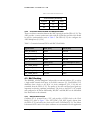
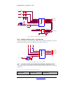
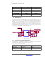
1
THE DINI GROUP LOGIC Emulation Source User Manual DNMEG_AD-DA LOGIC EMULATION SOURCE DNMEG_AD-DA User Manual Version 2.0 The Dini Group 7469 Draper Avenue La Jolla, CA92037 Phone 858.454.3419 • Fax 858.454.1728 [email protected] www.dinigroup.com Copyright Notice and Proprietary Information Copyright © 2006 The Dini Group. All rights reserved. No part of this copyrighted work may be reproduced, modified or distributed in any form or by any means, without the prior written permission of The Dini Group. Right to Copy Documentation The Dini Group permits licensee to make copies of the documentation for its internal use only. Each copy shall include all copyrights, trademarks, disclaimers and proprietary rights notices. Disclaimer The Dini Group has made reasonable efforts to ensure that the information in this document is accurate and complete. However, The Dini Group assumes no liability for errors, or for any incidental, consequential, indirect, or special damages, including, without limitation, loss of use, loss or alteration of data, delays, or lost profits or savings, arising from the use of this document or the product which it accompanies. Table of Contents INTRODUCTION ..................................................................................................................................................................................................................... 1 1 2 3 4 5 ABOUT THE DNMEG_AD-DA DAUGHTER CARD ......................................................................................................................................... 1 DNMEG_AD-DA DAUGHTER CARD FEATURES ........................................................................................................................................... 1 PACKAGE CONTENTS: ..................................................................................................................................................................................... 3 INSPECT THE BOARD ....................................................................................................................................................................................... 3 ADDITIONAL INFORMATION ............................................................................................................................................................................ 4 GETTING STARTED .............................................................................................................................................................................................................. 5 1 2 2.1 2.2 2.3 ESD WARNING ................................................................................................................................................................................................ 5 USING THE REFERENCE DESIGN (MAIN) ......................................................................................................................................................... 5 HyperTerminal Setup .............................................................................................................................................................................................. 6 Configuring the FPGA ............................................................................................................................................................................................ 7 Running the Reference Design ................................................................................................................................................................................ 9 HARDWARE DESCRIPTION .............................................................................................................................................................................................. 12 1 2 OVERVIEW ..................................................................................................................................................................................................... 12 XILINX VIRTEX-4 FPGA ............................................................................................................................................................................... 13 2.1 Summary of Virtex-4 Family Features: ................................................................................................................................................................ 14 3 FPGA CONFIGURATION ................................................................................................................................................................................ 15 3.1 Master Serial Configuration ................................................................................................................................................................................. 16 3.2 Boundary-Scan and JTAG Configuration............................................................................................................................................................. 16 3.2.1 In-System Programming PROM/JTAG Header ........................................................................................................................................... 17 3.2.2 JTAG connections to the PROM/FPGA ....................................................................................................................................................... 17 4 CLOCK GENERATION ..................................................................................................................................................................................... 18 4.1 Clock Methodology ............................................................................................................................................................................................... 18 4.2 ADC Clocking ....................................................................................................................................................................................................... 20 4.2.1 ADC Oscillator Circuit ................................................................................................................................................................................. 20 4.2.2 External ADC Clock Circuit ......................................................................................................................................................................... 20 4.2.3 Connection between FPGA and ADC Clock Buffer .................................................................................................................................... 21 4.3 DAC Clocking ....................................................................................................................................................................................................... 21 4.3.1 DAC Oscillator Circuit ................................................................................................................................................................................. 21 4.3.2 External DAC Clock Circuit ......................................................................................................................................................................... 22 4.3.3 Connection between FPGA and DAC Clock Buffer .................................................................................................................................... 23 4.4 DDR2 Clocking ..................................................................................................................................................................................................... 23 4.4.1 DDR2 Differential Oscillator Circuit ........................................................................................................................................................... 23 4.4.2 Connections between FPGA and the DDR2 Differential Oscillator ............................................................................................................ 23 4.4.3 DDR2 Differential Clock Buffer .................................................................................................................................................................. 24 4.4.4 Clocking Connections between DDR2 Clock Buffer and the SODIMM .................................................................................................... 24 4.5 Clock Synthesizer .................................................................................................................................................................................................. 25 4.5.1 Clock Synthesizer Circuit ............................................................................................................................................................................. 25 4.5.2 Connections between FPGA and the Clock Synthesizer .............................................................................................................................. 25 4.6 Daughter Card Clocks .......................................................................................................................................................................................... 26 4.6.1 Daughter Card Clock Circuit – Bottom Header (P3) ................................................................................................................................... 26 4.6.2 Daughter Card Clock Circuit – Top Header (P2) ......................................................................................................................................... 27 4.6.3 Connections between the FPGA and the Daughter Card Header Clocks..................................................................................................... 27 5 ANALOG TO DIGITAL CONVERTER (ADC) .................................................................................................................................................... 28 5.1 Differential Input ADC Driver .............................................................................................................................................................................. 29 5.1.1 Single-Ended Input Mode ............................................................................................................................................................................. 29 5.1.2 Differential Input Mode ................................................................................................................................................................................ 30 5.1.3 Gain Adjustment ........................................................................................................................................................................................... 30 5.1.4 Common-Mode Adjustment ......................................................................................................................................................................... 30 5.2 ADC ....................................................................................................................................................................................................................... 31 5.2.1 Clock Source ................................................................................................................................................................................................. 31 5.2.2 Analog Inputs ................................................................................................................................................................................................ 31 5.2.3 Voltage Reference ......................................................................................................................................................................................... 31 5.2.4 Data Format ................................................................................................................................................................................................... 31 5.2.5 Data Outputs .................................................................................................................................................................................................. 31 5.2.6 ADC Power Dissipation ................................................................................................................................................................................ 31 5.2.7 ADC Characterization ................................................................................................................................................................................... 31 5.2.8 ADC connections to the FPGA ..................................................................................................................................................................... 32 6 DIGITAL TO ANALOG CONVERTER (DAC) .................................................................................................................................................... 34 6.1 Clock Source ......................................................................................................................................................................................................... 34 6.2 Data Input.............................................................................................................................................................................................................. 35 6.3 DAC Differential Outputs ..................................................................................................................................................................................... 35 6.4 Voltage Reference ................................................................................................................................................................................................. 36 6.5 Full Scale Current Adjust ..................................................................................................................................................................................... 36 6.6 Serial Port Interface (SPI) .................................................................................................................................................................................... 36 6.7 DAC connections to FPGA ................................................................................................................................................................................... 36 7 MEMORY........................................................................................................................................................................................................ 38 7.1 Serial FLASH ........................................................................................................................................................................................................ 38 7.1.1 Connections between FPGA and Serial FLASH .......................................................................................................................................... 38 7.2 DDR2 SDRAM....................................................................................................................................................................................................... 39 7.2.1 DDR2 Clocking ............................................................................................................................................................................................. 39 7.2.2 DDR2 Termination Scheme .......................................................................................................................................................................... 39 7.2.3 Digitally Controlled Impedance (DCI) ......................................................................................................................................................... 41 7.2.4 On-Die Termination (ODT) .......................................................................................................................................................................... 41 7.2.5 VDD Switching Power Supply ....................................................................................................................................................................... 41 7.2.6 VTT Linear Power Supply ............................................................................................................................................................................ 42 7.2.7 Serial Presence-Detect Operation ................................................................................................................................................................. 42 7.2.8 JTAG connections to FPGA ......................................................................................................................................................................... 43 7.2.9 PCB Trace Lengths ....................................................................................................................................................................................... 47 8 LED INDICATORS .......................................................................................................................................................................................... 47 8.1 User LED’s ............................................................................................................................................................................................................ 47 8.2 Configuration DONE LED.................................................................................................................................................................................... 48 8.3 Power Supply Status LED’s .................................................................................................................................................................................. 48 9 RS232 PORT .................................................................................................................................................................................................. 49 9.1.1 Connections between FPGA and RS232 Port .............................................................................................................................................. 49 10 POWER DISTRIBUTION ................................................................................................................................................................................... 50 10.1 In-System Operation.......................................................................................................................................................................................... 50 10.2 Stand Alone Operation ...................................................................................................................................................................................... 50 10.2.1 External Power Connector ............................................................................................................................................................................ 51 11 DAUGHTER CARD HEADERS ......................................................................................................................................................................... 52 11.1 Daughter Card clocking.................................................................................................................................................................................... 52 11.2 Daughter Card Header Pin Assignments ......................................................................................................................................................... 52 11.2.1 Special Pins on the Daughter Card Header ................................................................................................................................................... 55 VREF ................................................................................................................................................................................................................................ 55 11.3 VCCO Power Supply ............................................................................................................................................................................................ 55 11.4 FPGA to Daughter Card Header IO Connections ........................................................................................................................................... 56 11.5 Power and Reset ................................................................................................................................................................................................ 62 11.6 Insertion/Removal of Daughter Card ............................................................................................................................................................... 63 11.7 MEG Array Specifications ................................................................................................................................................................................ 65 12 MICTOR HEADER ........................................................................................................................................................................................... 66 12.1.1 Mictor Header Circuit ................................................................................................................................................................................... 66 12.2 FPGA to Mictor Connections ........................................................................................................................................................................... 66 13 MECHANICAL ................................................................................................................................................................................................ 68 13.1 Dimensions ........................................................................................................................................................................................................ 68 APPENDIX 14 69 APPENDIX A: UCF FILE ................................................................................................................................................................................ 69 List of Figures Figure 1 - DNMEG_AD-DA Daughter Card ...................................................................................................................................................................................................... 1 Figure 2 - DNMEG_AD-DA Daughter Card Block Diagram ........................................................................................................................................................................ 13 Figure 3 - JTAG Header.......................................................................................................................................................................................................................................... 17 Figure 4 - Clocking Block Diagram ....................................................................................................................................................................................................................... 18 Figure 5 - ADC Oscillator Circuit ......................................................................................................................................................................................................................... 20 Figure 6 – External ADC Clock Circuit ............................................................................................................................................................................................................... 20 Figure 7 - DAC Oscillator Circuit ......................................................................................................................................................................................................................... 22 Figure 8 – External DAC Clock Circuit ............................................................................................................................................................................................................... 22 Figure 9 – DDR2 Differential Oscillator Circuit ................................................................................................................................................................................................ 23 Figure 10 – DDR2 Write PLL Circuit .................................................................................................................................................................................................................. 24 Figure 11 – Clock Synthesizer Circuit ................................................................................................................................................................................................................... 25 Figure 12 - Daughter Card Header Clock Circuit, Bottom Header ................................................................................................................................................................. 27 Figure 13 - Daughter Card Clock Circuit, Top Header ..................................................................................................................................................................................... 27 Figure 14 - Differential Input Amplifier ............................................................................................................................................................................................................... 29 Figure 15 – Single-Ended Input ............................................................................................................................................................................................................................. 30 Figure 16 - Differential Input ................................................................................................................................................................................................................................. 30 Figure 17 - FFT of the ADC Output .................................................................................................................................................................................................................... 32 Figure 18 – DAC Channel 1 Single-Ended Output............................................................................................................................................................................................ 36 Figure 19 - Serial FLASH ........................................................................................................................................................................................................................................ 38 Figure 20 - SSTL_18 Symmetrically Single Parallel Terminated ...................................................................................................................................................................... 40 Figure 21 - Symmetrically Double Parallel Terminated ..................................................................................................................................................................................... 41 Figure 22 - VDD Switching Power Supply .......................................................................................................................................................................................................... 42 Figure 23 - VTT Linear Power Supply ................................................................................................................................................................................................................. 42 Figure 24 - RS232 Port ............................................................................................................................................................................................................................................ 49 Figure 25 – In-System Daughter Card Header Power ....................................................................................................................................................................................... 50 Figure 26 - ATX Power Supply.............................................................................................................................................................................................................................. 51 Figure 27 - External Power Connection ............................................................................................................................................................................................................... 52 Figure 28 - Daughter Card Interconnect Diagram ............................................................................................................................................................................................. 53 Figure 29 - Daughter Card Header Pin Assignments ......................................................................................................................................................................................... 54 Figure 30 - VREF Signals........................................................................................................................................................................................................................................ 55 Figure 31 - VCCO Adjustable Linear Power Supplies ....................................................................................................................................................................................... 56 Figure 32 - Daughter Card Header Power & RESET ........................................................................................................................................................................................ 62 Figure 33 - 38 Pin Mictor Connector .................................................................................................................................................................................................................... 66 List of Tables Table 1 – Virtex-4 Uncompressed .rbf File Size ................................................................................................................................................................................................. 16 Table 2 - JTAG connections to the PROM/FPGA ........................................................................................................................................................................................... 17 Table 3 - Clocking to/from the FPGA ................................................................................................................................................................................................................. 18 Table 4 - External ADC Clock Interface Levels ................................................................................................................................................................................................. 21 Table 5 - Connection between FPGA and ADC Clock Buffer ........................................................................................................................................................................ 21 Table 6 - External DAC Clock Interface Levels ................................................................................................................................................................................................. 22 Table 7 - Connection between FPGA and DAC Clock Buffer ........................................................................................................................................................................ 23 Table 8 - Connections between FPGA and the DDR2 Differential Oscillator ............................................................................................................................................. 24 Table 9 - Connections between FPGA and the DDR2 Differential Clock Buffer ....................................................................................................................................... 25 Table 10 - Connections between FPGA and Clock Synthesizer ...................................................................................................................................................................... 26 Table 11 - Connections between FPGA and Daughter Card Header Clocks ................................................................................................................................................ 27 Table 12 - ADC Migration ...................................................................................................................................................................................................................................... 28 Table 13- ADC Connections to the FPGA ......................................................................................................................................................................................................... 32 Table 14- DAC Connections to the FPGA ......................................................................................................................................................................................................... 37 Table 15 - Connections between FPGA and the Serial FLASH ...................................................................................................................................................................... 39 Table 16 - DDR2 Termination Scheme ................................................................................................................................................................................................................ 40 Table 17 - Serial Presence-Detect Connections .................................................................................................................................................................................................. 43 Table 18 - Connections between the FPGA and the DDR2 SODIMM ........................................................................................................................................................ 43 Table 19 – PCB Trace Lengths .............................................................................................................................................................................................................................. 47 Table 20 – User LED’s ............................................................................................................................................................................................................................................ 48 Table 21 – DONE LED ......................................................................................................................................................................................................................................... 48 Table 22 – Power Supply Status LED’s ................................................................................................................................................................................................................ 48 Table 23 - Connections between FPGA and the RS232 Port........................................................................................................................................................................... 49 Table 24 - FPGA to Daughter Card Header IO Connections ......................................................................................................................................................................... 56 Table 25 – Daughter Card Reset Signal (DC_RSTn) ......................................................................................................................................................................................... 63 Table 26 - Connections between FPGA and Mictor Connector ...................................................................................................................................................................... 67 1 Chapter I N T R O D U C T I O N Introduction This User Manual accompanies the DNMEG_AD-DA Daughter Card. For specific information regarding the Virtex-4 parts, please reference the datasheet on the Xilinx website. 1 About the DNMEG_AD-DA Daughter Card The DNMEG_AD-DA Daughter Card provides a complete development platform for designing and verifying DSP applications based on the Xilinx Virtex-4 FPGA family. The DNMEG_AD-DA provides dual 12-Bit/210 MSPS independent ADC channels and a dual 16-Bit/160 MSPS DAC. The DNMEG_AD-DA Daughter Card can operate in standalone mode or in conjunction with one of the Dini products that houses a 400 pin MEG-Array Daughter card header, e.g. DN8000K10PSX. 2 DNMEG_AD-DA Daughter Card Features Figure 1 - DNMEG_AD-DA Daughter Card DNMEG_AD-DA Daughter Card features the following: Single Xilinx Virtex-4 FPGA (FF1148) DNMEG_AD-DA User Manual www.dinigroup.com 1 I N T R O D U C T I O N o XC4VLX40/60/80/100/160 -10, -11, -12 o XC4VSX55 -10, -11, -12 Analog to Digital Converter (ADC) o 12-Bit/210 MSPS A/D Converter AD9430-210 (x2) Digital to Analog (DAC) o 16-Bit/160 MSPS Interpolating Dual TxDAC D/A Converter Various clock sources: o ADC/DAC External Clock Inputs o ADC/DAC Clock Oscillators o DDR2 Oscillator (x1) o FPGA Clock Synthesizer (x1) o Multiple clocks from the Daughter Card Headers Memory o DDR2, 512MB (32MB x 64 Bit), 200MHz SODIMM (PC2-3200), support up to 2GB o Serial FLASH Memory, 4Mbit (2048 pages of 264 bytes per page) Status LED’s (x8) Daughter Card Headers (x2) LVDS – MEG-Array (400 pin) interface to DN7000K10xxx/DN8000K10xxx products Onboard distributed Power Supplies Full support for embedded Logic Analyzers o ChipScopeTM from Xilinx o IdentifyTM from Synplicity o Mictor Interface (38 Pin) DNMEG_AD-DA User Manual www.dinigroup.com 2 I N T R O D U C T I O N RS232 Port – MicroBlaze FPGA Configuration via Xilinx Platform Cable USB Stand Alone operation, requires an external +5V/+12V power supply (ATX) 3 Package Contents: Before using the kit or installing the software, be sure to check the contents of the kit and inspect the board to verify that you received all of the items. If any of these items are missing, contact The Dini Group before you proceed. The DNMEG_AD-DA Daughter Card kit includes the following: RS232 IDC header cable to female DB9 RS232 serial cable (DB9) CD ROM containing: o Virtex-4 Reference Design (Verilog) o User manual (pdf format) o Board Schematic (pdf format) o Component Datasheets (pdf format) Optional items that support development efforts (not provided): Xilinx ISE software Xilinx Platform Cable USB download cable DDR-II SODIMM (Available upon request) 4 Inspect the Board Place the board on an anti-static surface and inspect it to ensure that it has not been damaged during shipment. Verify that all components are on the board and appear intact. DNMEG_AD-DA User Manual www.dinigroup.com 3 I N T R O D U C T I O N 5 Additional Information For additional information, please visit http://www.dinigroup.com/. The following table lists some of the resources you can access from this website. You can also directly access these resources using the provided URLs. Resource User Manual Description/URL This is the main source of technical information. The manual should contain most of the answers to your questions Demonstration Videos MEG-Array Daughter Card header insertion and removal video Dini Group Web Site The web page will contain the latest user manual, application notes, FAQ, articles, and any device errata and manual addenda. Please visit and bookmark: http://www.dinigroup.com Data Book Pages from Virtex-4 Databook, which contains devicespecific information on Xilinx device characteristics E-Mail You may direct questions and feedback to the Dini Group using this e-mail address: [email protected] Phone Support Call us at 858.454.3419 during the hours of 8:00am to 5:00pm Pacific Time. FAQ The download section of the web page may contain a document called DNMEG_AD-DA Frequently Asked Questions (FAQ). This document is periodically updated with information that may not be in the Users Manual. DNMEG_AD-DA User Manual www.dinigroup.com 4 G E T T I N G 2 Chapter S T A R T E D Getting Started Congratulations on your purchase of the DNMEG_AD-DA Daughter Card. The remainder of this chapter describes the contents of the box and how to run the reference design that accompanies the DNMEG_AD-DA Daughter Card. 1 ESD Warning The DNMEG_AD-DA Daughter Card is sensitive to static electricity, so treat the PCB accordingly. The target markets for this product are engineers that are familiar with FPGAs and circuit boards. However, if needed, the following web page has an excellent tutorial on the “Fundamentals of ESD” for those of you who are new to ESD sensitive products: http://www.esda.org/basics/part1.cfm The DNMEG_AD-DA Daughter Card has been factory tested and pre-programmed to ensure correct operation. You do not need to alter any jumpers or program anything to see the board work. A reference design is included on the CD provided. The 400pin daughter card connectors are not 5V tolerant. Take care when handling the board to avoid touching the daughter card connectors. 2 Using the Reference Design (Main) The Dini Group provides a reference design for the DNMEG_AD-DA to help the user get familiar with the board and start building applications: MainRef – Described in this document, programs the PROM with a design that configures the FPGA and allows the user to test all the interfaces on the board. DNMEG_AD-DA User Manual www.dinigroup.com 5 G E T T I N G S T A R T E D Attach an ATX Power Supply to the power header (J12) on the DNMEG_AD-DA Daughter Card. Connect the “Xilinx Platform Cable USB” from the Test PC to the JTAG Header (J13). Connect the RS232 serial cable from the Test PC to the RS232 Header (P1). Ensure that pin 1 location of the cable aligns with pin 1 location on the PCB. If the kit contains a Memory Module, populate J14 with the SODIMM Module. Do not insert the SODIMM module with the board powered. 2.1 HyperTerminal Setup Connect the RS232 Serial cable to a COM port on the Test PC and configure HyperTerminal to the following settings: DNMEG_AD-DA User Manual www.dinigroup.com 6 G E T T I N G S T A R T E D 2.2 Configuring the FPGA This section lists detailed instructions for programming the Xilinx Virtex-4 FPGA using the Xilinx ISE Version 9.1.03i tools. Ensure the “Xilinx Platform Cable USB” is connected to the “JTAG” header (J13) on the DNMEG_AD-DA Daughter Card. Power the DNMEG_AD-DA daughter card and verify that the Power LEDs (DS12, DS11, DS14, DS13) are ON. Note: This User Manual will not be updated for every revision of the Xilinx tools, so please be aware of minor differences. 1. Open iMPACT and create a new default project. Select “Configure devices using Boundary-Scan (JTAG)” from the iMPACT welcome menu. DNMEG_AD-DA User Manual www.dinigroup.com 7 G E T T I N G S T A R T E D 2. iMPACT will identify the devices in the JTAG chain. Specify the file location for the PROM programming file based on the type of FPGA populated e.g. XC4VLX40, “CUST_CD\DN_BITFILES\DNMEG_ADDA\MainRef\LX40” and open the PROM file “prom_xcf32.mcs”. Note: The FPGA will be high-lighted in the JTAG chain, select Bypass since we intend to configure the FPGA with the PROM. 3. Right-click on the XCF32P device and select “Program”. Click “OK” to program the PROM. A Process Dialog box will indicate programming progress. DNMEG_AD-DA User Manual www.dinigroup.com 8 G E T T I N G S T A R T E D 4. Power-cycle the DNMEG_AD-DA Daughter Card and verify that the “FPGA DONE” blue LED (DS9) is enabled, indicating successful configuration of the FPGA. 2.3 Running the Reference Design This section lists detailed instructions for executing the reference design. After configuring the FPGA, perform the following steps; 1. Press “ENTER” in the HyperTerminal window to display the “DNMEG_AD-DA Main Menu”. DNMEG_AD-DA User Manual www.dinigroup.com 9 G E T T I N G S T A R T E D 2. Select test option a, “DDR2 Test” in the HyperTerminal window and verify that the test PASS (periods will be displayed as the memory locations are being tested, if no DDR2 Module is present, the test will display read/write errors). Press “ENTER” to stop the test. 3. Select test option b, “SPI FLASH Test” in the HyperTerminal window and verify that the test PASSED. DNMEG_AD-DA User Manual www.dinigroup.com 10 G E T T I N G S T A R T E D 4. Connect a Signal Generator (1MHz Sine Wave, 200mVptp, 0V Offset) to the ADC channel 0 SMA (J1). Select test option c, “ADC0 Start Capture (1K)” in the HyperTerminal window and verify that the digital data captured increments/decrements to the amplitude of a sine wave. 5. Connect a Signal Generator (1MHz Sine Wave, 500mVptp, 0V Offset) to the ADC channel 1 SMA (J3). Select test option d, “ADC1 Start Capture” in the HyperTerminal window and verify that the data captured increments/decrements to the amplitude of a sine wave. 6. Connect an Oscilloscope to the DAC channel 1 SMA (J5). Select test option v, “DAC Menu” in the HyperTerminal window and verify that the data output is a sinusoidal waveform. Please reference the CUST CD for code examples. The next section describes the hardware in detail. DNMEG_AD-DA User Manual www.dinigroup.com 11 H A R D W A R E 3 Chapter D E S C R I P T I O N Hardware Description This chapter describes the functional blocks of the design and focuses on the Hardware implementation. 1 Overview The DNMEG_AD-DA Daughter Card provides for a comprehensive collection of peripherals to use in creating a system around the Xilinx Virtex-4 FPGA. A high level block diagram of the DNMEG_AD-DA Daughter Card is shown in Figure 2, followed by a brief description of each section. DNMEG_AD-DA User Manual www.dinigroup.com 12 H A R D W A R E D E S C R I P T I O N EXT POWER SWITCHING PSU +5V 1.8V @ 5A PTH05050W +12V LED7 LED6 LED5 LED3 LED4 LED2 LED1 LED0 STATUS LED'S LINEAR PSU 0.9V @ 1.5A LP2996 DDR-II SODIMM 2GB (200PIN) CHANNEL 1 A/D CONVERTER 12-Bit 210MSPS AD9430 A/D CONVERTER 12-Bit 210MSPS AD9430 CHANNEL 1 A1 A34 6 1 9 14 VIRTEX-4 FPGA 13 CONFIGURATION PROM XCF32P SERIALFLASH 4 Mbit AT45DB041B +3.3V @ 6A +12V @ 4A +5V @ 4A JTAG RS232 FPGA Options: LX40* LX60* LX80 LX100 LX160 SX55* * NC on Bank 2 of the Daughter Card Headers (IO Bank 13 not available) PSU 1.2V @ 10A YNS05S10 DAUGHTER CARD AP34 MEG ARRAY – Receptacle (400Pin) – Bottom 74390-101LF AP1 11 7 DAUGHTER CARD 4 8 CLOCK CIRCUIT MEG ARRAY – 400PIN - Top 84520-102LF XC4VSX55 (FBGA1148) 2 12 CHANNEL 2 5 3 10 CHANNEL 2 DAC CONVERTER 16-Bit 400MSPS AD9777 EXT CLOCK MICTOR PSU 2.5V @ 5A PTH05050W PSU 3.3V @ 5A PTH05050W Figure 2 - DNMEG_AD-DA Daughter Card Block Diagram 2 Xilinx Virtex-4 FPGA The Virtex-4 Family is the newest generation FPGA from Xilinx. The innovative Advanced Silicon Modular Block or ASMBL column-based architecture is unique in the programmable logic industry. Virtex-4 FPGAs contain three families (platforms): LX, FX, and SX. Choice and feature combinations are offered for all complex applications. A wide array of hard-IP core blocks completes the system solution. These cores include the PowerPC processors (with a new APU interface), Tri-mode Ethernet MACs, 622 Mb/s to 6.5 Gb/s serial transceivers, dedicated DSP slices, high-speed clock management circuitry, and source-synchronous interface blocks. The basic Virtex-4 building blocks are an enhancement of those found in the popular Virtexbased product families: Virtex, Virtex-E, Virtex-II, Virtex-II Pro, and Virtex-II Pro X, allowing upward compatibility of existing designs. Virtex-4 devices are produced on a state-of-the-art 90-nm copper process using 300-mm (12-inch) wafer technology. Combining a wide variety of flexible features, the Virtex-4 family enhances programmable logic design capabilities and is a powerful alternative to ASIC technology. DNMEG_AD-DA User Manual www.dinigroup.com 13 H A R D W A R E D E S C R I P T I O N 2.1 Summary of Virtex-4 Family Features: Three Families - LX/SX/FX o Virtex-4 LX: High-performance logic applications solution o Virtex-4 SX: High-performance solution for digital signal processing (DSP) applications o Virtex-4 FX: High-performance, full-featured solution for embedded platform applications Xesium Clock Technology o Digital clock manager (DCM) blocks o Additional phase-matched clock dividers (PMCD) o Differential global clocks XtremeDSP Slice o 18 x 18, two’s complement, signed Multiplier o Optional pipeline stages o Built-in Accumulator (48-bit) and Adder/Subtracter Smart RAM Memory Hierarchy o Distributed RAM o Dual-port 18-Kbit RAM blocks o Optional pipeline stages o Optional programmable FIFO logic automatically remaps RAM signals as FIFO signals o High-speed memory interface supports DDR and DDR-2 SDRAM, QDR-II, and RLDRAM-II. SelectIOTechnology o 1.5V to 3.3V I/O operation o Built-in ChipSync source-synchronous technology DNMEG_AD-DA User Manual www.dinigroup.com 14 H A R D W A R E D E S C R I P T I O N o Digitally controlled impedance (DCI) active termination o Fine grained I/O banking (configuration in one bank) Flexible Logic Resources Secure Chip AES Bitstream Encryption 90-nm Copper CMOS Process 1.2V Core Voltage Flip-Chip Packaging including Pb-Free Package Choices RocketIO 622 Mb/s to 6.5 Gb/s Multi-Gigabit Transceiver (MGT) [FX only] IBM PowerPC RISC Processor Core [FX only] o PowerPC 405 (PPC405) Core o Auxiliary Processor Unit Interface (User Coprocessor) Multiple Tri-Mode Ethernet MACs [FX only] 3 FPGA Configuration Virtex-4 devices are configured by loading application-specific configuration data - the bitstream - into internal memory. Because Xilinx FPGA configuration memory is volatile, it must be configured each time it is powered-up. The bitstream is loaded into the device through special configuration pins. These configuration pins serve as the interface for a number of different configuration modes: Master-serial configuration mode Slave-serial configuration mode Master SelectMAP (parallel) configuration mode Slave SelectMAP (parallel) configuration mode In addition, the bitstream can be loaded through the JTAG interface: JTAG/Boundary-scan configuration mode DNMEG_AD-DA User Manual www.dinigroup.com 15 H A R D W A R E D E S C R I P T I O N The configuration mode is selected by setting the appropriate level on the dedicated configuration MODE pins. The DNMEG_AD-DA Daughter Card supports Master Serial and JTAG configuration modes. The JTAG/Boundary-scan configuration interface is always available, regardless of the MODE pin settings. The JTAG/Boundary-scan configuration mode disables all other configuration modes. This prevents conflicts between configuration interfaces. 3.1 Master Serial Configuration When the FPGA is in the Master Serial mode, it generates a configuration clock that drives the configuration PROM. These configuration devices are low-cost devices with non-volatile memory that feature a simple four-pin interface and a small form factor. These features make serial configuration devices an ideal low-cost configuration solution. Serial configuration devices provide a serial interface to access configuration data. During device configuration, Virtex-4 devices read configuration data via the serial interface, and configure their SRAM cells. This scheme is referred to as the Master Serial configuration scheme because the Virtex-4 FPGA (U15) controls the configuration interface. The XCF32P (U27) serial configuration PROM support CCLK up to 33MHz. Table 1 shows the uncompressed configuration file size for the largest Virtex-4 devices that are supported and configured by the PROM. Table 1 – Virtex-4 Uncompressed .rbf File Size Device Data Size (Bits) XC4VLX100 30,711,680 XC4VSX55 22,749,184 3.2 Boundary-Scan and JTAG Configuration Virtex-4 devices support the new IEEE 1532 standard for In-System Configuration (ISC), based on the IEEE 1149.1 standard. The IEEE 1149.1 Test Access Port and Boundary-Scan Architecture is commonly referred to as JTAG. JTAG is an acronym for the Joint Test Action Group, the technical subcommittee initially responsible for developing the standard. This standard provides a means to ensure the integrity of individual components and the interconnections between them at the board level. With multi-layer PC boards becoming increasingly dense and more sophisticated surface mounting techniques in use, boundary scan testing is becoming widely used as an important debugging standard. The Virtex-4 family is fully compliant with the IEEE Standard 1149.1 Test Access Port and Boundary-Scan Architecture. The architecture includes all mandatory elements defined in the IEEE 1149.1 Standard. These elements include the Test Access Port (TAP), the TAP controller, the instruction register, the instruction decoder, the boundary-scan register, and the bypass register. The Virtex-4 family also supports a 32bit identification register and a configuration register in full compliance with the DNMEG_AD-DA User Manual www.dinigroup.com 16 H A R D W A R E D E S C R I P T I O N standard. A device operating in JTAG mode uses four required pins, TDI, TDO, TMS, and TCK. The four JTAG input pins (TDI, TMS, TCK and TRST) have weak, internal pull-up resistors. Do not begin JTAG configuration until all other configuration is complete. 3.2.1 In-System Programming PROM/JTAG Header In-System Programming is possible by daisy-chaining the PROM and the FPGA. Figure 3 shows the pin assignments for the JTAG programming header. +3.3V +3.3V C177 10uF 16V 20% CERAMIC C176 0.1uF R273 1K J13 1 3 5 7 9 11 13 R271 1K 2 4 6 8 10 12 14 R270 1K JTAG_PROM_TMS JTAG_PROM_TCK JTAG_PROM_TDO JTAG_PROM_TDI R272 1K 87832-1420 Figure 3 - JTAG Header 3.2.2 JTAG connections to the PROM/FPGA Table 2 shows the connection between the JTAG connector and the Configuration PROM/Virtex-4 FPGA. Table 2 - JTAG connections to the PROM/FPGA Signal Name PROM Pin (Name) Connector JTAG_PROM_TMS U27.21 (TMS) J13.4 JTAG_PROM_TCK U27.20 (TCK) J13.6 JTAG_PROM_TDO U27.22 (TDO) J13.8 JTAG_PROM_TDI U27.19 (TDI) J13.10 FPGA Pin (Name) Connector JTAG_PROM_TMS U15.V13 (TMS) J13.4 JTAG_PROM_TCK U15.V14 (TCK) J13.6 JTAG_PROM_TDO U15.V18 (TDO) J13.8 JTAG_PROM_TDI U15.W17 (TDI) J13.10 Signal Name DNMEG_AD-DA User Manual www.dinigroup.com 17 H A R D W A R E D E S C R I P T I O N 4 Clock Generation 4.1 Clock Methodology The DNMEG_AD-DA has a flexible and configurable clocking scheme. Figure 4 is a block diagram showing the clocking resources and connections. EXT CLK ADC OSC (LVDS) (5x7) CLK0_EXT_ADC0p/n CLK_ADC0p/n CLK1_EXT_ADC1p/n ADC EXT/ USER CLK BUFFER ADC0 CLK2_EXT_ADC1p/n_180 ADC0_DCLKOUTp/n AD9430 MUX ICS854054 CLK_FPGA_ADC0p/n ICS85214 CLK3_EXT_DAC0p/n CLK_ADC1p/n ADC1 ADC1_DCLKOUTp/n AD9430 CLK_FPGA_ADC1p/n MUX ICS854054 EXT CLK EXT CLK CLK0_EXT_DAC1p/n DAC OSC (LVDS) (5x7) DAC EXT/ USER CLK BUFFER CLK_MUX_DACp/n DAC MUX AD9777 ICS85411 MUX CLK2_EXT_DACp/n ICS854054 ICS85214 CLK1_EXT_DAC1p/n CLK_FPGA_DACp/n DC_B0p/n31 DDR2_CK0p/n DC_B0p/n31 CLK_DC_FPGAp/n MEG ARRAY – 400Pin 84520-102LF DAUGHTER CARD DAUGHTER CARD MEG ARRAY – Receptacle (400Pin) 74390-101LF LVDS BUFFER ICS85411 (SO8) DDR2_CK1p/n CLK_DC_B_2p/n DDR-II SODIMM 2GB (200PIN) Virtex-4 FPGA XC4VLX40 CLK_DC_B_0p/n DDR2_OSC_OUTp/n LVDS OSC DDR2 (EG2121) CLK_DC_B_1p/n CLK_SYNTH0p/n CLK_DC_T_2p/n CLK_SYNTH1p/n Clock Synthesizer ICS8442 (LQFP32) Figure 4 - Clocking Block Diagram The clocking structures for the DNMEG_AD-DA include the following features: ADC/DAC External Clock Inputs (J7, J9) ADC/DAC Clock Oscillators (X1, X2) DDR2 Oscillator (U16) FPGA Clock Synthesizer (U21) Multiple clocks from the Daughter Card Headers (P2, P3) The connections between the FPGA and various clocking resources are documented in Table 3, covering the clocking inputs and outputs, respectively. Table 3 - Clocking to/from the FPGA DNMEG_AD-DA User Manual www.dinigroup.com 18 H A R D W A R E D E S C R I P T I O N Signal Name Clock Buffer (Pin) FPGA (Pin) CLK_DAC_FPGAp U24-3 U15-AG18 CLK_DAC_FPGAn U24-4 U15-AG17 Signal Name FPGA (Pin) Clock Buffer (Pin) CLK_FPGA_DACp U15-AF5 U12-1 CLK_FPGA_DACn U15-AF4 U12-2 Signal Name FPGA (Pin) Clock Buffer (Pin) CLK_FPGA_ADC0p U15-C2 U9-1 CLK_FPGA_ADC0n U15-D2 U9-2 CLK_FPGA_ADC1p U15-P7 U10-1 CLK_FPGA_ADC1n U15-P6 U10-2 Signal Name Clock Buffer (Pin) FPGA (Pin) CLK_DC_FPGAp U26-3 U15-AH19 CLK_DC_FPGAn U26-4 U15-AH18 Signal Name FPGA (Pin) DDR2 Clock Buffer (Pin) CLK_DDR2p U15-AM20 U23-4 CLK_DDR2n U15-AL19 U23-5 Signal Name DDR2 Clock Buffer (Pin) FPGA (Pin) CLK_DDR2_FBp U23-3 U15-AM17 CLK_DDR2_FBn U23-2 U15-AM16 Signal Name Daughter Card Header (Pin) FPGA (Pin) CLK_DC_B_0p P3-E1/ P2-E1 U15-AF18 CLK_DC_B_0n P3-F1/ P2-F1 U15-AE18 CLK_DC_B_1p P3-E3/ P2-E3 U15-AG16 CLK_DC_B_1n P3-F3/ P2-F3 U15-AF16 CLK_DC_T_2p P2-E5 U15-AK18 CLK_DC_T_2n P2-F5 U15-AK17 Signal Name Clock Synthesizer (Pin) FPGA (Pin) CLK_SYNTH0p U21-14 U15-M18 CLK_SYNTH0n U21-15 U15-L18 CLK_SYNTH1p U21-11 U15-AC19 CLK_SYNTH1n U21-12 U15-AB18 DNMEG_AD-DA User Manual www.dinigroup.com 19 H A R D W A R E D E S C R I P T I O N 4.2 ADC Clocking The DNMEG_AD-DA Daughter Card provides an onboard oscillator (X2) as well as a single-ended external clock input via an SMA connector (J7). Clock Buffer (U11) distributes these clocks to both ADC’s via clock Multiplexers (U9, U10) that are controlled from the FPGA (U15). Please refer to the schematic. 4.2.1 ADC Oscillator Circuit Oscillator (X2) is powered from +2.5V, and provides a LVDS clock to the Clock Buffer (U11), refer to Figure 5. The “EXT_ADC_CLK_SEL” signal is driven from the FPGA (U15) and selects the clock source on the Clock Buffer (U11). The Silicon Laboratories Si531 series of low jitter oscillators are recommended for this application and is available in 10.0MHz to 945MHz from Silicon Laboratories, part number: 531FB210M000BG (factory default, 210 MHz). +2.5V FB22 +2.5V VCC_OSC_ADC BLM18AG102SN1 100mA R108 1K C457 0.1uF X2 1 2 3 OE VCC NC OUT GND OUT 6 4 OSC_ADCp 5 OSC_ADCn 531FB210M000BG Figure 5 - ADC Oscillator Circuit 4.2.2 External ADC Clock Circuit The external clock input (J7) is AC-coupled (C204) and biased by R130 and R131, refer to Figure 6. J7 is an Amphenol SMA right-angle PCB mounted jack P/N 901-1448RFX with an impedance rating of 50Ω. +3.3V R130 100 J7 2 3 5 1 4 901-144-8RFX R107 EXT_ADC_CLK C204 0.1uF cEXT_ADC_CLK 5.1 R119 49.9 R131 100 Figure 6 – External ADC Clock Circuit External ADC Clock Interface Levels The external ADC clock input must conform to the interface levels as specified in the in the datasheet the Differential to HSTL Fanout Buffer ICS85214 (U11), see Table 4 below. The maximum input clock frequency is limited by the ADC to 210MHz. DNMEG_AD-DA User Manual www.dinigroup.com 20 H A R D W A R E D E S C R I P T I O N Table 4 - External ADC Clock Interface Levels Fanout Buffer (ICS85214) 4.2.3 Symbol Min Max VIH 2.0 3.6 VIL -0.3 1.3 Connection between FPGA and ADC Clock Buffer There is no direct connection between the ADC input clock and the FPGA (U15). The ADC provides a source synchronous clock with the LVDS data, and this clock should be used for synchronization, refer to Table 5. The FPGA (U15) also configures the ADC Multiplexers (U9, U10). Table 5 - Connection between FPGA and ADC Clock Buffer Signal Name ADC (Pin) FPGA (Pin) ADC0_DCLKOUTp U6-64 U15-K18 ADC0_DCLKOUTn U6-63 U15-K17 ADC1_DCLKOUTp U7-64 U15-K19 ADC1_DCLKOUTn U7-63 U15-J19 FPGA (Pin) Clock Multiplexer (Pin) CLK_FPGA_ADC0p U15-C2 U9-1 CLK_FPGA_ADC0n U15-D2 U9-2 CLK_FPGA_ADC1p U15-P7 U10-1 CLK_FPGA_ADC1n U15-P6 U10-2 4.3 DAC Clocking The DNMEG_AD-DA Daughter Card provides an onboard oscillator (X3) as well as a single-ended external clock input via an SMA connector (J9). Clock Buffer (U13) distributes these clocks to the DAC via clock multiplexer (U12, U24) that are controlled from the FPGA (U15). The quality of the clock and data input signals are important in achieving optimum performance. The clock to the DAC is AC-coupled and configured to be driven differentially; R22/R97 and R98/R23 set the differential bias. Please refer to the schematic. 4.3.1 DAC Oscillator Circuit Oscillator (X3) is powered from +2.5V, and provides a LVDS clock to the Clock Buffer (U13), refer to Figure 7. The “EXT_DAC_CLK_SEL” signal is driven from the FPGA (U15) and selects the clock source on the Clock Buffer (U13). The Silicon Laboratories Si531 series of low jitter oscillators are recommended for this application DNMEG_AD-DA User Manual www.dinigroup.com 21 H A R D W A R E D E S C R I P T I O N and is available in 10.0MHz to 945MHz from Silicon Laboratories, part number: 531FB160M000BG (factory default, 160 MHz). +2.5V +2.5V FB23 VCC_OSC_DAC BLM18AG102SN1 100mA R118 1K C458 0.1uF X3 1 2 3 OE VCC NC OUT GND OUT 6 4 OSC_DACp 5 OSC_DACn 530FB160M000BG Figure 7 - DAC Oscillator Circuit 4.3.2 External DAC Clock Circuit The external clock input (J9) is AC-coupled (C206) and biased by R137 and R138, refer to Figure 8. J7 is an Amphenol SMA right-angle PCB mounted jack P/N 901-1448RFX with an impedance rating of 50Ω. +3.3V R137 100 J9 2 3 R157 5 1 4 EXT_DAC_CLK C206 0.1uF cEXT_DAC_CLK 5.1 901-144-8RFX R159 49.9 R138 100 Figure 8 – External DAC Clock Circuit External DAC Clock Interface Levels The external DAC clock input must conform to the interface levels as specified in the in the datasheet the Differential to HSTL Fanout Buffer ICS85214 (U13), see Table 6 below. The maximum input clock frequency is limited by the DAC to 160MHz. Table 6 - External DAC Clock Interface Levels Fanout Buffer (ICS85214) Symbol Min Max VIH 2.0 3.6 VIL -0.3 1.3 DNMEG_AD-DA User Manual www.dinigroup.com 22 H A R D W A R E 4.3.3 D E S C R I P T I O N Connection between FPGA and DAC Clock Buffer The connection between the FPGA and the DAC Clock Buffer (U13) is shown in Table 7. Please note that the DAC clock will be delayed by the propagation delays through the Multiplexers (U12, U24). Table 7 - Connection between FPGA and DAC Clock Buffer Signal Name DAC Clock Buffer (Pin) FPGA (Pin) CLK1_EXT_DAC1p U13-3 U15-AB17 CLK1_EXT_DAC1n U13-4 U15-AB16 4.4 DDR2 Clocking The DDR2 SDRAM module (J14) uses the SSTL 1.8V I/O standard and uses DDR architecture to achieve high-speed operation. The memory operates using a differential clock provided by the controller. Commands are registered at every positive edge of the clock. A bidirectional data strobe (DQS) is transmitted along with the data for use in data capture at the receiver. DQS is transmitted by the DDR2 SDRAM device during reads, and the controller transmits DQS during writes. DQS is edge-aligned with data for reads and is center-aligned with data for writes. Refer to XAPP702 – DDR2 Controller Using Virte-4 Devices for more information regarding the data path architecture. 4.4.1 DDR2 Differential Oscillator Circuit The differential oscillator (U16) is powered from +2.5V, and provides a differential clock to the FPGA (U15), see Figure 9. The Epson EG2102CA Series of low jitter (0.2ps) LVDS oscillators is recommended for this application and is available in 53.125Hz to 700MHz. They are available from Nu Horizons, part number: EG2121CA200.0000M-LGPN. +2.5V FB19 VCC_OSC_DDR2 BLM18AG102SN1 100mA R172 1K C115 0.1uF U16 DDR2_OSC_OE 1 2 3 OE VCC NC OUT# GND OUT 6 5 DDR2_OSC_OUTn 4 DDR2_OSC_OUTp EG-2121CA 53.125MHz to 700MHz (200MHz Factory Default) Figure 9 – DDR2 Differential Oscillator Circuit 4.4.2 Connections between FPGA and the DDR2 Differential Oscillator The connections between the FPGA, the Differential Oscillator and the DDR2 Clock Buffer are shown in Table 8. DNMEG_AD-DA User Manual www.dinigroup.com 23 H A R D W A R E D E S C R I P T I O N Table 8 - Connections between FPGA and the DDR2 Differential Oscillator Signal Name DDR2 Diff OSC FPGA (Pin) DDR2_OSC_OUTp U4.4 U15.AN20 DDR2_OSC_OUTn U4.5 U15.AP20 Signal Name FPGA (Pin) DDR2 Clock Buffer (Pin) CLK_DDR2P U15-AM20 U23-4 CLK_DDR2N U15-AL19 U23-5 4.4.3 DDR2 Differential Clock Buffer The CDCU877 (U23) is a high-performance, low-jitter, low-skew, zero-delay buffer that distributes a differential clock input pair (CK, CK) to ten differential pairs of clock outputs (Yn, Yn) and to one differential pair of feedback clock outputs (FBOUT, FBOUT). The feedback clock “CLK_DDR2_FBp/n” is routed from the Clock Buffer (U23) to a clock input on the FPGA (U15) and is matched length to the data byte group. VTT_900mV R235 49.9 CLK_DDR2p C169 0.1uF CLK_DDR2n C168 0.1uF R234 49.9 U23 4 5 R230 CLK CLK Y0 Y0 100 27 26 Y1 Y1 FBIN FBIN Y2 Y2 Y3 Y3 +1.8V +1.8V +1.8V R54 1 R231 R232 DDR2_OS DDR2_OE 1K 1K FB21 VCCA_DDR2_FIL1V8 C163 BLM18AG102SN1 10uF C162 100mA 16V 0.1uF 20% CERAMIC Place 2200pF capacitor close to the PLL AVDD pin. 21 22 8 C161 2200pF 1 6 9 15 20 23 28 31 36 7 10 41 OS OE Y4 Y4 AVDD Y5 Y5 VDDQ VDDQ VDDQ VDDQ VDDQ VDDQ VDDQ VDDQ VDDQ Y6 Y6 Y7 Y7 Y8 Y8 Y9 Y9 AGND GND GND PAD FBOUT FBOUT 38 37 DDR2_CKp0 DDR2_CKn0 39 40 DDR2_CKp1 DDR2_CKn1 3 2 CLK_DDR2_FBp CLK_DDR2_FBn 11 12 14 13 34 35 33 32 29 30 19 18 16 17 24 25 CLK_DDR2_FBOUTp CLK_DDR2_FBOUTn CDCU877/QFN40 Figure 10 – DDR2 Write PLL Circuit 4.4.4 Clocking Connections between DDR2 Clock Buffer and the SODIMM The clocking connections between the DDR2 Clock Buffer (U23) SDRAM SODIMM (J14) are shown in Table 9. DNMEG_AD-DA User Manual www.dinigroup.com 24 H A R D W A R E D E S C R I P T I O N Table 9 - Connections between FPGA and the DDR2 Differential Clock Buffer Signal Name FPGA (Pin) DDR2 SODIMM DDR2_CKp0 U23-38 J14-30 DDR2_CKn0 U23-37 J14-32 DDR2_CKp0 U23-39 J14-164 DDR2_CKn0 U23-40 J14-166 CLK_DDR2_FBp U23-3 U15-AM17 CLK_DDR2_FBn U23-2 U15-AM16 4.5 Clock Synthesizer The ICS8442 (U21) is a general purpose, dual output Crystal-to-Differential LVDS High Frequency Synthesizer available to the user. 4.5.1 Clock Synthesizer Circuit The ICS8442 (U21) has a selectable TEST_CLK or crystal input, see Figure 11. The TEST_CLK input accepts LVCMOS or LVTTL input levels and translates them to LVDS levels. The VCO operates at a frequency range of 250MHz to 700MHz. The VCO frequency is programmed in steps equal to the value of the input reference or crystal frequency. The VCO and output frequency can be programmed using the serial interface to the configuration logic, driven by the FPGA (U15). C425 33pF U21 24 Y1 C424 33pF 16.00MHz 25 GND 28 29 30 31 32 1 2 3 4 +3.3V 5 6 TP12 1 pg12 SY NTH_SEL pg12 SY NTH_VCO_SEL pg12 SY NTH_OSC_SCLK pg12 SY NTH_OSC_SDATA pg12 SY NTH_OSC_SLOAD pg12 SY NTH_PLOADn pg12 SY NTH_OSC_RST CLK_SY NTH_IN 23 SY NTH_SEL SY NTH_VCO_SEL 22 27 SY NTH_OSC_SCLK SY NTH_OSC_SDATA SY NTH_OSC_SLOAD SY NTH_PLOADn 18 19 20 26 SY NTH_OSC_RST 17 8 16 XTAL1 FOUT0 FOUT0 XTAL2 FOUT1 FOUT1 M0 M1 M2 M3 M4 M5 M6 M7 M8 TEST NC 14 15 CLK_SY NTH0p CLK_SY NTH0n 11 12 CLK_SY NTH1p CLK_SY NTH1n 9 TP10 CLK_SY NTH_TST 1 7 N0 N1 TEST_CLK +3.3V XTAL_SEL VCO_SEL VDDA 21 VCCA_SY NTH SCLK SDATA SLOAD PLOAD C152 0.01uF RST VCC VCC GND GND R56 10 C155 10uF 16V 20% CERAMIC 10 13 +3.3V C144 0.1uF C145 0.1uF ICS8442/LQFP32 Figure 11 – Clock Synthesizer Circuit 4.5.2 Connections between FPGA and the Clock Synthesizer The connections between the FPGA and the Clock Synthesizer are shown in Table 10. DNMEG_AD-DA User Manual www.dinigroup.com 25 H A R D W A R E D E S C R I P T I O N Table 10 - Connections between FPGA and Clock Synthesizer Signal Name Clock Synthesizer (Pin) FPGA (Pin) CLK_SYNTH0p U21-14 U15-M18 CLK_SYNTH0n U21-15 U15-L18 CLK_SYNTH1p U21-11 U15-AC19 CLK_SYNTH1n U21-12 U15-AB18 4.6 Daughter Card Clocks There are two daughter card headers on the DNMEG_AD-DA Daughter Card. The 400 pin MEG-Array connector on the bottom of the PCBA is used to interface to the Dini Group products, e.g. DN8000K10PCI. The 400 pin MEG-Array connector on the top of the PCBA can be used for IO expansion utilizing the DNMEG_Obs. The top and bottom daughter card headers are connected together and share the same signals per pin. The daughter card header provides three differential clock signals, CLK_DC_B_[0..2]p/n, refer to Figure 12. 4.6.1 Daughter Card Clock Circuit – Bottom Header (P3) Differential signal pair DC_B0p/n31 is buffered (1:2 LVDS) and driven back out on the daughter card header (P3) as CLK_DC_B_2p/n. The other pair of differential signals CLK_DC_FPGAp/n is routed to the FPGA (U15). This topology can be used to synchronize the clock on the motherboard to the clock on the daughter card. Differential signals CLK_DC_B_[0..1]p/n is bidirectional, and is connected between the daughter card test header (P3) and the FPGA (U15). DNMEG_AD-DA User Manual www.dinigroup.com 26 H A R D W A R E D E S C R I P T I O N F7 +12V C448 10uF C174 16V 0.1uF 20% CERAMIC 5A F9 +5V 5A + F1 C451 150uF 6.3V 20% TANT C175 0.1uF +3.3V C442 150uF 6.3V 20% TANT C446 0.1uF P3-1 P12VFUSED_DC_B P12VFUSED_DC_B A1 K1 P5VFUSED_DC_B C1 H1 P3.3VFUSED_DC_B B2 D2 G2 DC_RSTn J2 +3.3V S2 1 2 3 4 R251 10K P12V_1 P12V_2 GCAP GCAN 1A PER PIN + 7A P5V_1 P5V_2 P3.3V_1 P3.3V_2 P3.3V_3 GCBP GCBN GCCP GCCN E1 F1 CLK_DC_B_0p CLK_DC_B_0n E3 F3 CLK_DC_B_1p CLK_DC_B_1n E5 F5 CLK_DC_B_2p CLK_DC_B_2n 1 2 CLK_DC_B_2p CLK_DC_B_2n 3 4 CLK_DC_FPGAp CLK_DC_FPGAn CLK_DC_B_0p pg14 CLK_DC_B_0n pg14 CLK_DC_B_1p pg14 CLK_DC_B_1n pg14 R250 B3S-1000 RSTn 1K Clock, Power, Reset 74390-101LF pg9,12 DC_RSTn R35 100R U26 7 6 CLK CLK Q0 Q0 Q1 Q1 5 GND VDD CLK_DC_FPGAp pg14 CLK_DC_FPGAn pg14 +3.3V 8 ICS85411/SO8 C349 0.1uF Figure 12 - Daughter Card Header Clock Circuit, Bottom Header 4.6.2 Daughter Card Clock Circuit – Top Header (P2) On the top daughter card header (P2), differential clock signals CLK_DC_T_2p/n is bidirectional and connected to the FPGA (U15), refer to Figure 13. +3.3V +5V +12V F2 F8 F10 7A 5A 5A P2-1 A1 K1 P5VFUSED_DC_T C1 H1 P3.3VFUSED_DC_T B2 D2 G2 P12V_1 P12V_2 P5V_1 P5V_2 P3.3V_1 P3.3V_2 P3.3V_3 GCAP GCAN 1A PER PIN P12VFUSED_DC_T GCBP GCBN GCCP GCCN E1 F1 CLK_DC_B_0p CLK_DC_B_0n E3 F3 CLK_DC_B_1p CLK_DC_B_1n E5 F5 CLK_DC_T_2p CLK_DC_T_2n CLK_DC_B_0p pg14 CLK_DC_B_0n pg14 CLK_DC_B_1p pg14 CLK_DC_B_1n pg14 CLK_DC_T_2p pg14 CLK_DC_T_2n pg14 +3.3V RST_DCn J2 U29 pg8,12 DC_RSTn DC_RSTn 2 1 A NC VCC O.D. Y GND RSTn 5 Clock, Power, Reset 4 84520-102LF 3 74LVC1G07 Figure 13 - Daughter Card Clock Circuit, Top Header 4.6.3 Connections between the FPGA and the Daughter Card Header Clocks The connections between the FPGA and the Daughter Card Header Clocks are shown in Table 11. Table 11 - Connections between FPGA and Daughter Card Header Clocks Signal Name DNMEG_AD-DA User Manual Header (Pin) FPGA (Pin) www.dinigroup.com 27 H A R D W A R E D E S C R I P T I O N Signal Name Header (Pin) FPGA (Pin) CLK_DC_B_00 P3-E1/ P2-E1 U15-AF18 CLK_DC_B_0n P3-F1/ P2-F1 U15-AE18 CLK_DC_B_1p P3-E3/ P2-E3 U15-AG16 CLK_DC_B_1n P3-F3/ P2-F3 U15-AF16 CLK_DC_T_2p P2-E5 U15-AK18 CLK_DC_T_2n P2-F5 U15-AK17 Signal Name Bottom Header (Pin) Clock Buffer (Pin) CLK_DC_B_2P P3-E5 U26-1 CLK_DC_B_2N P3-F5 U26-2 Signal Name FPGA (Pin) Clock Buffer (Pin) CLK_DC_FPGAp U15.AH19 (L3P_GC) U26.3 CLK_DC_FPGAn U15.AH18 (L3N_GC) U26.4 5 Analog to Digital Converter (ADC) The DNMEG_AD-DA provides dual 12-Bit/210 MSPS independent ADC channels. Each channel buffer the input signal and allows for either single ended or differential operation. The buffered signal allows the user to adjust the gain and/or offset voltage. The signal is then fed to the ADC from where the digital output is fed to the FPGA. These devices interface to a Virtex-4 FPGA via a dedicated LVDS bus. Each ADC is powered from a separate linear power supply and additional filtering is provided for AVCC. Numerous clocking options are available to clock the ADC’s. Since the two ADC channels are identical, only Channel 0 component references will be used to describe circuit functions. Please refer to the schematic and individual component datasheets. Note: Three products are available in pin compatible 10-, 14-, and 16-bit versions. Note: Due to a lack of board area the ADC’s operating temperature is approximately 40ºC. This is hot to the touch. Please supply external cooling if possible. Table 12 - ADC Migration Part Number Number of Bits AD9411 10 AD9430-210 12 DNMEG_AD-DA User Manual www.dinigroup.com 28 H A R D W A R E D E S C R I P T I O N 5.1 Differential Input ADC Driver The AD8351 (U1) is a low cost differential amplifier useful in RF and IF applications up to 2.2 GHz. The voltage gain can be set from unity to 26 dB using a single external gain resistor (R59) and RF. The AD8351 (U1) provides a nominal 150 Ω differential output impedance. The excellent distortion performance and low noise characteristics of this device allow for a wide range of applications. The AD8351 (U1) can also be used as a single-ended-to-differential amplifier with similar distortion products as in the differential configuration. The user can modify the daughter card for AC- or DCcoupled operation. The values of C2, C3, C19, and C20 should be selected such that their reactance’s are negligible at the desired frequency of operation, refer to Figure 14. VCCA_ADC0_3V3 VCCA_ADC0_3V3 R70 1K R69 5.1R VCCA_ADC0_3V3 R61 1K R9 1K C178 0.1uF U1 ADC0_PWUP 1 PWUP 2 R2 24.9R 3 R3 24.9R 4 VOCM VPOS 10 9 C15 10uF 16V 20% CER VPOS_ADC0 RGP1 + INHI - INLO 5 R59 620R BIAS CELL C12 0.1uF RPG2 OPHI OPLO COMM 8 R11 24.9R 7 R12 24.9R 6 AD8351/MSOP10 R62 360R Figure 14 - Differential Input Amplifier 5.1.1 Single-Ended Input Mode The AD8351 (U1) provides a moderately high input impedance of 5 kΩ. The input is terminated to GND with a 49.9 Ω resistor (R1) to impedance match to the driving source and then AC-coupled with 0.1uF ceramic capacitors (C2, C3). R4 and C3 provide an AC ground to the inverting input of the AD8351 (U1). To balance the outputs, an external feed-back resistor (R62) is required. To select the gain resistor please reference the datasheet. The factory configuration set the gain to 6.0dB and allows for a maximum input voltage of 650mVp-p centered around GND at SMA connector (J1). DNMEG_AD-DA User Manual www.dinigroup.com 29 H A R D W A R E D E S C R I P T I O N J1 2 5 1 4 R1 49.9R 142-0701-501 C2 0.1uF C3 0.1uF 3 J2 2 3 5 1 4 R4 49.9R 142-0701-501 Figure 15 – Single-Ended Input 5.1.2 Differential Input Mode The AD8351 (U1) provides a moderately high input impedance of 5 kΩ. The input is terminated to GND with 24.9 Ω resistors (R5, R8) to impedance match to the driving source and then AC-coupled with 0.1uF ceramic capacitors (C5, C6). The factory configuration set the gain to 6.0dB and allows for a maximum input voltage of 650mVp-p centered around GND at SMA connector (J3, J4). J3 2 5 1 4 R5 49.9R 142-0701-501 C5 0.1uF C6 0.1uF 3 J4 2 3 5 1 4 R8 49.9R 142-0701-501 Figure 16 - Differential Input 5.1.3 Gain Adjustment The differential gain of the AD8351 (U1) is set using a single external resistor (R59) which is connected between pins 2 and 5. The gain can be set to any value between 0 dB and 26 dB. Reference the datasheet for more information. Gain (AV) = [RL * RG(5.6) + (9.2* RF * RL] / [(RG * RL * 4.6) + (19.5 * RG) + (RL + RF) * (39 + RG)] 5.1.4 Common-Mode Adjustment The output common-mode voltage level is the dc offset voltage present at each of the differential outputs. The ac signals are of equal amplitude with a 180° phase difference but are centered at the same common-mode voltage level. The common-mode output voltage level can be adjusted from 1.2 V to 3.8 V by driving the desired voltage level into the VOCM pin. The voltage supplied to the VOCM pin sets the common-mode voltage at both the input and output. Resistors (R70, R61) allows for the adjustment of the output common mode voltage, set to 1.65V. DNMEG_AD-DA User Manual www.dinigroup.com 30 H A R D W A R E D E S C R I P T I O N 5.2 ADC The AD9430-210 (U7) is a 12-bit, monolithic, sampling analog-to-digital converter (ADC) optimized for high performance, low power, and ease of use. The product operates up to a 210 MSPS conversion rate and is optimized for outstanding dynamic performance in wideband carrier and broadband systems. All necessary functions, including a track-and-hold (T/H) and reference are included on the chip to provide a complete conversion solution. 5.2.1 Clock Source Numerous clocking options are available; please refer to par 4.2. 5.2.2 Analog Inputs The analog input is AC Coupled and driven by AD8351, a wideband differential amplifier (U2). The analog signal can be low pass filtered by R16/C32 and R15/C31. 5.2.3 Voltage Reference The SENSE input on the ADC selects the voltage reference. The AD9430-210 (U6) has been configured to use the internal 1.23 V voltage reference by floating the SENSE input. 5.2.4 Data Format Data format select input (S1) sets the output data format of the ADC. Driving “ADC0_DFRMT_SEL” low sets the output format to be offset binary; while driving “ADC0_DFRMT_SEL” high sets the output to twos complement. 5.2.5 Data Outputs The ADC (U6) LVDS digital outputs (ADC0_Dp/n[0..11]) are routed directly to the FPGA (U15) IO bank 10. Each output trace pair should be terminated differentially at the FPGA using LVDS_25_DCI. 5.2.6 ADC Power Dissipation At 210MHz the datasheet indicates a power dissipation of 1.7W maximum. The AD9430 has a conductive heat slug that is connected to the GND plane with multiple VIA’s. Due the lack of PCB board area, this results in an operational temperature of approximately 40ºC. Please use external cooling fans if required. 5.2.7 ADC Characterization A Hewlett Packard 8664A Signal Generator was used to generate a 65MHz sinusoidal signal in order to characterize the ADC circuit. The output of the Signal Generator was coupled to the ADC input via a TTE 65MHz Bandpass filter. An FFT of the digital data, refer to Figure 17, indicate in a SNR of 58.79dB, resulting in an ENOB = 9.5. The SINAD was measured at 57.22dB. DNMEG_AD-DA User Manual www.dinigroup.com 31 H A R D W A R E D E S C R I P T I O N Figure 17 - FFT of the ADC Output 5.2.8 ADC connections to the FPGA Table 13 shows the connection between the ADC devices and the Virtex-4 FPGA. Table 13- ADC Connections to the FPGA Signal Name FPGA (Pin) ADC (Pin) ADC0_CLK_SEL0 U15-AC2 U9-6 ADC0_CLK_SEL1 U15-Y11 U9-7 ADC0_DCLKOUTN U15-K17 U6-63 ADC0_DCLKOUTP U15-K18 U6-64 ADC0_DFRMT_SEL U15-AA11 U6-6 ADC0_DN0 U15-G1 U6-49 ADC0_DN1 U15-K4 U6-51 ADC0_DN10 U15-L9 U6-78 ADC0_DN11 U15-N12 U6-80 ADC0_DN2 U15-H2 U6-55 ADC0_DN3 U15-P9 U6-57 ADC0_DN4 U15-N7 U6-59 ADC0_DN5 U15-L4 U6-65 ADC0_DN6 U15-T11 U6-68 ADC0_DN7 U15-C3 U6-70 DNMEG_AD-DA User Manual www.dinigroup.com 32 H A R D W A R E D E S C R I P T I O N Signal Name FPGA (Pin) ADC (Pin) ADC0_DN8 U15-G5 U6-72 ADC0_DN9 U15-E4 U6-76 ADC0_DP0 U15-F1 U6-50 ADC0_DP1 U15-J4 U6-52 ADC0_DP10 U15-M10 U6-79 ADC0_DP11 U15-N13 U6-81 ADC0_DP2 U15-H3 U6-56 ADC0_DP3 U15-P10 U6-58 ADC0_DP4 U15-M7 U6-60 ADC0_DP5 U15-L5 U6-66 ADC0_DP6 U15-R11 U6-69 ADC0_DP7 U15-C4 U6-71 ADC0_DP8 U15-F5 U6-73 ADC0_DP9 U15-D4 U6-77 ADC0_FS_ADJ U15-AD2 U6-1 ADC0_ORN U15-F3 U6-84 ADC0_ORP U15-F4 U6-85 ADC1_CLK_SEL0 U15-Y14 U10-6 ADC1_CLK_SEL1 U15-AA13 U10-7 ADC1_DCLKOUTN U15-J19 U7-63 ADC1_DCLKOUTP U15-K19 U7-64 ADC1_DFRMT_SEL U15-AC5 U7-6 ADC1_DN0 U15-E2 U7-49 ADC1_DN1 U15-J5 U7-51 ADC1_DN10 U15-M5 U7-78 ADC1_DN11 U15-M2 U7-80 ADC1_DN2 U15-H4 U7-55 ADC1_DN3 U15-N9 U7-57 ADC1_DN4 U15-P11 U7-59 ADC1_DN5 U15-G2 U7-65 ADC1_DN6 U15-M8 U7-68 ADC1_DN7 U15-L6 U7-70 DNMEG_AD-DA User Manual www.dinigroup.com 33 H A R D W A R E D E S C R I P T I O N Signal Name FPGA (Pin) ADC (Pin) ADC1_DN8 U15-L3 U7-72 ADC1_DN9 U15-K1 U7-76 ADC1_DP0 U15-E3 U7-50 ADC1_DP1 U15-J6 U7-52 ADC1_DP10 U15-M6 U7-79 ADC1_DP11 U15-M3 U7-81 ADC1_DP2 U15-H5 U7-56 ADC1_DP3 U15-N10 U7-58 ADC1_DP4 U15-P12 U7-60 ADC1_DP5 U15-G3 U7-66 ADC1_DP6 U15-L8 U7-69 ADC1_DP7 U15-K6 U7-71 ADC1_DP8 U15-K3 U7-73 ADC1_DP9 U15-K2 U7-77 ADC1_FS_ADJ U15-AC4 U7-1 ADC1_ORN U15-M1 U7-84 ADC1_ORP U15-L1 U7-85 6 Digital to Analog Converter (DAC) The DNMEG_AD-DA provides a dual 16-Bit/160 MSPS DAC (U8). The AD9777 is the 16-bit member of the AD977x pin compatible, high performance, programmable 2×/4×/8× interpolating TxDAC+ family. The AD977x family features a serial port interface (SPI) that provides a high level of programmability, thus allowing for enhanced system level options. These options include selectable 2×/4×/8× interpolation filters; fS/2, fS/4, or fS/8 digital quadrature modulation with image rejection; a direct IF mode; programmable channel gain and offset control; programmable internal clock divider; straight binary or twos complement data interface; and a single-port or dual-port data interface. Numerous clocking options are available to clock the DAC. Dual high performance DAC outputs provide a differential current output programmable over a 2 mA to 20 mA range. Please refer to the schematic and individual component datasheets. 6.1 Clock Source Numerous clocking options are available; please refer to par DAC Clocking par 4.3. DNMEG_AD-DA User Manual www.dinigroup.com 34 H A R D W A R E D E S C R I P T I O N 6.2 Data Input The digital data input ports can be configured as two independent ports or as a single (one-port mode) port. One Port Mode; In one-port mode, P2B14 and P2B15 from input data port two are redefined as IQSEL and ONEPORTCLK, respectively. The input data in one-port mode is steered to one of the two inter-nal data channels based on the logic level of IQSEL. A clock signal, ONEPORTCLK, is generated by the AD9777 (U8) in this mode for the purpose of data synchronization. ONEPORTCLK runs at the input interleaved data rate, which is 2× the data rate at the internal input to either channel. This mode is not supported on the DNMEG_AD-DA board. Two Port Data Input Mode; With the phase-locked loop (PLL) enabled and the AD9777 in two-port mode, the speed of CLKIN is inherently that of the input data rate. In two-port mode, Pin 8 (DATACLK/PLL_ LOCK) can be programmed (Control Register 01h, Bit 0) to function as either a lock indicator for the internal PLL or as a clock running at the input data rate. When Pin 8 is used as a clock output (DATACLK), its frequency is equal to that of CLKIN. Data at the input ports is latched into the AD9777 on the rising edge of the CLKIN. With the PLL disabled, a clock at the DAC output rate must be applied to CLKIN. Internal clock dividers in the AD9777 synthesize the DATACLK signal at Pin 8 (DATACLK/PLL_ LOCK), which runs at the input data rate and can be used to synchronize the input data. Data is latched into input Port 1 and Port 2 of the AD9777 (U8) on the rising edge of DATACLK. DATACLK speed is defined as the speed of CLKIN divided by the interpolation rate. With zero stuffing enabled, this division increases by a factor of 2. Refer to the component datasheet. 6.3 DAC Differential Outputs RF transformers (T1, T2) are used to perform a differential-to-single-ended signal conversion. A differentially coupled transformer output provides the optimum distortion performance for output signals whose spectral content lies within the transformer’s pass band. An RF transformer, such as the Mini-Circuits T1-1T, provides excellent rejection of common-mode distortion (that is, even-order harmonics) and noise over a wide frequency range. It also provides electrical isolation and the ability to deliver twice the power to the load. Transformers with different impedance ratios may also be used for impedance matching purposes, see Figure 18. Note that the lower band of operation for these transformers is 300 kHz to 500 kHz. DNMEG_AD-DA User Manual www.dinigroup.com 35 H A R D W A R E D E S C R I P T I O N J6 3 DAC_IOUTA2 R280 (DNI-49.9R) DAC_IOUTB2 T2 2 1 4 5 R58 49.9R 5 1 4 2 3 142-0701-501 6 T1-1T-KK81 J5 3 DAC_IOUTA1 R281 (DNI-49.9R) DAC_IOUTB1 2 1 T1 4 5 R57 49.9R 5 1 4 2 3 142-0701-501 6 T1-1T-KK81 Figure 18 – DAC Channel 1 Single-Ended Output A differential resistor (R57/R58), can be inserted in applications where the output of the transformer is connected to the load, RLOAD, via a passive reconstruction filter or cable. RDIFF is determined by the transformer’s impedance ratio and provides the proper source termination that results in a low VSWR. Note that approximately half the signal power dissipates across RDIFF. 6.4 Voltage Reference The AD9777 (U8) uses the internal 1.2 V voltage reference. 6.5 Full Scale Current Adjust Each 16-bit DAC provides two complementary current outputs whose full-scale currents can be determined either from a single external resistor (R20), in 1R mode, or independently from two separate resistors (R19, R20) in 2R mode. Please refer to the datasheet for more information. 6.6 Serial Port Interface (SPI) The AD9777 (U8) is configured via a synchronous serial communications port. The interface allows read/write access to al registers that configure the AD9777. Please refer to the datasheet for more information. 6.7 DAC connections to FPGA Table 14 shows the connection between the DAC and the Virtex-4 FPGA. DNMEG_AD-DA User Manual www.dinigroup.com 36 H A R D W A R E D E S C R I P T I O N Table 14- DAC Connections to the FPGA Signal Name FPGA (Pin) DAC ( Pin) DAC_AD0 U8-30 U15-AG1 DAC_AD1 U8-29 U15-AG2 DAC_AD2 U8-28 U15-AH2 DAC_AD3 U8-27 U15-AH3 DAC_AD4 U8-24 U15-AD4 DAC_AD5 U8-23 U15-AE4 DAC_AD6 U8-22 U15-AA15 DAC_AD7 U8-21 U15-Y16 DAC_AD8 U8-20 U15-AB8 DAC_AD9 U8-19 U15-AC7 DAC_AD10 U8-16 U15-AD5 DAC_AD11 U8-15 U15-AD6 DAC_AD12 U8-14 U15-AE2 DAC_AD13 U8-13 U15-AE3 DAC_AD14 U8-12 U15-Y12 DAC_AD15 U8-11 U15-Y13 DAC_BD0 U8-50 U15-AL3 DAC_BD1 U8-49 U15-AM3 DAC_BD2 U8-48 U15-AG7 DAC_BD3 U8-47 U15-AG8 DAC_BD4 U8-46 U15-AM1 DAC_BD5 U8-45 U15-AM2 DAC_BD6 U8-42 U15-AB12 DAC_BD7 U8-41 U15-AB13 DAC_BD8 U8-40 U15-AH4 DAC_BD9 U8-39 U15-AH5 DAC_BD10 U8-38 U15-AE8 DAC_BD11 U8-37 U15-AF8 DAC_BD12 U8-34 U15-AK2 DAC_BD13 U8-33 U15-AK3 DNMEG_AD-DA User Manual www.dinigroup.com 37 H A R D W A R E D E S C R I P T I O N Signal Name FPGA (Pin) DAC ( Pin) DAC_BD14 U8-32 U15-AB10 DAC_BD15 U8-31 U15-AC10 DAC_DCLK U8-8 U15-E18 DAC_FSADJ1 U8-60 R20-2 DAC_FSADJ2 U8-59 R19-2 DAC_IOUTA1 U8-69 T1-3 DAC_IOUTA2 U8-73 T2-3 DAC_IOUTB1 U8-68 T1-1 DAC_IOUTB2 U8-72 T2-1 DAC_RESET U8-57 U15-AF3 DAC_SPI_CLK U8-55 U15-AC8 DAC_SPI_SCN U8-56 U15-AG3 DAC_SPI_SDIO U8-54 U15-AC9 DAC_SPI_SDO U8-53 U15-H19 7 Memory 7.1 Serial FLASH The Atmel AT45DB041B (U25) provides 4 Mbit of serial FLASH memory organized as 2048 pages of 264 bytes each. The FLASH memory is connected to the FPGA (U15) via an SPI interface, see Figure 19. The FLASH does not require high input voltages for programming, allowing for simple in-system reprogrammability. U25 FLASH_SI FLASH_SCK 1 2 FLASH_CSn FLASH_WPn FLASH_RSTn 4 5 3 7 R143 1K R134 1K SI SCK SO 8 FLASH_SO 6 +3.3V CS WP RST GND VCC AT45DB041B/SO8 C207 0.1uF Figure 19 - Serial FLASH 7.1.1 Connections between FPGA and Serial FLASH The Serial FLASH is connected to IO Bank6 on the FPGA (U15). The connections between the FPGA and the Serial FLASH are shown in Table 15. DNMEG_AD-DA User Manual www.dinigroup.com 38 H A R D W A R E D E S C R I P T I O N Table 15 - Connections between FPGA and the Serial FLASH Signal Name FPGA Pin RS232 FLASH_SO U15.B3 U25.8 FLASH_SI U15.B2 U25.1 FLASH_SCK U15.H8 U25.2 FLASH_CSn U15.H7 U25.4 FLASH_WPn U15.K8 U25.5 FLASH_RSTn U15.J7 U25.3 7.2 DDR2 SDRAM DDR2 SDRAM is the latest generation of double-data rate (DDR) SDRAM technology, with improvements including lower power consumption, higher data bandwidth, enhanced signal quality, and on-die termination schemes. The DDR2 SDRAM device uses the SSTL 1.8V I/O standard and uses DDR architecture to achieve high-speed operation. The memory operates using a differential clock provided by the controller in the DDR2 Differential Clock Buffer (U23). Commands are registered at every positive edge of the clock. A bidirectional data strobe (DQS) is transmitted along with the data for use in data capture at the receiver. DQS is transmitted by the DDR2 SDRAM device during reads, and the controller transmits DQS during writes. DQS is edge-aligned with data for reads and is center-aligned with data for writes. Read and write accesses to the DDR2 SDRAM device are burst oriented; accesses begin with the registration of an active command and are then followed by a Read or Write command. The address bits registered with the active command are used to select the bank and row to be accessed. The address bits registered with the Read or Write command are used to select the bank and the starting column location for the burst access. The DNMEG_AD-DA supports 64 Bit, 200MHz SDRAM module (PC2-3200) and allows addressing up to 2GB. The interface is connected to IO Bank 7 and 11 of the Virtex-4 FPGA (U15) and uses a 1.8V switching power supply for VDDQ and VCCO. VTT and VREF are powered from a separate Linear Power Supply set at 0.9V. DDR2 SDRAM modules are available from Micron, example part number for a 512MB (46Meg x 64) 200-pin SODIMM SDRAM module is: MT8HTF6464HDY-40E. 7.2.1 DDR2 Clocking Refer to DDR2 Clocking in par 4.4 in this User Manual. 7.2.2 DDR2 Termination Scheme The DDR2 SDRAM SODIMM interface has bi-directional and uni-directional signals, and the termination scheme is different for both types of signals, see Table 16. Reference the JESD8-15a JEDEC standard, Stub Series Terminated Logic for 1.8V (SSTL_18) for more information regarding output specifications. DNMEG_AD-DA User Manual www.dinigroup.com 39 H A R D W A R E D E S C R I P T I O N Table 16 - DDR2 Termination Scheme Signal Drivers at FPGA Termination at FPGA Termination at SODIMM Data (DQ) SSTL_18_C2 56 Pull-up to 0.9V ODT Data Strobe (DQS) SSTL_18_C2 56 Pull-up to 0.9V ODT Data Mask (DM) SSTL_18_C2 56 Pull-up to 0.9V ODT Clock (CK, CKn) SSTL_18_DIFF No Termination No Termination Address (A, BA) SSTL_18_C1 DCI 56 Pull-up to 0.9V Control (RASn, SSTL_18_C1 CASn, WEn, CSn, CKE) DCI 56 Pull-up to 0.9V STTL1.8_Class1 - For uni-directional signals (i.e., address and control signals) transmitting from the Virtex-4 FPGA (U15) to the SODIMM module (J14), the board uses 25 Ω resistor-in-series in conjunction with a 56 Ω pull-up to VTT, see Figure 20. The 25 Ω resistor-in-series is realized with Digitally Controlled Impedance (DCI) on the FPGA (U15). Figure 20 - SSTL_18 Symmetrically Single Parallel Terminated SSTL1.8 Class2 - For bi-directional signals (i.e., DQ, DQS, DM, and parity bit signals), the board uses a dual-parallel termination scheme with 56 Ω resistors, see Figure 21. RT1 is realized using Digitally Controlled Impedance (DCI) in the FPGA (U15). RT2 is realized with ODT in the DDR SODIMM module (J14) and the 25 Ω resistor-in-series is realized with On-Chip termination on the SODIMM module. DNMEG_AD-DA User Manual www.dinigroup.com 40 H A R D W A R E D E S C R I P T I O N Figure 21 - Symmetrically Double Parallel Terminated 7.2.3 Digitally Controlled Impedance (DCI) To terminate a trace, resistors are traditionally added to make the output and/or input match the impedance of the receiver or driver to the impedance of the trace. However, due to increased device I/Os, adding resistors close to the device pins increases the board area and component count, and can in some cases be physically impossible. To address these issues and to achieve better signal integrity, Xilinx developed the Digitally Controlled Impedance (DCI) technology. DCI adjusts the output impedance or input termination to accurately match the characteristic impedance of the transmission line. DCI actively adjusts the impedance of the I/O to equal an external reference resistance. This compensates for changes in I/O impedance due to process variation. It also continuously adjusts the impedance of the I/O to compensate for variations of temperature and supply voltage fluctuations. Refer to the UG070 Virtex-4 User Guide on how to use DCI. 7.2.4 On-Die Termination (ODT) On-die termination (ODT) has been added to the DDR2 data signals to improve signal integrity in the system. In a simple system with one DRAM load per DQ signal, the DDR2 controller must ensure that termination is turned on for WRITEs and disabled for READs. 7.2.5 VDD Switching Power Supply The Artesyn PTH05050 POLA DC-DC Converter is used to create the VDD supply for the DDR2 SDRAM SODIMM, set to 1.8V @ 6A, see Figure 22. DNMEG_AD-DA User Manual www.dinigroup.com 41 H A R D W A R E D E S C R I P T I O N +5V F5 TP14 1 5A + C444 100uF 10V 10% TANT 3 C440 47uF 6.3V 20% CER VIN VOUT 6 +1.8V + C436 0.1uF 2 4 +1.8V GND PSU3 +5V_FUSE_1.8VSW TRACK VOUT ADJ INHIBIT GND 5 R241 6.49K 1 C433 150uF + 6.3V 20% TANT C430 150uF 6.3V 20% TANT C427 47uF 6.3V 20% CER C437 0.1uF R242 36.5K PTH05050 R246 (DNI-1K) Figure 22 - VDD Switching Power Supply 7.2.6 VTT Linear Power Supply The National Semiconductor LP2996 Linear Regulator was designed to meet the JEDEC SSTL_18 specifications for termination of DDR2 SDRAM. The device contains a high-speed operational amplifier to provide excellent response to load transients. The output stage prevents shoot through while delivering 1.5A continuous current and transient peaks up to 3A, see Figure 23. +5V TP13 VTT_900mV U23 +1.8V 7 6 5 C43 0.1uF C42 0.1uF 2 PVIN AVIN VDDQ VTT VSENSE SD VREF GND PKG GND R197 1K VTT_900mV 8 3 R155 0 + 4 C303 150uF + 6.3V 20% TANT C307 150uF 6.3V 20% TANT C305 0.1uF DDRII_VREF 1 9 C45 0.1uF LP2996/PSOP-8 +5V Figure 23 - VTT Linear Power Supply 7.2.7 Serial Presence-Detect Operation DDR2 SDRAM modules incorporate serial presence-detect (SPD). The SPD function is implemented using a 2048-bit EEPROM. This nonvolatile storage device contains 256 bytes. The first 128 bytes can be programmed by Micron to identify the module type and various SDRAM organizations and timing parameters. The remaining 128 bytes of storage are available for use by the customer. System READ/WRITE operations between the FPGA (U15) and the slave EEPROM device occur via a standard I2C bus using the DIMMs SCL (clock) and SDA (data) signals, together with SA (1:0), which provide four unique DIMM/EEPROM addresses. Write protect (WP) is tied to ground on the module, permanently disabling hardware write protect. VDDSPD is connected to +2.5V to meet IO standards of IO Bank 2 on the FPGA (U15). DNMEG_AD-DA User Manual www.dinigroup.com 42 H A R D W A R E D E S C R I P T I O N Table 17 - Serial Presence-Detect Connections Signal Name FPGA (IO Bank 7&11) DDR2 SODIMM DDR2_SA0 J14-198 Pull-Down 100 ohm (R49-2) DDR2_SA1 J14-200 Pull-Down 100 ohm (R48-2) DDR2_SCL U15-AB15 J14-197 (Pull-up 10K, R44) DDR2_SDA U15-AC15 J14-195 (Pull-up 10K, R45) 7.2.8 JTAG connections to FPGA Table 18 shows the DDR2 SDRAM SODIMM connector (J14) pinouts and the connection to the Virtex-4 FPGA (U15). Table 18 - Connections between the FPGA and the DDR2 SODIMM Signal Name FPGA (IO Bank 7&11) DDR2 SODIMM DDR2_A0 U15-AG30 J14-102 DDR2_A1 U15-AH32 J14-101 DDR2_A2 U15-AH30 J14-100 DDR2_A3 U15-AJ29 J14-99 DDR2_A4 U15-AL33 J14-98 DDR2_A5 U15-AM33 J14-97 DDR2_A6 U15-AM30 J14-94 DDR2_A7 U15-AN30 J14-92 DDR2_A8 U15-AN32 J14-93 DDR2_A9 U15-AP30 J14-91 DDR2_A10 U15-AF28 J14-105 DDR2_A11 U15-AN29 J14-90 DDR2_A12 U15-AP27 J14-89 DDR2_A13 U15-AA24 J14-116 DDR2_A14 U15-AN27 J14-86 DDR2_A15 U15-AP25 J14-84 DDR2_BA0 U15-AE29 J14-107 DDR2_BA1 U15-AF31 J14-106 DNMEG_AD-DA User Manual www.dinigroup.com 43 H A R D W A R E D E S C R I P T I O N Signal Name FPGA (IO Bank 7&11) DDR2 SODIMM DDR2_BA2 U15-AP26 J14-85 DDR2_CASN U15-AC27 J14-113 DDR2_CKE0 U15-AP24 J14-79 DDR2_CKE1 U15-AN23 J14-80 DDR2_CSN0 U15-AE27 J14-110 DDR2_CSN1 U15-AB22 J14-115 DDR2_DM0 U15-AG23 J14-10 DDR2_DM1 U15-AM23 J14-26 DDR2_DM2 U15-AK27 J14-52 DDR2_DM3 U15-AL29 J14-67 DDR2_DM4 U15-AK33 J14-130 DDR2_DM5 U15-AF33 J14-147 DDR2_DM6 U15-AC30 J14-170 DDR2_DM7 U15-AB30 J14-185 DDR2_DQ0 U15-AL21 J14-5 DDR2_DQ1 U15-AN22 J14-7 DDR2_DQ2 U15-AJ24 J14-17 DDR2_DQ3 U15-AG25 J14-19 DDR2_DQ4 U15-AK21 J14-4 DDR2_DQ5 U15-AK22 J14-6 DDR2_DQ6 U15-AK23 J14-14 DDR2_DQ7 U15-AF24 J14-16 DDR2_DQ8 U15-AL23 J14-23 DDR2_DQ9 U15-AK24 J14-25 DDR2_DQ10 U15-AJ25 J14-35 DDR2_DQ11 U15-AF26 J14-37 DDR2_DQ12 U15-AP21 J14-20 DDR2_DQ13 U15-AP22 J14-22 DDR2_DQ14 U15-AN24 J14-36 DNMEG_AD-DA User Manual www.dinigroup.com 44 H A R D W A R E D E S C R I P T I O N Signal Name FPGA (IO Bank 7&11) DDR2 SODIMM DDR2_DQ15 U15-AM25 J14-38 DDR2_DQ16 U15-AG26 J14-43 DDR2_DQ17 U15-AH27 J14-45 DDR2_DQ18 U15-AH28 J14-55 DDR2_DQ19 U15-AK29 J14-57 DDR2_DQ20 U15-AN25 J14-44 DDR2_DQ21 U15-AK26 J14-46 DDR2_DQ22 U15-AL28 J14-56 DDR2_DQ23 U15-AH29 J14-58 DDR2_DQ24 U15-AM26 J14-61 DDR2_DQ25 U15-AM27 J14-63 DDR2_DQ26 U15-AJ30 J14-73 DDR2_DQ27 U15-AP31 J14-75 DDR2_DQ28 U15-AL26 J14-62 DDR2_DQ29 U15-AJ27 J14-64 DDR2_DQ30 U15-AP29 J14-74 DDR2_DQ31 U15-AL30 J14-76 DDR2_DQ32 U15-AM32 J14-123 DDR2_DQ33 U15-AL34 J14-125 DDR2_DQ34 U15-AJ31 J14-135 DDR2_DQ35 U15-AG31 J14-137 DDR2_DQ36 U15-AM31 J14-124 DDR2_DQ37 U15-AL31 J14-126 DDR2_DQ38 U15-AK34 J14-134 DDR2_DQ39 U15-AJ34 J14-136 DDR2_DQ40 U15-AG32 J14-141 DDR2_DQ41 U15-AG33 J14-143 DDR2_DQ42 U15-AF34 J14-151 DDR2_DQ43 U15-AE33 J14-153 DNMEG_AD-DA User Manual www.dinigroup.com 45 H A R D W A R E D E S C R I P T I O N Signal Name FPGA (IO Bank 7&11) DDR2 SODIMM DDR2_DQ44 U15-AH33 J14-140 DDR2_DQ45 U15-AH34 J14-142 DDR2_DQ46 U15-AE32 J14-152 DDR2_DQ47 U15-AD27 J14-154 DDR2_DQ48 U15-AD29 J14-157 DDR2_DQ49 U15-AC29 J14-159 DDR2_DQ50 U15-AB23 J14-173 DDR2_DQ51 U15-AA29 J14-175 DDR2_DQ52 U15-AE34 J14-158 DDR2_DQ53 U15-AD30 J14-160 DDR2_DQ54 U15-AB25 J14-174 DDR2_DQ55 U15-AA30 J14-176 DDR2_DQ56 U15-AD32 J14-179 DDR2_DQ57 U15-AC33 J14-181 DDR2_DQ58 U15-AA23 J14-189 DDR2_DQ59 U15-W25 J14-191 DDR2_DQ60 U15-AC32 J14-180 DDR2_DQ61 U15-AB28 J14-182 DDR2_DQ62 U15-Y24 J14-192 DDR2_DQ63 U15-W24 J14-194 DDR2_DQSN0 U15-AM22 J14-11 DDR2_DQSN1 U15-AL25 J14-29 DDR2_DQSN2 U15-AG28 J14-49 DDR2_DQSN3 U15-AM28 J14-68 DDR2_DQSN4 U15-AK32 J14-129 DDR2_DQSN5 U15-AF30 J14-146 DDR2_DQSN6 U15-AC34 J14-167 DDR2_DQSN7 U15-AA26 J14-186 DDR2_DQSP0 U15-AM21 J14-13 DNMEG_AD-DA User Manual www.dinigroup.com 46 H A R D W A R E D E S C R I P T I O N Signal Name FPGA (IO Bank 7&11) DDR2 SODIMM DDR2_DQSP1 U15-AL24 J14-31 DDR2_DQSP2 U15-AG27 J14-51 DDR2_DQSP3 U15-AN28 J14-70 DDR2_DQSP4 U15-AK31 J14-131 DDR2_DQSP5 U15-AF29 J14-148 DDR2_DQSP6 U15-AD34 J14-169 DDR2_DQSP7 U15-AA25 J14-188 DDR2_ODT0 U15-AC28 J14-114 DDR2_ODT1 U15-AA28 J14-119 DDR2_RASN U15-AE31 J14-108 DDR2_WEN U15-AE26 J14-109 7.2.9 PCB Trace Lengths The DDR2 traces on the DNMEG_AD-DA Daughter card is routed to the following lengths refer to Table 19: Table 19 – PCB Trace Lengths Signal Name Routed Length (mm) Description DDR2_CKp0 69.02 Clock group DDR2_A0 68.54 Control group DDR2_DQ0 64.18 Data byte group CLK_DDR2_FBp/n 69.01 Clock group 8 LED Indicators The DNMEG_AD-DA provides various LED’s to indicate that status of the board. 8.1 User LED’s Eight green LED’s are provided to the user as a design aid during debugging. The LED’s can be turned ON by driving the corresponding pin LOW. Table 20 describes the user LED’s and their associated pin assignments on the FPGA (U5). DNMEG_AD-DA User Manual www.dinigroup.com 47 H A R D W A R E D E S C R I P T I O N Table 20 – User LED’s Signal Name FPGA (pin) LED FPGA_LEDn0 U15.H12 DS1 FPGA_LEDn1 U15.J11 DS2 FPGA_LEDn2 U15.B7 DS3 FPGA_LEDn3 U15.C7 DS4 FPGA_LEDn4 U15.A10 DS5 FPGA_LEDn5 U15.A9 DS6 FPGA_LEDn6 U15.F8 DS7 FPGA_LEDn7 U15.G8 DS8 8.2 Configuration DONE LED After the FPGA has received all the configuration data successfully, it releases the DONE pin, which is pulled high by a pull-up resistor. A low to high transition on the “FPGA_DONE” signal indicates configuration is complete and initialization of the device can begin. The DON LED is driven by a NFET and turns ON the blue LED (DS9) when the DONE pin goes high. Table 21 describes the DONE LED and its associated pin assignment on the FPGA (U15). Table 21 – DONE LED Signal Name FPGA_DONE FPGA U15.u15 LED DS9 8.3 Power Supply Status LED’s LED’s are provided to indicate the presence of various power supplies. The power monitor (U17) monitors the +3.3V, +2.5V, +1.8V and VCCINT_1.2V voltage levels and signals an under-voltage condition by pulling SYS_RSTn signal low. The status of this signal is indicated by DS10. Table 22 describes the power supply status LED’s and their associated voltage source. Table 22 – Power Supply Status LED’s Signal Name Power Supply LED VCCINT_1.2V PSU1 NONE +1.8V PSU3 NONE +2.5V PSU2 DS11 DNMEG_AD-DA User Manual www.dinigroup.com 48 H A R D W A R E D E S C R I P T I O N Signal Name Power Supply LED +3.3V PSU4 DS12 +5V ATX DS13 +12V ATX DS14 IC (Pin) LED U17.4 DS10 Signal Name SYS_RSTn 9 RS232 Port An RS232 serial port (P1) is provided for low speed communication with the application on the FPGA (U15). The RS-232 standard specifies output voltage levels between –5V to –15V for logical 1 and +5V to +15V for logical 0. Input must be compatible with voltages in the range of -3V to -15V for logical 1 and +3V to +15V for logical 0. This ensures data bits are read correctly even at maximum cable lengths between DTE and DCE, specified as 50 feet. Figure 24 shows the implementation of the serial port on the DNMEG_AD-DA Daughter Card. FPGA_TXD FPGA_RXD +3.3V P1 U28 11 9 GND R217 1K FPGA_RS232_ENn +3.3V 0.1uF 1 12 C403 2 4 5 6 C401 0.1uF T1IN R1OUT EN FORCEON T1OUT R1IN FORCEOFF INVALID C1+ C1- V+ V- C2+ C2- VCC GND 13 8 FPGA_TXD_L FPGA_RXD_L 1 3 5 7 9 16 10 3 7 2 4 6 8 10 TSM-105-01-T-DV 15 14 C402 0.1uF C405 0.1uF C404 0.1uF ICL3221/SSOP16 Figure 24 - RS232 Port 9.1.1 Connections between FPGA and RS232 Port The RS232 port is connected to IO Bank6 on the FPGA (U15). The connections between the FPGA and the RS232 Port are shown in Table 23. Table 23 - Connections between FPGA and the RS232 Port Signal Name FPGA Pin RS232 FPGA_TXD U15.G7 U28.11 FPGA_RXD U15.G6 U28.9 DNMEG_AD-DA User Manual www.dinigroup.com 49 H A R D W A R E D E S C R I P T I O N 10 Power Distribution The DNMEG_AD-DA Daughter Card supports a wide range of technologies, from legacy devices like serial ports, to DDR2 SDRAM and ADC/DAC converters. This wide range of technologies, including the various FPGA power supplies requires a wide range of power supplies. These are provided on the DNMEG_AD-DA Daughter Card using a combination of switching and linear power regulators. 10.1 In-System Operation During In-System operation, the DNMEG_AD-DA Daughter Card is powered from the daughter card header (P3), see Figure 25. These power connections are protected using fast-blow fuses to avoid damage to the motherboard or connector pins due to accidental short circuits. Since +3.3V is available on the daughter card header, the onboard +3.3V power supply (PSU1) will automatically be shut down during in-system operation by pulling INHIBIT pin low on the power supply (PSU4). F7 +12V C448 10uF C174 16V 0.1uF 20% CERAMIC 5A F9 +5V 5A + F1 C451 150uF 6.3V 20% TANT C175 0.1uF +3.3V C442 150uF 6.3V 20% TANT C446 0.1uF P3-1 P12VFUSED_DC_B P12VFUSED_DC_B A1 K1 P5VFUSED_DC_B C1 H1 P3.3VFUSED_DC_B B2 D2 G2 DC_RSTn J2 VCCO_DC_B0 S2 1 2 3 4 B3S-1000 R251 10K P12V_1 P12V_2 P5V_1 P5V_2 P3.3V_1 P3.3V_2 P3.3V_3 GCAP GCAN 1A PER PIN + 7A GCBP GCBN GCCP GCCN E1 F1 CLK_DC_B_0p CLK_DC_B_0n E3 F3 CLK_DC_B_1p CLK_DC_B_1n E5 F5 CLK_DC_B_2p CLK_DC_B_2n R250 RSTn 1K Clock, Power, Reset 74390-101LF pg9,12 DC_RSTn Figure 25 – In-System Daughter Card Header Power 10.2 Stand Alone Operation An external ATX power supply is used to supply power to the DNMEG_AD-DA Daughter Card in stand alone mode, see Figure 26. The external power supply connects to header J12, Tyco P/N 171825-4. The user should connect the connector on the ATX power supply to this header. The DNMEG_AD-DA Daughter Card has the following power supplies; they are generated from the +5V supply on the external power connector (J12). PSU4 +3.3V PSU2 +2.5V DNMEG_AD-DA User Manual www.dinigroup.com 50 H A R D W A R E D E S C R I P T I O N PSU3 +1.8V PSU1 +1.2V U22 +0.9V Any ATX type power supply is adequate. The Dini Group recommends a power supply rated for 250W. Note: The switching regulators in the Power Supply may require and external load to operate within specifications (the DNMEG_AD-DA Daughter Card may not meet the minimum load requirements). The Dini Group recommends attaching an old disk drive to one of the spare connectors. Figure 26 - ATX Power Supply 10.2.1 External Power Connector Figure 27 indicates the connections to the external power connector. This header is fully polarized to prevent reverse connection and is rated for 250VAC at 2A per contact. DNMEG_AD-DA User Manual www.dinigroup.com 51 H A R D W A R E D E S C R I P T I O N TP19 1 J12 +12V 1 2 3 4 1-641737-1 GND +12V C452 10uF 16V 20% CERAMIC C449 0.1uF TP18 1 +5V GND +5V C453 10uF 16V 20% CERAMIC C454 0.1uF Figure 27 - External Power Connection 11 Daughter Card Headers The DNMEG_AD-DA has two 400-pin MEG-Array daughter card headers, one on the TOP (P2) of the PCB and one on the BOTTOM (P3) of the PCB. They share the same signals with the exception of pins E5, and F5 that is used as a differential clock signal pair. All signals on the DNMEG_AD-DA Daughter Card Headers are all routed as differential, 50-Ohm transmission lines. No length-matching is done on the PCB for Daughter Card signals, (except within a differential pair) because the Virtex-4 FPGA is capable of variable-delay input using the built-in IDELAY capabilities. Other connections on the daughter card connector system include three dedicated, differential clock connections for inputting global clocks from an external source, power connections, bank VCCO power, and a reset signal. 11.1 Daughter Card clocking Refer to Daughter Card Clocks in par 4.6 in this User Manual. 11.2 Daughter Card Header Pin Assignments The pin assignments of the DNMEG_AD-DA Daughter Card Headers were designed to reduce cross talk to manageable levels while operating at full speed of the Virtex-4 LVDS standards. . The Daughter Card Header is divided into three banks, refer to Figure 28. Bank 0 on the Daughter Card Header is routed to IO Bank 5 on the FPGA (U15) etc. DNMEG_AD-DA User Manual www.dinigroup.com 52 H A R D W A R E D E S C R I P T I O N A1 A34 3 5 10 1 9 14 VIRTEX-4 FPGA 13 XC4VSX55 (FBGA1148) 2 12 4 8 11 7 AP34 BANK 2 AP1 BANK 1 6 BANK 0 A1 Figure 28 - Daughter Card Interconnect Diagram The Virtex-4 IOBs support source-synchronous interfacing with LVDS signaling at up to 1Gbps. The ground-to-signal ratio of the connector is 1:1, refer to Figure 29. General purpose IO is arranged in a GSGS pattern to allow high speed single-ended or differential use. On the host, these signals are routed as loosely-coupled differential signals, meaning when used differentially, they benefit from the noise-resistant properties of a differential pair, but when used in a single-ended configuration, they do not interfere with each other excessively. DNMEG_AD-DA User Manual www.dinigroup.com 53 H A R D W A R E D E S C R I P T I O N A B C D E F G H J K 1 2 +12V 3 4 B0 L1P +5V +3.3V B0 L2P B0 L5P VCCO 0 B0 L13P 11 12 B0 L17P 13 14 B0 L21P 15 16 17 18 B0 L25P B0 L10P 19 20 B1 L7P B0 L14P 23 24 B1 L15P 25 26 27 28 B1 L19P 29 30 31 32 B2 L1P B1 L7N B1 L12N B1 L15N B1 L16N B1 L20P B1 L19N B1 L20N B1 L23N B2 L1N B2 L5P 33 34 B2 L9P 35 36 37 38 B2 L13P 39 40 B2 L21P B2 L5N B2 L26P B2 L26N B2 L9N B2 L27P B2 L27N B2 L28P B2 L28N B2 L13N B2 L17N B2 L30N B2 L31P B2 L31N B2 L18N B2 L22P B2 L22N 23 24 B1 L22P 25 26 27 28 B2 L8P B2 L8N VCCO 2 33 34 B2 L16P 35 36 37 38 B2 L16N B2 L19P B2 L19N B2 L20P B2 L20N B2 L23P 29 30 31 32 B2 L12P B2 L12N B2 L15P B2 L23N B1 L18P B2 L4N B2 L15N B2 L30P 21 22 B2 L4P B2 L11P 19 20 B1 L14P B1 L26N B2 L7P B2 L29N VCCO 1 B1 L26P B2 L3P B2 L11N B2 L14N B2 L18P B1 L25P B2 L7N B2 L29P 15 16 17 18 B1 L22N B2 L3N B2 L10N B2 L14P B1 L21P B1 L25N B2 L6N B2 L10P B2 L21N B2 L25N B2 L2N B2 L6P B2 L17P B2 L25P B1 L2P B1 L18N B1 L21N B1 L24N B2 L2P B1 L17P B1 L31N 13 14 B1 L14N B1 L17N B1 L31P B1 L24P B1 L13P B1 L30N B0 L24P B1 L10P B1 L10N B1 L13N B1 L30P 11 12 B1 L6P B1 L9P B1 L29N B0 L20P B1 L6N B1 L9N B1 L29P B1 L16P B1 L5P B1 L28N 9 10 B1 L2N B1 L5N B1 L28P B1 L12P B1 L1P B1 L27N B1 L8N B1 L11N VCCO 2 B1 L27P B0 L16P B0 L24N B1 L1N B1 L4N B1 L8P B0 L23P B0 L31N 5 6 7 8 B0 L20N B0 L23N B0 L31P B0 L8P VCCO 0 B0 L16N B0 L19P B0 L30N B0 L26N B1 L4P B1 L23P B0 L29N 3 4 B0 L12P B0 L15P B0 L19N B0 L30P B0 L26P B1 L3N B1 L11P B0 L29P B0 L4P B0 L12N B0 L15N B0 L22N B0 L25N B0 L11P B0 L28N B0 L18N B0 L22P B0 L8N B0 L11N B0 L28P B0 L18P B0 L21N 21 22 B0 L27N B0 L14N B0 L17N VCCO 1 B0 L7N B0 L27P 1 2 B0 L4N B0 L7P GCCN B0 L10N B0 L13N B1 L3P B0 L3N GCCP +12V RSTn B0 L3P GCBN B0 L6N B0 L9N 9 10 GCBP B0 L6P B0 L9P +3.3V B0 L2N B0 L5N +5V GCAN +3.3V B0 L1N 5 6 7 8 GCAP B2 L24P B2 L24N 39 40 A B C D E F G H J K Figure 29 - Daughter Card Header Pin Assignments DNMEG_AD-DA User Manual www.dinigroup.com 54 H A R D W A R E D E S C R I P T I O N 11.2.1 Special Pins on the Daughter Card Header VREF Depending on the IO standard, a reference voltage (VREF) may be required. In order to accommodate this requirement, it is possible to connect the VREF signals on the Daughter Card Header (P2/P3) by installing the following resistors as listed in Figure 30. VCCO_DC_B0 R260 1K VREF_DC_B0 VREF_DC_B0 R274 1K C455 0.1uF R261 R262 R263 R264 (DNI-0) (DNI-0) (DNI-0) (DNI-0) DC_B0n5 DC_B0n8 DC_B0n9 DC_B0n12 R265 R266 R267 R268 (DNI-0) (DNI-0) (DNI-0) (DNI-0) DC_B1n7 DC_B1n10 DC_B1n11 DC_B1n14 R253 R254 R255 R256 (DNI-0) (DNI-0) (DNI-0) (DNI-0) DC_B2n5 DC_B2n8 DC_B2p9 DC_B2n12 VCCO_DC_B1 R269 1K VREF_DC_B1 VREF_DC_B1 R275 1K C456 0.1uF VCCO_DC_B2 R252 1K VREF_DC_B2 VREF_DC_B2 R257 1K C450 0.1uF Figure 30 - VREF Signals GCAp/n, GCBp/n, and GCCp/n The daughter card pin-out defines six bidirectional clock pins. These clock signals are intended to be used as three differential clock signals. These signals are “clock-capable” and can be used for source-synchronous clocking. 11.3 VCCO Power Supply On the Virtex-4 FPGA each IO bank has its own VCCO pins. VCCO is determined by the IO standard for that particular IO bank. Since a daughter card will not always be present on a daughter card connector, a VCCO bias generator is used on the motherboard for each daughter card bank to keep the VCCO pin on the FPGA within its recommended operating range. The Daughter Card drives VCCO to the required level for the particular IO standard. The VCCO impressed by the Daughter Card needs to DNMEG_AD-DA User Manual www.dinigroup.com 55 H A R D W A R E D E S C R I P T I O N satisfy the VIH(MAX) of the FPGA on the host board. There are three Adjustable Linear Power Supplies (U18, U19, and U20) on the DNMEG_AD-DA Daughter Card, refer to Figure 31. Refer to the datasheet for the LT1963A from Linear Technology on how to adjust the output voltages. R225, R226, and R229 allow the user to remove the powers supplies if a VCCO of +3.3V is required, since that is supplied by the system. TP5 1 +3.3V GND U18 8 5 C131 10uF 16V 20% CERAMIC C125 0.1uF 3 6 7 IN OUT SHDN SENSE/ADJ GND GND GND NC VCCO_DC_B0 VCCO_DC_B0 1 2 R219 1.1K 4 R215 1K LT1963AES8/SO8 C117 10uF 16V 20% CERAMIC C122 0.1uF R225 (DNI-0) +3.3V TP6 1 +3.3V GND U19 8 5 C129 10uF 16V 20% CERAMIC C126 0.1uF 3 6 7 IN OUT SHDN SENSE/ADJ GND GND GND NC VCCO_DC_B1 VCCO_DC_B1 1 2 R220 1.1K 4 R216 1K LT1963AES8/SO8 C118 10uF 16V 20% CERAMIC C121 0.1uF R226 (DNI-0) +3.3V TP7 1 +3.3V GND U20 8 5 C132 10uF 16V 20% CERAMIC C130 0.1uF 3 6 7 IN OUT SHDN SENSE/ADJ GND GND GND NC VCCO_DC_B2 VCCO_DC_B2 1 2 R224 1.1K 4 R221 1K LT1963AES8/SO8 C119 10uF 16V 20% CERAMIC C123 0.1uF R229 (DNI-0) +3.3V Figure 31 - VCCO Adjustable Linear Power Supplies 11.4 FPGA to Daughter Card Header IO Connections Table 24 lists the input/output interconnect between the FPGA and the Daughter Card Test Headers. Table 24 - FPGA to Daughter Card Header IO Connections Signal Name FPGA Pin) Daughter Card Receptacle – Bottom (Pin) DC_B0N1 U15-B22 P3-B4 P2-B4 DC_B0N2 U15-C24 P3-D4 P2-D4 DC_B0N3 U15-A21 P3-G4 P2-G4 DC_B0N4 U15-J24 P3-J4 P2-J4 DNMEG_AD-DA User Manual www.dinigroup.com Daughter Card Plug – Top (Pin) 56 H A R D W A R E D E S C R I P T I O N Signal Name FPGA Pin) Daughter Card Receptacle – Bottom (Pin) DC_B0N5 U15-E27 P3-B6 P2-B6 DC_B0N6 U15-A25 P3-D6 P2-D6 DC_B0N7 U15-A23 P3-G6 P2-G6 DC_B0N8 U15-H25 P3-J6 P2-J6 DC_B0N9 U15-C30 P3-B8 P2-B8 DC_B0N10 U15-F26 P3-D8 P2-D8 DC_B0N11 U15-E24 P3-G8 P2-G8 DC_B0N12 U15-F30 P3-J8 P2-J8 DC_B0N13 U15-E23 P3-B10 P2-B10 DC_B0N14 U15-B26 P3-D10 P2-D10 DC_B0N15 U15-D25 P3-G10 P2-G10 DC_B0N16 U15-C27 P3-J10 P2-J10 DC_B0N17 U15-B31 P3-B12 P2-B12 DC_B0N18 U15-G28 P3-D12 P2-D12 DC_B0N19 U15-L26 P3-G12 P2-G12 DC_B0N20 U15-C28 P3-J12 P2-J12 DC_B0N21 U15-F31 P3-B14 P2-B14 DC_B0N22 U15-F28 P3-D14 P2-D14 DC_B0N23 U15-A29 P3-G14 P2-G14 DC_B0N24 U15-D31 P3-J14 P2-J14 DC_B0N25 U15-B33 P3-B16 P2-B16 DC_B0N26 U15-B30 P3-D16 P2-D16 DC_B0N27 U15-H24 P3-F7 P2-F7 DC_B0N28 U15-C25 P3-F9 P2-F9 DC_B0N29 U15-K26 P3-F11 P2-F11 DC_B0N30 U15-E26 P3-F13 P2-F13 DC_B0N31 U15-E29 P3-F15 P2-F15 DC_B0P1 U15-C22 P3-A3 P2-A3 DC_B0P2 U15-C23 P3-C3 P2-C3 DC_B0P3 U15-B21 P3-H3 P2-H3 DC_B0P4 U15-K24 P3-K3 P2-K3 DC_B0P5 U15-D27 P3-A5 P2-A5 DC_B0P6 U15-A24 P3-C5 P2-C5 DC_B0P7 U15-B23 P3-H5 P2-H5 DNMEG_AD-DA User Manual www.dinigroup.com Daughter Card Plug – Top (Pin) 57 H A R D W A R E D E S C R I P T I O N Signal Name FPGA Pin) Daughter Card Receptacle – Bottom (Pin) DC_B0P8 U15-G25 P3-K5 P2-K5 DC_B0P9 U15-C29 P3-A7 P2-A7 DC_B0P10 U15-F25 P3-C7 P2-C7 DC_B0P11 U15-F24 P3-H7 P2-H7 DC_B0P12 U15-F29 P3-K7 P2-K7 DC_B0P13 U15-F23 P3-A9 P2-A9 DC_B0P14 U15-A26 P3-C9 P2-C9 DC_B0P15 U15-D24 P3-H9 P2-H9 DC_B0P16 U15-B27 P3-K9 P2-K9 DC_B0P17 U15-A31 P3-A11 P2-A11 DC_B0P18 U15-G27 P3-C11 P2-C11 DC_B0P19 U15-L25 P3-H11 P2-H11 DC_B0P20 U15-B28 P3-K11 P2-K11 DC_B0P21 U15-E31 P3-A13 P2-A13 DC_B0P22 U15-E28 P3-C13 P2-C13 DC_B0P23 U15-A28 P3-H13 P2-H13 DC_B0P24 U15-D30 P3-K13 P2-K13 DC_B0P25 U15-B32 P3-A15 P2-A15 DC_B0P26 U15-A30 P3-C15 P2-C15 DC_B0P27 U15-G23 P3-E7 P2-E7 DC_B0P28 U15-B25 P3-E9 P2-E9 DC_B0P29 U15-J25 P3-E11 P2-E11 DC_B0P30 U15-D26 P3-E13 P2-E13 DC_B0P31 U15-D29 P3-E15 P2-E15 DC_B1N1 U15-D32 P3-G16 P2-G16 DC_B1N2 U15-J30 P3-J16 P2-J16 DC_B1N3 U15-C34 P3-B18 P2-B18 DC_B1N4 U15-E33 P3-D18 P2-D18 DC_B1N5 U15-G33 P3-G18 P2-G18 DC_B1N6 U15-L34 P3-J18 P2-J18 DC_B1N7 U15-J32 P3-B20 P2-B20 DC_B1N8 U15-H34 P3-D20 P2-D20 DC_B1N9 U15-H28 P3-G20 P2-G20 DC_B1N10 U15-M31 P3-J20 P2-J20 DNMEG_AD-DA User Manual www.dinigroup.com Daughter Card Plug – Top (Pin) 58 H A R D W A R E D E S C R I P T I O N Signal Name FPGA Pin) Daughter Card Receptacle – Bottom (Pin) DC_B1N11 U15-M26 P3-B22 P2-B22 DC_B1N12 U15-K27 P3-D22 P2-D22 DC_B1N13 U15-K33 P3-G22 P2-G22 DC_B1N14 U15-P26 P3-J22 P2-J22 DC_B1N15 U15-L31 P3-B24 P2-B24 DC_B1N16 U15-M28 P3-D24 P2-D24 DC_B1N17 U15-L29 P3-G24 P2-G24 DC_B1N18 U15-E34 P3-J24 P2-J24 DC_B1N19 U15-R23 P3-B26 P2-B26 DC_B1N20 U15-N23 P3-D26 P2-D26 DC_B1N21 U15-P27 P3-G26 P2-G26 DC_B1N22 U15-G31 P3-J26 P2-J26 DC_B1N23 U15-R21 P3-B28 P2-B28 DC_B1N24 U15-N30 P3-D28 P2-D28 DC_B1N25 U15-R19 P3-G28 P2-G28 DC_B1N26 U15-R24 P3-J28 P2-J28 DC_B1N27 U15-F34 P3-F17 P2-F17 DC_B1N28 U15-H30 P3-F19 P2-F19 DC_B1N29 U15-K34 P3-F21 P2-F21 DC_B1N30 U15-K29 P3-F23 P2-F23 DC_B1N31 U15-M33 P3-F25 P2-F25 DC_B1P1 U15-C32 P3-H15 P2-H15 DC_B1P2 U15-J29 P3-K15 P2-K15 DC_B1P3 U15-C33 P3-A17 P2-A17 DC_B1P4 U15-E32 P3-C17 P2-C17 DC_B1P5 U15-G32 P3-H17 P2-H17 DC_B1P6 U15-L33 P3-K17 P2-K17 DC_B1P7 U15-H32 P3-A19 P2-A19 DC_B1P8 U15-H33 P3-C19 P2-C19 DC_B1P9 U15-H27 P3-H19 P2-H19 DC_B1P10 U15-M30 P3-K19 P2-K19 DC_B1P11 U15-M25 P3-A21 P2-A21 DC_B1P12 U15-J27 P3-C21 P2-C21 DC_B1P13 U15-K32 P3-H21 P2-H21 DNMEG_AD-DA User Manual www.dinigroup.com Daughter Card Plug – Top (Pin) 59 H A R D W A R E D E S C R I P T I O N Signal Name FPGA Pin) Daughter Card Receptacle – Bottom (Pin) DC_B1P14 U15-N25 P3-K21 P2-K21 DC_B1P15 U15-L30 P3-A23 P2-A23 DC_B1P16 U15-M27 P3-C23 P2-C23 DC_B1P17 U15-L28 P3-H23 P2-H23 DC_B1P18 U15-D34 P3-K23 P2-K23 DC_B1P19 U15-R22 P3-A25 P2-A25 DC_B1P20 U15-N22 P3-C25 P2-C25 DC_B1P21 U15-N27 P3-H25 P2-H25 DC_B1P22 U15-G30 P3-K25 P2-K25 DC_B1P23 U15-P22 P3-A27 P2-A27 DC_B1P24 U15-N29 P3-C27 P2-C27 DC_B1P25 U15-P20 P3-H27 P2-H27 DC_B1P26 U15-P24 P3-K27 P2-K27 DC_B1P27 U15-F33 P3-E17 P2-E17 DC_B1P28 U15-H29 P3-E19 P2-E19 DC_B1P29 U15-J34 P3-E21 P2-E21 DC_B1P30 U15-K28 P3-E23 P2-E23 DC_B1P31 U15-M32 P3-E25 P2-E25 Daughter Card Plug – Top (Pin) Note: The following signals are NC on the LX40, LX60 and SX55 parts DC_B2N1 U15-R29 P3-B30 P2-B30 DC_B2N2 U15-T30 P3-D30 P2-D30 DC_B2N3 U15-P31 P3-G30 P2-G30 DC_B2N4 U15-R33 P3-J30 P2-J30 DC_B2N5 U15-R28 P3-B32 P2-B32 DC_B2N6 U15-T34 P3-D32 P2-D32 DC_B2N7 U15-T26 P3-G32 P2-G32 DC_B2N8 U15-U28 P3-J32 P2-J32 DC_B2N9 U15-V29 P3-B34 P2-B34 DC_B2N10 U15-U27 P3-D34 P2-D34 DC_B2N11 U15-U31 P3-G34 P2-G34 DC_B2N12 U15-W31 P3-J34 P2-J34 DC_B2N13 U15-R34 P3-B36 P2-B36 DC_B2N14 U15-V32 P3-D36 P2-D36 DC_B2N15 U15-U25 P3-G36 P2-G36 DNMEG_AD-DA User Manual www.dinigroup.com 60 H A R D W A R E D E S C R I P T I O N Signal Name FPGA Pin) Daughter Card Receptacle – Bottom (Pin) DC_B2N16 U15-N34 P3-J36 P2-J36 DC_B2N17 U15-Y33 P3-B38 P2-B38 DC_B2N18 U15-Y28 P3-D38 P2-D38 DC_B2N19 U15-W29 P3-G38 P2-G38 DC_B2N20 U15-V30 P3-J38 P2-J38 DC_B2N21 U15-AA31 P3-B40 P2-B40 DC_B2N22 U15-U23 P3-D40 P2-D40 DC_B2N23 U15-AB33 P3-G40 P2-G40 DC_B2N24 U15-V24 P3-J40 P2-J40 DC_B2N25 U15-P32 P3-F27 P2-F27 DC_B2N26 U15-T31 P3-F29 P2-F29 DC_B2N27 U15-U33 P3-F31 P2-F31 DC_B2N28 U15-V34 P3-F33 P2-F33 DC_B2N29 U15-V27 P3-F35 P2-F35 DC_B2N30 U15-AA34 P3-F37 P2-F37 DC_B2N31 U15-T25 P3-F39 P2-F39 DC_B2P1 U15-P29 P3-A29 P2-A29 DC_B2P2 U15-T29 P3-C29 P2-C29 DC_B2P3 U15-P30 P3-H29 P2-H29 DC_B2P4 U15-R32 P3-K29 P2-K29 DC_B2P5 U15-R27 P3-A31 P2-A31 DC_B2P6 U15-T33 P3-C31 P2-C31 DC_B2P7 U15-R26 P3-H31 P2-H31 DC_B2P8 U15-T28 P3-K31 P2-K31 DC_B2P9 U15-V28 P3-A33 P2-A33 DC_B2P10 U15-U26 P3-C33 P2-C33 DC_B2P11 U15-U30 P3-H33 P2-H33 DC_B2P12 U15-Y31 P3-K33 P2-K33 DC_B2P13 U15-P34 P3-A35 P2-A35 DC_B2P14 U15-W32 P3-C35 P2-C35 DC_B2P15 U15-V25 P3-H35 P2-H35 DC_B2P16 U15-N33 P3-K35 P2-K35 DC_B2P17 U15-Y32 P3-A37 P2-A37 DC_B2P18 U15-Y27 P3-C37 P2-C37 DNMEG_AD-DA User Manual www.dinigroup.com Daughter Card Plug – Top (Pin) 61 H A R D W A R E D E S C R I P T I O N Signal Name FPGA Pin) Daughter Card Receptacle – Bottom (Pin) DC_B2P19 U15-Y29 P3-H37 P2-H37 DC_B2P20 U15-W30 P3-K37 P2-K37 DC_B2P21 U15-AB31 P3-A39 P2-A39 DC_B2P22 U15-T23 P3-C39 P2-C39 DC_B2P23 U15-AB32 P3-H39 P2-H39 DC_B2P24 U15-V23 P3-K39 P2-K39 DC_B2P25 U15-N32 P3-E27 P2-E27 DC_B2P26 U15-R31 P3-E29 P2-E29 DC_B2P27 U15-U32 P3-E31 P2-E31 DC_B2P28 U15-V33 P3-E33 P2-E33 DC_B2P29 U15-W27 P3-E35 P2-E35 DC_B2P30 U15-AA33 P3-E37 P2-E37 DC_B2P31 U15-T24 P3-E39 P2-E39 Daughter Card Plug – Top (Pin) Note: The highlighted signals, DC_B0p/n31 are used as a differential clock input to the Daughter Card; refer to Daughter Card Clocks in par 4.6. The shaded signals are not available on the LX40/LX60 and SX55 parts. . 11.5 Power and Reset The +3.3V, +5V and +12V power rails are supplied to the DNMEG_AD-DA Daughter Card Headers from the host Dini Card, eg. DN8000K10PCI. Each pin on the MEG-Array connector is rated to tolerate 1A of current without thermal overload. Each power rail supplied from the Daughter Card Header is fused, refer to Figure 32. +3.3V +5V +12V F5 F9 F7 7A 5A 5A P5-1 A1 K1 P5VFUSED_DC_B C1 H1 P3.3VFUSED_DC_B B2 D2 G2 DC_RSTn J2 VCCO_DC_B0 S1 1 2 3 4 B3S-1000 R172 10K P12V_1 P12V_2 P5V_1 P5V_2 P3.3V_1 P3.3V_2 P3.3V_3 GCAP GCAN 1A PER PIN P12VFUSED_DC_B GCBP GCBN GCCP GCCN E1 F1 CLK_DC_B_0p CLK_DC_B_0n E3 F3 CLK_DC_B_1p CLK_DC_B_1n E5 F5 CLK_DC_B_2p CLK_DC_B_2n R173 RSTn 1K Clock, Power, Reset 74390-101LF pg8,12 DC_RSTn Figure 32 - Daughter Card Header Power & RESET DNMEG_AD-DA User Manual www.dinigroup.com 62 H A R D W A R E D E S C R I P T I O N The DC_RSTn signal is driven by a pushbutton switch (S2) and pulled up on the DNMEG_AD-DA Daughter Card. The signal is also routed to the FPGA (U5) and can be used as a reset to the logic, refer to Table 25. Table 25 – Daughter Card Reset Signal (DC_RSTn) Signal Name DC_RSTn FPGA U5.E14 Pushbutton Switch S2.4 11.6 Insertion/Removal of Daughter Card Due to the high density MEG-Array connectors, the pins on the plug and receptacle of the MEG-Array connectors are very delicate. When plugging in a daughter card, make sure to align the daughter card first before pressing on the connector. Be absolutely certain that both the small and the large keys at the narrow ends of the MEG-Array headers line up BEFORE applying pressure to mate the connectors! DNMEG_AD-DA User Manual www.dinigroup.com 63 H A R D W A R E D E S C R I P T I O N Place it down flat, then press down gently. DNMEG_AD-DA User Manual www.dinigroup.com 64 H A R D W A R E D E S C R I P T I O N 11.7 MEG Array Specifications Manufacturer FCI Part Number 74390-101LF – Bottom Receptacle (P5) 84520-102LF – Top Plug (P4) RoHS Lead Compatible Free yes Total Number Of Positions 400 Contact Area Plating 0.76 µm (30 µin.) gold over 0.76 µm (30 µin.) nickel Mating Force 30 grams per contact average Unmating Force 20 grams per contact average Insulation Resistance 1000 M ohms Withstanding Voltage 200 VAC Current Rating 0.45 amps Contact Resistance 20 to 25 m ohms max (initial), 10 m ohms max increase (after testing) Temperature Range -40 °C to +85 °C Trademark MEG-Array® Approvals and Certification UL and CSA approved Product Specification GSe -12-100, from FCI websit Pick-up Cap yes Housing Material LCP Contact Material Copper Alloy Durability (Mating Cycles) 50 DNMEG_AD-DA User Manual www.dinigroup.com 65 H A R D W A R E D E S C R I P T I O N 12 Mictor Header The DNMEG_AD-DA provides a 38-pin Mictor Header (J10) to allow debug/trace access. The Agilent E9524A Inverse Assembler for Xilinx MicroBlaze is designed to work with trace signals from the MicroBlaze core. Agilent Technologies and Xilinx have developed a logic analysis trace solution for Xilinx’s MicroBlaze embedded processor that overcomes the traditional difficulties of tracing software execution using a logic analyzer. Combining the capabilities of a MicroBlaze inverse assembler with a specialized trace core simplifies measurement setup and reduces the number of pins required. In addition, the trace core overcomes the lack of visibility you encounter when you employ cache and pipelining, and unlocks the power of the logic analyzer to make accurate measurements. You get easy access to the insight you need to increase the quality of your design and ensure its timely completion. See Agilent E95224A Trace Toolset for Xilinx MicroBlaze Design Guide. on the Agilent website. 12.1.1 Mictor Header Circuit The Mictor header (J10) is mapped to interface with the Agillent E5346A 38-Pin Probe. All the signals are routed matched length, and two resistors (R165, R166) are provided to change the reference voltage for the trace/debug tools, refer to Figure 33. J10 (PPC_DBG_HALTn) (PPC_JTAG_TDO) (PPC_JTAG_TCK) (PPC_JTAG_TMS) (PPC_JTAG_TDI) (PPC_JTAG_TRSTn) 1 3 5 7 9 11 13 15 17 19 21 23 25 27 29 31 33 35 37 MICTOR_CLK_A MICTOR_A15 MICTOR_A14 MICTOR_A13 MICTOR_A12 MICTOR_A11 MICTOR_A10 MICTOR_A9 MICTOR_A8 MICTOR_A7 MICTOR_A6 MICTOR_A5 MICTOR_A4 MICTOR_A3 MICTOR_A2 MICTOR_A1 MICTOR_A0 39 40 41 1 3 5 7 9 11 13 15 17 19 21 23 25 27 29 31 33 35 37 2 4 6 8 10 12 14 16 18 20 22 24 26 28 30 32 34 36 38 GND GND GND LOC GND GND 2 4 6 8 10 12 14 16 18 20 22 24 26 28 30 32 34 36 38 MICTOR_CLK_B MICTOR_B15 MICTOR_B14 MICTOR_B13 MICTOR_B12 MICTOR_B11 MICTOR_B10 MICTOR_B9 MICTOR_B8 MICTOR_B7 MICTOR_B6 MICTOR_B5 MICTOR_B4 MICTOR_B3 MICTOR_B2 MICTOR_B1 MICTOR_B0 (PPC_TRC_CLK) (PPC_TRC_VSENSE) (PPC_TRC_TS1O) (PPC_TRC_TS2O) (PPC_TRC_TS1E) (PPC_TRC_TS2E) (PPC_TRC_TS3) (PPC_TRC_TS4) (PPC_TRC_TS5) (PPC_TRC_TS6) 44 42 43 2-767004-2 Note: All these signals must be matched lenght +1/ 50 mils. +2.5V R166 (DNI-1K) +3.3V R165 1K MICTOR_B13 Figure 33 - 38 Pin Mictor Connector 12.2 FPGA to Mictor Connections Table 24 shows the connections from the 38-pin Mictor connector and the Virtex-4 FPGA. DNMEG_AD-DA User Manual www.dinigroup.com 66 H A R D W A R E D E S C R I P T I O N Table 26 - Connections between FPGA and Mictor Connector Signal Name Mictor Connector(Pin) FPGA (Pin) MICTOR_A0 J10-37 U15-B8 MICTOR_A1 J10-35 U15-A8 MICTOR_A2 J10-33 U15-K9 MICTOR_A3 J10-31 U15-J9 MICTOR_A4 J10-29 U15-B5 MICTOR_A5 J10-27 U15-A5 MICTOR_A6 J10-25 U15-E12 MICTOR_A7 J10-23 U15-E13 MICTOR_A8 J10-21 U15-A3 MICTOR_A9 J10-19 U15-A4 MICTOR_A10 J10-17 U15-E9 MICTOR_A11 J10-15 U15-D9 MICTOR_A12 J10-13 U15-D6 MICTOR_A13 J10-11 U15-D7 MICTOR_A14 J10-9 U15-A13 MICTOR_A15 J10-7 U15-A14 MICTOR_B0 U15-H9 J10-38 MICTOR_B1 J10-36 U15-H10 MICTOR_B2 J10-34 U15-D10 MICTOR_B3 J10-32 U15-D11 MICTOR_B4 J10-30 U15-G10 MICTOR_B5 J10-28 U15-F10 MICTOR_B6 J10-26 U15-G11 MICTOR_B7 J10-24 U15-G12 MICTOR_B8 U15-C8 J10-22 MICTOR_B9 J10-20 U15-C9 MICTOR_B10 J10-18 U15-B11 MICTOR_B11 J10-16 U15-A11 MICTOR_B12 J10-14 U15-C10 MICTOR_B13 J10-12 U15-B10 MICTOR_B14 J10-10 U15-C12 MICTOR_B15 J10-8 U15-D12 MICTOR_CLK_A J10-5 U15-B13 MICTOR_CLK_B J10-6 U15-B12 DNMEG_AD-DA User Manual www.dinigroup.com 67 H A R D W A R E D E S C R I P T I O N 13 Mechanical 13.1 Dimensions The DNMEG_AD-DA Daughter Card measures 220mm x 69mm. DNMEG_AD-DA User Manual www.dinigroup.com 68 4 Chapter A P P E N D I X Appendix 14 Appendix A: UCF File See the reference CD for the Xilinx Universal Constraint File (UCF) file. DNMEG_AD-DA User Manual www.dinigroup.com 69