1
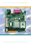
EmETX-i702
USER'S MANUAL
Copyright 2005
Copyright 2005 CONTEC CO., LTD. ALL RIGHTS RESERVED
INo part of this document may be copied or reproduced in any form by any means
without prior written consent of CONTEC CO., LTD.
CONTEC CO., LTD. makes no commitment to update or keep current the information
contained in this document. The information in this document is subject to change
without notice.
All relevant issues have been considered in the preparation of this document. Should
you notice an omission or any questionable item in this document, please feel free to
notify CONTEC CO., LTD.
Regardless of the foregoing statement, CONTEC assumes no responsibility for any
errors that may appear in this document nor for results obtained by the user as a
result of using this product.
Trademarks
Intel, Celeron and Pentium are registered trademarks of Intel Corporation.
MS, Microsoft, Windows and Windows NT are trademarks of Microsoft Corporation.
Other brand and product names are trademarks of their respective holder.
All Other product names or trademarks are properties of their respective owners.
EmETX-i702 User's Manual
2
Table of Contents
Specifications
Item
Specifications ............................................................................. 3
CPU (Option)
Specification
Intel(R) Pentium(R) M Processor 1.6G - 2.0GHz (FSB 400MHz), PGA
Intel(R) Celeron(R) M Processor 1.3G - 1.5GHz (FSB 400MHz), PGA
Cache
Built in CPU
Processor socket
Socket 479
Memory (Option)
One 200-pin SO-DIMM socket, PC2100 DDR SDRAM for up to 1GB
Chipset
Intel(R) 852GM+ICH4
BIOS
Award BIOS
Board Dimension ........................................................................ 5
VGA
Built in Intel(R) 815GME *1
Keyboard/Mouse connector
One Keyboard , One Mouse *1
Jumper/Connector Quick Reference ......................................... 5
Serial I/F
Board Layout Top View (Front) .................................................. 4
Board Layout Top View (Back) .................................................. 4
Two 16550 UART ports *1
Baud rate: 50 - 115,200bps (programmable)
Parallel I/F
One high-speed parallel port, support SPP/EPP/ECP mode *1
ETX Connector ............................................................................ 6
On board expansion bus
Four PCI bus slots possibility are mounting on a base board. *1
LAN Port
100BASE-TX/10BASE-T, Intel ICH4 integrated controller *1
System Resources ...................................................................... 7
IDE I/F
Two EIDE ports, up to four IDE devices, support Ultra DMA100 *1
SATA I/F
None
FDD I/F
None
Compact Flash Slot
None
SSD Socket
None
USB Port
4ch USB 2.0 complaint ports *1
IrDA
IrDA 1.1 complaint port *1
RAID
None
Audio
AC97 CODEC for speaker out, line in, CD Audio in, microphone in. *1
Watchdog Timer
Software programmable 255 levels (1 - 255sec). Reset occurrence at the time of time up.
General-purpose I/F
None
Hardware Monitor
Monitoring of the temperature of CPU, power supply voltage, and fan speed
AWARD BIOS Setup .................................................................... 9
Standard CMOS Setup ......................................................................................... 10
BIOS Features Setup ........................................................................................... 11
Chipset Features Setup ....................................................................................... 13
Integrated Peripherals ......................................................................................... 14
Super I/O Device .................................................................................................. 15
Power Management Setup .................................................................................. 16
PNP/PCI Configuration .......................................................................................... 17
PC Health Status .................................................................................................. 17
POST Codes .............................................................................. 18
RTC/CMOS *2
RTC/CMOS data backed up by Lithium battery
The backup time of the Lithium battery is over 4 years at 25°C.
The clock is accurate ±3 minutes/month at 25°C.
(When using PBE-1000)
Power Management
Power management setup via BIOS
Bus specification / Size (mm)
None / 114(W) x 95(D)
DC Power Requirements
+5VDC ±5%
Power supply specifications
Pentium M 1.6GHz
(Max.)
+5VDC 7A
Operating temperature /
Operating Humidity
0 - 50°C /10 - 90%RH (No condensation)
Storage temperature
-30 - 85°C
Floating dust particles
Not to be excessive
Corrosive gases
None
Weight
85g
Operating System Support
Windows XP Professional
Windows 2000 Professional
* 1 Wiring to the ETX connector and the connectors for the each devices, please mount them to the base board.
*2
EmETX-i702 User's Manual
When this product is equipped on the base board at first time, you have to clear CMOS. See PBE-1000 Quick Guide.
3
Board Layout Top View (Front)
Board Layout Top View (Back)
DDR SODIMM
ETX4
ETX2
ETX3
ETX1
ICH4
CPU
INTEL 855
GME
EmETX-i702 User's Manual
4
Board Dimension
Jumper/Connector Quick Reference
Connectors
Lable
Function
ETX1
PCI Bus, USB, Audio
ETX2
ISA Bus
ETX3
VGA,LCD,Video,COM1,COM2,LPT,IrDA,KB/MS
ETX4
IDE1,IDE2,Ethernet,Miscellaneous
UNIT: mm
EmETX-i702 User's Manual
5
ETX Connector
ETX1
1
3
5
7
9
11
13
15
17
19
21
23
25
27
29
31
33
35
37
39
41
43
45
47
49
51
53
55
57
59
61
63
65
67
69
71
73
75
77
79
81
83
85
87
89
91
93
95
97
99
GND
PCICLK3
GND
PCICLK1
REQ#3
GNT#2
REQ#2
REQ#1
GNT#0
VCC
SERIRQ
AD0
AD1
AD4
AD6
CBE#0
AD8
GND
AD10
AD11
AD12
AD13
AD14
AD15
CBE#1
VCC
PAR
PERR#
PME#
LOCK#
TRDY#
IRDY#
FRAME#
GND
AD16
AD17
AD19
AD20
AD22
AD23
AD24
VCC
AD25
AD28
AD27
AD30
PCIRST#
INTR#C
INTR#A
GND
GND
PCICLK4
GND
PCICLK2
GNT#3
VCC3
GNT#1
VCC3
N.C
VCC
REQ#0
VCC3
AD2
AD3
AD5
AD7
AD9
GND
AUXAL
MIC
AUXAR
ASVCC
SNDL
ASGND
SNDR
VCC
SERR#
N.C
USB2DEVSEL#
USB3STOP#
USB2+
GND
CBE#2
USB3+
AD18
USB0AD21
USB1CBE#3
VCC
AD26
USB0+
AD29
USB1+
AD31
INTR#D
INTR#B
GND
EmETX-i702 User's Manual
ETX2
2
4
6
8
10
12
14
16
18
20
22
24
26
28
30
32
34
36
38
40
42
44
46
48
50
52
54
56
58
60
62
64
66
68
70
72
74
76
78
80
82
84
86
88
90
92
94
96
98
100
1
3
5
7
9
11
13
15
17
19
21
23
25
27
29
31
33
35
37
39
41
43
45
47
49
51
53
55
57
59
61
63
65
67
69
71
73
75
77
79
81
83
85
87
89
91
93
95
97
99
GND
PCICLK3
SD14
GND
SD13
PCICLK1
SD12
REQ#3
SD11
GNT#2
SD10
REQ#2
SD9
REQ#1
SD8
GNT#0
MEMW#
VCC
MEMR#
SERIRQ
LA17
AD0
LA18
AD1
LA19
AD4
LA20
AD6
LA21
CBE#0
LA22
AD8
LA23
GND
AD10
SBHE#
AD11
SA0
AD12
SA1
AD13
SA2
AD14
SA3
AD15
SA4
CBE#1
SA5
VCC
SA6
PAR
PERR#
SA7
PME#
SA8
SA9
LOCK#
TRDY#
SA10
IRDY#
SA11
SA12
FRAME#
GND
AD16
SA13
AD17
SA14
SA15
AD19
AD20
SA16
AD22
SA18
SA19
AD23
IOCHRDY
AD24
VCC
AD25
SD0
SD2
AD26
AD27
SD3
AD30
DREQ2
SD5
PCIRST#
INTR#C
SD6
INTR#A
IOCHK#
GND
GND
SD15
MASTER#
DREQ7
DACK#7
DREQ6
DACK#6
DREQ5
DACK#5
DREQ0
DACK#0
IRQ14
IRQ15
IRQ12
IRQ11
IRQ10
IO16#
GND
M16#
OSC
BALE
TC
DACK#2
IRQ3
IRQ4
VCC
IRQ5
IRQ6
IRQ7
SYSCLK
REFCH#
DREQ1
DACK#1
GND
DREQ3
DACK#3
IOR#
IOW#
SA17
SMEMR#
AEN
VCC
SMEMW#
SD1
NOWS#
SD4
IRQ9
SD7
RSTDRV
GND
ETX4
ETX3
2
4
6
8
10
12
14
16
18
20
22
24
26
28
30
32
34
36
38
40
42
44
46
48
50
52
54
56
58
60
62
64
66
68
70
72
74
76
78
80
82
84
86
88
90
92
94
96
98
100
1
3
5
7
9
11
13
15
17
19
21
23
25
27
29
31
33
35
37
39
41
43
45
47
49
51
53
55
57
59
61
63
65
67
69
71
73
75
77
79
81
83
85
87
89
91
93
95
97
99
GND
R
HSY
VSY
N.C/DE
TX2CLK#
TX2CLK+
GND
TX2D1+
TX2D1#
GND
TX1D3#
TX1D3+
GND
TX1D2#
TX1D2+
GND
TX1D0+
TX1D0#
VCC
N.C.
N.C
BIASON
N.C
N.C
N.C
VCC
STB#
I.C
IRRX
IRTX
RXD2
GND
RTS#2
DTR#2
DCD#2
DSR#2
CTS#2
TXD#2
RI#2
VCC
RXD1
RTS#1
DTR#1
DCD#1
DSR#1
CTS#1
TXD#1
RI#1
GND
GND
B
G
DDCK
DDDA
TX2D3#
TX2D3+
GND
TX2D2+
TX2D2#
GND
TX2D0+
TX2D0#
GND
TX1CLK+
TX1CLK#
GND
TX1D1+
TX1D1#
VCC
N.C
BLON
DIGON
N.C
N.C
N.C
GND
AFD#
PD7
ERR#
PD6
INIT#
GND
PD5
SLIN#
PD4
PD3
PD2
PD1
PD0
VCC
ACK#
BUSY#
PE
SLCT#
MSCLK
MSDAT
KBCLK
KBDAT
GND
2
4
6
8
10
12
14
16
18
20
22
24
26
28
30
32
34
36
38
40
42
44
46
48
50
52
54
56
58
60
62
64
66
68
70
72
74
76
78
80
82
84
86
88
90
92
94
96
98
100
1
3
5
7
9
11
13
15
17
19
21
23
25
27
29
31
33
35
37
39
41
43
45
47
49
51
53
55
57
59
61
63
65
67
69
71
73
75
77
79
81
83
85
87
89
91
93
95
97
99
GND
SV_SB
PS_ON
PWRBTN#
N.C
WDTOUT
ROMKBCS#
N.C
VCC
OVCR#
EXTSMI#
SMBCLK
SIDE_CS3#
SIDE_CS1#
SIDE_A2
SIDE_A0
GND
PD33/66 SEL
SIDE_A1
SIDE_INTRQ
SD33/66 SEL
SIDE_ACK#
SIDE_RDY
SIDE_IOR#
VCC
SIDE_IOW#
SIDE_DRQ
SIDE_D15
SIDE_D0
SIDE_D14
SIDE_D1
SIDE_D13
GND
SIDE_D2
SIDE_D12
SIDE_D3
SIDE_D11
SIDE_D4
SIDE_D10
SIDE_D5
VCC
SIDE_D9
SIDE_D6
SIDE_D8
RING IN
RXDRXD+
TXDTXD+
GND
GND
PWGIN
SPEAKER
BATT
LILED
ACTLED
SPEEDLED
12CLK
VCC
GPCS#
12DAT
SMBDAT
CPUFAN
DASP#
PIDE_CS3#
PIDE_CS1#
GND
PIDE_A2
PIDE_A0
PIDE_A1
N.C
PIDE_INTRQ
PIDE_ACK#
PIDE_RDY
VCC
PIDE_IOR#
PIDE_IOW#
PIDE_DRQ
PIDE_D15
PIDE_D0
PIDE_D14
PIDE_D1
GND
PIDE_D13
PIDE_D2
PIDE_D12
PIDE_D3
PIDE_D11
PIDE_D4
PIDE_D10
VCC
PIDE_D5
PIDE_D9
PIDE_D6
WOL
PIDE_D8
SIDE_D7
PIDE_D7
HDRST#
GND
2
4
6
8
10
12
14
16
18
20
22
24
26
28
30
32
34
36
38
40
42
44
46
48
50
52
54
56
58
60
62
64
66
68
70
72
74
76
78
80
82
84
86
88
90
92
94
96
98
100
6
System Resources
Interrupt Request (IRQ)
IRQ Address
Description
IRQ 00
System timer
IRQ 01
Standard 101/102-Key or Microsoft Natural Keyboard
IRQ 02
Programmable interrupt controller
IRQ 03
Communications Port (COM2)
IRQ 04
Communications Port (COM1)
IRQ 05
PCI Multimedia Audio Device
IRQ 05
PCI System Management Bus
IRQ 05
IRQ Holder for PCI Steering
IRQ 07
Printer Port (LPT1)
IRQ 08
System CMOS/real time clock
IRQ 09
PCI Universal Serial Bus
IRQ 09
IRQ Holder for PCI Steering
IRQ 0A
Standard Universal PCI to USB Host Controller
IRQ 0A
Standard Universal PCI to USB Host Controller
IRQ 0A
IRQ Holder for PCI Steering
IRQ 0A
Standard PCI Graphics Adapter (VGA)
IRQ 0B
Intel(R) PRO/100 VE Network Connection
IRQ 0B
Standard Universal PCI to USB Host Controller
IRQ 0B
IRQ Holder for PCI Steering
IRQ 0C
PS/2 Compatible Mouse Port
IRQ 0D
Numeric data processor
IRQ 0E
Primary IDE controller (single fifo)
IRQ 0E
Standard Dual PCI IDE Controller
IRQ 0F
Secondary IDE controller (single fifo)
IRQ 0F
Standard Dual PCI IDE Controller
Direct Memory Access (DMA)
DMA
Description
4
Direct memory access controller
EmETX-i702 User's Manual
Ports Input/Output (IO)
I/O Address
Description
Memory 00000000-0009FFFF
System board extension for PnP BIOS
Memory 00000000-FFFFFFFF
PCI standard PCI-to-PCI bridge
Memory 00000000-FFFFFFFF
PCI standard PCI-to-PCI bridge
Memory 00000000-FFFFFFFF
PCI standard PCI-to-PCI bridge
Memory 000A0000-000AFFFF
Standard PCI Graphics Adapter (VGA)
Memory 000B0000-000BFFFF
Standard PCI Graphics Adapter (VGA)
Memory 000C0000-000CC7FF
Standard PCI Graphics Adapter (VGA)
Memory 000D8000-000D97FF
Intel(R) PRO/100 VE Network Connection
Memory 000D9800-000DBFFF
Motherboard resources
Memory 000F0000-000F3FFF
Motherboard resources
Memory 000F4000-000F7FFF
Motherboard resources
Memory 000F8000-000FFFFF
Motherboard resources
Memory 00100000-00FFFFFF
System board extension for PnP BIOS
Memory D0000000-D7FFFFFF
Standard PCI Graphics Adapter (VGA)
Memory D8000000-DFFFFFFF
Standard PCI Graphics Adapter
Memory E0000000-E3FFFFFF
PCI standard host CPU bridge
Memory E4000000-E4000FFF
Intel(R) PRO/100 VE Network Connection
Memory E4000000-E40FFFFF
PCI standard PCI-to-PCI bridge
Memory E4100000-E417FFFF
Standard PCI Graphics Adapter
Memory E4180000-E41FFFFF
Standard PCI Graphics Adapter (VGA)
Memory E4200000-E42003FF
PCI Universal Serial Bus
Memory E4201000-E42011FF
PCI Multimedia Audio Device
Memory E4202000-E42020FF
PCI Multimedia Audio Device
Memory FEC00000-FEC0FFFF
System board extension for PnP BIOS
Memory FEE00000-FEE0FFFF
System board extension for PnP BIOS
Memory FFB00000-FFB7FFFF
System board extension for PnP BIOS
Memory FFB80000-FFBFFFFF
Unknown Device
Memory FFF00000-FFFFFFFF
System board extension for PnP BIOS
Port 0000-FFFF
PCI standard PCI-to-PCI bridge
7
Port 0020-0021
Programmable interrupt controller
Port A400-A41F
Standard Universal PCI to USB Host Controller
Port 0040-0043
System timer
Port A800-A81F
Standard Universal PCI to USB Host Controller
Port 0060-0060
Standard 101/102-Key or Microsoft Natural Keyboard
Port AC00-AC07
Standard PCI Graphics Adapter (VGA)
Port 0061-0061
System speaker
Port B400-B4FF
PCI Multimedia Audio Device
Port 0070-0071
System CMOS/real time clock
Port B800-B83F
PCI Multimedia Audio Device
Direct memory access controller
Port F000-F007
Primary IDE controller (single fifo)
Port 0087-0087
Direct memory access controller
Port F000-F00F
Standard Dual PCI IDE Controller
Port 0089-008B
Direct memory access controller
Port F008-F00F
Secondary IDE controller (single fifo)
Port 008F-0091
Direct memory access controller
Port 00A0-00A1
Programmable interrupt controller
Port 00C0-00DF
Direct memory access controller
Port 00F0-00FF
Numeric data processor
Port 0170-0177
Secondary IDE controller (single fifo)
Port 0170-0177
Standard Dual PCI IDE Controller
Port 01F0-01F7
Primary IDE controller (single fifo)
Port 01F0-01F7
Standard Dual PCI IDE Controller
Port 02F8-02FF
Communications Port (COM2)
Port 0376-0376
Secondary IDE controller (single fifo)
Port 0376-0376
Standard Dual PCI IDE Controller
Port 0378-037F
Printer Port (LPT1)
Port 03B0-03BB
Standard PCI Graphics Adapter (VGA)
Port 03C0-03DF
Standard PCI Graphics Adapter (VGA)
Port 03F6-03F6
Primary IDE controller (single fifo)
Port 03F6-03F6
Standard Dual PCI IDE Controller
Port 03F8-03FF
Communications Port (COM1)
Port 0400-04BF
PCI bus
Port 04D0-04D1
PCI bus
Port 0500-051F
PCI System Management Bus
Port 0778-077B
Printer Port (LPT1)
Port 0CF8-0CFF
PCI bus
Port 9000-903F
Intel(R) PRO/100 VE Network Connection
Port 9000-9FFF
PCI standard PCI-to-PCI bridge
Port A000-A01F
Standard Universal PCI to USB Host Controller
Port 0081-0083
EmETX-i702 User's Manual
8
AWARD BIOS Setup
The EmETX-i702 uses the Award PCI/ISA BIOS for the system configuration.
The Award BIOS setup program is designed to provide the maximum flexibility in
configuring the system by offering various options which could be selected for enduser requirements. This chapter is written to assist you in the proper usage of these
features.
To access AWARD PCI/ISA BIOS Setup program, press <Del> key. The Main Menu will
be displayed at this time.
Setup Items
The main menu includes the following main setup categories. Recall that some
systems may not include all entries.
Standard CMOS Features
Use this menu for basic system configuration.
Advanced BIOS Features
Use this menu to set the Advanced Features available on your system.
Advanced Chipset Features
Use this menu to change the values in the chipset registers and optimize your system's
performance.
Integrated Peripherals
Use this menu to specify your settings for integrated peripherals.
Power Management Setup
Use this menu to specify your settings for power management.
PnP / PCI Configuration
This entry appears if your system supports PnP / PCI.
PC Health Status
This entry helps you to monitor the status of PC.
Load Optimized Defaults
Use this menu to load the BIOS default values that are factory settings for optimal
performance system operations. W hile Award has designed the custom BIOS to
maximize performance, the factory has the right to change these defaults to meet their
needs.
Set Password
Use this menu to set User and Supervisor Passwords.
Once you enter the AwardBIOS™ CMOS Setup Utility, the Main Menu will appear on the
screen. The Main Menu allows you to select from several setup functions and two
exit choices. Use the arrow keys to select among the items and press <Enter> to
accept and enter the sub-menu.
EmETX-i702 User's Manual
Save & Exit Setup
Save CMOS value changes to CMOS and exit setup.
Exit Without Save
Abandon all CMOS value changes and exit setup.
9
Standard CMOS Setup
Video Select the type of primary video subsystem in your computer. The BIOS usually
detects the correct video type automatically. The BIOS supports a secondary video
subsystem, but you do not select it in Setup.
Halt On
During the power-on self-test (POST), the computer stops if the BIOS
detects a hardware error. You can tell the BIOS to ignore certain errors during POST
and continue the boot-up process. These are the selections:
No errors
POST does not stop for any errors.
All errors
If the BIOS detects any non-fatal error, POST stops and prompts
you to take corrective action.
All, But Keyboard
POST does not stop for a keyboard error, but stops for all other
errors.
All, But Diskette
POST does not stop for diskette drive errors, but stops for all
other errors.
All, But Disk/Key
POST does not stop for a keyboard or disk error, but stops for
all other errors.
Date
The BIOS determines the day of the week from the other date information; this field is
for information only.
Time
The time format is based on the 24-hour military-time clock. For example, 1 p.m. is
13:00:00. Press the « or ( key to move to the desired field . Press the PgUp or PgDn
key to increment the setting, or type the desired value into the field.
IDE Primary Master/Slave
IDE Secondary Master/Slave
Options are in sub menu (see page 30)
Drive A, B
Select the correct specifications for the diskette drive(s) installed in the computer.
None : No diskette drive installed
360K ; 5.25 in 5-1/4 inch PC-type standard drive
1.2M ; 5.25 in 5-1/4 inch AT-type high-density drive
720K ; 3.5 in 3-1/2 inch double-sided drive
1.44M ;
3.5 in 3-1/2 inch double-sided drive
2.88M ;
3.5 in 3-1/2 inch double-sided drive
EmETX-i702 User's Manual
10
BIOS Features Setup
CPU L1 & L2 Cache
This item allows you to enable/disable CPU L1 & L2 Cache.
The choice: Enabled, Disabled.
CPU L3 Cache
This item allows you to enable/disable CPU L3 Cache.
The choice: Enabled, Disabled.
Quick Power On Self Test
This category speeds up Power On Self Test (POST) after you power up the computer. If it is set to Enable, BIOS will shorten or skip some check items during POST.
Enabled : Enable quick POST. Disabled : Normal POST
First/Second/Third Boot Device
The BIOS attempts to load the operating system from the devices in the sequence
selected in these items. The choices are : Floppy, LS/ZIP, HDD, SCSI, CDROM, Disabled.
Swap Floppy Drive
If the system has two floppy drives, you can swap the logical drive name assignments. The choice: Enabled/Disabled.
Boot Up Floppy Seek
Seeks disk drives during boot up. Disabling speeds boot up.
The choice: Enabled/Disabled.
Virus Warning
Allows you to choose the VIRUS Warning feature for IDE Hard Disk boot sector
protection. If this function is enabled and someone attempt to write data into this
area, BIOS will show a warning message on screen and beep.
Enabled Activates automatically when the system boots up causing a warning
message to appear when anything attempts to access the boot sector or
hard disk partition table.
Disabled No warning message will appear when anything attempts to access the boot
sector or hard disk partition table.
EmETX-i702 User's Manual
Boot Up NumLock Status
Select power on state for NumLock. The choice: Enabled/Disabled.
Gate A20 Option
Select if chipset or keyboard controller should control GateA20.
Normal A pin in the keyboard controller controls GateA20
Fast
Lets chipset control GateA20
Typematic Rate Setting
Key strokes repeat at a rate determined by the keyboard controller. When enabled, the
typematic rate and typematic delay can be selected.
The choice: Enabled/Disabled.
11
Security Option
Select whether the password is required every time the system boots or only when
you enter setup.
'Memory'. This will tell you what segments (if any) are being shadowed For DOS you
can use MSD.EXE to see what segments are claimed.
CC000-CFFFF - D0000-D3FFF - D4000-D7FFF - D8000-DBFFF and
DC000-DFFFF - Same as above.
System The system will not boot and access to Setup will be denied if the correct
password is not entered at the prompt.
Setup
The system will boot, but access to Setup will be denied if the correct
password is not entered at the prompt.
Note
To disable security, select PASSWORD SETTING at Main Menu and then you
will be asked to enter password. Do not type anything and just press
<Enter>, it will disable security. Once the security is disabled, the system will
boot and you can enter Setup freely.
APIC Mode
Select
OS Select For DRAM > 64MB
Select the operating system that is running with greater than 64MB of RAM on the
system.The choice: Non-OS2, OS2.
Video BIOS Shadow
Enabled this copies the video BIOS from ROM to RAM. effectively enhancing performance, and reducing the amount of upper memory available by 32KB (the
C0000~C7FFF area of memory between 640 KB and 1 MB is used).
C8000-CBFFF Shadow
Enabling any of the C8000~CBFFF segments allows components to move their
firmware into these upper memory segments. However your computer can lock-up
doing so, because some devices don't like being shadowed at those particular 16 KB
segments of upper memory.
Small Logo(EPA) Show
[Enabled]: If you want to show your logo, please enable it.
[Disabled]: When this item disabled, logo(EPA) will not show on screen.
EEPROM Write Protect
All the configuration data is stored in a type of nonvolatile memor chip called an
EEPROM. When it's enabled, it disables all writes to the configuration EEPROM. This
locks your current configuration against accidenatal or unauthorized changes.
Note - In W indows 95, double click 'Computer' within Device Manager and select
EmETX-i702 User's Manual
12
Chipset Features Setup
DRAM Data Integrity Mode
This BIOS feature controls the ECC feature of the memory controller. The option is ECC
or Non-ECC.
MGM Core Frequency
The option includes 400/266/133/200 MHz.
System BIOS Cacheable
Selecting Enabled allows caching of the system BIOS ROM at F0000h-FFFFFh, resulting
in better system performance. However, if any program writes to this memory area, a
system error may result.
Video BIOS Cacheable
Select Enabled allows caching of the video BIOS, resulting in better system performance. However, if any program writes to this memory area, a system error may
result.
DRAM Timing Selectable
The option is "Manual" or "by SPD.
CAS Latency Time
When synchronous DRAM is installed, the number of clock cycles of CAS latency
depends on the DRAM timing.
Memory Hole At 15M-16M
You can reserve this area of system memory for ISA adapter ROM. When this area is
reserved, it cannot be cached. The user information of peripherals that need to use
this area of system memory usually discusses their memory requirement.
Delayed Transaction
The chipset has an embedded 32-bit posted write buffer to support delay transactions
cycles. Select Enabled to support compliance with PCI specification version 2.1
Delay Prior to Thermal
Active to Precharge Delay
Delay that results when two different rows in a memory chip are addressed one after
another.
DRAM RAS-to-CAS Delay
This field let's you insert a timing delay between the CAS and RAS strobe signals,
used when DRAM is written to, read from, or refreshed. Fast gives faster performance; and Slow gives more stable performance. This field applies only when
synchronous DRAM is installed in the system.
DRAM RAS Precharge
If an insufficient number of cycles is allowed for the RAS to accumulate its charge
before DRAM refresh, the refresh may be incomplete and the DRAM may fail to retain
data. Fast gives faster performance; and Slow givesmore stable performance. This
field applies only when synchronous DRAM is installed in the system.
EmETX-i702 User's Manual
This BIOS feature is only valid for systems that are powered by 0.13£g Intel Pentium 4
processors with 512KB L2 cache. These processors come with a Thermal Monitor
which actually consists of a on-die thermal sensor and a Thermal Control Circuit (TCC).
The options includes 4 Minutes, 8 Minutes, 16 Minutes, 32.
AGP Aperture Size
This fielf determines the effective size of the Graphic Aperture used for a particular
GMCH configuration. It can be updated by the GMCH-specific BIOS configuration
sequence before the PCI standard bus enumeration sequence takes place. If it is not
updated then a default value will select an aperture of maximum size.
On-Chip VGA
If your system contains a VGA controller and you want to activate it, select Enabled.
The next option will become available.
13
On-Chip Frame Buffer Size
Integrated Peripherals
The On-Chip Frame Buffer Size can be set to 1MB or 8MB. This memory is shared with
system memory.
Boot Display
This option let you select the display devices.
Panel Number
This option let you select the type of panel. Available options are:
640 x 480
18bit
800 x 600
18bit
1024 x 768
18bit
1280 x 1024
18bit
1400 x 1050
18bit 2H (Reduced Blanking LVDS)
1400 x 1050
18bit 2H (Non-reduced Blanking LVDS)
1600 x 1200
18bit 2H
1024 x 768
24bit
1280 x 1024
24bit 2H
1400 x 1050
24bit 2H
Onboard Device
This field let you set onboard devices.
1600 x 1200
24bit 2H
Super I/O Device
OnChip IDE Device
The integrated peripheral controller contains an IDE interface with support for two IDE
channels. Select Enabled to activate each channel separately.
>Onboard LAN Boot ROM
The default setting is "Disabled" that to shorten the booting time.
EmETX-i702 User's Manual
14
Super I/O Device
IR Transmission Delay
This option is to set whether the IR Transmission Delay is enabled. The available
setting values are Disabled and Enabled.
IR2 Duplex Mode
This item allows you to select the IR half/full duplex function.
Use IR Pins
This item allows you to select IR transmission routes, IR-Rx2Tx2, RxD2 and TxD2.
Onboard Parallel Port
Select the interrup of Parallel Port.
Onboard Parallel Mode
Select an operating mode for the parallel port. Mode options are 3BC/IRQ7, 378/IRQ7,
278/IRQ5, and Disable.
External FDC Controller
EPP Mode Select
You can use this feature to choose which version of EPP to use. For better performance, use EPP 1.9. But if you are facing connection issues, try setting it to EPP 1.7.
Most of the time, EPP 1.9 will work perfectly well.
Select "Enabled" to activate the on-board FDD
Select "Disabled" to activate an add-on FDD
ECP Mode Use DMA
Select a DMA channel if parallel Mode for using ECP mode: 3 or 1.
Onboard Serial Port 1 & 2
Select an address and corresponding interrupt for the first/second serial port. The
default value for the first serial port is "3F8/IRQ4" and the second serial port is "2F8/
IRQ3".
Secondary I/O Controller
This item let you disable or enable Secondary I/O Controller.
UART Mode Select
This item allows you to select UART mode. The choices: IrDA, ASKIR, Normal.
RxD, TxD Active
This BIOS feature allows you to set the infra-red reception (RxD) and transmission
(TxD) polarity. Common Options : Hi, Hi or Lo, Lo or Hi, Lo or Lo, Hi
EmETX-i702 User's Manual
15
Power Management Setup
V/H SYNC+Blank
cause the system to turn off the vertical and horizontal synchronization signals and writes blanks to the screen.
Blank Screen
This option only writes blanks to the screen.
DPMS
Initial display power management signaling.HDD Power Down is
always set independently
Video Off In Suspend
Controls what causes the display to be switched off
Suspend -> Off
Always On
All Mode -> Off
Suspend Type
S1 (POS)
Power On suspend
All devices are powered up except for the clock synthesizer. The Host and PCI clocks
are inactive and PIIX4 provides control signals and 32-kHz Suspend Clock (SUSCLK) to
allow for DRAM refresh and to turn off the clock synthesizer. The only power
consumed in the system is due to DRAM Refresh and leakage current of the powered
devices. When the system resumes from POS, PIIX4 can optionally resume without
resetting the system, can reset the processor only, or can reset the entire system.
When no reset is performed, PIIX4 only needs to wait for the clock synthesizer and
processor PLLs to lock before the system is resumed. This takes typically 20 ms.
Power Supply Type
Select the power supply type.
Power Management
There are 4 selections for Power Management, 3 of which have fixed mode :
S3 (STR) Suspend To RAM
Power is removed from most of the system components during STR, except the DRAM.
Power is supplied to Suspend Refresh logic in the Host Controller, and RTC and
Suspend Well logic in PIIX4. PIIX4 provides control signals and 32-kHz Suspend Clock
(SUSCLK) to allow for DRAM refresh and to turn off the clock synthesizer and other
power planes.
Disabled (default)
No power management. Disables all four modes.
Min. Power Saving
Minimum power management. Doze Mode = 1 hr.,
Standby Mode = 1 hr., Suspend Mode = 1 hr.,
Modem Use IRQ
Name the interrupt request (IRQ) assigned to the modem (if any) on your system.
Activity of the selected IRQ always awakens the system.
Max. Power Saving
Maximum power management -- ONLY AVAILABLE FOR SL
CPU's.. Doze Mode = 1 min., Standby Mode = 1 min., Suspend
Mode = 1 min.
Suspend Mode
When the suspend mode has been enabled after the selected period of system
inactivity, all devices except CPU will be shut down.
User Defined
Allows you to set each mode individually. When not disabled,
each of the ranges are from 1 min. to 1 hr.
CPU THRM-Throtting
Video Off Method
This determines the manner in which the monitor is blanked.
EmETX-i702 User's Manual
This BIOS feature determines the clock speed of the processor when it is in the
Suspend To RAM (STR) power saving mode. It has no effect when the processor is in
normal active mode. Available options for this BIOS feature are set values of the
processor's power consumption. They range from a low of 12.5% to a high of 87.5%.
16
PNP/PCI Configuration
PC Health Status
This section describes configuring the PCI bus system. PCI, or Personal Computer
Interconnect, is a system which allows I/O devices to operate at speeds nearing the
speed the CPU itself uses when communicating with its own special components.
This section describes CPU tempeare for the system.
Reset Configuration Data
Normally, you leave this field Disabled. Select Enabled to reset ESCD (Extended System
Configuration Date) when you exit Setup if you have installed a new add-on and the
system reconfiguration has caused such a serious conflict that the operating system
cannot boot.
Shutdown Temperature
This item allows you to set up the CPU shutdowm Temperature. This item only
effective under Windows 98 ACPI mode.
Resource Controlled By
The Award Play and Play BIOS can automatically configure all the boot and Plug-andPlay compatible devices. If you select Auto, all the interrupt request (IRQ) and DMA
assignment fields disappear, as the BIOS automatically assigns them.
PCI/VGA Palette Snoop
Normally this option is always Disabled! Nonstandard VGA display adapters such as
overlay cards or MPEG video cards may not show colors properly. Setting Enabled
should correct this problem. If this field set Enabled, any I/O access on the ISA bus to
the VGA card's palette registers will be reflected on the PCI bus. This will allow
overlay cards to adapt to the changing palette colors.
PCI IRQ Actived by
[Level]
EmETX-i702 User's Manual
17
POST Codes
0Ah
The following codes are not displayed on the screen. They can only be viewed on the
LED display of a so called POST card. The codes are listened in the same order as the
according functions are executed at PC startup. If you have access to a POST Card
reader, you can watch the system perform each test by the value that's displayed. If
the system hangs (if there's a problem) the last value displayed will give you a good
idea where and what went wrong, or what's bad on the system board.
1. Disable PS/2 mouse interface (optional).
2. Auto detect ports for keyboard & mouse followed by a
port & interface swap (optional).
3. Reset keyboard for Winbond 977 series Super I/O chips.
0Bh
Reserved
0Ch
Reserved
0Dh
Reserved
CODE
DESCRIPTION OF CHECK
0Eh
CFh
Test CMOS R/W functionality.
Test F000h segment shadow to see whether it is R/W-able or not. If
test fails, keep beeping the speaker.
C0h
Early chipset initialization:
-Disable shadow RAM
-Disable L2 cache (socket 7 or below)
-Program basic chipset registers
C1h
Detect memory
-Auto-detection of DRAM size, type and ECC.
-Auto-detection of L2 cache (socket 7 or below)
0Fh
Reserved
10h
Auto detect flash type to load appropriate flash R/W codes into the run
time area in F000 for ESCD & DMI support.
11h
Reserved
12h
Use walking 1's algorithm to check out interface in CMOS circuitry.
Also set real-time clock power status, and then check for override.
C3h
Expand compressed BIOS code to DRAM
13h
Reserved
C5h
Call chipset hook to copy BIOS back to E000 & F000
shadow RAM.
14h
Program chipset default values into chipset. Chipset default values are
MODBINable by OEM customers.
0h1
Expand the Xgroup codes locating in physical address 1000:0
15h
Reserved
02h
Reserved
16h
03h
Initial Superio_Early_Init switch.
Initial onboard clock generator if Early_Init_Onboard_Generator is
defined. See also POST 26h.
04h
Reserved
17h
Reserved
05h
1. Blank out screen
2. Clear CMOS error flag
18h
Detect CPU information including brand, SMI type (Cyrix or Intel) and
CPU level (586 or 686).
06h
Reserved
19h
Reserved
07h
1. Clear 8042 interface
2. Initialize 8042 self-test
1Ah
Reserved
1Bh
1. Test special keyboard controller for Winbond 977
series Super I/O chips.
2. Enable keyboard interface.
Initial interrupts vector table. If no special specified, all H/W interrupts
are directed to SPURIOUS_INT_HDLR & S/W interrupts to
SPURIOUS_soft_HDLR.
1Ch
Reserved
Reserved
1Dh
Initial EARLY_PM_INIT switch.
08h
09h
EmETX-i702 User's Manual
18
CPU type, CPU speed, full screen logo.
1Eh
Reserved
1Fh
Load keyboard matrix (notebook platform)
2Eh
Reserved
20h
Reserved
2Fh
Reserved
21h
HPM initialization (notebook platform)
30h
Reserved
22h
Reserved
31h
Reserved
23h
1. Check validity of RTC value: e.g. a value of 5Ah is an invalid value
for RTC minute.
2. Load CMOS settings into BIOS stack. If CMOS checksum fails, use
default value instead.
32h
Reserved
33h
Reset keyboard if Early_Reset_KB is defined e.g. Winbond 977 series
Super I/O chips. See also POST 63h.
34h
Reserved
35h
Test DMA Channel 0
36h
Reserved
37h
Test DMA Channel 1.
38h
Reserved
39h
Test DMA page registers.
3Ah
Reserved
3Bh
Reserved
24h
Prepare BIOS resource map for PCI & PnP use. If ESCD is valid, take
into consideration of the ESCD's legacy information.
25h
Early PCI Initialization:
-Enumerate PCI bus number.
-Assign memory & I/O resource
-Search for a valid VGA device & VGA BIOS,
and put it into C000:0
26h
1. If Early_Init_Onboard_Generator is not defined Onboard
clock generator initialization. Disable respective clock
resource to empty PCI & DIMM slots.
2. Init onboard PWM
3. Init onboard H/W monitor devices
3Ch
Test 8254
27h
Initialize INT 09 buffer
3Dh
Reserved
28h
Reserved
3Eh
Test 8259 interrupt mask bits for channel 1.
29h
1. Program CPU internal MTRR (P6 & PII)
for 0-640K memory address.
2. Initialize the APIC for Pentium class CPU.
3. Program early chipset according to CMOS setup.
Example: onboard IDE controller.
4. Measure CPU speed.
3Fh
Reserved
40h
Test 8259 interrupt mask bits for channel 2.
41h
Reserved
42h
Reserved
2Ah
Reserved
43h
Test 8259 functionality.
2Bh
Invoke Video BIOS
44h
Reserved
2Ch
Reserved
45h
Reserved
2Dh
1. Initialize double-byte language font (Optional)
2. Put information on screen display, including Award title,
46h
Reserved
47h
Initialize EISA slot
EmETX-i702 User's Manual
19
48h
Reserved
5Ch
Reserved
49h
1. Calculate total memory by testing the last double
word of each 64K page.
2. Program write allocation for AMD K5 CPU.
5Dh
1. Initialize Init_Onboard_Super_IO
2. Initialize Init_Onbaord_AUDIO.
5Eh
Reserved
4Ah
Reserved
5Fh
Reserved
4Bh
Reserved
60h
4Ch
Reserved
Okay to enter Setup utility; i.e. not until this POST stage can users enter
the CMOS setup utility.
4Dh
Reserved
61h
Reserved
4Eh
1. Program MTRR of M1 CPU
2. Initialize L2 cache for P6 class CPU & program
CPU with proper cacheable range.
3. Initialize the APIC for P6 class CPU.
4. On MP platform, adjust the cacheable range to smaller
one in case the cacheable ranges between each CPU
are not identical.
62h
Reserved
63h
Reset keyboard if Early_Reset_KB is not defined.
64h
Reserved
65h
Initialize PS/2 Mouse
66h
Reserved
4Fh
Reserved
67h
50h
Initialize USB Keyboard & Mouse.
Prepare memory size information for function call:
INT 15h ax=E820h
51h
Reserved
68h
Reserved
52h
Test all memory (clear all extended memory to 0)
69h
Turn on L2 cache
53h
Clear password according to H/W jumper (Optional)
6Ah
Reserved
54h
Reserved
6Bh
Program chipset registers according to items described in Setup & Autoconfiguration table.
55h
Display number of processors (multi-processor platform)
6Ch
Reserved
56h
Reserved
6Dh
57h
1. Display PnP logo
2. Early ISA PnP initialization
-Assign CSN to every ISA PnP device.
1. Assign resources to all ISA PnP devices.
2. Auto assign ports to onboard COM ports if the
corresponding item in Setup is set to "AUTO".
6Eh
Reserved
58h
Reserved
6Fh
59h
Initialize the combined Trend Anti-Virus code.
1. Initialize floppy controller
2. Set up floppy related fields in 40:hardware.
5Ah
Reserved
70h
Reserved
5Bh
(Optional Feature) Show message for entering AWDFLASH.EXE from
FDD (optional)
71h
Reserved
72h
Reserved
EmETX-i702 User's Manual
20
73h
(Reserved
86h
Reserved
74h
Reserved
87h
NET PC: Build SYSID Structure.
75h
Detect & install all IDE devices: HDD, LS120, ZIP, CDROM…..
88h
Reserved
76h
(Optional Feature)
Enter AWDFLASH.EXE if:
-AWDFLASH.EXE is found in floppy drive.
-ALT+F2 is pressed.
89h
1. Assign IRQs to PCI devices
2. Set up ACPI table at top of the memory.
8Ah
Reserved
77h
Detect serial ports & parallel ports.
8Bh
1. Invoke all ISA adapter ROMs
2. Invoke all PCI ROMs (except VGA)
78h
Reserved
8Ch
Reserved
79h
Reserved
8Dh
7Ah
Detect & install co-processor
1. Enable/Disable Parity Check according to CMOS setup
2. APM Initialization
7Bh
Reserved
8Eh
Reserved
7Ch
Init HDD write protect.
8Fh
Clear noise of IRQs
7Dh
Reserved
90h
Reserved
7Eh
Reserved
91h
Reserved
7Fh
Switch back to text mode if full screen logo is supported.
- If errors occur, report errors & wait for keys
- If no errors occur or F1 key is pressed to continue :
wClear EPA or customization logo.
92h
Reserved
93h
Read HDD boot sector information for Trend Anti-Virus code
94h
1.
2.
3.
4.
5.
6.
7.
8.
95h
Update keyboard LED & typematic rate
96h
1.
2.
3.
4.
5.
FFh
Boot attempt (INT 19h)
80h
Reserved
81h
Reserved
E8POST.ASM starts
82h
1. Call chipset power management hook.
2. Recover the text fond used by EPA logo
(not for full screen logo)
3. If password is set, ask for password.
83h
Save all data in stack back to CMOS
84h
Initialize ISA PnP boot devices
85h
1. USB final Initialization
2. Switch screen back to text mode
EmETX-i702 User's Manual
Enable L2 cache
Program Daylight Saving
Program boot up speed
Chipset final initialization.
Power management final initialization
Clear screen & display summary table
Program K6 write allocation
Program P6 class write combining
Build MP table
Build & update ESCD
Set CMOS century to 20h or 19h
Load CMOS time into DOS timer tick
Build MSIRQ routing table.
21