1
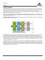
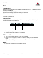
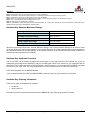
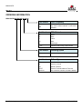
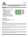
BRM1553FE May 2011 MIL-STD-1553B IP CORE FOR FPGA FEATURES Mil-Std-1553 Intellectual Property for FPGAs and ASICs Suitable for any Mil-Std-1553 BC, RT, MT implementation Very simple interface, does not require CPU for management, no SW required Very small FPGA area utilization Supports any even-clock frequency Modular architecture allows flexible implementations Provided with full verification environment Passed full RT validation testing by 3rd party Eliminates risk related to part obsolescence Based on vendor and technology-independent VHDL code APPLICATIONS Mil-Std-1553 Remote Terminal Mil-Std-1553 Remote Terminal with Message Monitor Mil-Std-1553 Bus Controller DESCRIPTION The BRM1553FE IP Core is suitable for small and simple Mil-Std-1553 implementations where no CPU is present or required, where relatively short messages are sent over the bus or where user‟s hardware manages the sent and received data. In such applications, a Remote Terminal (RT) is controlled directly by messages sent by the Mil-Std1553B bus controller (BC). Typically, such RTs will not need to incorporate a central processing unit (CPU) or its software to correlate between the terminal and the Mil-Std-1553 bus. The core incorporates a backend logic that arranges the messages in a predefined memory structure according to the sub-address of each message. Every message received from the bus will initiate „Write‟ cycles to the back-end and every message that should be transmitted to the bus will initiate „Read‟ cycles, where the data address is defined by the message sub-address from the 1553 bus. BRM1553FE can be used on any FPGA using any even-clock frequency (in MHz) and memory size. This ensures quick and reliable integration with the application design. The parametrically-settable clock frequency can be set from 12 Mhz and higher reducing the number of clock domains in the design. Designed from ground up for use in aerospace, avionics and military Mil-Std-1553 applications, Sital's Mil-Std-1553 IP products offer uniquely compact, robust and reliable BC, RT, MT solutions for any PLD/FPGA and ASIC device. They have been developed with the company's unflagging commitment to quality and excellence and with strict adherence to the stringent requirements of military and aerospace specifications. Sital Technology Page 1 of 9 Rev. 050111 BRM1553FE May 2011 BLOCK DIAGRAM The BRM1553FE core incorporates two decoders that translate serial bus messages from the Mil-Std-1553 Manchester coding and format into 16-bit parallel data words accompanied by status indications for each word. The dual-channel state machine identifies a set of these bus words as a valid message: transmit, receive, mode or broadcast. When the state machine decides it has to store a word to or fetch a word from the subsystem, it asks the backend to interface the terminal logic to store or fetch that word. When a word is fetched and needs to be transmitted, the dual-channel state machine gets it from the backend and loads it into the encoder. The encoder formats the words into serial Manchester 2 coding and emits them to the 1553 transceivers and onto bus A or B. The backend also incorporates a 32-by-16 bit memory block that is needed for a data loop-back test in accordance with the Mil-Std-1553B Notice 2 requirements. The BRM1553FE interfaces with the user logic through the Message Bus which emulates a standard CPU bus type. This bus includes a 16-bit address bus, a 16-bit data-out bus, a 16-bit data-in bus, a write pulse and a read pulse. When a relevant word is received from the Bus Controller (BC) on the 1553 bus, a WRITE cycle is sequenced on the message bus. When a word needs to be transmitted to the bus, a READ cycle is sequenced. The READ and WRITE cycles are generated only for valid words in valid messages. If a 1553 message fails, BRM1553FE will stop its writing or reading over the Message bus until its end. The BRM1553FE‟s IP core was designed to work with any even-number Mhz clock higher than 12. The core was designed to work with the same clock that is used by the user logic that writes or reads memory and registers data. Thus, any read or write access to the core must be synchronous with the clock that is fed into the core, otherwise data inconsistency may occur. If an odd clock is used, say 55Mhz, it is important to use a PLL that will multiply the clock by two and this 110Mhz clock be fed to the core. Sital Technology Page 2 of 9 Rev. 110524 BRM1553FE May 2011 COMPATIBILITY BRM1553FE is fully compatible with MIL-STD-1553B Notice 2 at 1Mbps data-rate. The RT was validated according to a test plan from MIL-HDBK-1553A. On the 1553 bus side, the BRM1553FE IP core can be connected to any transceiver-transformer pair. The transceiver should be selected in accordance with the supply voltage and bus requirements. The IP core also supports the TX Inhibit line for both A and B channels. FPGA REQUIREMENTS FPGA Gate Count Sital‟s BRM1553FE requires very little space from the FPGA even for complex applications. The following table shows examples of area usage in various FPGA devices: Vendor Family Area Usage (4 LUT count) Altera Stratix, Cyclone 930 Xilinx Virtex II, Spartan III 805 Lattice LatticeXP 764 QuickLogic PolarPro 1059 Actel RTAX-S 1036 Modules These numbers are approximate Other FPGA vendors and families are available Actual area usage may vary according to IP core configuration FPGA Pads and Pins Total of 10 pins to connect to transceiver (5 pins for each 1553 channel) One pin to connect to license key (if hardware key is selected for licensing; see Licensing Options for details) Optional 7 pins are used for RT address – in case external configuration of RT address is required. All pins are standard FPGA pads Memory Internal FPGA 32-by-16 bit memory block for data loop-back test Sital Technology Page 3 of 9 Rev. 110524 BRM1553FE May 2011 CLOCK The BRM1553FE IP core can work with any clock frequency of 12MHz and higher in steps of 2MHz. This ensures the reduction in clock domains in the applications design. In most cases, the user should select the clock frequency in accordance with the clock that drives the CPU or bus that connects to the IP core‟s backend. This parameter is set once by Sital during the synthesis for the customer and cannot be changed by the customer during operation. See Ordering Information for details. SUPPORTED FPGAS The BRM1553FE IP core can be used in most FPGAs with sufficient number of LUTs and memory. Currently the supported FPGA families are from the following vendors: Xilinx Actel Altera Lattice QuickLogic For other FPGAs or ASICs, please consult Sital. This parameter is set once by Sital during the synthesis for the customer and cannot be changed by the customer during operation. See Ordering Information for details. BRM1553FE DELIVERABLES EDIF Netlist of the core for the target FPGA technology, clock frequency and memory size Comprehensive user manual Top Test bench that instantiates all of these components to a working example including: o A Transceiver VHDL model that connects to the core with 2 buses o A bus tester VHDL model that generates 1553 messages and checks the return replies A simulation script for compiling and running the core AVAILABLE CONFIGURATIONS BRM1553FE can serve as Bus Controller (BC), Remote Terminal (RT), Monitor Terminal (MT) or any combination. For IP Core setup, configuration and operation see the BRM1553FE User Guide. Sital Technology Page 4 of 9 Rev. 110524 BRM1553FE May 2011 BRM1553FE HARDWARE KEY A Sital IP Security Key is required for operating Sital‟s IP Cores. The key uses a 6-pin small package. One pin is connected to GND (Pin 1) and another pin (Pin 2) should be connected to the security pin at the FPGA. The security key is part of the IP core and the user must assign a bi-directional pin at the FPGA to support the key. This pin should also be connected to a pull-up resistor of 1K to 2.2K. All other pins (3, 4, 5 and 6) are not connected. Operating Circuit Pin Configuraion Pinout: Pin 1 -------------- GND Pin 2 -------------- IO All other pins --- Not Connected VCC supply in the range of 3V to 5.2V Hardware Key Electrical Characteristics (TA = -40°C to +85°C; see Note 1.) PARAMETER SYMBOL CONDITIONS MIN TYP MAX UNITS Pullup Voltage VPUP 2.8 5.25 V Pullup Resistance RPUP 1 2.2 kΩ Input Capacitance CIO 1000 pF Input Load Current IL I/O pin at VPUP 0.05 6.7 μA High-to-Low Switching Threshold VTL (Notes 3, 4, 5) 0.5 VPUP – 1.8 V Input Low Voltage VIL (Notes 6) 0.3 V Low-to-High Switching Threshold VTH (Notes 3, 4, 7) 1.0 VPUP –1.0 V Switching Hysteresis VHY (Notes 3, 4, 8) 0.21 1.70 V Output Low Voltage VOL At 4mA (Note 9) 0.4 V Data Retention (Notes 10, 11) tDR At 85°C (worst case) (Notes 2, 3) 40 years Note 1: Specifications at TA = -40°C are guaranteed by design only and not production-tested. Note 2: Maximum value represents the internal parasite capacitance when V PUP is first applied. If a 2.2kΩ resistor is used to pull up the data line, 2.5μs after VPUP has been applied the parasite capacitance will not affect normal communications. Note 3: Guaranteed by design, characterization and/or simulation only. Not production tested. Note 4: VTL, VTH, and VHY are a function of the internal supply voltage, which is itself a function of V PUP, RPUP, and capacitive loading on IO. Lower VPUP, higher RPUP, and heavier capacitive loading all lead to lower values of VTL, VTH, and VHY. Sital Technology Page 5 of 9 Rev. 110524 BRM1553FE May 2011 Note 5: Voltage below which, during a falling edge on IO, a logic 0 is detected. Note 6: The voltage on IO needs to be less or equal to VIL(MAX) at all times the FPGA is driving IO to a logic-0 level. Note 7: Voltage above which, during a rising edge on IO, a logic 1 is detected. Note 8: After VTH is crossed during a rising edge on IO, the voltage on IO has to drop by at least VHY to be detected as logic '0'. Note 9: The I-V characteristic is linear for voltages less than 1V. Note 10: Data retention is degraded as TA increases. Note 11: Guaranteed by 100% production test at elevated temperature for a shorter time; equivalence of this production test to data sheet limit at operating temperature range is established by reliability testing. Hardware Key Absolute Maximum Ratings I/O Voltage to GND -0.5V, +6V I/O Sink Current 20mA Operating Temperature Range -40°C to +85°C Junction Temperature +150°C Storage Temperature Range -55°C to +125°C Soldering Temperature See IPC/JEDEC J-STD-020A Stresses beyond those listed under Absolute Maximum Ratings may cause permanent damage to the device. These are stress ratings only and functional operation of the device at these or any other conditions beyond those indicated in the operational sections of the specifications is not implied. Exposure to the absolute maximum rating conditions for extended periods may affect device reliability. Hardware Key Synthesis Procedure The IP core EDIF net list embeds a single PAD for the signal “to_key” that connects to the external key. If you are synthesizing your design with a synthesizer, and you are making the 1553 IP core a black box, your synthesizer will not know that a PAD is inside the black box and will embed a buffer for that pin. You must then issue a NOPAD command for that pin in your VHDL code. For every synthesizer this is unique. Please refer to its manual for instructions. In Precision Synthesis, use the NOPAD attribute. If your synthesizer reads your HDL code AND the EDIF provided for the core, this operation is not required. Hardware Key Ordering Information There are two types of Hardware Keys available: Lead-Free None Lead-Free Keys will be provided in accordance with the orders of BRM1553D. See Ordering Information for details. Sital Technology Page 6 of 9 Rev. 110524 BRM1553FE May 2011 Hardware Key Mechanical Drawings Sital Technology Page 7 of 9 Rev. 110524 BRM1553FE May 2011 ORDERING INFORMATION BRM1553FE-BCRTMT-KP-ALxxx-66 Part Number Clock Frequency 12 200 Number represents clock frequency in MHz. Any even number between 12 and 200 is available. Part Number FPGA Selection AL Altera XL Xilinx LT Lattice AC Actel QL QuickLogic xxx Sital Technology Indicate FPGA Family or part number Part Number Licensing Option KP Hardware Key, Lead-Free Part Number IP Core Type BC Bus Controller RT Remote Terminal MT Monitor Terminal RTMT Remote Terminal & Monitor Terminal BCRTMT Bus Controller, Remote Terminal & Monitor Page 8 of 9 Rev. 110524 BRM1553FE May 2011 17 Atir Yeda St., Kfar-Saba, ISRAEL 44643 Email: [email protected] Website: http://www.sitaltech.com The information provided in this document is believed to be accurate. However, no responsibility is assumed by Sital Technology for its use, and no license or rights are granted by implication or otherwise in connection therewith. Specifications are subject to change without notice. Please visit our Web site at www.sitaltech.com for the latest information. © All rights reserved. No part of this document may be reproduced or transmitted in any form or by any means, electronic, mechanical, photocopying, recording, or otherwise, without prior written permission by Sital Technology. Sital Technology Page 9 of 9 Rev. 110524