1
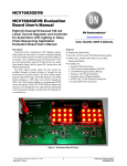
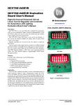
NCV7691GEVB
NCV7691 Current Controller
with Automotive LED Lamps
in Sequencing Application
Evaluation Board
User'sManual
http://onsemi.com
EVAL BOARD USER’S MANUAL
Description
Automotive turn signals are sometimes designed to
display an indicator in a fashion such that lights are activated
in a sequencing manner to show directional intent.
This evaluation note highlights the use of standard logic
integrated circuits with the NCV7691 devices to provide a
solution for a sequencing design. The system consists of the
LED current controllers (NCV7691 x 3), a voltage regulator
(NCV8664), a timer IC (NCV1455B), a shift register
(MC74HC164A), and a NAND gate (MC74HC20A).
The evaluation board has an on−board LED array to
highlight a sequencing solution for automotive indicators.
An additional 10−pin edge connector allows for connection
to external LEDs (often at higher current by modifying the
current programming resistors).
Features
In addition to the NCV7691 part features, this evaluation
board highlights the following:
• Sequencing Functionality
• Open Circuit Reporting
♦ Indicator On−board
♦ Connection for Off−board Communication
• External LED Load Connectivity
• Bright / Dim Switch for Easy Viewing
• 5 V Regulator Output
Figure 1. Board Top
© Semiconductor Components Industries, LLC, 2014
June, 2014 − Rev. 5
Figure 2. Board Bottom
1
Publication Order Number:
EVBUM2211/D
NCV7691GEVB
Basic Demonstration
Open Circuit Detection
Figure 3 provides a representation of the display feature
of this evaluation board.
1. When the board is powered, 3 sets of LED strings
are initialized in the off state.
2. The 1st string of LEDs turns on.
3. After a delay period, the 2nd string of LEDs turns
on while the 1st string remains illuminated.
4. After a similar delay period, the 3rd string of LEDs
turns on while the 1st and 2nd string remain
illuminated.
5. All 3 strings remain illuminated for an extended
period of time.
6. The progression is repeated as all 3 sets of LED
strings transition to the off state.
The NCV7691 utilizes the voltage feedback network to
the FB pin for detection of open circuit conditions to be
reported at the FLTS pin. An open circuit condition using
this board can be simulated by removing Jumpers J1, J2, and
J3. The open circuit is indicated at the on−board LED bar,
but J5 may be removed to route the signal off the board if
desired. Detection of open circuit conditions require
jumpers J8, J9, and J10 to be connected when using the
on−board LED array LED loads.
The low current setup with the LED array using supplied
board resistor values for R3, R7, and R8 of 8.2 W will
illuminate each segment of the LED array at 18 mA. The
drive capability of the NCV7691 to the base of the external
transistor has a value per the datasheet between 14 mA and
30 mA. An open circuit condition might fail to be detected
if all of the drive current is directed to the base of the BCP56
device to the emitter of the BCP56 device through to the
sense resistors on the FB pins (R3, R7, R8). e.g. If the drive
capability of the NCV7691 is 18 mA, and 18 mA is provided
to the base, the voltage at the FB pin will be at the regulation
voltage (150 mV) with or without an open circuit event. The
voltage generated on the FB pin will be high enough for the
system to think the device is regulating and no open circuit
exists. This is why three jumpers are provided on the demo
board (J8, J9, J10). Connecting these jumpers provides a
load directly to the base drive node to eliminate some of the
base drive so that an open circuit condition will be detected.
Figure 3. NCV7691 Sequencing
http://onsemi.com
2
NCV7691GEVB
Figure 4. Evaluation Board Schematic
EVALUATION BOARD SCHEMATIC
http://onsemi.com
3
NCV7691GEVB
THEORY OF OPERATION
The sequencing system design is comprised of all the
blocks shown in the diagram below. The Linear regulator
provides a 5 V regulated line to the logic ICs (Timer, Shift
Register, and NAND gate). The timer provides the clock for
the shift register, and the NAND gate provides the required
state to the NCV7691 pre−driver devices.
LOAD3
LOAD2
LOAD1
VPWR
R6, 680 W
R12, 680 W
R7, 680 W
Q1
BCP56
Q3
BCP56
Q2
BCP56
R3
R2
R8
To microprocessor
R4
VPWR
R10
R5
SC
VS
PWM BASE
M1
2N7002W
FB
C1 0.1 mF
FLTS
NTC
GND
NCV7691
VPWR
VS
SC
PWM BASE
FB
FLTS
NTC
VPWR
GND
SC
VS
NCV7691
PWM BASE
FB
FLTS
NTC
GND
NCV7691
Linear
Regulator
(NCV8664)
Timer
(NCV1455B)
Shift Register
(MC74HC164A)
NAND
Logic
(MC74HC20A)
Figure 5.
http://onsemi.com
4
NCV7691GEVB
LOGIC
through values 100, 110, 111, and 000. The following figure
displays the timing of these outputs relative to the clock
input.
The NCV1455B timer output is connected to the clock
input of the MC74HC164A shift register. At every rising
edge of clock, the shift register outputs QA, QB, and QC
change. In four clock pulses, the output QAQBQC cycles
Figure 6. Shift Register Clock Input and Parallel Data Outputs
This is also highlighted in the scope capture of Figure 7.
Figure 7. Shift Register (MC74HC164A) Outputs, Pin 3 (yellow), Pin 4 (pink), Pin 5 (blue)
The evaluation board includes three NCV7691 current
controller ICs that drive one LED string each. Shift register
outputs QA, QB, and QC are connected directly to the
NCV7691 PWM inputs. When the PWM signal goes high,
the driver output goes high and the LEDs turns on.
Therefore, when the shift register outputs a signal of 100,
LED1 is on. A shift register output of 110 corresponds to
LED1 and LED2 turning on, and a signal of 111 will turn all
three LEDs on. When QA, QB, and QC are all 0, all three
LEDs are off.
The MC74HC20A (NAND) device provides the logic
necessary to extend the timer when the 111 condition is
present in the shift register. The MC74HC20A interfaces to
the BSS84L PFET during this condition adding extra
capacitance (C7) in the timer circuit (NCV1455B).
Automotive turn signal applications frequently use this to
indicate a direction, and then hold the signal present for a
duration of time longer than the shifted signal.
http://onsemi.com
5
NCV7691GEVB
ABSOLUTE MAXIMUM RATINGS
The operation of the NCV7691 sequencer evaluation
board works as a standalone presentation for the customer
highlighting the sequencing function often used in
automotive turn signals. The on−board LED array is used for
situations where simplicity is needed. An additional
edge−connector can be used for alternative LEDs. Jumpers
J1, J2, and J3 provide the interface switch for the
edge−connector. Higher currents are assumed to be used
with the edge−connector, so extra care must be taken not to
reposition the jumpers for high currents through the
on−board LED array.
Table 1. ABSOLUTE MAXIMUM RATINGS
Rating
Value
Unit
−0.3 V (min), 45 (max)
V
LED Current Source (TP2, TP4, TP5) (Edge Connector)(BCP56)
1
A
LED Current Source max voltage (TP2, TP4, TP5) (Edge Connector)(BCP56)
80
V
Supply Voltage to board (TP1, VBB) (NCV8664)
Open Circuit Voltage (TP6, Open Circuit) (2N7002W)
60
V
Open Circuit Sink Current (TP6, Open Circuit) (2N7002W)
220
mA
Junction Temperature (NCV7691)
−40 to 150
°C
Ambient Temperature (Evaluation Board)
−40 to 105
°C
Stresses exceeding Maximum Ratings may damage the device. Maximum Ratings are stress ratings only. Functional operation above the
Recommended Operating Conditions is not implied. Extended exposure to stresses above the Recommended Operating Conditions may affect
device reliability.
Table 2. RECOMMENDED BOARD OPERATING CONDITIONS
Value
Min
Max
Unit
External Digital Supply Voltage (VBB)
7
16
V
LED Current Source(TP2, TP4, TP5)(Edge Connector)
(Note 1)
−
1
A
−40
150
°C
Rating
Junction Temperature (NCV7691)
1. Beta of the BCP56 external driver at the specified operating temperature must be considered when operating at high currents in order to
obtain the system design goals.
Table 3. PIN FUNCTION DESCRIPTION
Connector
Pin Number
Terminal Name
Power
TP1
Edge Connector
Pins 1 & 2
VBB
Power supply input voltage (14 V).
GND
GND
Ground.
TP2
Edge Connector
Pins 3 & 4
LED1
Connection to BCP56 collector current source output for U1
(NCV7691).
TP4
Edge Connector
Pins 5 & 6
LED2
Connection to BCP56 collector current source output for U2
(NCV7691).
TP5
Edge Connector
Pins 7 & 8
LED3
Connection to BCP56 collector current source output for U3
(NCV7691).
TP6
Open Circuit
Or’d connection from the 3 NCV7691 open circuit detection.
TP7
Vout (5 V)
Connection
Points
Test Points
Description
Connection to the NCV8664 5 V regulator output.
http://onsemi.com
6
NCV7691GEVB
Power supply connections.
Open Circuit jumper and post.
External LED edge connector.
Vout (5 V)
External LED post connections.
On−board / Off−board Jumpers.
External LED current
programming resistors.
Bright / Dim Control
Base Load Resistor Jumpers
Figure 8. Evaluation Board Highlights
OPERATIONAL GUIDELINES
Using the Evaluation Board with external LEDs
The material necessary to successfully use the
evaluation boards is listed below:
• NCV7691 Evaluation Board
• 14 V Power Supply Capable of driving 1 A.
1. Calculate the programming resistor value you need
by referring to the NCV7691/D datasheet.
a.) At nominal operating voltages the equation for
programming current is 0.15 V/Rx where Rx is the
equivalent resistance from the NCV7691 FB pin to
ground.
b.) On the board, using switch SW1 disengaged (DIM),
the resistors are R3 (for LED1), R7 (for LED2), and R8
(for LED3). When the switch is engaged (BRIGHT) a
resistor is put in parallel with the DIM resistor value.
These are R14 (for LED1), R15 (for LED2), and R16
(for LED3).
Connect a 14 V power supply to the power supply
connections. The board should start working immediately.
Evaluation Board Options
1. Open Circuit Jumper and Post. Allows
disconnection from the drain of the open circuit
indicator from the LED array to an external
connection.
2. External LED edge connector. Connection for use
with external LEDs. Note, the On−board /
Off−board jumpers should be moved to the right
for off−board connection. Reference the
NCV7691/D datasheet for details on choosing a
resistor value.
3. Bright / Dim Control. Controls a parallel
connection for a programming current resistor for
viewing ease.
4. External LED current programming resistors –
Current setting resistors for high current switched
in with the Bright / Dim dipswitch.
5. On−board / Off−board Jumpers. For setting the
board for use with the LED array or an external
LED via the edge connector.
6. External LED post connection. Optional
connection for external LEDs as an alternative to
the edge connector.
7. Vout (5 V). Connection to the 5 V regulator used
to power the on−board logic.
2. Once the resistors are mounted on the board, move
the jumpers from on−board to off−board (J1, J2,
and J3).
3. Connect your external LEDs cathode either
through the edge connector or the posts (TP2
[LED1], TP4 [LED2], and TP5[LED3]). The LED
anode (string) should be tied to a high voltage
(VBB suggested).
4. Connect a 14 V power supply to the power supply
connections. The board should start working
immediately.
http://onsemi.com
7
NCV7691GEVB
Table 4. JUMPER DESCRIPTION
Jumper #
Description
J1−J3
Directs current to on−board LED array or external
LED board via the edge connector.
Removing jumpers simulates an open circuit
condition.
J5
Removes open load indicator from LED array to
transistor source output (Q1) when jumper is
removed.
J8−J10
Adds loads (R10, R11, R12) to the bases of the
BCP56 transistors when the jumper is added for
use with light loads to allow for open load
detection.
Figure 9. NCV7691 Sequencing
BILL OF MATERIALS
Table 5. NCV7691 SEQUENCING EVALUATION BOARD BILL OF MATERIALS
Description
Value
Tolerance
Footprint
Manufacturer
Manufacturer
Part Number
Substitution
Allowed
Designator
QTY
U1, U2, U3
3
NCV7691 Current
Controller
−−−
−−−
SOIC−8
ON
Semiconductor
NCV7691D1R2G
No
U4
1
8−Bit Serial−Input/Parallel−Output Shift Register
−−−
−−−
SOIC−14
ON
Semiconductor
MC74HC164ADR2G
Yes
U8
1
Timer
−−−
−−−
SOIC−8
ON
Semiconductor
NCV1455BDR2G
Yes
U9
1
Dual 4−Input NAND Gate
−−−
−−−
SOIC−14
ON
Semiconductor
MC74HC20ADR2G
Yes
U10
1
Very Low Iq Low Dropout
Linear Regulator
−−−
−−−
DPAK
ON
Semiconductor
NCV8664DT50RKG
Yes
Q1
1
Small Signal MOSFET
−−−
−−−
SC−70 /
SOT−323
ON
Semiconductor
2N7002WT1G
Yes
Q2, Q3, Q4
3
NPN Silicon Epitaxial
Transistor
−−−
−−−
SOT−223
ON
Semiconductor
BCP56−10T1G
No
Q5
1
Single P. Channel Power
MOSFET
−−−
−−−
SOT−23−
3
ON
Semiconductor
BVSS84LT1G
Yes
R1, R2
2
10K Timer Resistor
10K
1%
0805
Vishay/Dale
CRCW080510K0FKEA
Yes
R4, R5, R6
3
10K Short Circuit Interface Resistor
10K
1%
0805
Vishay/Dale
CRCW080510K0FKEA
Yes
R13
1
1K Open−circuit LED
drive resistor
1K
1%
0805
Vishay/Dale
CRCW08051K00FKEA
Yes
R3, R7, R8
3
8.2 W LED array
programming resistors
8.2
1%
0805
Vishay/Dale
CRCW08058R20FKEA
Yes
R9
1
1 W Shift register pull−up
1
1%
0805
Vishay/Dale
CRCW08051R00FKEA
Yes
R14, R15,
R16
3
High Current
programming resistor
Customer
Defined
1%
1206
Vishay/Dale
Customer Defined
Yes
R17
1
620 W 5 V LED drive
resistor
620
1%
0805
Vishay/Dale
CRCW0805620RFKEA
Yes
C1
1
Regulator Output
Capacitor
10 mF,
10 V
10%
1206
Murata Electronics
North America
GRM31CR61A106KA01L
Yes
C2
1
Timer Capacitor
10 mF,
10 V
10%
1206
Murata Electronics
North America
GRM31CR61A106KA01L
Yes
C3
1
Supply Line Filter
Capacitor
0.1 mF,
50 V
10%
0805
Murata Electronics
North America
GRM21BR71H104KA01L
Yes
C4
1
Timer Control Voltage
Capacitor
0.01 mF,
50 V
10%
0805
Murata Electronics
North America
GRM216R71H103KA01D
Yes
http://onsemi.com
8
NCV7691GEVB
Table 5. NCV7691 SEQUENCING EVALUATION BOARD BILL OF MATERIALS
Designator
QTY
Description
Value
Tolerance
Manufacturer
Part Number
Substitution
Allowed
Footprint
Manufacturer
C5
1
Fault Timer Capacitor
0.1 mF,
50 V
10%
0805
Murata Electronics
North America
GRM21BR71H104KA01L
Yes
C6
1
Power Supply Input Filter
Capacitor
0.1 mF,
50 V
10%
0805
Murata Electronics
North America
GRM21BR71H104KA01L
Yes
C7
1
Extended Timer Capacitor
33 mF
20%
1206
TDK Corporation
C3216X5R1A336M160AB
Yes
D1
1
5 V LED Indicator
−−−
−−−
0805
Lite−On Inc
LTST−C171GKT
Yes
J1, J2, J3
3
On−Board / Off−Board
Jumper
−−−
−−−
JP3
Molex Connector
Corporation
22−28−4033
Yes
J4
1
LED Array Socket
−−−
−−−
DIP20
3M
4820−3000−CP
Yes
−−−
1
LED Array
−−−
−−−
DIP20
Avago
HDSP−4840
Yes
J5
1
Open Circuit Jumper
−−−
−−−
JMP
Molex Connector
Corporation
22−28−4023
Yes
J6
1
10−pin Edge Connector
−−−
−−−
EDGECO
NN10
Sullins Connector
Solutions
EBC05DRAS
Yes
J7
1
Supply Input Terminal
−−−
−−−
MKDSN2
Phoenix Contact
1729128
Yes
SW1
1
Bright / Dim Switch
−−−
−−−
DIP6
Grayhill Inc
78G01ST
Yes
TP1−TP8
8
Test Point
−−−
−−−
TP
Keystone
Electronics
5010
Yes
ON Semiconductor and
are registered trademarks of Semiconductor Components Industries, LLC (SCILLC). SCILLC owns the rights to a number of patents, trademarks,
copyrights, trade secrets, and other intellectual property. A listing of SCILLC’s product/patent coverage may be accessed at www.onsemi.com/site/pdf/Patent−Marking.pdf. SCILLC
reserves the right to make changes without further notice to any products herein. SCILLC makes no warranty, representation or guarantee regarding the suitability of its products for any
particular purpose, nor does SCILLC assume any liability arising out of the application or use of any product or circuit, and specifically disclaims any and all liability, including without
limitation special, consequential or incidental damages. “Typical” parameters which may be provided in SCILLC data sheets and/or specifications can and do vary in different applications
and actual performance may vary over time. All operating parameters, including “Typicals” must be validated for each customer application by customer’s technical experts. SCILLC
does not convey any license under its patent rights nor the rights of others. SCILLC products are not designed, intended, or authorized for use as components in systems intended for
surgical implant into the body, or other applications intended to support or sustain life, or for any other application in which the failure of the SCILLC product could create a situation where
personal injury or death may occur. Should Buyer purchase or use SCILLC products for any such unintended or unauthorized application, Buyer shall indemnify and hold SCILLC and
its officers, employees, subsidiaries, affiliates, and distributors harmless against all claims, costs, damages, and expenses, and reasonable attorney fees arising out of, directly or indirectly,
any claim of personal injury or death associated with such unintended or unauthorized use, even if such claim alleges that SCILLC was negligent regarding the design or manufacture
of the part. SCILLC is an Equal Opportunity/Affirmative Action Employer. This literature is subject to all applicable copyright laws and is not for resale in any manner.
PUBLICATION ORDERING INFORMATION
LITERATURE FULFILLMENT:
Literature Distribution Center for ON Semiconductor
P.O. Box 5163, Denver, Colorado 80217 USA
Phone: 303−675−2175 or 800−344−3860 Toll Free USA/Canada
Fax: 303−675−2176 or 800−344−3867 Toll Free USA/Canada
Email: [email protected]
N. American Technical Support: 800−282−9855 Toll Free
USA/Canada
Europe, Middle East and Africa Technical Support:
Phone: 421 33 790 2910
Japan Customer Focus Center
Phone: 81−3−5817−1050
http://onsemi.com
9
ON Semiconductor Website: www.onsemi.com
Order Literature: http://www.onsemi.com/orderlit
For additional information, please contact your local
Sales Representative
EVBUM2211/D