1
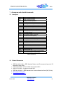
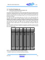
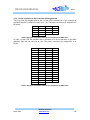
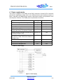
FM480 USER MANUAL
V1.0
FM480
User Manual
4DSP Inc.
1757 Fox Run road, Reno, NV 89509-0907, USA.
Email: [email protected]
This document is the property of 4DSP Inc. and may not be copied nor communicated to a
third party without the written permission of 4DSP Inc.
© 4DSP Inc. 2006
FM480 USER MANUAL
V1.0
Revision History
Date
03-22-06
March 2006
Revision
Initial release
Version
1.0
FM480 User Manual
www.4dsp.com
-2-
FM480 USER MANUAL
V1.0
Table of Contents
1
2
3
4
5
6
7
8
Acronyms and related documents................................................................................4
1.1
Acronyms..................................................................................................................4
1.2
Related Documents ..................................................................................................4
1.3
General description ..................................................................................................5
Installation.......................................................................................................................6
2.1
Requirements and handling instructions ..................................................................6
2.2
Firmware and software .............................................................................................6
Design..............................................................................................................................6
3.1
FPGA devices...........................................................................................................6
3.1.1
Virtex-II Pro device A ........................................................................................6
3.1.2
Virtex-4 device B...............................................................................................9
3.2
FPGA devices configuration ...................................................................................10
3.2.1
Flash storage ..................................................................................................10
3.2.2
CPLD device...................................................................................................10
3.2.3
JTAG...............................................................................................................12
3.3
Clocks.....................................................................................................................12
3.4
Memory resources ..................................................................................................13
3.4.1
QDR2 SRAM ..................................................................................................13
3.4.2
DDR2 SDRAM ................................................................................................13
3.5
Front Panel IO daughter card .................................................................................14
3.5.1
Virtex-4 device B to I/O front Panel daughter card .........................................14
(only available with daughter card purchase) .................................................................14
3.5.2
Power connection to the front panel I/O daughtercard ...................................16
Power requirements .....................................................................................................17
4.1
External power connector .......................................................................................18
Environment..................................................................................................................19
5.1
Temperature ...........................................................................................................19
5.2
Convection cooling .................................................................................................19
5.3
Conduction cooling .................................................................................................19
Safety.............................................................................................................................19
EMC................................................................................................................................19
Warranty ........................................................................................................................19
March 2006
FM480 User Manual
www.4dsp.com
-3-
FM480 USER MANUAL
V1.0
1 Acronyms and related documents
1.1
Acronyms
ADC
DAC
DCI
DDR
DSP
EPROM
FBGA
FPDP
FPGA
JTAG
LED
LVTTL
LVDS
LSB
LVDS
MGT
MSB
PCB
PCI
PLL
PMC
QDR
SDRAM
SRAM
Analog to Digital Converter
Digital to Analog Converter
Digitally Controlled Impedance
Double Data Rate
Digital Signal Processing
Erasable Programmable Read-Only Memory
Fineline Ball Grid Array
Front Panel Data Port
Field Programmable Gate Array
Join Test Action Group
Light Emitting Diode
Low Voltage Transistor Logic level
Low Differential Data Signaling
Least Significant Bit(s)
Low Voltage Differential Signaling
Multi-Gigabit Transceiver
Most Significant Bit(s)
Printed Circuit Board
Peripheral Component Interconnect
Phase Locked Loop
PCI Mezzanine Card
Quadruple Data rate
Synchronous Dynamic Random Access memory
Synchronous Random Access memory
Table 1: Glossary
1.2
Related Documents
•
•
•
•
•
•
IEEE Std 1386.1-2001 : IEEE Standard Physical and Environmental Layers for PCI
Mezzanine Cards (PMC).
ANSI/VITA 39-2003 : PCI-X for PMC and Processor PMC.
ANSI/VITA 20-2001 : Conduction Cooled PMC.
IEEE Std 1386-2001 : IEEE Standard for a Common Mezzanine Card (CMC) Family.
Xilinx Virtex-4 user guide
Xilinx PCI-X core datasheet
March 2006
FM480 User Manual
www.4dsp.com
-4-
FM480 USER MANUAL
1.3
V1.0
General description
The FM480 is a high performance PMC dedicated to digital signal processing applications
with high bandwidth and complex algorithms requirements. PCI-X and PCI backward
compatible, the FM480 offers various interfaces, fast on-board memory resources and one
Virtex-4 FPGA. It can be utilized, for example, to accelerate frequency-domain algorithms
with off-the-shelf Intellectual Property cores for applications that require the highest level of
performances. The FM480 is mechanically and electrically compliant to the standard and
specifications listed in section 1.2 of this document.
Figure 1: FM480 block diagram
March 2006
FM480 User Manual
www.4dsp.com
-5-
FM480 USER MANUAL
V1.0
2 Installation
2.1
Requirements and handling instructions
•
The FM480 must be installed on a motherboard compliant to the IEEE Std 1386-2001
standard for 3.3V PMC
Do not flex the board
Observe SSD precautions when handling the board to prevent electrostatic
discharges.
Do not install the FM480 while the motherboard is powered up.
•
•
•
2.2
Firmware and software
Drivers, API libraries and a program example working in combination with a pre-programmed
firmware for both FPGAs are provided. The FM480 is delivered with an interface to the Xilinx
PCI core in the Virtex-II Pro device and an example VHDL design in the Virtex-4 device so
users can start performing high bandwidth data transfers over the PCI bus right out of the
box. For more information about software installation and FPGA firmware, please refer the
FM480 Get Started Guide.
3 Design
3.1
FPGA devices
The Virtex-II Pro and Virtex-4 FPGA devices interface to the various resources on the FM480
as shown on Figure 1. They also interconnect to each other via 86 general purpose pins and
2 clock pins.
3.1.1
3.1.1.1
Virtex-II Pro device A
Virtex-II Pro device A family and package
The Virtex-II Pro device is a XC2VP7 in a Fineline Ball Grid array with 672 balls (FF672).
3.1.1.2
Power PC embedded processor
One IBM PowerPC RISC processor cores is available in the Virtex-II Pro device A. This core
can be used to execute C based algorithms and control the logic resources implemented in
the FPGA.
3.1.1.3
Virtex-II Pro device A external memory interfaces
The Virtex-II Pro device A is connected to two 128Mbytes SDRAM devices with 16-bit data
bus width. These memory resources can be used by the PowerPC core or can serve as data
buffers.
3.1.1.4
PCI interface
The Virtex-II Pro device A interfaces directly to the PCI bus via the PMC P1n, P2n and P3n
connectors. An embedded PCI core from Xilinx is used to communicate over the PCI bus
with the host system on the motherboard. PCI-X 64-bit 66MHz/133MHz, PCI 64-bit 66MHz
March 2006
FM480 User Manual
www.4dsp.com
-6-
FM480 USER MANUAL
V1.0
and PCI 32-bit 33MHz are supported on the FM480. The bus type must be communicated at
the time of the order so the right Virtex-II Pro firmware can be loaded into the flash prior
delivery.
The following performances have been recorded with the FM480 transferring data on the
bus:
¾ PCI-X 64-bit 133MHz: 650Mbytes/s sustained
¾ PCI-X 64-bit 66MHz: 450Mbytes/s sustained
¾ PCI 32-bit 33MHz: 120Mbytes/s sustained
3.1.1.5
LED
Four LEDs are connected to the Virtex-II Pro device. In the default FPGA firmware, the LEDs
are driven by the Virtex-4 device via the Virtex-II Pro / Virtex-4 interface.
The LEDs are located on side 2 of the PCB in the front panel area.
March 2006
FM480 User Manual
www.4dsp.com
-7-
FM480 USER MANUAL
3.1.1.6
V1.0
Pn4 user I/O connector
The 64-pin Pn4 connector is wired to the Virtex-II Pro device A. All signals are user-defined
3.3V LVTLL.
Connector
pin
1
3
5
7
9
11
13
15
17
19
21
23
25
27
29
31
33
35
37
39
41
43
45
47
49
51
53
55
57
59
61
63
Signal
name
Pn4_IO0
Pn4_IO2
Pn4_IO4
Pn4_IO6
Pn4_IO8
Pn4_IO10
Pn4_IO12
Pn4_IO14
Pn4_IO16
Pn4_IO18
Pn4_IO20
Pn4_IO22
Pn4_IO24
Pn4_IO26
Pn4_IO28
Pn4_IO30
Pn4_IO32
Pn4_IO34
Pn4_IO36
Pn4_IO38
Pn4_IO40
Pn4_IO42
Pn4_IO44
Pn4_IO46
Pn4_IO48
Pn4_IO50
Pn4_IO52
Pn4_IO54
Pn4_IO56
Pn4_IO58
Pn4_IO60
Pn4_IO62
FPGA
pin
P2
P4
P6
R1
R3
R5
P8
T1
T3
T5
R7
T8
U1
U3
U5
V2
V4
V6
W1
W3
W5
Y1
Y3
Y5
N7
N5
N3
AB3
AC1
AD1
AE1
AC3
FPGA
pin
P3
P5
P7
R2
R4
R6
R8
T2
T4
T6
T7
U7
V1
U4
U6
V3
V5
V7
W2
W4
W6
AA1
Y4
Y6
N6
N4
N2
AB4
AC2
AD2
AF2
AD4
Signal
name
Pn4_IO1
Pn4_IO3
Pn4_IO5
Pn4_IO7
Pn4_IO9
Pn4_IO11
Pn4_IO13
Pn4_IO15
Pn4_IO17
Pn4_IO19
Pn4_IO21
Pn4_IO23
Pn4_IO25
Pn4_IO27
Pn4_IO29
Pn4_IO31
Pn4_IO33
Pn4_IO35
Pn4_IO37
Pn4_IO39
Pn4_IO41
Pn4_IO43
Pn4_IO45
Pn4_IO47
Pn4_IO49
Pn4_IO51
Pn4_IO53
Pn4_IO55
Pn4_IO57
Pn4_IO58
Pn4_IO59
Pn4_IO60
Connector
pin
2
4
6
8
10
12
14
16
18
20
22
24
26
28
30
32
34
36
38
40
42
44
46
48
50
52
54
56
58
60
62
64
Table 2 : Pn4 pin assignment
March 2006
FM480 User Manual
www.4dsp.com
-8-
FM480 USER MANUAL
3.1.2
3.1.2.1
V1.0
Virtex-4 device B
Virtex-4 device B family and package
The Virtex-4 device B is dedicated to Digital Signal Processing applications and can be
chosen from the SX or LX family devices. Its package is based on Fineline Ball Grid array
with 1148 balls. In terms of logic and dedicated DSP resources, it is available in 5 different
sizes: SX55, LX40, LX60, LX80, LX100 and LX160. The speed grade and temperature
operating range can be chosen upon customer requirements.
3.1.2.2
Virtex-4 device B external memory interfaces
The Virtex-4 device B interfaces to four 8Mbytes QDR2 SRAM devices with 32-bit data bus,
Please note that the four QDR2 SRAM devices are only available with the LX80, LX100 and
LX160 devices. For smaller Virtex-4 FPGAs (LX40, LX60 and SX55) only three QDR2 SRAM
devices are connected to the FPGA.
3.1.2.3
Virtex-4 device B interface to Front Panel daughter card
The Virtex-4 device B interfaces to the front panel daughter card on the FM480 via a high
speed connector. 120 I/Os are available from the FPGA to/from the daughter card.
Refer to the Front Panel I/O section of this document for more details about the daughter
card connector electrical characteristics.
March 2006
FM480 User Manual
www.4dsp.com
-9-
FM480 USER MANUAL
3.2
V1.0
FPGA devices configuration
3.2.1 Flash storage
The FPGA firmware is stored on board in a flash device. The 256Mbit device is partly
used to store the configuration for both FPGAs. In the default CPLD firmware
configuration, the Virtex-II Pro and Virtex-4 devices are directly configured from flash if a
valid bitstream is stored in the flash for each FPGA. The flash is pre-programmed in
factory with the default Virtex-II pro firmware and a Virtex-4 firmware example.
Figure 2 : Configuration circuit
3.2.2 CPLD device
As shown on Figure 2, a CPLD is present on board to interface between the flash device and
the FPGA devices. It is of type CoolRunner-II. The CPLD is used to program and read the
flash. The data stored in the flash are transferred from the host motherboard via the PCI bus
to the Virtex-II Pro device A and then to the CPLD that writes the required bit stream to the
storage device. A 50 MHz clock connects to the CPLD and is used to generate the
configuration clock sent to the FPGA devices. At power up, if the CPLD detects that an
FPGA configuration bitstream is stored in the flash for both FPGA devices, it will start reading
programming the devices in SelecMap mode.
Do NOT reprogram the CPLD without 4DSP approval
The CPLD configuration is achieved by loading with a Xilinx download cable a bitstream from
a host computer via the JTAG connector. The FPGA devices configuration can also be
performed using the JTAG.
March 2006
FM480 User Manual
www.4dsp.com
- 10 -
FM480 USER MANUAL
3.2.2.1
V1.0
Jumper
A Jumper (J1) is connected to the CPLD and is used to choose the FPGA configuration
scheme. The jumper is located next to the Pn3 connector. The Jumper positions are defined
as follows.
ON
JTAG chain enabled for FPGAs configuration, FPGAs are not configured
from the flash
OFF
Configuration from the flash enabled if valid FPGA bitstreams are stored in
the flash
OFF to
ON
The Virtex-II Pro safety configuration is loaded from the Flash into the
Virtex-II Pro. This scheme is to be used only to allow a user to reprogram
the flash with valid FPGA bitstreams.
Table 3: Jumper
3.2.2.2
LED and board status
Four LEDs connect to the CPLD and give information about the board status.
LED 1
LED 2
LED 3
Blinking
FPGA A or B bitstream or user_ROM_register is currently
being written to the flash
ON
FPGA A not configured
OFF
FPGA A configured
Blinking
FPGA A or B bitstream or user_ROM_register is currently
being written to the flash
ON
FPGA B not configured
OFF
FPGA devices configured
Blinking
The Virtex-II Pro FPGA has been configured with the safety
configuration bitstream programmed in the flash at factory.
Please write a valid Virtex-II Pro bitstream in the flash.
ON
Flash is busy writing or erasing
OFF
Flash device is not busy
ON
CRC error. Presumably a wrong or corrupted FPGA bitstream
has been written to the flash. Once on this LED remains on
OFF
No CRC error detected
LED 4
Table 4: LED board status
The LEDs are located on side 2 of the PCB in the front panel area.
March 2006
FM480 User Manual
www.4dsp.com
- 11 -
FM480 USER MANUAL
V1.0
3.2.3 JTAG
A JTAG connector is available on the FM480 for configuration purposes. The JTAG can also
be used to debug the FPGA design with the Xilinx Chipscope.
Please note that three Xilinx devices will be detected in the JTAG chain. The JTAG
connector is located on side 1 of the PCB in front of Pn3.
The JTAG connector pinout is as follows:
Pin #
1
2
3
Signal
1.8V
GND
TCK
Signal
TMS
TDI
TDO
Pin #
4
5
6
Table 5 : JTAG pin assignment
3.3
Clocks
A 50MHz oscillator on-board connects to a low skew 1:4 clock buffer (ICS553). Each FPGA
device and the CPLD receive this 50MHz clock. By using the DCM resources inside the
FPGA, clocks are generated for the various interfaces on board. Figure 2 shows how the
clocks signals between the FPGAs and the CPLD are connected. The IO pin number is
provided for each device.
Figure 3 : Clocks
March 2006
FM480 User Manual
www.4dsp.com
- 12 -
FM480 USER MANUAL
3.4
V1.0
Memory resources
3.4.1 QDR2 SRAM
Four independant QDR2 SRAM devices are connected to the Virtex-4 device B. The QDR2
SRAM devices available on the FM480 are 2M words deep (8Mbytes per memory device).
Please note that only three QDR SRAM devices are available to the user if the XC4VLX40,
XC4VLX60 or XC4VSX55 FPGA device is mounted on board.
3.4.2 DDR2 SDRAM
Two 8-bit DDR2 SDRAM devices are connected to Virtex-II Pro device A. The two memories
share a common address bus and can be considered as a single DDR2 SDRAM bank of
128Mbytes with a 16-bit data bus width. These memory resources are primarily intended to
be accessed by the PowerPC processor in the Virtex-II Pro device A. They can however be
used for any purpose.
March 2006
FM480 User Manual
www.4dsp.com
- 13 -
FM480 USER MANUAL
3.5
V1.0
Front Panel IO daughter card
3.5.1
Virtex-4 device B to I/O front Panel daughter card
(only available with daughter card purchase)
The Virtex-4 device B interfaces to a 120-pin connector placed in the Front panel I/O area
(on both side 1 and side 2 of the PCB). It serves as a base for a daughter card and offers I/O
diversity to the FM480 PMC. On side 2 of the PCB, the connectors and mounting holes
placement complies with the SLB standard except for the 2.5V mounting holes that are not
present on this module.
The FPGA I/O banks are powered either by 1.8V, 2.5V or 3.3V. Using the Xilinx DCI
termination options to match the signals impedance allows many electrical standards to be
supported by this interface. All signals are routed as 100-ohm LVDS pairs. The VRP and
VRN pins on the I/O banks connected to the daughter card connector are respectively pulled
up and pulled down with 50-ohm resistors in order to ensure optimal performances when
using the Xilinx DCI options. The VREF pins are connected to 0.85V for DDR2 DCI
terminations. Please, contact 4DSP Inc. for more information about the daughter card types
available.
The 120-pin Samtec connector pin assignment is as follows. All signals are shown as LVDS
pairs in the table but they can be used for any standard that does not breach the electrical
rules of the Xilinx I/O pad.
Connector
pin
1
3
5
7
9
11
13
15
17
19
21
23
25
27
29
31
Signal
Name
FP_P0
FP_N0
FP_P2(2)
FP_N2(2)
FP_P4
FP_N4
FP_P6
FP_N6
FP_P8
FP_N8
FP_P10(2)
FP_N10(2)
FP_P12
FP_N12
FP_P14
FP_N14
FPGA
pin
W24
Y24
AA25
AA26
AB30
AA30
AB22
AB23
AC29
AC30
AD34
AC34
AE29
AD29
AE33
AE34
FPGA
pin
AA23
AA24
AA28
AA29
AC28
AB28
AD27
AC27
AC32
AC33
AE32
AD32
AF31
AE31
AF33
AF34
Signal
name
FP_P1
FP_N1
FP_P3
FP_N3
FP_P5
FP_N5
FP_P7
FP_N7
FP_P9
FP_N9
FP_P11
FP_N11
FP_P13
FP_N13
FP_P15
FP_N15
Connector
pin
2
4
6
8
10
12
14
16
18
20
22
24
26
28
30
32
33
FP_P16(1)
AH19
AF29
FP_P17(2)
34
35
(1)
AH18
AF30
(2)
36
37
(1)
FP_P18
AG18
AG30
FP_P19
38
39
FP_N18(1)
AG17
AG31
FP_N19
40
FP_N16
FP_N17
Table 6 : Front Panel IO daughter card pin assignment Bank A
(1)
Connected to a global clock pin on the FPGA. LVDS output not supported.
Connected to a regional clock pin on the FPGA. LVDS output not supported.
(2)
March 2006
FM480 User Manual
www.4dsp.com
- 14 -
FM480 USER MANUAL
Connector
pin
41
43
45
47
49
51
53
55
57
59
61
63
65
67
69
71
73
75
77
79
81
83
85
87
89
91
93
95
97
99
101
103
105
107
109
111
113
115
117
119
Differential
FP_P20
FP_N20
FP_P22
FP_N22
FP_P24(2)
(2)
FP_N24
FP_P26
FP_N26
FP_P28
FP_N28
FP_P30
FP_N30
FP_P32
FP_N32
FP_P34
FP_N34
FP_P36(2)
3.3V/2.5V/1.8V
3.3V/2.5V/1.8V
3.3V/2.5V/1.8V
FP_P37
FP_N37
FP_P39
FP_N39
FP_P41
FP_N41
FP_P43
FP_N43
FP_P45(2)
FP_N45(2)
FP_P47
FP_N47
FP_P49
FP_N49
FP_P51
FP_N51
(1)
FP_P53
FP_N53(1)
(1)
FP_P55
FP_N55(1)
V1.0
FPGA
pin
AG32
AG33
AH32
AH33
AK31
AK32
AL33
AL34
AM32
AM33
AM30
AL30
AK29
AJ29
AP29
AN29
AG27
FPGA
pin
AJ34
AH34
AJ30
AH30
AK33
AK34
AM31
AL31
AP30
AN30
AH28
AH29
AL28
AL29
AN28
AM28
AG28
AF28
AE27
AM26
AM27
AP25
AP26
AG25
AG26
AL24
AL25
AP24
AN24
AG23
AF24
AL23
AM23
AJ17
AH17
AE17
AE16
AJ27
AH27
AP27
AN27
AL26
AK26
AF26
AE26
AN25
AM25
AK24
AJ24
AK22
AK23
AN22
AN23
AP21
AP22
AK21
AL21
Differential
FP_P21
FP_N21
FP_P23
FP_N23
FP_P25
FP_N25
FP_P27
FP_N27
FP_P29
FP_N29
FP_P31
FP_N31
FP_P33
FP_N33
FP_P35(2)
FP_N35(2)
FP_N36(2)
Vbatt (3)
0.9V
3.3V/2.5V/1.8V
FP_P38
FP_N38
FP_P40
FP_N40
FP_P42
FP_N42
FP_P44
FP_N44
FP_P46
FP_N46
FP_P48
FP_N48
FP_P50
FP_N50
FP_P52
FP_N52
FP_P54
FP_N54
FP_P56
FP_N56
Connector
pin
42
44
46
48
50
52
54
56
58
60
62
64
66
68
70
72
74
76
78
80
82
84
86
88
90
92
94
96
98
100
102
104
106
108
110
112
114
116
118
120
Table 7 : Front Panel IO daughter card pin assignment Bank B and C
(1)
Connected to a global clock pin on the FPGA. LVDS output not supported.
Connected to a regional clock pin on the FPGA. LVDS output not supported.
(3)
Vbatt is connected to Virtex-II Pro device A and Virtex-4 device B Vbatt pin.
(2)
March 2006
FM480 User Manual
www.4dsp.com
- 15 -
FM480 USER MANUAL
V1.0
3.5.2 Power connection to the front panel I/O daughtercard
The Front Panel I/O daughter card on side 1 of the PCB is powered via a 7-pin connector of
type BKS (Samtec). Each pin can carry up to 1.5A. The power connector’s pin assignment is
as follows.
Pin #
1
3
5
7
Signal
+3.3V
+5V
+12V
-12V
Signal
+3.3V
GND
GND
Pin #
2
4
6
Table 8: Daughter card power connector pin assignment on PMC side 1
On side 2 of the PCB, the daughter card is powered via a 33-pin connector of type BKS
(Samtec). Each pin can carry up to 1.5A. The power connector’s pin assignment is as
follows.
Pin #
1
3
5
7
9
11
13
15
17
19
21
23
25
27
29
31
33
Signal
+3.3V
+3.3V
+3.3V
+3.3V
+5V
+5V
+5V
+5V
+12V
+12V
-12V
-12V
GND
reserved
reserved
reserved
GND
Signal
GND
GND
GND
GND
GND
GND
GND
GND
GND
GND
GND
GND
reserved
reserved
reserved
reserved
Pin #
2
4
6
8
10
12
14
16
18
20
22
24
26
28
30
32
Table 9: Daughter card power connector pin assignment on PMC side 2
March 2006
FM480 User Manual
www.4dsp.com
- 16 -
FM480 USER MANUAL
V1.0
4 Power requirements
The Power is supplied to the FM480 via the PMC connectors. Several DC-DC converters
generate the appropriate voltage rails for the different devices and interfaces present on
board. Optionally, the FM480 can be used as a stand alone module and is powered via the
external power connector. The FM480 power requirements are as follow.
Device/Interface
Voltage
Maximum current
DCI and memory reference voltage
0.85V
0.5 A
Virtex-4 device B core
1.2V
12A
Virtex-II Pro device A core
1.5V
6A
QDR2, DDR2 SDRAM core and I/O banks,
Virtex-4 abd Virtex-II Pro devices I/O banks
1.8V
10A
Virtex-4 device B I/O bank connected to the
front panel daughter card
1.8V/2.5/3.3V
1.5A
Virtex-II Pro device A I/O bank connected to
the PCI bus, Flash, CPLD, front Panel I/O
daughter card
3.3V
2A
Front Panel IO daughter card
5V
1A
Front Panel IO daughter card
12V
0.5A
Front Panel IO daughter card
-12V
0.5A
Table 10 : Power supply
Figure 4 : Power supply
March 2006
FM480 User Manual
www.4dsp.com
- 17 -
FM480 USER MANUAL
V1.0
An ADT7411 device is used to monitor the power on the different voltage rails as well as the
temperature. The ADT7411 data are constantly passed to the Virtex-II Pro device.
Measurements can be accessed from the host computer via the PCI bus. A software utility
delivered with the board allows the monitoring of the voltage on the 2.5V, 1.8V, 1.2V and
0.85V rails. It also displays the Virtex-4 junction temperature.
4.1
External power connector
An external power connector (J2) is available on side 2 of the PMC, next to the PMC
connectors. It is used to power the board when it is in stand alone mode. This is a right
angled connector and it will be mounted on board only if the card is ordered in its stand alone
version (FM480-SA). The height and placement of this connector on the PCB breaches the
PMC specifications and the module should not be used in an enclosed chassis compliant to
PMC specifications if the external power connector is present on board.
Do not connect an external power source to J1 if the board is powered via the
PMC connectors. Doing so will result in damaging the board.
The external power connector is of type Molex 43045-1021. Each circuit can carry a
maximum current of 5A. The connector pin assignment is as follows:
Pin #
1
3
5
7
9
Signal
3.3V
5V
GND
GND
-12V
Signal
3.3V
5V
GND
GND
12V
Pin #
2
4
6
8
10
Table 11 : External power connector pin assignment
March 2006
FM480 User Manual
www.4dsp.com
- 18 -
FM480 USER MANUAL
V1.0
5 Environment
5.1
Temperature
Operating temperature
• 0°C to +60°C (Commercial)
• -40°C to +85°C (Industrial)
Storage temperature:
• -40°C to +120°C
5.2
Convection cooling
600LFM minimum
5.3
Conduction cooling
The FM480 can optionally be delivered as conduction cooled PMC. The FM480 is compliant
to ANSI/VITA 20-2001 standard for conduction cooled PMC.
6 Safety
This module presents no hazard to the user.
7 EMC
This module is designed to operate from within an enclosed host system, which is build to
provide EMC shielding. Operation within the EU EMC guidelines is not guaranteed unless it
is installed within an adequate host system. This module is protected from damage by fast
voltage transients originating from outside the host system which may be introduced through
the system.
8 Warranty
Hardware
Software/Firmware
Basic Warranty (included)
1 Year from Date of Shipment
90 Days from Date of Shipment
Extended Warranty (optional)
2 Years from Date of Shipment
1 Year from Date of Shipment
March 2006
FM480 User Manual
www.4dsp.com
- 19 -