1
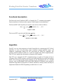
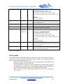
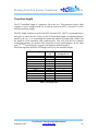
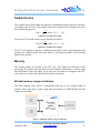
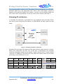
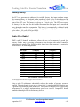
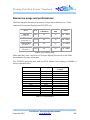
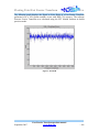
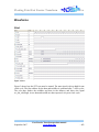
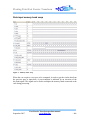
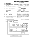
Floating Point Fast Fourier Transform V2.6 User manual Introduction The Fast Fourier Transform (FFT) is an efficient algorithm for computing the Discrete Fourier Transform (DFT). This Intellectual Property (IP) core was designed to offer very fast transform times while keeping an IEEE-754 floating point accuracy at all computational stages. 4DSP’s core is the fastest and the most efficient available in the FPGA world. Based on a radix-32 architecture, it also saves memory resources compared to other floating point cores available on the market. Features This IP core targets the following devices: Xilinx: Virtex-IITM, Virtex-II ProTM, Spartan-3TM and Virtex-4TM Altera: StratixTM, Cyclone-IITM and StratixIITM Forward and inverse complex FFT Transform sizes: 2m with m = 8 to 20 (256, 512, 1024, …, 1M points) Arithmetic type : floating point Data formats IEEE-754 24-bit mantissa, 8-bit exponent, 2’s complement 14-bit mantissa, 8-bit exponent, 2’s complement Any mantissa and exponent precision upon request Configurable on the fly forward or inverse operation Configurable on the fly transform length Fully functional VHDL testbench and the related Matlab functions delivered along the FFT/IFFT core for simulation purposes and specific performance characterization. September 2007 Fast Fourier Transform product manual www.4dsp.com -1- Floating Point Fast Fourier Transform V2.6 Functional description The Discrete Fourier Transform (DFT), of length N (N=2m), calculates the sampled Fourier transform of a discrete-time sequence with N points evenly distributed. The forward DFT with N points of a sequence x(n) can be written as follows: N 1 X (k ) n 0 x (n ) e j 2nk N with k = 0, 1, …, N-1 Equation 1: DFT The inverse DFT is given by the following equation: j 2nk 1 N 1 x ( n ) k 0 X ( k ) e N with n = 0, 1, …, N-1 N Equation 2 : Inverse DFT Algorithm The FFT core uses a decomposition of radix-2 butterflies for computing the DFT. With 5 butterflies in series, the processing of the transform requires log32(N) stages. All arithmetic computations during the FFT processing are IEEE-754 compliant. The software model available for this core is a bit true model of the FPGA implementation. This FFT core employs the decimation in frequency (DIF) method. This FFT core is designed for FFT computation larger or equal to 256 points and up to 1M points. Since FPGAs memory resources are limited and relatively small, the memory banks used for the processing of the transform are not integrated in the core. External memory, such as QDR SRAM, ZBT RAM, DDR SDRAM or SDRAM is most suited for transforms larger than 16384 points. For shorter transforms, memory banks can likely be implemented inside the FPGA depending on which device is used. September 2007 Fast Fourier Transform product manual www.4dsp.com -2- Floating Point Fast Fourier Transform V2.6 Data format This core is compliant to the IEEE-754 standard for Binary floating-point arithmetic. There is however one restriction regarding the optional denormalized numbers of this standard that are not supported by the Floating Point FFT core. Therefore, when intermediate calculations and results data are very small there might be some differences between the values generated by the core and 4DSP’s GUI. Please note however that the denormalized numbers option can be turned off on many processors. Other data formats available for this core are coded in 2’s complement for both the mantissa and exponent. The 8-bit exponent ranges from -128 to 127 The p-bit mantissa ranges from -2p-1 to 2p-1-1 The exponent bit width is noted Ebw. The mantissa bit width is noted Mbw. Parameters and Ports definitions Parameter name addr_width type Value Description integer ≥ 8 and ≤ 20 Address width. This parameter (also noted Abw) indicates the width of the address bus for twiddle factors and data. If N is the maximum transform length used for computing the FFT, then Abw=log2(N). Please note that the transform length can be changed on the fly by assigning a new FFT length when restarting the core. However this new transform length cannot be larger than 2Abw. Assigning the smallest address width as possible is recommended for achieving higher clock frequencies during synthesis. Table 1 : Parameters definition September 2007 Fast Fourier Transform product manual www.4dsp.com -3- Floating Point Fast Fourier Transform Port name V2.6 Port width Direction clk 1 Input Clock cke 1 Input start 1 Input stop 1 Input done 1 Output FFTlength 5 input FFT_nIFFT 1 Input empty_pipeline 1 Input tw_din_addr_valid 1 Output tw_addr Abw Output din_addr Abw Output din_bank 1 Output 2.Mbw+2.Ebw or 64 for IEEE-754 Input Clock enable (active high). Refer to the clock enable section of this document for more information about this signal. FFT start signal (active high) and reset. The signal start is asserted for one clock cycle to start the core and the address generators. It is only asserted once for continuous data processing (the core will restart automatically every time a transform is complete). A new start pulse will act as a synchronous reset, will restart the core and discard the transform that was currently computed. FFT stop signal (active high). The signal stop is asserted for one clock cycle to stop the FFT core. The results of the current FFT will be discarded once stop has been asserted. FFT done signal (active high). A done pulse indicates that the results of the current transform are ready. The done pulse is active one clock cycle after the last active cycle of the result_valid signal. FFT transform length. Please refer to the Transform length section of this document for more details. FFT direction. High FFT, Low IFFT. This signal is registered inside the core on a start pulse. Empty the core pipeline before processing the next FFT/IFFT pass. If High, this signal will force the core to wait for all the data of an FFT/IFFT pass to be output before the next pass can be started. This is useful in a configuration where the single port processing memory banks are swapped every new pass. If Low the FFT core will start reading the data from the memory before the core has completed the calculations from the previous pass. This signal is registered inside the core on a start pulse. Address valid strobe. This signal indicates that the current addresses on tw_addr and din_addr are valid. Twiddle factors address bus. This bus gives the address in the memory where the twiddle factors must be read from. Data input address bus. This bus gives the address in the memory where the input data must be read from. Data input memory bank. This signal indicates which data memory bank is used as the input bank. Twiddle factors input. This bus should be connected to the memory containing the twiddle factors. The data decomposition is as follows for 2’s complement formats: Real mantissa: bits Mbw-1 down to 0 Imag mantissa: bits 2.Mbw-1 down to Mbw Real exponent: bits 2.Mbw+ Ebw-1 down to 2.Mbw Imag exponent: bits 2.Mbw+ 2.Ebw-1 down to 2.Mbw+ Ebw tw din September 2007 2.Mbw+2.Ebw or 64 for Input Description IEEE-754: Real : bits 31 down to 0 Imag : bits 63 down to 32 Data input. This bus should be connected to the input data bank currently used for processing. The data decomposition is Fast Fourier Transform product manual www.4dsp.com -4- Floating Point Fast Fourier Transform IEEE-754 tw_din_valid as follows for 2’s complement formats: Real mantissa: bits Mbw-1 down to 0 Imag mantissa: bits 2.Mbw-1 down to Mbw Real exponent: bits 2.Mbw+ Ebw-1 down to 2.Mbw Imag exponent: bits 2.Mbw+ 2.Ebw-1 down to 2.Mbw+ Ebw 1 Input dout_addr Abw Output dout_bank 1 Output 2.Mbw+2.Ebw or 64 for IEEE-754 Output dout V2.6 dout_valid 1 Output result_valid 1 Output IEEE-754: Real : bits 31 down to 0 Imag : bits 63 down to 32 Twiddle factors, data input valid. This signal should be asserted high when the data input (din) and twiddle factors (tw) are valid on the bus. Data output and results address. This bus gives the address in the memory where the output data (dout) must be written to. Data output memory bank. This signal indicates which data memory bank is used as the output bank. Data output. This bus should be connected to the output data bank currently used for processing. The data decomposition is as follows for 2’s complement formats: Real mantissa: bits Mbw-1 down to 0 Imag mantissa: bits 2.Mbw-1 down to Mbw Real exponent: bits 2.Mbw+ Ebw-1 down to 2.Mbw Imag exponent: bits 2.Mbw+ 2.Ebw-1 down to 2.Mbw+ Ebw IEEE-754: Real : bits 31 down to 0 Imag : bits 63 down to 32 Data out valid strobe. This signal indicates that the data on the dout bus are valid and can be written to a memory bank for further processing. Result valid strobe. This signal indicates that the data on the dout bus are the final results of the transform and must be written to the results memory bank. Table 2 : Ports definition Clock enable The clock enable signal should be handled with great care. Due to the internal complexity of the FFT core, the use of the clock enable signal is subject to the following rules in order to ensure proper operation of the core: - When a new FFT is started (start pulse), the cke signal must remain high at least till the first sample is written to the core. - The cke signal can be driven low only during the data loading phase (first pass through the core) and during the results offloading phase (last pass though the core). During intermediate passes, the cke signal must remain high. - When forced low, the cke signal must remain low for at least 4 consecutive clock cycles. September 2007 Fast Fourier Transform product manual www.4dsp.com -5- Floating Point Fast Fourier Transform V2.6 Transform length The FFT transform length is a parameter fed to the core. This parameter can be either constant or can be changed on the fly in order to perform an FFT or Inverse FFT with a different transform length. The FFT length parameter as well as the FFT direction (FFT_nIFFT) is registered when a start pulse is sent to the core. In the case the FFT transform length is a constant parameter passed to the core, it is recommended to match the address bit width (addr_width) with the length N of the transform: addr_width=log2(N). This will yield the best synthesis results and guarantee an optimal clock frequency for this implementation. In any other case 2addr_width must be bigger or equal to the longest transform length N. The following table shows the FFTlength code for a given transform length: Transform length 256 512 1024 2048 4096 8192 16384 32768 65536 131072 262144 524288 1048576 FFTlength code 00010 00011 00100 00101 00110 00111 01000 01001 01010 01011 01100 01101 01110 Number of passes through the core 2 2 2 3 3 3 3 3 4 4 4 4 4 Table 3 : FFTlength codes September 2007 Fast Fourier Transform product manual www.4dsp.com -6- Floating Point Fast Fourier Transform V2.6 Twiddle factors The twiddle factors used during the transform computation must be stored in a memory accessible by the FFT core. The twiddle factors for a forward FFT of length N are given by the following equation: Tw( k ) e j 2 k N with k = 0, 1, …, N-1 Equation 3: Twiddle factors DFT The inverse FFT twiddle factors can be calculated as follows. Tw( k ) e j 2 k N with k = 0, 1, …, N-1 Equation 4: Twiddle factors IDFT The FFT core package comprises a Matlab program (FFT_test.m) and subroutines that generate the twiddles factors and write them to a file (fftcore_twiddle) in the floating point format required. Memory The memory banks are external to the FFT core. Two banks are dedicated to data processing. The signals din_bank and dout_bank indicate which bank is used for input and which bank is used for output. Every new pass, the banks are swapped as the FFT core needs to access the data calculated from the previous pass. Minimal memory usage architecture The block diagram below shows a configuration that uses as few memory banks as possible. Please note that a system using dual port memory or QDR SRAM will only require one data bank. Figure 1 : Minimum memory usage architecture September 2007 Fast Fourier Transform product manual www.4dsp.com -7- Floating Point Fast Fourier Transform V2.6 The output data bank is either A or B. The number of passes through the core will help to determine which one is the output data bank. Table 3 shows the number of passes in function of the transform length. If the number is odd for a given transform length, the FFT results will be in data bank B. If even, the results will be stored in data bank A. Streaming IO architecture A streaming IO architecture is presented below for continuous data processing. Please note that a system using Dual Port Memory or QDR SRAM will only require two data banks. Figure 2 : Streaming IO memory architecture Streaming IO processing with concurrent data input and data output requires 5 memory banks to be connected to the FFT core. In this type of architectures, the maximum continuous throughput depends on the number of passes through the FFT engine and the clock rate is it running at. The table below shows how the memory banks are used when performing several transforms in a row. Bank Data A Data B Data C Data D Twiddles Pass 1 Pass 2 Pass 3 FFT 1 FFT 1 FFT 1 Write input data for FFT 2 Pass 1 FFT 2 Pass 2 FFT 2 Pass 3 FFT 2 Pass 1 FFT 3 Pass 2 FFT 3 Pass 3 FFT 3 FFT read FFT write FFT read FFT write FFT read FFT write FFT read FFT write FFT read FFT write FFT read FFT write FFT write FFT read FFT write Read output results of FFT 0 read read read Read output results of FFT 1 Write input data for FFT 3 read read Read output results of FFT 2 Write input data for FFT 4 FFT read FFT write FFT read read read read read Table 4 : Memory banks for a streaming IO architecture September 2007 Fast Fourier Transform product manual www.4dsp.com -8- Floating Point Fast Fourier Transform V2.6 Memory latency The FFT core generates the addresses for twiddles factors, data input and data output. The memory latency is calculated as the number of clock cycles it takes between the address is valid on the core address bus and the twiddle factors or data are available at the input of the FFT core. This latency can be up to 15 clock cycles. The FFT core expects the latency to be the same for the twiddle factors and the data input and to remain the same during the transform computation. This latency is automatically calculated inside the FFT core by monitoring the tw_din_valid signal (driven high by the user few clock cycles after tw_din_addr_valid goes high). Radix-32 vs Radix 2 4DSP’s radix-32 butterfly architecture allows the core to be connected to much less memory for the same processing performances than designs with radix-2 butterflies implemented in parallel. The following table shows how much memory is required to perform an FFT in both configurations. FFT length radix-32 memory required (in Mbytes) radix-2 memory required (in Mbytes) 256 512 1024 2048 4096 8192 16384 32768 65536 131072 262144 524288 1048576 0.02 0.04 0.08 0.23 0.47 0.94 1.88 3.75 10.00 20.00 40.00 80.00 160.00 0.08 0.18 0.39 0.86 1.88 4.06 8.75 18.75 40.00 85.00 180.00 380.00 800.00 Table 5: Radix-32 vs Radix-2 memory usage Data throughput=maximum data throughput as shown in Table 7 Using a radix-32 architecture substantially reduces the number of memory resources required. The main benefit is seen at the system level. A single-width PMC module used to perform long transforms with 4DSP’s FFT core, achieves the same level of processing performances as a radix-2 implementation spread over two 6U CompactPCI boards bundled with multiple FPGAs and memory devices. September 2007 Fast Fourier Transform product manual www.4dsp.com -9- Floating Point Fast Fourier Transform V2.6 Resources usage and performances The following table summarizes the resources usage and performances of a 24-bit mantissa, 8-bit exponent floating point FFT/IFFT core. Slices Multipliers 18x18 or DSP48(E) Block RAMs 18Kb Fmax 6620 40 36 240.7 MHz 12394 40 36 200.2 MHz 12293 40 36 175.0 MHz 12835 40 36 105.3 MHz Device Virtex-5 XC4VLX50T -3 Virtex-4 XC4VLX40 -12 Virtex-II Pro XC2VP40 -7 Spartan-3 XC3S4000-5 Table 6 : Core resources usage Please note that Virtex-4 and Virtex-5 slices are different. Please refer to the Xilinx documentation for more information. The FFT/IFFT processing time with an FPGA internal clock running at 200MHz is shown in the table below. FFT/IFFT transform size Processing time 256 512 1024 2048 4096 8192 16384 32768 65536 131072 262144 524288 1048576 3.68µs 6.24µs 11.4µs 31.8µs 61.4µs 123µs 246µs 492µs 1.31ms 2.62ms 5.24ms 10.5ms 21ms Sustained throughput in MSPS 69.6 82.1 90.1 64.3 66.7 66.7 66.7 66.7 50.0 50.0 50.0 50.0 50.0 Table 7: Core performances September 2007 Fast Fourier Transform product manual www.4dsp.com - 10 - Floating Point Fast Fourier Transform V2.6 The following graph displays the Signal to Noise Ratio of a Fast Fourier Transform performed over a 1024 points random vector with IEEE-754 accuracy. The software Discrete Fourier Transform was calculated using the FFT Matlab function in double precision mode. Figure 3: FFT SNR September 2007 Fast Fourier Transform product manual www.4dsp.com - 11 - Floating Point Fast Fourier Transform V2.6 Graphical User Interface program The Graphical User Interface (GUI) program is a tool made for assessing the performances of the FFT/IFFT when IEEE-754 accuracy is used. Users can perform the following from the GUI: - Choose the transform length - Choose the transform direction (Forward or Inverse FFT) - Choose the number of transforms to be calculated. - Generate data (random function, Dirac, exp(i.x)) - Check the transform results against C model After generating data with the GUI, users should run a simulation using the VHDL testbench and check the transform results in the GUI The GUI generates data files that can be used for further analysis using a Matlab program. September 2007 Fast Fourier Transform product manual www.4dsp.com - 12 - Floating Point Fast Fourier Transform V2.6 - Testbench and Matlab programs The FFT core package comprises a VHDL testbench and two Matlab programs to generate data and check results. fftcore_TB.vhd: This testbench is designed to work with the FFT core. It reads the twiddle factors from a file (‘fftcore_twiddle.txt’) and stores them in the twiddle factors memory bank connected to the core. The input data are also read from a file (‘fftcore_data_in.txt’) and stored in a memory bank that will be accessed by the core once started. Upon the transform completion, the results, available in one of the processing memory banks, are written to a file (‘fftcore_results.txt’). Please make sure that the file paths in the testbench VHDL file are pointing to the folder where the files are being stored. FFT_test.m : This Matlab program generates data and twiddle factors in the floating point format expected by the core (see Data format). The FFT core data and the twiddle factors are saved in an ASCII format respectively in the ‘fftcore_data_in.txt’ and ‘fftcore_twiddle.txt’ files. A third file, ‘fftcore_parmaters.txt’, contains the parameters for the FFT core simulation. Please make sure that the file paths in the FFT_test.m Matlab program are pointing to the same files as the VHDL testbench. Analyse_FFT_results.m : This Matlab program reads the input data file (‘fftcore_data_in.txt’), the output result file (‘fftcore_results.txt’) from the testbench, calculates the expected results with the fft Matlab function and saves the Signal-to-Noise Ratio for each FFT/IFFT in a file (fftcore_SNR.txt). Please make sure that the file paths in the Analyse_FFT_results.m Matlab program are pointing to the same files as the VHDL testbench. For the IEEE-754 data format the data input file is coded in an ASCII binary format on 32 bits: Line1: Line2: Line3: Line4: Line5: Real Imag Real Imag Real 0 0 1 1 2 … The data output file has the same format as the data input file. September 2007 Fast Fourier Transform product manual www.4dsp.com - 13 - Floating Point Fast Fourier Transform V2.6 For 2’s complement formats the data input file is coded in integer format for the mantissa/exponent and is organized as follow: Line1: Line2: Line3: Line4: Line5: Mantissa Mantissa Exponent Exponent Mantissa Real Imag Real Imag Real 0 0 0 0 1 … The data output file has the same format as the data input file. September 2007 Fast Fourier Transform product manual www.4dsp.com - 14 - Floating Point Fast Fourier Transform V2.6 Waveforms Start Figure 4: Start Figure 3 shows how the FFT core must be started. The start signal is driven high for one clock cycle. The first address for the data and twiddles is generated after 7 clock cycles. The user then fetches the twiddles and data in the memory and drives the signal tw_din_valid high. A new data and twiddle are then expected every new clock cycle. September 2007 Fast Fourier Transform product manual www.4dsp.com - 15 - Floating Point Fast Fourier Transform V2.6 Data input memory bank swap Figure 5 : Memory bank swap When the core requires a new pass to be computed, it needs to get the results data from the previous pass as input data. A pass transition is indicated by an inversion of the din_bank signal. This signal can be used to multiplex the memory banks connected to the core during processing. September 2007 Fast Fourier Transform product manual www.4dsp.com - 16 - Floating Point Fast Fourier Transform V2.6 Continuous processing between two consecutive passes Figure 6 : empty_pipeline low When a pass transition occurs, the din_bank and dout_bank signals are inverted. However, due to the core latency, the dout_bank signal is inverted after the din_bank signal, when all the data for the previous pass have been processed through the core. Forcing the empty_pipeline signal low when starting the core will enable to continuously process data through the core without pausing between two consecutive passes. As a result the core will need to access the same memory bank for read and write operations simultaneously. Therefore, if this mode is used, the processing memory banks connected to the core must be dual port. September 2007 Fast Fourier Transform product manual www.4dsp.com - 17 - Floating Point Fast Fourier Transform V2.6 Halted processing between two consecutive passes Figure 7 : empty_pipeline high When the empty_pipeline signal is driven high, the core will pause the processing between two consecutive passes in order to empty the data pipeline. As shown on the waveform above, a new pass is started only when all the data from the previous pass have been processed through the core and written to memory. This mode should be used when the data processing memory banks are single port. September 2007 Fast Fourier Transform product manual www.4dsp.com - 18 - Floating Point Fast Fourier Transform V2.6 Results Figure 8 : Results When the last pass of the algorithm is processed, the data coming out of the core are the results of the transform. These results are in a non-sequential order and must be written in memory at the addresses given on the dout_addr bus. The transform results are stored in memory in a bit-reversed order. September 2007 Fast Fourier Transform product manual www.4dsp.com - 19 - Floating Point Fast Fourier Transform V2.6 Done Figure 9 : Done After the last result data has been output from the core, the done signal is high for one clock cycle, indicating the completion of the transform. A new transform is then processed through the core. September 2007 Fast Fourier Transform product manual www.4dsp.com - 20 -