1
UM1055
2.3
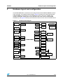
Hardware layout and configuration
Boot option
The STM32100E-EVAL evaluation board is able to boot from:
●
Embedded user Flash
●
System memory with boot loader for ISP
●
Embedded SRAM for debugging
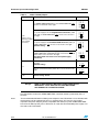
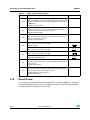
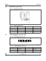
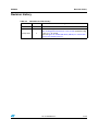
The boot option is configured by setting switch SW1 and SW2.
Table 3.
Boot related switches and jumper
Switch
Switch
configuration
Boot source
STM32100E-EVAL boot from User Flash when BOOT0 is set as shown
to the right:
BOOT1 is don’t care in this configuration.
(Default setting)
STM32100E-EVAL boot from Embedded SRAM when BOOT0 and
BOOT1 are set as shown to the right:
SW1
SW2
STM32100E-EVAL boot from System Memory when BOOT0 and
BOOT1 are set as shown to the right:
The BOOT0 pin of STM32F100ZET6 is connected to RS-232 connector
CN10 pin 6 (DSR) for ISP support when JP8 is closed. This
configuration is used for bootloader application only.
(Default Setting: Not fitted)
JP8
2.4
Clock source
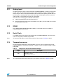
Two clock sources are available on STM32100E-EVAL evaluation board for
STM32F100ZET6 microcontroller:
●
X2, 32 kHz crystal for embedded RTC
●
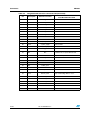
X1, 8 MHz Crystal with socket for STM32F100ZET6 Microcontroller, it can be removed
from its socket when internal RC clock is used.
Table 4.
RTC related solder bridges
Solder bridge
SB5, SB6
Description
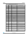
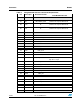
PC14 and PC15 are connected to extension connector CN8 when solder
bridges SB5 and SB6 are closed.
Default Setting: Not fitted
Doc ID 018466 Rev 2
9/48