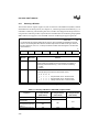
1
8XC196NT
Microcontroller
User’s Manual
8XC196NT
Microcontroller
User’s Manual
June 1995
Information in this document is provided solely to enable use of Intel products. Intel assumes no liability whatsoever, including
infringement of any patent or copyright, for sale and use of Intel products except as provided in Intel’s Terms and Conditions
of Sale for such products.
Intel Corporation makes no warranty for the use of its products and assumes no responsibility for any errors which may appear
in this document nor does it make a commitment to update the information contained herein.
Intel retains the right to make changes to these specifications at any time, without notice.
Contact your local Intel sales office or your distributor to obtain the latest specifications before placing your product order.
MDS is an ordering code only and is not used as a product name or trademark of Intel Corporation.
Intel Corporation and Intel's FASTPATH are not affiliated with Kinetics, a division of Excelan, Inc. or its FASTPATH trademark
or products.
*Other brands and names are the property of their respective owners.
Additional copies of this document or other Intel literature may be obtained from:
Intel Corporation
Literature Sales
P.O. Box 7641
Mt. Prospect, IL 60056-7641
or call 1-800-879-4683
© INTEL CORPORATION, 1996
ii
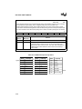
CONTENTS
CHAPTER 1
GUIDE TO THIS MANUAL
1.1
MANUAL CONTENTS ................................................................................................... 1-1
1.2
NOTATIONAL CONVENTIONS AND TERMINOLOGY ................................................ 1-3
1.3
RELATED DOCUMENTS .............................................................................................. 1-5
1.4
ELECTRONIC SUPPORT SYSTEMS ........................................................................... 1-8
1.4.1
FaxBack Service .......................................................................................................1-8
1.4.2
Bulletin Board System (BBS) ....................................................................................1-9
1.4.2.1
How to Find MCS® 96 Microcontroller Files on the BBS ......................................1-9
1.4.2.2
How to Find ApBUILDER Software and Hypertext Documents on the BBS ......1-10
1.4.3
CompuServe Forums ..............................................................................................1-10
1.4.4
World Wide Web .....................................................................................................1-10
1.5
TECHNICAL SUPPORT .............................................................................................. 1-11
1.6
PRODUCT LITERATURE............................................................................................ 1-11
1.7
TRAINING CLASSES .................................................................................................. 1-11
CHAPTER 2
ARCHITECTURAL OVERVIEW
2.1
TYPICAL APPLICATIONS............................................................................................. 2-1
2.2
DEVICE FEATURES ..................................................................................................... 2-1
2.3
BLOCK DIAGRAM ......................................................................................................... 2-1
2.3.1
CPU Control ..............................................................................................................2-3
2.3.2
Register File ..............................................................................................................2-3
2.3.3
Register Arithmetic-logic Unit (RALU) .......................................................................2-3
2.3.3.1
Code Execution ....................................................................................................2-4
2.3.3.2
Instruction Format ................................................................................................2-4
2.3.4
Memory Controller ....................................................................................................2-5
2.3.5
Interrupt Service ........................................................................................................2-5
2.4
INTERNAL TIMING........................................................................................................ 2-6
2.5
INTERNAL PERIPHERALS ........................................................................................... 2-7
2.5.1
I/O Ports ....................................................................................................................2-8
2.5.2
Serial I/O (SIO) Port ..................................................................................................2-8
2.5.3
Synchronous Serial I/O (SSIO) Port ..........................................................................2-8
2.5.4
Slave Port .................................................................................................................2-9
2.5.5
Event Processor Array (EPA) and Timer/Counters ...................................................2-9
2.5.6
Analog-to-digital Converter .....................................................................................2-10
2.5.7
Watchdog Timer ......................................................................................................2-10
2.6
SPECIAL OPERATING MODES ................................................................................. 2-10
2.6.1
Reducing Power Consumption ...............................................................................2-10
2.6.2
Testing the Printed Circuit Board ............................................................................2-11
iii
8XC196NT USER’S MANUAL
2.6.3
Programming the Nonvolatile Memory ....................................................................2-11
CHAPTER 3
PROGRAMMING CONSIDERATIONS
3.1
OVERVIEW OF THE INSTRUCTION SET.................................................................... 3-1
3.1.1
BIT Operands ............................................................................................................3-2
3.1.2
BYTE Operands ........................................................................................................3-2
3.1.3
SHORT-INTEGER Operands ....................................................................................3-2
3.1.4
WORD Operands ......................................................................................................3-3
3.1.5
INTEGER Operands .................................................................................................3-3
3.1.6
DOUBLE-WORD Operands ......................................................................................3-3
3.1.7
LONG-INTEGER Operands ......................................................................................3-4
3.1.8
QUAD-WORD Operands ..........................................................................................3-4
3.1.9
Converting Operands ................................................................................................3-4
3.1.10 Conditional Jumps ....................................................................................................3-4
3.1.11 Floating Point Operations .........................................................................................3-5
3.1.12 Extended Instructions ...............................................................................................3-5
3.2
ADDRESSING MODES ................................................................................................. 3-6
3.2.1
Direct Addressing ......................................................................................................3-7
3.2.2
Immediate Addressing ..............................................................................................3-7
3.2.3
Indirect Addressing ...................................................................................................3-7
3.2.3.1
Extended Indirect Addressing ..............................................................................3-8
3.2.3.2
Indirect Addressing with Autoincrement ...............................................................3-8
3.2.3.3
Extended Indirect Addressing with Autoincrement ...............................................3-8
3.2.3.4
Indirect Addressing with the Stack Pointer ...........................................................3-9
3.2.4
Indexed Addressing ..................................................................................................3-9
3.2.4.1
Short-indexed Addressing ....................................................................................3-9
3.2.4.2
Long-indexed Addressing ....................................................................................3-9
3.2.4.3
Extended Indexed Addressing ...........................................................................3-10
3.2.4.4
Zero-indexed Addressing ...................................................................................3-10
3.2.4.5
Extended Zero-indexed Addressing ...................................................................3-10
3.3
ASSEMBLY LANGUAGE ADDRESSING MODE SELECTIONS ................................ 3-11
3.3.1
Direct Addressing ....................................................................................................3-11
3.3.2
Indexed Addressing ................................................................................................3-11
3.3.3
Extended Addressing ..............................................................................................3-11
3.4
DESIGN CONSIDERATIONS FOR 1-MBYTE DEVICES............................................ 3-11
3.5
SOFTWARE STANDARDS AND CONVENTIONS ..................................................... 3-11
3.5.1
Using Registers .......................................................................................................3-12
3.5.2
Addressing 32-bit Operands ...................................................................................3-12
3.5.3
Addressing 64-bit Operands ...................................................................................3-12
3.5.4
Linking Subroutines ................................................................................................3-13
3.6
SOFTWARE PROTECTION FEATURES AND GUIDELINES .................................... 3-14
iv
CONTENTS
CHAPTER 4
MEMORY PARTITIONS
4.1
MEMORY MAP OVERVIEW.......................................................................................... 4-1
4.2
MEMORY PARTITIONS ................................................................................................ 4-3
4.2.1
External Memory .......................................................................................................4-5
4.2.2
Program and Special-purpose Memory ....................................................................4-5
4.2.2.1
Program Memory in Page FFH ............................................................................4-5
4.2.2.2
Special-purpose Memory .....................................................................................4-6
4.2.2.3
Reserved Memory Locations ...............................................................................4-7
4.2.2.4
Interrupt and PTS Vectors ....................................................................................4-7
4.2.2.5
Security Key .........................................................................................................4-7
4.2.2.6
Chip Configuration Bytes .....................................................................................4-8
4.2.3
Special-function Registers (SFRs) ............................................................................4-8
4.2.3.1
Memory-mapped SFRs ........................................................................................4-8
4.2.3.2
Peripheral SFRs ...................................................................................................4-9
4.2.4
Internal RAM (Code RAM) ......................................................................................4-11
4.2.5
Register File ............................................................................................................4-12
4.2.5.1
General-purpose Register RAM .........................................................................4-13
4.2.5.2
Stack Pointer (SP) ..............................................................................................4-13
4.2.5.3
CPU Special-function Registers (SFRs) .............................................................4-14
4.3
WINDOWING............................................................................................................... 4-15
4.3.1
Selecting a Window ................................................................................................4-16
4.3.2
Addressing a Location Through a Window .............................................................4-17
4.3.2.1
32-byte Windowing Example ..............................................................................4-19
4.3.2.2
64-byte Windowing Example ..............................................................................4-19
4.3.2.3
128-byte Windowing Example ............................................................................4-19
4.3.2.4
Unsupported Locations Windowing Example .....................................................4-20
4.3.2.5
Using the Linker Locator to Set Up a Window ....................................................4-20
4.3.3
Windowing and Addressing Modes .........................................................................4-22
4.4
REMAPPING INTERNAL OTPROM (87C196NT ONLY) ............................................ 4-23
4.5
FETCHING CODE AND DATA IN THE 1-MBYTE AND 64-KBYTE MODES.............. 4-24
4.5.1
Fetching Instructions ...............................................................................................4-24
4.5.2
Accessing Data .......................................................................................................4-24
4.5.2.1
Using Extended Instructions ..............................................................................4-25
4.5.3
Code Fetches in the 1-Mbyte Mode ........................................................................4-26
4.5.4
Code Fetches in the 64-Kbyte Mode ......................................................................4-26
4.5.5
Data Fetches in the 1-Mbyte and 64-Kbyte Modes .................................................4-27
4.6
MEMORY CONFIGURATION EXAMPLES ................................................................. 4-28
4.6.1
Example 1: A 64-Kbyte Mode 87C196NT System ..................................................4-28
4.6.2
Example 2: A 64-Kbyte 87C196NT System with Additional Data Storage ..............4-30
4.6.3
Example 3: A 1-Mbyte 87C196NT System with a 16-bit Bus ..................................4-32
4.6.4
Example 4: A 1-Mbyte 8XC196NT System with an 8-bit Bus .................................4-34
v
8XC196NT USER’S MANUAL
CHAPTER 5
STANDARD AND PTS INTERRUPTS
5.1
OVERVIEW OF INTERRUPTS...................................................................................... 5-1
5.2
INTERRUPT SIGNALS AND REGISTERS ................................................................... 5-3
5.3
INTERRUPT SOURCES AND PRIORITIES.................................................................. 5-4
5.3.1
Special Interrupts ......................................................................................................5-6
5.3.1.1
Unimplemented Opcode ......................................................................................5-6
5.3.1.2
Software Trap .......................................................................................................5-6
5.3.1.3
NMI .......................................................................................................................5-6
5.3.2
External Interrupt Pins ..............................................................................................5-6
5.3.3
Multiplexed Interrupt Sources ...................................................................................5-7
5.3.4
End-of-PTS Interrupts ...............................................................................................5-7
5.4
INTERRUPT LATENCY................................................................................................. 5-7
5.4.1
Situations that Increase Interrupt Latency ................................................................5-8
5.4.2
Calculating Latency ...................................................................................................5-8
5.4.2.1
Standard Interrupt Latency ...................................................................................5-9
5.4.2.2
PTS Interrupt Latency ..........................................................................................5-9
5.5
PROGRAMMING THE INTERRUPTS......................................................................... 5-10
5.5.1
Programming the Multiplexed Interrupts .................................................................5-11
5.5.2
Modifying Interrupt Priorities ...................................................................................5-14
5.5.3
Determining the Source of an Interrupt ...................................................................5-16
5.5.3.1
Determining the Source of Multiplexed Interrupts ..............................................5-16
5.6
INITIALIZING THE PTS CONTROL BLOCKS............................................................. 5-18
5.6.1
Specifying the PTS Count .......................................................................................5-19
5.6.2
Selecting the PTS Mode .........................................................................................5-20
5.6.3
Single Transfer Mode ..............................................................................................5-21
5.6.4
Block Transfer Mode ...............................................................................................5-24
5.6.5
A/D Scan Mode .......................................................................................................5-26
5.6.5.1
A/D Scan Mode Cycles ......................................................................................5-29
5.6.5.2
A/D Scan Mode Example 1 ................................................................................5-29
5.6.5.3
A/D Scan Mode Example 2 ................................................................................5-30
5.6.6
PWM Modes ...........................................................................................................5-31
5.6.6.1
PWM Toggle Mode Example .............................................................................5-33
5.6.6.2
PWM Remap Mode Example .............................................................................5-37
CHAPTER 6
I/O PORTS
6.1
I/O PORTS OVERVIEW ................................................................................................ 6-1
6.2
INPUT-ONLY PORT 0 ................................................................................................... 6-1
6.2.1
Standard Input-only Port Operation ..........................................................................6-2
6.2.2
Standard Input-only Port Considerations ..................................................................6-3
6.3
BIDIRECTIONAL PORTS 1, 2, 5, AND 6 ...................................................................... 6-3
6.3.1
Bidirectional Port Operation ......................................................................................6-5
6.3.2
Bidirectional Port Pin Configurations .........................................................................6-9
vi
CONTENTS
6.3.3
Bidirectional Port Pin Configuration Example .........................................................6-10
6.3.4
Bidirectional Port Considerations ............................................................................6-11
6.3.5
Design Considerations for External Interrupt Inputs ...............................................6-14
6.4
BIDIRECTIONAL PORTS 3 AND 4 (ADDRESS/DATA BUS)...................................... 6-14
6.4.1
Bidirectional Ports 3 and 4 (Address/Data Bus) Operation .....................................6-15
6.4.2
Using Ports 3 and 4 as I/O ......................................................................................6-17
6.4.3
Design Considerations for Ports 3 and 4 ................................................................6-18
6.5
EPORT ........................................................................................................................ 6-18
6.5.1
EPORT Operation ...................................................................................................6-19
6.5.1.1
Reset ..................................................................................................................6-21
6.5.1.2
Output Enable ....................................................................................................6-21
6.5.1.3
Complementary Output Mode ............................................................................6-21
6.5.1.4
Open-drain Output Mode ...................................................................................6-21
6.5.1.5
Input Mode .........................................................................................................6-23
6.5.2
Configuring EPORT Pins ........................................................................................6-24
6.5.2.1
Configuring EPORT Pins for Extended-address Functions ................................6-24
6.5.2.2
Configuring EPORT Pins for I/O ........................................................................6-24
6.5.3
EPORT Considerations ...........................................................................................6-25
6.5.3.1
EPORT Status During Reset, CCB Fetch, Idle, Powerdown, and Hold .............6-25
6.5.3.2
EP_REG Settings for Pins Configured as Extended-address Signals ...............6-25
6.5.3.3
EPORT Status During Instruction Execution ......................................................6-26
6.5.3.4
Design Considerations .......................................................................................6-26
CHAPTER 7
SERIAL I/O (SIO) PORT
7.1
SERIAL I/O (SIO) PORT FUNCTIONAL OVERVIEW ................................................... 7-1
7.2
SERIAL I/O PORT SIGNALS AND REGISTERS .......................................................... 7-2
7.3
SERIAL PORT MODES ................................................................................................. 7-4
7.3.1
Synchronous Mode (Mode 0) ....................................................................................7-4
7.3.2
Asynchronous Modes (Modes 1, 2, and 3) ...............................................................7-5
7.3.2.1
Mode 1 .................................................................................................................7-5
7.3.2.2
Mode 2 .................................................................................................................7-6
7.3.2.3
Mode 3 .................................................................................................................7-7
7.3.2.4
Mode 2 and 3 Timings ..........................................................................................7-7
7.3.2.5
Multiprocessor Communications ..........................................................................7-7
7.4
PROGRAMMING THE SERIAL PORT .......................................................................... 7-8
7.4.1
Configuring the Serial Port Pins ................................................................................7-8
7.4.2
Programming the Control Register ............................................................................7-8
7.4.3
Programming the Baud Rate and Clock Source .......................................................7-8
7.4.4
Enabling the Serial Port Interrupts ..........................................................................7-11
7.4.5
Determining Serial Port Status ................................................................................7-12
7.5
PROGRAMMING EXAMPLE USING AN INTERRUPT-DRIVEN ROUTINE ............... 7-13
vii
8XC196NT USER’S MANUAL
CHAPTER 8
SYNCHRONOUS SERIAL I/O (SSIO) PORT
8.1
SYNCHRONOUS SERIAL I/O (SSIO) PORT FUNCTIONAL OVERVIEW.................... 8-1
8.2
SSIO PORT SIGNALS AND REGISTERS .................................................................... 8-2
8.3
SSIO OPERATION ........................................................................................................ 8-3
8.4
SSIO HANDSHAKING ................................................................................................... 8-6
8.4.1
SSIO Handshaking Configuration .............................................................................8-6
8.4.2
SSIO Handshaking Operation ...................................................................................8-7
8.5
PROGRAMMING THE SSIO PORT .............................................................................. 8-9
8.5.1
Configuring the SSIO Port Pins ................................................................................8-9
8.5.2
Programming the Baud Rate and Enabling the Baud-rate Generator .......................8-9
8.5.3
Controlling the Communications Mode and Handshaking ......................................8-11
8.5.4
Enabling the SSIO Interrupts ..................................................................................8-13
8.5.5
Determining SSIO Port Status ................................................................................8-13
8.6
PROGRAMMING CONSIDERATIONS........................................................................ 8-13
8.7
PROGRAMMING EXAMPLE ....................................................................................... 8-15
CHAPTER 9
SLAVE PORT
9.1
SLAVE PORT FUNCTIONAL OVERVIEW .................................................................... 9-2
9.2
SLAVE PORT SIGNALS AND REGISTERS ................................................................. 9-2
9.3
HARDWARE CONNECTIONS ...................................................................................... 9-6
9.4
SLAVE PORT MODES .................................................................................................. 9-8
9.4.1
Standard Slave Mode Example ................................................................................9-8
9.4.1.1
Master Device Program .......................................................................................9-8
9.4.1.2
Slave Device Program .........................................................................................9-9
9.4.1.3
Demultiplexed Bus Timings ................................................................................9-10
9.4.2
Shared Memory Mode Example ..............................................................................9-11
9.4.2.1
Master Device Program .....................................................................................9-11
9.4.2.2
Slave Device Program .......................................................................................9-12
9.4.2.3
Multiplexed Bus Timings ....................................................................................9-13
9.5
CONFIGURING THE SLAVE PORT............................................................................ 9-14
9.5.1
Programming the Slave Port Control Register (SLP_CON) ....................................9-14
9.5.2
Enabling the Slave Port Interrupts ..........................................................................9-16
9.6
DETERMINING SLAVE PORT STATUS ..................................................................... 9-16
9.7
USING STATUS BITS TO SYNCHRONIZE MASTER AND SLAVE ........................... 9-16
CHAPTER 10
EVENT PROCESSOR ARRAY (EPA)
10.1 EPA FUNCTIONAL OVERVIEW ................................................................................. 10-1
10.2 EPA AND TIMER/COUNTER SIGNALS AND REGISTERS ....................................... 10-2
10.3 TIMER/COUNTER FUNCTIONAL OVERVIEW........................................................... 10-6
10.3.1 Cascade Mode (Timer 2 Only) ................................................................................10-7
viii
CONTENTS
10.3.2 Quadrature Clocking Mode .....................................................................................10-7
10.4 EPA CHANNEL FUNCTIONAL OVERVIEW ............................................................... 10-9
10.4.1 Operating in Capture Mode ...................................................................................10-11
10.4.1.1 Handling EPA Overruns ...................................................................................10-12
10.4.2 Operating in Compare Mode .................................................................................10-13
10.4.2.1 Generating a Low-speed PWM Output ............................................................10-14
10.4.2.2 Generating a Medium-speed PWM Output ......................................................10-15
10.4.2.3 Generating a High-speed PWM Output ...........................................................10-16
10.4.2.4 Generating the Highest-speed PWM Output ....................................................10-16
10.5 PROGRAMMING THE EPA AND TIMER/COUNTERS............................................. 10-17
10.5.1 Configuring the EPA and Timer/Counter Port Pins ...............................................10-17
10.5.2 Programming the Timers .......................................................................................10-17
10.5.3 Programming the Capture/Compare Channels .....................................................10-20
10.5.4 Programming the Compare-only Channels ...........................................................10-25
10.6 ENABLING THE EPA INTERRUPTS ........................................................................ 10-26
10.7 DETERMINING EVENT STATUS.............................................................................. 10-27
10.8 SERVICING THE MULTIPLEXED EPA INTERRUPT WITH SOFTWARE................ 10-29
10.8.1 Using the TIJMP Instruction to Reduce Interrupt Service Overhead ....................10-31
10.9 PROGRAMMING EXAMPLES FOR EPA CHANNELS ............................................. 10-33
10.9.1 EPA Compare Event Program ..............................................................................10-33
10.9.2 EPA Capture Event Program ................................................................................10-34
10.9.3 EPA PWM Output Program ..................................................................................10-35
CHAPTER 11
ANALOG-TO-DIGITAL CONVERTER
11.1 A/D CONVERTER FUNCTIONAL OVERVIEW ........................................................... 11-1
11.2 A/D CONVERTER SIGNALS AND REGISTERS ........................................................ 11-2
11.3 A/D CONVERTER OPERATION ................................................................................. 11-3
11.4 PROGRAMMING THE A/D CONVERTER .................................................................. 11-4
11.4.1 Programming the A/D Test Register .......................................................................11-5
11.4.2 Programming the A/D Result Register (for Threshold Detection Only) ...................11-6
11.4.3 Programming the A/D Time Register ......................................................................11-6
11.4.4 Programming the A/D Command Register ..............................................................11-8
11.4.5 Enabling the A/D Interrupt .......................................................................................11-9
11.5 DETERMINING A/D STATUS AND CONVERSION RESULTS .................................. 11-9
11.6 DESIGN CONSIDERATIONS.................................................................................... 11-10
11.6.1 Designing External Interface Circuitry ...................................................................11-11
11.6.1.1 Minimizing the Effect of High Input Source Resistance ....................................11-12
11.6.1.2 Suggested A/D Input Circuit .............................................................................11-13
11.6.1.3 Analog Ground and Reference Voltages .........................................................11-13
11.6.1.4 Using Mixed Analog and Digital Inputs ............................................................11-14
11.6.2 Understanding A/D Conversion Errors ..................................................................11-14
ix
8XC196NT USER’S MANUAL
CHAPTER 12
MINIMUM HARDWARE CONSIDERATIONS
12.1 MINIMUM CONNECTIONS ......................................................................................... 12-1
12.1.1 Unused Inputs .........................................................................................................12-2
12.1.2 I/O Port Pin Connections ........................................................................................12-2
12.2 APPLYING AND REMOVING POWER ....................................................................... 12-4
12.3 NOISE PROTECTION TIPS ........................................................................................ 12-4
12.4 PROVIDING THE CLOCK ........................................................................................... 12-5
12.4.1 Using the On-chip Oscillator ...................................................................................12-5
12.4.2 Using a Ceramic Resonator Instead of a Crystal Oscillator ....................................12-7
12.4.3 Providing an External Clock Source ........................................................................12-7
12.5 RESETTING THE DEVICE.......................................................................................... 12-8
12.5.1 Generating an External Reset ...............................................................................12-10
12.5.2 Issuing the Reset (RST) Instruction ......................................................................12-12
12.5.3 Issuing an Illegal IDLPD Key Operand .................................................................12-12
12.5.4 Enabling the Watchdog Timer ...............................................................................12-12
12.5.5 Detecting Oscillator Failure ...................................................................................12-12
CHAPTER 13
SPECIAL OPERATING MODES
13.1 SPECIAL OPERATING MODE SIGNALS AND REGISTERS..................................... 13-1
13.2 REDUCING POWER CONSUMPTION ....................................................................... 13-3
13.3 IDLE MODE ................................................................................................................. 13-3
13.4
POWERDOWN MODE ............................................................................................... 13-4
13.4.1 Enabling and Disabling Powerdown Mode ..............................................................13-4
13.4.2 Entering Powerdown Mode .....................................................................................13-5
13.4.3 Exiting Powerdown Mode .......................................................................................13-5
13.4.3.1 Driving the Vpp Pin Low ......................................................................................13-5
13.4.3.2 Generating a Hardware Reset ...........................................................................13-6
13.4.3.3 Asserting the External Interrupt Signal ...............................................................13-6
13.4.3.4 Selecting R1 and C1 ...........................................................................................13-7
13.5 ONCE MODE............................................................................................................... 13-9
13.5.1 Entering and Exiting ONCE Mode ..........................................................................13-9
13.6 RESERVED TEST MODES......................................................................................... 13-9
CHAPTER 14
INTERFACING WITH EXTERNAL MEMORY
14.1 INTERNAL AND EXTERNAL ADDRESSES ............................................................... 14-1
14.2 EXTERNAL MEMORY INTERFACE SIGNALS........................................................... 14-2
14.3 CHIP CONFIGURATION REGISTERS AND CHIP CONFIGURATION BYTES ......... 14-5
14.4 BUS WIDTH AND MULTIPLEXING........................................................................... 14-10
14.4.1 Timing Requirements for BUSWIDTH ...................................................................14-12
14.4.2 16-bit Bus Timings ................................................................................................14-13
x
CONTENTS
14.4.3 8-bit Bus Timings ..................................................................................................14-15
14.5 WAIT STATES (READY CONTROL)......................................................................... 14-17
14.6 BUS-HOLD PROTOCOL ........................................................................................... 14-19
14.6.1 Enabling the Bus-hold Protocol .............................................................................14-21
14.6.2 Disabling the Bus-hold Protocol ............................................................................14-22
14.6.3 Hold Latency .........................................................................................................14-22
14.6.4 Regaining Bus Control ..........................................................................................14-22
14.7 BUS-CONTROL MODES........................................................................................... 14-23
14.7.1 Standard Bus-control Mode ..................................................................................14-23
14.7.2 Write Strobe Mode ................................................................................................14-27
14.7.3 Address Valid Strobe Mode ..................................................................................14-29
14.7.4 Address Valid with Write Strobe Mode ..................................................................14-33
14.8 BUS TIMING MODES................................................................................................ 14-34
14.8.1 Mode 3, Standard Mode .......................................................................................14-36
14.8.2 Mode 0, Standard Timing with One Automatic Wait State ....................................14-36
14.8.3 Mode 1, Long Read/Write Mode ...........................................................................14-36
14.8.4 Mode 2, Long Read/Write with Early Address ......................................................14-37
14.8.5 Design Considerations ..........................................................................................14-39
14.9 SYSTEM BUS AC TIMING SPECIFICATIONS ......................................................... 14-39
CHAPTER 15
PROGRAMMING THE NONVOLATILE MEMORY
15.1 PROGRAMMING METHODS ...................................................................................... 15-1
15.2 OTPROM MEMORY MAP ........................................................................................... 15-2
15.3 SECURITY FEATURES............................................................................................... 15-3
15.3.1 Controlling Access to Internal Memory ...................................................................15-3
15.3.1.1 Controlling Access to the OTPROM During Normal Operation ..........................15-4
15.3.1.2 Controlling Access to the OTPROM During Programming Modes .....................15-4
15.3.2 Controlling Fetches from External Memory .............................................................15-6
15.3.3 Enabling the Oscillator Failure Detection Circuitry ..................................................15-7
15.4 PROGRAMMING PULSE WIDTH ............................................................................... 15-8
15.5 MODIFIED QUICK-PULSE ALGORITHM.................................................................... 15-9
15.6 PROGRAMMING MODE PINS.................................................................................. 15-11
15.7 ENTERING PROGRAMMING MODES ..................................................................... 15-13
15.7.1 Selecting the Programming Mode .........................................................................15-13
15.7.2 Power-up and Power-down Sequences ................................................................15-14
15.7.2.1 Power-up Sequence .........................................................................................15-14
15.7.2.2 Power-down Sequence ....................................................................................15-14
15.8 SLAVE PROGRAMMING MODE............................................................................... 15-15
15.8.1 Reading the Signature Word and Programming Voltages ....................................15-15
15.8.2 Slave Programming Circuit and Memory Map ......................................................15-16
15.8.3 Operating Environment .........................................................................................15-17
15.8.4 Slave Programming Routines ...............................................................................15-19
xi
8XC196NT USER’S MANUAL
15.8.5 Timing Mnemonics ................................................................................................15-24
15.9 AUTO PROGRAMMING MODE ................................................................................ 15-25
15.9.1 Auto Programming Circuit and Memory Map ........................................................15-25
15.9.2 Operating Environment .........................................................................................15-27
15.9.3 Auto Programming Routine ...................................................................................15-27
15.9.4 Auto Programming Procedure ..............................................................................15-29
15.9.5 ROM-dump Mode .................................................................................................15-30
15.10 SERIAL PORT PROGRAMMING MODE .................................................................. 15-31
15.10.1 Serial Port Programming Circuit and Memory Map ...............................................15-31
15.10.2 Changing Serial Port Programming Defaults ........................................................15-33
15.10.3 Executing Programs from Internal RAM ................................................................15-34
15.10.4 Reduced Instruction Set Monitor (RISM) ..............................................................15-34
15.10.5 RISM Command Descriptions ...............................................................................15-35
15.10.6 RISM Command Examples ...................................................................................15-37
15.10.6.1 Example 1 — Programming the PPW ..............................................................15-37
15.10.6.2 Example 2 — Reading OTPROM Contents .....................................................15-38
15.10.6.3 Example 3 — Loading a Program into Internal Code RAM ..............................15-39
15.10.6.4 Example 4 — Setting the PC and Executing the Program ...............................15-41
15.10.6.5 Writing to OTPROM with Examples 3 and 4 ....................................................15-42
15.11 RUN-TIME PROGRAMMING .................................................................................... 15-43
APPENDIX A
INSTRUCTION SET REFERENCE
APPENDIX B
SIGNAL DESCRIPTIONS
B.1
FUNCTIONAL GROUPINGS OF SIGNALS ................................................................. B-1
B.2
SIGNAL DESCRIPTIONS............................................................................................. B-4
B.3
DEFAULT CONDITIONS ............................................................................................ B-14
APPENDIX C
REGISTERS
GLOSSARY
INDEX
xii
CONTENTS
FIGURES
Figure
2-1
2-2
2-3
2-4
4-1
4-2
4-3
4-4
4-5
4-6
4-7
4-8
4-9
4-10
4-11
4-12
5-1
5-2
5-3
5-4
5-5
5-6
5-7
5-8
5-9
5-10
5-11
5-12
5-13
5-14
5-15
5-16
5-17
5-18
5-19
6-1
6-2
6-3
6-4
6-5
7-1
7-2
7-3
7-4
Page
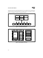
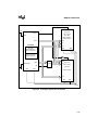
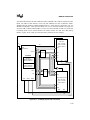
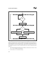
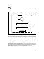
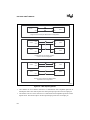
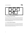
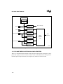
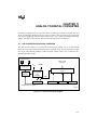
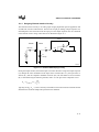
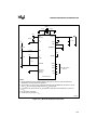
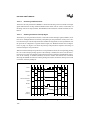
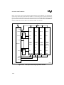
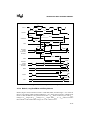
8XC196NT Block Diagram ...........................................................................................2-2
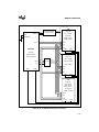
Block Diagram of the Core ...........................................................................................2-2
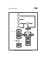
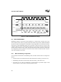
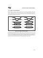
Clock Circuitry ..............................................................................................................2-6
Internal Clock Phases ..................................................................................................2-7
16-Mbyte Address Space .............................................................................................4-2
Pages FFH and 00H.....................................................................................................4-3
Internal RAM Control (IRAM_CON) Register .............................................................4-11
Register File Memory Map .........................................................................................4-12
Windowing ..................................................................................................................4-15
Window Selection Register (WSR).............................................................................4-16
The 24-bit Program Counter.......................................................................................4-24
Formation of Extended and Nonextended Addresses................................................4-25
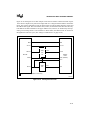
A 64-Kbyte System with an 8-bit Bus .........................................................................4-29
A 64-Kbyte System with Additional Data Storage ......................................................4-31
A 1-Mbyte System with a 16-bit Bus...........................................................................4-33
A 1-Mbyte System with an 8-bit Bus...........................................................................4-35
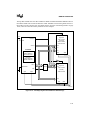
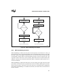
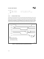
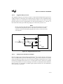
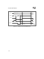
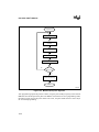
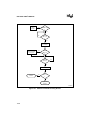
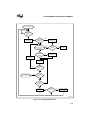
Flow Diagram for PTS and Standard Interrupts ...........................................................5-2
Standard Interrupt Response Time ..............................................................................5-9
PTS Interrupt Response Time ....................................................................................5-10
PTS Select (PTSSEL) Register ..................................................................................5-12
Interrupt Mask (INT_MASK) Register.........................................................................5-13
Interrupt Mask 1 (INT_MASK1) Register....................................................................5-14
Interrupt Pending (INT_PEND) Register ....................................................................5-17
Interrupt Pending 1 (INT_PEND1) Register ...............................................................5-18
PTS Control Blocks ....................................................................................................5-19
PTS Service (PTSSRV) Register ...............................................................................5-20
PTS Mode Selection Bits (PTSCON Bits 7:5) ............................................................5-21
PTS Control Block – Single Transfer Mode................................................................5-22
PTS Control Block – Block Transfer Mode .................................................................5-25
PTS Control Block – A/D Scan Mode .........................................................................5-27
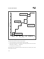
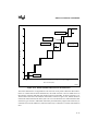
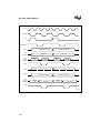
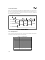
A Generic PWM Waveform ........................................................................................5-32
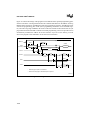
PTS Control Block – PWM Toggle Mode ...................................................................5-34
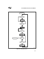
EPA and PTS Operations for the PWM Toggle Mode Example.................................5-36
PTS Control Block – PWM Remap Mode...................................................................5-39
EPA and PTS Operations for the PWM Remap Mode Example ................................5-41
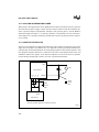
Standard Input-only Port Structure ...............................................................................6-2
Bidirectional Port Structure...........................................................................................6-7
Address/Data Bus (Ports 3 and 4) Structure ..............................................................6-16
EPORT Block Diagram...............................................................................................6-20
EPORT Structure .......................................................................................................6-22
SIO Block Diagram .......................................................................................................7-1
Typical Shift Register Circuit for Mode 0 ......................................................................7-4
Mode 0 Timing..............................................................................................................7-5
Serial Port Frames for Mode 1 .....................................................................................7-6
xiii
8XC196NT USER’S MANUAL
FIGURES
Figure
7-5
7-6
7-7
7-8
8-1
8-2
8-3
8-4
8-5
8-6
8-7
9-1
9-2
9-3
9-4
9-5
9-6
9-7
10-1
10-2
10-3
10-4
10-5
10-6
10-7
10-8
10-9
10-10
10-11
10-12
10-13
10-14
10-15
10-16
11-1
11-2
11-3
11-4
11-5
11-6
11-7
11-8
11-9
11-10
xiv
Page
Serial Port Frames in Mode 2 and 3.............................................................................7-7
Serial Port Control (SP_CON) Register........................................................................7-9
Serial Port Baud Rate (SP_BAUD) Register ..............................................................7-10
Serial Port Status (SP_STATUS) Register.................................................................7-12
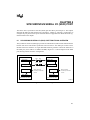
SSIO Block Diagram ....................................................................................................8-1
SSIO Operating Modes ................................................................................................8-4
SSIO Transmit/Receive Timings ..................................................................................8-6
SSIO Handshaking Flow Diagram................................................................................8-7
Synchronous Serial Port Baud (SSIO_BAUD) Register .............................................8-10
Synchronous Serial Control x (SSIOx_CON) Registers .............................................8-11
Variable-width MSB in SSIO Transmissions ..............................................................8-14
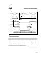
DPRAM vs Slave-port Solution.....................................................................................9-2
Slave Port Block Diagram.............................................................................................9-3
Master/Slave Hardware Connections ...........................................................................9-7
Standard Slave Mode Timings (Demultiplexed Bus) ..................................................9-10
Standard or Shared Memory Mode Timings (Multiplexed Bus)..................................9-13
Slave Port Control (SLP_CON) Register....................................................................9-15
Slave Port Status (SLP_STAT) Register ....................................................................9-17
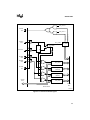
EPA Block Diagram ....................................................................................................10-2
EPA Timer/Counters ..................................................................................................10-6
Quadrature Mode Interface ........................................................................................10-8
Quadrature Mode Timing and Count ..........................................................................10-9
A Single EPA Capture/Compare Channel ................................................................10-10
EPA Simplified Input-capture Structure ....................................................................10-11
Valid EPA Input Events ............................................................................................10-12
Timer 1 Control (T1CONTROL) Register .................................................................10-18
Timer 2 Control (T2CONTROL) Register .................................................................10-19
EPA Control (EPAx_CON) Registers .......................................................................10-21
EPA Compare Control (COMPx_CON) Registers....................................................10-25
EPA Interrupt Mask (EPA_MASK) Register .............................................................10-27
EPA Interrupt Mask 1 (EPA_MASK1) Register ........................................................10-27
EPA Interrupt Pending (EPA_PEND) Register.........................................................10-28
EPA Interrupt Pending 1 (EPA_PEND1) Register....................................................10-28
EPA Interrupt Priority Vector (EPAIPV) Register......................................................10-30
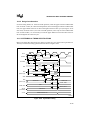
A/D Converter Block Diagram ....................................................................................11-1
A/D Test (AD_TEST) Register....................................................................................11-5
A/D Result (AD_RESULT) Register — Write Format .................................................11-6
A/D Time (AD_TIME) Register ...................................................................................11-7
A/D Command (AD_COMMAND) Register ................................................................11-8
A/D Result (AD_RESULT) Register — Read Format...............................................11-10
Idealized A/D Sampling Circuitry ..............................................................................11-11
Suggested A/D Input Circuit .....................................................................................11-13
Ideal A/D Conversion Characteristic.........................................................................11-16
Actual and Ideal A/D Conversion Characteristics.....................................................11-17
CONTENTS
FIGURES
Figure
11-11
12-1
12-2
12-3
12-4
12-5
12-6
12-7
12-8
12-9
12-10
13-1
13-2
13-3
13-4
14-1
14-2
14-3
14-4
14-5
14-6
14-7
14-8
14-9
14-10
14-11
14-12
14-13
14-14
14-15
14-16
14-17
14-18
14-19
14-20
14-21
14-22
14-23
14-24
14-25
15-1
15-2
15-3
15-4
Page
Terminal-based A/D Conversion Characteristic .......................................................11-19
Minimum Hardware Connections ...............................................................................12-3
Power and Return Connections .................................................................................12-4
On-chip Oscillator Circuit............................................................................................12-6
External Crystal Connections .....................................................................................12-7
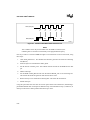
External Clock Connections .......................................................................................12-8
External Clock Drive Waveforms................................................................................12-8
Reset Timing Sequence .............................................................................................12-9
Internal Reset Circuitry .............................................................................................12-10
Minimum Reset Circuit .............................................................................................12-11
Example System Reset Circuit .................................................................................12-11
Clock Control During Power-saving Modes................................................................13-3
Power-up and Powerdown Sequence When Using an External Interrupt ..................13-6
External RC Circuit .....................................................................................................13-7
Typical Voltage on the VPP Pin While Exiting Powerdown.........................................13-8
Chip Configuration 0 (CCR0) Register .......................................................................14-6
Chip Configuration 1 (CCR1) Register .......................................................................14-8
Chip Configuration 2 (CCR2) Register .....................................................................14-10
Multiplexing and Bus Width Options.........................................................................14-11
BUSWIDTH Timing Diagram ....................................................................................14-12
Timings for 16-bit Buses...........................................................................................14-14
Timings for 8-bit Buses.............................................................................................14-16
READY Timing Diagram...........................................................................................14-19
HOLD#, HLDA# Timing ............................................................................................14-20
Standard Bus Control ...............................................................................................14-24
Decoding WRL# and WRH#.....................................................................................14-24
8-bit System with Flash and RAM ............................................................................14-25
16-bit System with Dynamic Bus Width....................................................................14-26
Write Strobe Mode ...................................................................................................14-27
16-bit System with Single-byte Writes to RAM .........................................................14-28
Address Valid Strobe Mode......................................................................................14-29
Comparison of ALE and ADV# Bus Cycles ..............................................................14-30
8-bit System with Flash ............................................................................................14-31
16-bit System with Flash ..........................................................................................14-32
Timings of Address Valid with Write Strobe Mode ...................................................14-33
16-bit System with RAM ...........................................................................................14-34
Modes 0, 1, 2, and 3 Timings ...................................................................................14-35
Mode 1 System Bus Timing......................................................................................14-37
Mode 2 System Bus Timing......................................................................................14-38
System Bus Timing ..................................................................................................14-39
Unerasable PROM (USFR) Register..........................................................................15-7
Programming Pulse Width (PPW or SP_PPW) Register............................................15-9
Modified Quick-pulse Algorithm................................................................................15-10
Pin Functions in Programming Modes......................................................................15-11
xv
8XC196NT USER’S MANUAL
FIGURES
Figure
15-5
15-6
15-7
15-8
15-9
15-10
15-11
15-12
15-13
15-14
15-15
B-1
xvi
Page
Slave Programming Circuit.......................................................................................15-16
Chip Configuration Registers (CCRs).......................................................................15-18
Address/Command Decoding Routine .....................................................................15-20
Program Word Routine.............................................................................................15-21
Program Word Waveform.........................................................................................15-22
Dump Word Routine .................................................................................................15-23
Dump Word Waveform .............................................................................................15-24
Auto Programming Circuit ........................................................................................15-26
Auto Programming Routine ......................................................................................15-28
Serial Port Programming Mode Circuit .....................................................................15-32
Run-time Programming Code Example....................................................................15-44
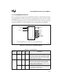
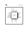
8XC196NT 68-lead PLCC Package ............................................................................ B-3
CONTENTS
TABLES
Table
1-1
1-2
1-3
1-4
1-5
2-1
2-2
3-1
3-2
3-3
4-1
4-2
4-3
4-4
4-5
4-6
4-7
4-8
4-9
4-10
4-11
4-12
4-13
4-14
4-15
4-16
4-17
5-1
5-2
5-3
5-4
5-5
5-6
5-7
5-8
5-9
5-10
5-11
5-12
5-13
5-14
6-1
6-2
6-3
Page
Handbooks and Product Information ............................................................................1-6
Application Notes, Application Briefs, and Article Reprints ..........................................1-6
MCS® 96 Microcontroller Datasheets (Commercial/Express) ......................................1-7
MCS® 96 Microcontroller Datasheets (Automotive) .....................................................1-7
MCS® 96 Microcontroller Quick References ................................................................1-7
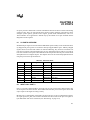
Features of the 8XC196NT ..........................................................................................2-1
State Times at Various Frequencies ............................................................................2-7
Operand Type Definitions.............................................................................................3-1
Equivalent Operand Types for Assembly and C Programming Languages .................3-2
Definition of Temporary Registers ................................................................................3-7
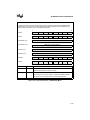
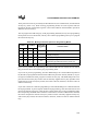
8XC196NT Memory Map..............................................................................................4-4
Program Memory Access for the 87C196NT................................................................4-6
Special-purpose Memory Access for the 87C196NT ...................................................4-6
8XC196NT Special-purpose Memory Addresses.........................................................4-7
8XC196NT Memory-mapped SFRs..............................................................................4-9
8XC196NT Peripheral SFRs ......................................................................................4-10
Register File Memory Addresses ...............................................................................4-13
8XC196NT CPU SFRs ...............................................................................................4-14
Selecting a Window of 8XC196NT Peripheral SFRs..................................................4-16
Selecting a Window of the Upper Register File ..........................................................4-17
Windows .....................................................................................................................4-18
Windowed Base Addresses .......................................................................................4-19
Memory Access for the 87C196NT ............................................................................4-23
Memory Map for the System in Figure 4-9 .................................................................4-30
Memory Map for the System in Figure 4-10 ...............................................................4-32
Memory Map for the System in Figure 4-11 ...............................................................4-34
Memory Map for the System in Figure 4-12 ...............................................................4-36
Interrupt Signals ...........................................................................................................5-3
Interrupt and PTS Control and Status Registers ..........................................................5-3
Interrupt Sources, Vectors, and Priorities.....................................................................5-5
Execution Times for PTS Cycles ................................................................................5-10
Single Transfer Mode PTSCB ....................................................................................5-24
Block Transfer Mode PTSCB .....................................................................................5-24
A/D Scan Mode Command/Data Table ......................................................................5-28
Command/Data Table (Example 1) ............................................................................5-30
A/D Scan Mode PTSCB (Example 1) .........................................................................5-30
Command/Data Table (Example 2) ............................................................................5-30
A/D Scan Mode PTSCB (Example 2) .........................................................................5-31
Comparison of PWM Modes.......................................................................................5-32
PWM Toggle Mode PTSCB........................................................................................5-33
PWM Remap Mode PTSCB .......................................................................................5-38
Device I/O Ports ...........................................................................................................6-1
Standard Input-only Port Pins ......................................................................................6-2
Input-only Port Registers ..............................................................................................6-2
xvii
8XC196NT USER’S MANUAL
TABLES
Table
6-4
6-5
6-6
6-7
6-8
6-9
6-10
6-11
6-12
6-13
6-14
6-15
6-16
6-17
6-18
6-19
7-1
7-2
7-3
8-1
8-2
8-3
9-1
9-2
9-3
10-1
10-2
10-3
10-4
10-5
10-6
11-1
11-2
12-1
12-2
13-1
13-2
14-1
14-2
14-3
14-4
14-5
14-6
14-7
xviii
Page
Bidirectional Port Pins ..................................................................................................6-4
Bidirectional Port Control and Status Registers ...........................................................6-5
Logic Table for Bidirectional Ports in I/O Mode ............................................................6-8
Logic Table for Bidirectional Ports in Special-function Mode .......................................6-8
Control Register Values for Each Configuration.........................................................6-10
Port Configuration Example .......................................................................................6-10
Port Pin States After Reset and After Example Code Execution................................6-11
Ports 3 and 4 Pins ......................................................................................................6-15
Ports 3 and 4 Control and Status Registers ...............................................................6-15
Logic Table for Ports 3 and 4 as I/O...........................................................................6-17
EPORT Pins ...............................................................................................................6-18
EPORT Control and Status Registers ........................................................................6-18
Logic Table for EPORT in I/O Mode...........................................................................6-23
Logic Table for EPORT in Address Mode ..................................................................6-23
Configuration Register Settings for EPORT Pins .......................................................6-24
EPORT Pin Status During Reset, CCB Fetch, Idle, Powerdown, and Hold ...............6-25
Serial Port Signals ........................................................................................................7-2
Serial Port Control and Status Registers......................................................................7-2
SP_BAUD Values When Using XTAL1 at 20 MHz.....................................................7-11
SSIO Port Signals ........................................................................................................8-2
SSIO Port Control and Status Registers ......................................................................8-2
Common SSIO_BAUD Values When Using XTAL1 at 20 MHz .................................8-10
Slave Port Signals ........................................................................................................9-4
Slave Port Control and Status Registers ......................................................................9-4
Master and Slave Interconnections ..............................................................................9-6
EPA and Timer/Counter Signals.................................................................................10-3
EPA Control and Status Registers .............................................................................10-3
Quadrature Mode Truth Table ....................................................................................10-8
Action Taken when a Valid Edge Occurs .................................................................10-12
Example Control Register Settings and EPA Operations.........................................10-20
EPAIPV Interrupt Priority Values ..............................................................................10-30
A/D Converter Pins.....................................................................................................11-2
A/D Control and Status Registers...............................................................................11-2
Minimum Required Signals.........................................................................................12-1
I/O Port Configuration Guide ......................................................................................12-2
Operating Mode Control Signals ................................................................................13-1
Operating Mode Control and Status Registers...........................................................13-2
Example of Internal and External Addresses .............................................................14-1
External Memory Interface Signals.............................................................................14-2
READY Signal Timing Definitions.............................................................................14-18
HOLD#, HLDA# Timing Definitions ..........................................................................14-20
Maximum Hold Latency ............................................................................................14-22
Bus-control Mode .....................................................................................................14-23
Modes 0, 1, 2, and 3 Timing Comparisons...............................................................14-36
CONTENTS
TABLES
Table
14-8
14-9
15-1
15-2
15-3
15-4
15-5
15-6
15-7
15-8
15-9
15-10
15-11
15-12
15-13
15-14
A-1
A-1
A-2
A-3
A-4
A-5
A-6
A-7
A-8
A-9
B-1
B-2
B-3
B-4
B-5
B-6
C-1
C-2
C-3
C-4
C-5
C-6
C-7
C-8
C-9
C-10
C-11
C-12
Page
AC Timing Symbol Definitions ..................................................................................14-40
AC Timing Definitions ...............................................................................................14-40
87C196NT OTPROM Memory Map ...........................................................................15-2
Memory Protection for Normal Operating Mode.........................................................15-4
Memory Protection Options for Programming Modes ................................................15-5
UPROM Programming Values and Locations for Slave Mode ...................................15-8
Pin Descriptions .......................................................................................................15-11
PMODE Values ........................................................................................................15-13
Device Signature Word and Programming Voltages ................................................15-16
Slave Programming Mode Memory Map ..................................................................15-17
Timing Mnemonics ...................................................................................................15-24
Auto Programming Memory Map..............................................................................15-27
87C196NT Serial Port Programming Mode Memory Map........................................15-33
87C196NT Serial Port Programming Default Values and Locations ........................15-33
User Program Register Values and Test ROM Locations ........................................15-34
RISM Command Descriptions ..................................................................................15-35
Opcode Map (Left Half) ............................................................................................... A-2
Opcode Map (Right Half)............................................................................................. A-3
Processor Status Word (PSW) Flags .......................................................................... A-4
Effect of PSW Flags or Specified Bits on Conditional Jump Instructions .................... A-5
PSW Flag Setting Symbols ......................................................................................... A-5
Operand Variables ...................................................................................................... A-6
Instruction Set ............................................................................................................. A-7
Instruction Opcodes .................................................................................................. A-46
Instruction Lengths and Hexadecimal Opcodes ........................................................ A-52
Instruction Execution Times (in State Times) ............................................................ A-59
Signal Name Changes ................................................................................................ B-1
8XC196NT Signals Arranged by Functional Categories ............................................. B-2
Description of Columns of Table B-4........................................................................... B-4
Signal Descriptions...................................................................................................... B-4
Definition of Status Symbols ..................................................................................... B-14
8XC196NT Pin Status ............................................................................................... B-14
Modules and Related Registers .................................................................................. C-1
Register Name, Address, and Reset Status................................................................ C-2
COMPx_CON Addresses and Reset Values............................................................. C-15
COMPx_TIME Addresses and Reset Values ............................................................ C-16
EPAx_CON Addresses and Reset Values ................................................................ C-28
EPAx_TIME Addresses and Reset Values................................................................ C-29
EPA Interrupt Priority Vectors.................................................................................... C-30
Px_DIR Addresses and Reset Values....................................................................... C-37
Px_MODE Addresses and Reset Values .................................................................. C-38
Special-function Signals for Ports 1, 2, 5, 6............................................................... C-39
Px_PIN Addresses and Reset Values ....................................................................... C-40
Px_REG Addresses and Reset Values ..................................................................... C-41
xix
8XC196NT USER’S MANUAL
TABLES
Table
C-13
C-14
C-15
C-16
C-17
xx
Page
Common SSIO_BAUD Values When Using XTAL1 at 20 MHz ................................ C-57
SSIOx_BUF Addresses and Reset Values................................................................ C-58
SSIOx_CON Addresses and Reset Values............................................................... C-60
TIMERx Addresses and Reset Values ...................................................................... C-63
WSR Settings and Direct Addresses for Windowable SFRs ..................................... C-66
1
Guide to This Manual
CHAPTER 1
GUIDE TO THIS MANUAL
This manual describes the 8XC196NT embedded microcontroller. It is intended for use by both
software and hardware designers familiar with the principles of microcontrollers. This chapter
describes what you’ll find in this manual, lists other documents that may be useful, and explains
how to access the support services we provide to help you complete your design.
1.1
MANUAL CONTENTS
This manual contains several chapters and appendixes, a glossary, and an index. This chapter,
Chapter 1, provides an overview of the manual. This section summarizes the contents of the remaining chapters and appendixes. The remainder of this chapter describes notational conventions
and terminology used throughout the manual, provides references to related documentation, describes customer support services, and explains how to access information and assistance.
Chapter 2 — Architectural Overview — provides an overview of the device hardware. It describes the core, internal timing, internal peripherals, and special operating modes.
Chapter 3 — Programming Considerations — provides an overview of the instruction set, describes general standards and conventions, and defines the operand types and addressing modes
supported by the MCS® 96 microcontroller family. (For additional information about the instruction set, see Appendix A.)
Chapter 4 — Memory Partitions — describes the addressable memory space of the device. It
describes the memory partitions, explains how to use windows to increase the amount of memory
that can be accessed with register-direct (8-bit) instructions, and provides examples of memory
configurations.
Chapter 5 — Standard and PTS Interrupts — describes the interrupt control circuitry, priority
scheme, and timing for standard and peripheral transaction server (PTS) interrupts. It also explains interrupt programming and control.
Chapter 6 — I/O Ports — describes the input/output ports and explains how to configure the
ports for input, output, or special functions.
Chapter 7 — Serial I/O (SIO) Port — describes the asynchronous/synchronous serial I/O (SIO)
port and explains how to program it.
1-1
8XC196NT USER’S MANUAL
Chapter 8 — Synchronous Serial I/O (SSIO) Port — describes the synchronous serial I/O
(SSIO) port and explains how to program it.
Chapter 9 — Slave Port — describes the slave port and explains how to program it. Chapter 6,
“I/O Ports,” explains how to configure port 3 to serve as the slave port. This chapter discusses
additional configurations specific to the slave port function and describes how to use the slave
port for interprocessor communication.
Chapter 10 — Event Processor Array (EPA) — describes the event processor array, a timer/counter-based, high-speed input/output unit. It describes the timer/counters and explains how
to program the EPA and how to use the EPA to produce pulse-width modulated (PWM) outputs.
Chapter 11 — Analog-to-digital Converter — provides an overview of the analog-to-digital
(A/D) converter and describes how to program the converter, read the conversion results, and interface with external circuitry.
Chapter 12 — Minimum Hardware Considerations — describes options for providing the basic requirements for device operation within a system, discusses other hardware considerations,
and describes device reset options.
Chapter 13 — Special Operating Modes — provides an overview of the idle, powerdown, and
on-circuit emulation (ONCE) modes and describes how to enter and exit each mode.
Chapter 14 — Interfacing with External Memory — lists the external memory signals and describes the registers that control the external memory interface. It discusses the bus width and
memory configurations, the bus-hold protocol, write-control modes, and internal wait states and
ready control. Finally, it provides timing information for the system bus.
Chapter 15 — Programming the Nonvolatile Memory — provides recommended circuits, the
corresponding memory maps, and flow diagrams. It also provides procedures for auto programming, and describes the commands used for serial port programming.
Appendix A — Instruction Set Reference — provides reference information for the instruction
set. It describes each instruction; defines the processor status word (PSW) flags; shows the relationships between instructions and PSW flags; and lists hexadecimal opcodes, instruction
lengths, and execution times. (For additional information about the instruction set, see Chapter 3,
“Programming Considerations.”)
Appendix B — Signal Descriptions — provides reference information for the device pins, including descriptions of the pin functions, reset status of the I/O and control pins, and package pin
assignments.
1-2
GUIDE TO THIS MANUAL
Appendix C — Registers — provides a compilation of all device registers arranged alphabetically by register mnemonic. It also includes tables that list the windowed direct addresses for all
SFRs in each possible window.
Glossary — defines terms with special meaning used throughout this manual.
Index — lists key topics with page number references.
1.2
NOTATIONAL CONVENTIONS AND TERMINOLOGY
The following notations and terminology are used throughout this manual. The Glossary defines
other terms with special meanings.
#
The pound symbol (#) has either of two meanings, depending on the
context. When used with a signal name, the symbol means that the
signal is active low. When used in an instruction, the symbol prefixes
an immediate value in immediate addressing mode.
Addresses
In this manual, both internal and external addresses use the number
of hexadecimal digits that correspond with the number of available
address lines. For example, the highest possible internal address is
shown as FFFFFFH, while the highest possible external address is
shown as FFFFFH. When writing code, use the appropriate address
conventions for the software tool you are using. (For assembly code,
a zero must precede an alphabetic character and an “H” must follow
a hexadecimal value, so FFFFFFH must be written as 0FFFFFFH.
For ‘C’ code, a zero plus an “x” must precede a hexadecimal value,
so FFFFFFH must be written as 0xFFFFFF.)
Assert and Deassert
The terms assert and deassert refer to the act of making a signal
active (enabled) and inactive (disabled), respectively. The active
polarity (low or high) is defined by the signal name. Active-low
signals are designated by a pound symbol (#) suffix; active-high
signals have no suffix. To assert RD# is to drive it low; to assert ALE
is to drive it high; to deassert RD# is to drive it high; to deassert ALE
is to drive it low.
Clear and Set
The terms clear and set refer to the value of a bit or the act of giving
it a value. If a bit is clear, its value is “0”; clearing a bit gives it a “0”
value. If a bit is set, its value is “1”; setting a bit gives it a “1” value.
Instructions
Instruction mnemonics are shown in upper case to avoid confusion.
You may use either upper case or lower case.
1-3
8XC196NT USER’S MANUAL
italics
Italics identify variables and introduce new terminology. The context
in which italics are used distinguishes between the two possible
meanings.
Variables in registers and signal names are commonly represented by
x and y, where x represents the first variable and y represents the
second variable. For example, in register Px_MODE.y, x represents
the variable that identifies the specific port, and y represents the
register bit variable (7:0 or 15:0). Variables must be replaced with the
correct values when configuring or programming registers or
identifying signals.
Numbers
Hexadecimal numbers are represented by a string of hexadecimal
digits followed by the character H. Decimal and binary numbers are
represented by their customary notations. (That is, 255 is a decimal
number and 1111 1111 is a binary number. In some cases, the letter B
is appended to binary numbers for clarity.)
Register Bits
Bit locations are indexed by 7:0 (or 15:0), where bit 0 is the leastsignificant bit and bit 7 (or 15) is the most-significant bit. An
individual bit is represented by the register name, followed by a
period and the bit number. For example, WSR.7 is bit 7 of the
window selection register. In some discussions, bit names are used.
Register Names
Register mnemonics are shown in upper case. For example, TIMER2
is the timer 2 register; timer 2 is the timer. A register name containing
a lowercase italic character represents more than one register. For
example, the x in Px_REG indicates that the register name refers to
any of the port data registers.
Reserved Bits
Certain bits are described as reserved bits. In illustrations, reserved
bits are indicated with a dash (—). These bits are not used in this
device, but they may be used in future implementations. To help
ensure that a current software design is compatible with future implementations, reserved bits should be cleared (given a value of “0”) or
left in their default states, unless otherwise noted.
Signal Names
Signal names are shown in upper case. When several signals share a
common name, an individual signal is represented by the signal name
followed by a number. For example, the EPA signals are named
EPA0, EPA1, EPA2, etc. Port pins are represented by the port abbreviation, a period, and the pin number (e.g., P1.0, P1.1). A pound
symbol (#) appended to a signal name identifies an active-low signal.
1-4
GUIDE TO THIS MANUAL
Units of Measure
The following abbreviations are used to represent units of measure:
A
DCV
Kbytes
kHz
kΩ
mA
Mbytes
MHz
ms
mW
ns
pF
W
V
µA
µF
µs
µW
X
1.3
amps, amperes
direct current volts
kilobytes
kilohertz
kilo-ohms
milliamps, milliamperes
megabytes
megahertz
milliseconds
milliwatts
nanoseconds
picofarads
watts
volts
microamps, microamperes
microfarads
microseconds
microwatts
Uppercase X (no italics) represents an unknown value or an
immaterial (“don’t care”) state or condition. The value may be either
binary or hexadecimal, depending on the context. For example,
2XAFH (hex) indicates that bits 11:8 are unknown; 10XXB(binary)
indicates that the two LSBs are unknown.
RELATED DOCUMENTS
The tables in this section list additional documents that you may find useful in designing systems
incorporating MCS 96 microcontrollers. These are not comprehensive lists, but are a representative sample of relevant documents. For a complete list of available printed documents, please order the literature catalog (order number 210621). To order documents, please call the Intel
literature center for your area (telephone numbers are listed on page 1-11).
Intel’s ApBUILDER software, hypertext manuals and datasheets, and electronic versions of application notes and code examples are also available from the BBS (see “Bulletin Board System
(BBS)” on page 1-9). New information is available first from FaxBack and the BBS. Refer to
“Electronic Support Systems” on page 1-8 for details.
1-5
8XC196NT USER’S MANUAL
Table 1-1. Handbooks and Product Information
Title and Description
Order Number
Intel Embedded Quick Reference Guide
Solutions for Embedded Applications Guide
Data on Demand fact sheet
Data on Demand annual subscription (6 issues; Windows* version)
Complete set of Intel handbooks on CD-ROM.
Handbook Set — handbooks and product overview
Complete set of Intel’s product line handbooks. Contains datasheets, application
notes, article reprints and other design information on microprocessors, peripherals, embedded controllers, memory components, single-board computers,
microcommunications, software development tools, and operating systems.
Automotive Products †
Application notes and article reprints on topics including the MCS 51 and MCS 96
microcontrollers. Documents in this handbook discuss hardware and software
implementations and present helpful design techniques.
Embedded Applications handbook (2 volume set) †
Data sheets, architecture descriptions, and application ntoes on topics including
flash memory devices, networking chips, and MCS 51 and MCS 96 microcontrollers. Documents in this handbook discuss hardware and software implementations and present helpful design techniques.
Embedded Microcontrollers †
Data sheets and architecture descriptions for Intel’s three industry-standard
microcontrollers, the MCS ® 48, MCS 51, and MCS 96 microcontrollers.
Peripheral Components †
Comprehensive information on Intel’s peripheral components, including
datasheets, application notes, and technical briefs.
Flash Memory (2 volume set) †
A collection of data sheets and application notes devoted to techniques and
information to help design semiconductor memory into an application or system.
Packaging †
Detailed information on the manufacturing, applications, and attributes of a variety
of semiconductor packages.
Development Tools Handbook
Information on third-party hardware and software tools that support Intel’s
embedded microcontrollers.
† Included in handbook set (order number 231003)
272439
240691
240952
240897
231003
231792
270648
270646
296467
210830
240800
272326
Table 1-2. Application Notes, Application Briefs, and Article Reprints
Title
Order Number
AB-71, Using the SIO on the 8XC196MH (application brief)
272594
AP-125, Design Microcontroller Systems for Electrically Noisy Environments †††
210313
AP-155, Oscillators for Microcontrollers †††
230659
AR-375, Motor Controllers Take the Single-Chip Route (article reprint)
270056
AP-406, MCS® 96 Analog Acquisition Primer †††
270365
AP-445, 8XC196KR Peripherals: A User’s Point of View
†
† Included in Automotive Products handbook (order number 231792)
†† Included in Embedded Applications handbook (order number 270648)
††† Included in Automotive Products and Embedded Applications handbooks
1-6
270873
GUIDE TO THIS MANUAL
Table 1-2. Application Notes, Application Briefs, and Article Reprints (Continued)
Title
Order Number
AP-449, A Comparison of the Event Processor Array (EPA) and High Speed
Input/Output (HSIO) Unit †
270968
AP-475, Using the 8XC196NT ††
272315
AP-477, Low Voltage Embedded Design ††
272324
AP-483, Application Examples Using the 8XC196MC/MD Microcontroller
272282
AP-700, Intel Fuzzy Logic Tool Simplifies ABS Design †
272595
AP-711, EMI Design Techniques for Microcontrollers in Automotive Applications
272324
AP-715, Interfacing an I2C Serial EEPROM to an MCS® 96 Microcontroller
272680
† Included in Automotive Products handbook (order number 231792)
†† Included in Embedded Applications handbook (order number 270648)
††† Included in Automotive Products and Embedded Applications handbooks
Table 1-3. MCS® 96 Microcontroller Datasheets (Commercial/Express)
Title
Order Number
†
8XC196KR/KQ/JR/JQ Commercial/Express CHMOS Microcontroller
8XC196KT Commercial CHMOS Microcontroller †
87C196KT/87C196KS 20 MHz Advanced 16-Bit CHMOS Microcontroller †
8XC196MC Industrial Motor Control Microcontroller †
87C196MD Industrial Motor Control CHMOS Microcontroller †
8XC196NP Commercial CHMOS 16-Bit Microcontroller †
8XC196NT CHMOS Microcontroller with 1-Mbyte Linear Address Space †
† Included in Embedded Microcontrollers handbook (order number 270646)
270912
272266
272513
272323
270946
272459
272267
Table 1-4. MCS® 96 Microcontroller Datasheets (Automotive)
Title and Description
87C196CA/87C196CB 20 MHz Advanced 16-Bit CHMOS Microcontroller with
Integrated CAN 2.0 †
87C196JT 20 MHz Advanced 16-Bit CHMOS Microcontroller †
87C196JV 20 MHz Advanced 16-Bit CHMOS Microcontroller †
87C196KR/KQ, 87C196JV/JT, 87C196JR/JQ Advanced 16-Bit CHMOS
Microcontroller †
87C196KT/87C196KS Advanced 16-Bit CHMOS Microcontroller †
87C196KT/KS 20 MHz Advanced 16-Bit CHMOS Microcontroller †
† Included in Automotive Products handbook (order number 231792)
Order Number
272405
272529
272580
270827
270999
272513
Table 1-5. MCS® 96 Microcontroller Quick References
Title and Description
8XC196KR Quick Reference (includes the JQ, JR, KQ, KR)
8XC196KT Quick Reference
8XC196MC Quick Reference
8XC196NP Quick Reference
8XC196NT Quick Reference
Order Number
272113
272269
272114
272466
272270
1-7
8XC196NT USER’S MANUAL
1.4
ELECTRONIC SUPPORT SYSTEMS
Intel’s FaxBack* service and application BBS provide up-to-date technical information. We also
maintain several forums on CompuServe and offer a variety of information on the World Wide
Web. These systems are available 24 hours a day, 7 days a week, providing technical information
whenever you need it.
1.4.1
FaxBack Service
FaxBack is an on-demand publishing system that sends documents to your fax machine. You can
get product announcements, change notifications, product literature, device characteristics, design recommendations, and quality and reliability information from FaxBack 24 hours a day, 7
days a week.
1-800-628-2283
U.S. and Canada
916-356-3105
U.S., Canada, Japan, APac
44(0)1793-496646
Europe
Think of the FaxBack service as a library of technical documents that you can access with your
phone. Just dial the telephone number and respond to the system prompts. After you select a document, the system sends a copy to your fax machine.
Each document is assigned an order number and is listed in a subject catalog. The first time you
use FaxBack, you should order the appropriate subject catalogs to get a complete listing of document order numbers. Catalogs are updated twice monthly, so call for the latest information. The
following catalogs and information are available at the time of publication:
1.
Solutions OEM subscription form
2.
Microcontroller and flash catalog
3.
Development tools catalog
4.
Systems catalog
5.
Multimedia catalog
6.
Multibus and iRMX ® software catalog and BBS file listings
7.
Microprocessor, PCI, and peripheral catalog
8.
Quality and reliability and change notification catalog
9.
iAL (Intel Architecture Labs) technology catalog
1-8
GUIDE TO THIS MANUAL
1.4.2
Bulletin Board System (BBS)
The bulletin board system (BBS) lets you download files to your computer. The application BBS
has the latest ApBUILDER software, hypertext manuals and datasheets, software drivers, firmware upgrades, application notes and utilities, and quality and reliability data.
916-356-3600
U.S., Canada, Japan, APac (up to 19.2 Kbaud)
916-356-7209
U.S., Canada, Japan, APac (2400 baud only)
44(0)1793-496340
Europe
The toll-free BBS (available in the U.S. and Canada) offers lists of documents available from
FaxBack, a master list of files available from the application BBS, and a BBS user’s guide. The
BBS file listing is also available from FaxBack (catalog number 6; see page 1-8 for phone numbers and a description of the FaxBack service).
1-800-897-2536
U.S. and Canada only
Any customer with a modem and computer can access the BBS. The system provides automatic
configuration support for 1200- through 19200-baud modems. Typical modem settings are 14400
baud, no parity, 8 data bits, and 1 stop bit (14400, N, 8, 1).
To access the BBS, just dial the telephone number and respond to the system prompts. During
your first session, the system asks you to register with the system operator by entering your name
and location. The system operator will set up your access account within 24 hours. At that time,
you can access the files on the BBS.
NOTE
If you encounter any difficulty accessing the high-speed modem, try the
dedicated 2400-baud modem. Use these modem settings: 2400, N, 8, 1.
1.4.2.1
How to Find MCS® 96 Microcontroller Files on the BBS
Application notes, utilities, and product literature are available from the BBS. To access the files,
complete these steps:
1.
Enter F from the BBS Main menu. The BBS displays the Intel Apps Files menu.
2.
Type L and press <Enter>. The BBS displays the list of areas and prompts for the area
number.
3.
Type 12 and press <Enter> to select MCS 96 Family. The BBS displays a list of subject
areas including general and product-specific subjects.
4.
Type the number that corresponds to the subject of interest and press <Enter> to list the
latest files.
1-9
8XC196NT USER’S MANUAL
5.
Type the file numbers to select the files you wish to download (for example, 1,6 for files 1
and 6 or 3-7 for files 3, 4, 5, 6, and 7) and press <Enter>. The BBS displays the approximate time required to download the files you have selected and gives you the option to
download them.
1.4.2.2
How to Find ApBUILDER Software and Hypertext Documents on the BBS
The latest ApBUILDER files and hypertext manuals and data sheets are available first from the
BBS. To access the files, complete these steps:
1.
Type F from the BBS Main menu. The BBS displays the Intel Apps Files menu.
2.
Type L and press <Enter>. The BBS displays the list of areas and prompts for the area
number.
3.
Type 25 and press <Enter> to select ApBUILDER/Hypertext. The BBS displays several
options: one for ApBUILDER software and the others for hypertext documents for
specific product families.
4.
Type 1 and press <Enter> to list the latest ApBUILDER files or type 2 and press <Enter>
to list the hypertext manuals and datasheets for MCS 96 microcontrollers.
5.
Type the file numbers to select the files you wish to download (for example, 1,6 for files 1
and 6 or 3-7 for files 3, 4, 5, 6, and 7) and press <Enter>. The BBS displays the approximate time required to download the selected files and gives you the option to download
them.
1.4.3
CompuServe Forums
The CompuServe forums provide a means for you to gather information, share discoveries, and
debate issues. Type “go intel” for access. For information about CompuServe access and service
fees, call CompuServe at 1-800-848-8199 (U.S.) or 614-529-1340 (outside the U.S.).
1.4.4
World Wide Web
We offer a variety of information through the World Wide Web (URL:http://www.intel.com/). Select “Embedded Design Products” from the Intel home page.
1-10
GUIDE TO THIS MANUAL
1.5
TECHNICAL SUPPORT
In the U.S. and Canada, technical support representatives are available to answer your questions
between 5 a.m. and 5 p.m. PST. You can also fax your questions to us. (Please include your voice
telephone number and indicate whether you prefer a response by phone or by fax). Outside the
U.S. and Canada, please contact your local distributor.
1-800-628-8686
U.S. and Canada
916-356-7599
U.S. and Canada
916-356-6100 (fax)
U.S. and Canada
1.6
PRODUCT LITERATURE
You can order product literature from the following Intel literature centers.
1-800-468-8118, ext. 283
U.S. and Canada
708-296-9333
U.S. (from overseas)
44(0)1793-431155
Europe (U.K.)
44(0)1793-421333
Germany
44(0)1793-421777
France
81(0)120-47-88-32
Japan (fax only)
1.7
TRAINING CLASSES
In the U.S. and Canada, you can register for training classes through the Intel customer training
center. Classes are held in the U.S.
1-800-234-8806
U.S. and Canada
1-11
2
Architectural
Overview
CHAPTER 2
ARCHITECTURAL OVERVIEW
The 16-bit 8XC196NT CHMOS microcontroller is designed to handle high-speed calculations
and fast input/output (I/O) operations. It shares a common architecture and instruction set with
other members of the MCS® 96 microcontroller family. This device extends the addressability of
the MCS 96 family to 1 Mbyte. This chapter provides a high-level overview of the architecture.
2.1
TYPICAL APPLICATIONS
MCS 96 microcontrollers are typically used for high-speed event control systems. Commercial
applications include modems, motor-control systems, printers, photocopiers, air conditioner control systems, disk drives, and medical instruments. Automotive customers use MCS 96 microcontrollers in engine-control systems, airbags, suspension systems, and antilock braking systems
(ABS).
2.2
DEVICE FEATURES
Table 2-1 lists the features of the 8XC196NT.
Table 2-1. Features of the 8XC196NT
Device
Pins
OTPROM
(Note 1)
Register
RAM
(Note 2)
Code/Data
RAM
I/O
Pins
EPA
Pins
SIO/
SSIO
Ports
A/D
Channels
External
Interrupt
Pins
8XC196NT
68
32 K
1024
512
56
10
2
4
1
NOTES:
1. Nonvolatile memory is optional. The second character of the device name indicates the presence
and type of nonvolatile memory. 80C196NT = none; 87C196NT = OTPROM.
2. Register RAM amount includes the 24 bytes allocated to core SFRs and the stack pointer.
2.3
BLOCK DIAGRAM
Figure 2-1 shows the major blocks within the device. The core of the device (Figure 2-2) consists
of the central processing unit (CPU) and memory controller. The CPU contains the register file
and the register arithmetic-logic unit (RALU). The CPU connects to both the memory controller
and an interrupt controller via a 16-bit internal bus. An extension of this bus connects the CPU to
the internal peripheral modules. In addition, an 8-bit internal bus transfers instruction bytes from
the memory controller to the instruction register in the RALU.
2-1
8XC196NT USER’S MANUAL
Although the device has a 24-bit internal address bus, only 20 address lines are implemented.
Therefore, this device can physically address only 1 Mbyte of memory. (See Chapter 4, “Memory
Partitions,” and Chapter 6, “I/O Ports,” for additional information.)
I/O
Core
Optional
ROM
Interrupt
Controller
Clock and
Power Mgmt.
Code/Data
RAM
PTS
SIO
SSIO
EPA
A/D
WDT
Slave
Port
A2800-01
Figure 2-1. 8XC196NT Block Diagram
Memory Controller
CPU
Register File
Register
RAM
RALU
Prefetch Queue
Microcode
Engine
Slave PC
ALU
Address Register
Master PC
Data Register
PSW
CPU SFRs
Registers
Bus Controller
A2797-01
Figure 2-2. Block Diagram of the Core
2-2
ARCHITECTURAL OVERVIEW
2.3.1
CPU Control
The CPU is controlled by the microcode engine, which instructs the RALU to perform operations
using bytes, words, or double words from either the 256-byte lower register file or through a window that directly accesses the upper register file. (See Chapter 4, “Memory Partitions,” for more
information about the register file and windowing.) CPU instructions move from the 4-byte queue
in the memory controller into the RALU’s instruction register. The microcode engine decodes the
instructions and then generates the sequence of events that cause desired functions to occur.
2.3.2
Register File
The register file is divided into an upper and a lower file. In the lower register file, the lowest 24
bytes are allocated to the CPU’s special-function registers (SFRs) and the stack pointer, while the
remainder is available as general-purpose register RAM. The upper register file contains only
general-purpose register RAM. The register RAM can be accessed as bytes, words, or doublewords.
The RALU accesses the upper and lower register files differently. The lower register file is always
directly accessible with direct addressing (see “Addressing Modes” on page 3-6). The upper register file is accessible with direct addressing only when windowing is enabled. Windowing is a
technique that maps blocks of the upper register file into a window in the lower register file. See
Chapter 4, “Memory Partitions,” for more information about the register file and windowing.
2.3.3
Register Arithmetic-logic Unit (RALU)
The RALU contains the microcode engine, the 16-bit arithmetic logic unit (ALU), the master program counter (PC), the processor status word (PSW), and several registers. The registers in the
RALU are the instruction register, a constants register, a bit-select register, a loop counter, and
three temporary registers (the upper-word, lower-word, and second-operand registers).
The PSW contains one bit (PSW.1) that globally enables or disables servicing of all maskable interrupts, one bit (PSW.2) that enables or disables the peripheral transaction server (PTS), and six
Boolean flags that reflect the state of your program. Appendix A, “Instruction Set Reference,”
provides a detailed description of the PSW.
The device has a 24-bit program counter (PC), which provides a linear, nonsegmented 16-Mbyte
memory space. Only 20 of the address lines are implemented with external pins, so you can physically address only 1 Mbyte. (For compatibility with earlier devices, the PC can be configured as
16 bits wide.) The PC contains the address of the next instruction and has a built-in incrementer
that automatically loads the next sequential address. However, if a jump, interrupt, call, or return
changes the address sequence, the ALU loads the appropriate address into the PC.
2-3
8XC196NT USER’S MANUAL
All registers, except the 3-bit bit-select register and the 6-bit loop counter, are either 16 or 17 bits
(16 bits plus a sign extension). Some of these registers can reduce the ALU’s workload by performing simple operations.
The RALU uses the upper- and lower-word registers together for the 32-bit instructions and as
temporary registers for many instructions. These registers have their own shift logic and are used
for operations that require logical shifts, including normalize, multiply, and divide operations.
The six-bit loop counter counts repetitive shifts. The second-operand register stores the second
operand for two-operand instructions, including the multiplier during multiply operations and the
divisor during divide operations. During subtraction operations, the output of this register is complemented before it is moved into the ALU.
The RALU speeds up calculations by storing constants (e.g., 0, 1, and 2) in the constants register
so that they are readily available when complementing, incrementing, or decrementing bytes or
words. In addition, the constants register generates single-bit masks, based on the bit-select register, for bit-test instructions.
2.3.3.1
Code Execution
The RALU performs most calculations for the device, but it does not use an accumulator. Instead
it operates directly on the lower register file, which essentially provides 256 accumulators. Because data does not flow through a single accumulator, the device’s code executes faster and more
efficiently.
2.3.3.2
Instruction Format
MCS 96 microcontrollers combine a large set of general-purpose registers with a three-operand
instruction format. This format allows a single instruction to specify two source registers and a
separate destination register. For example, the following instruction multiplies two 16-bit variables and stores the 32-bit result in a third variable.
MUL
RESULT, FACTOR_1, FACTOR_2
;multiply FACTOR_1 and FACTOR_2
;and store answer in RESULT
;(RESULT)←(FACTOR_1 × FACTOR_2)
An 80C186 device requires four instructions to accomplish the same operation. The following example shows the equivalent code for an 80C186 device.
2-4
MOV
AX, FACTOR_1
MUL
FACTOR_2
MOV
RESULT, AX
MOV
RESULT+2, DX
;move FACTOR_1 into accumulator (AX)
;(AX)←FACTOR1
;multiply FACTOR_2 and AX
;(DX:AX)←(AX)×(FACTOR_2)
;move lower byte into RESULT
;(RESULT)←(AX)
;move upper byte into RESULT+2
;(RESULT+2)←(DX)
ARCHITECTURAL OVERVIEW
2.3.4
Memory Controller
The RALU communicates with all memory, except the register file and peripheral SFRs, through
the memory controller. (It communicates with the upper register file through the memory controller except when windowing is used; see Chapter 4, “Memory Partitions,”) The memory controller
contains the prefetch queue, the slave program counter (slave PC), address and data registers, and
the bus controller.
The bus controller drives the memory bus, which consists of an internal memory bus and the external address/data bus. The bus controller receives memory-access requests from either the
RALU or the prefetch queue; queue requests always have priority. This queue is transparent to
the RALU and your software.
NOTE
When using a logic analyzer to debug code, remember that instructions are
preloaded into the prefetch queue and are not necessarily executed
immediately after they are fetched.
When the bus controller receives a request from the queue, it fetches the code from the address
contained in the slave PC. The slave PC increases execution speed because the next instruction
byte is available immediately and the processor need not wait for the master PC to send the address to the memory controller. If a jump, interrupt, call, or return changes the address sequence,
the master PC loads the new address into the slave PC, then the CPU flushes the queue and continues processing.
The extended program counter (EPC) is an extension of the slave PC. The EPC generates the upper eight address bits for extended code fetches and outputs them on the extended addressing port
(EPORT). Because only four EPORT pins are implemented, only the lower four address bits are
available. (See Chapter 4, “Memory Partitions,” for additional information.)
2.3.5
Interrupt Service
The device’s flexible interrupt-handling system has two main components: the programmable interrupt controller and the peripheral transaction server (PTS). The programmable interrupt controller has a hardware priority scheme that can be modified by your software. Interrupts that go
through the interrupt controller are serviced by interrupt service routines that you provide. The
peripheral transaction server (PTS), a microcoded hardware interrupt processor, provides highspeed, low-overhead interrupt handling. You can configure most interrupts (except NMI, trap,
and unimplemented opcode) to be serviced by the PTS instead of the interrupt controller.
2-5
8XC196NT USER’S MANUAL
The PTS can transfer bytes or words, either individually or in blocks, between any memory locations, manage multiple analog-to-digital (A/D) conversions, and generate pulse-width modulated
(PWM) signals. PTS interrupts have a higher priority than standard interrupts and may temporarily suspend interrupt service routines. See Chapter 5, “Standard and PTS Interrupts,” for more information.
2.4
INTERNAL TIMING
The clock circuitry (Figure 2-3) receives an input clock signal on XTAL1 provided by an external
crystal or oscillator and divides the frequency by two. The clock generators accept the divided
input frequency from the divide-by-two circuit and produce two nonoverlapping internal timing
signals, PH1 and PH2. These signals are active when high. The rising edges of PH1 and PH2 generate CLKOUT, the output of the internal clock generator (Figure 2-4). The clock circuitry routes
separate internal clock signals to the CPU and the peripherals to provide flexibility in power management. (“Reducing Power Consumption” on page 13-3 describes the power management
modes.) It also outputs the CLKOUT signal on the CLKOUT pin. Because of the complex logic
in the clock circuitry, the signal on the CLKOUT pin is a delayed version of the internal CLKOUT
signal. This delay varies with temperature and voltage.
Disable Clock Input
(Powerdown)
XTAL1
FOSC
Divide-by-two
Circuit
Disable Clocks
(Powerdown)
XTAL2
Peripheral Clocks (PH1, PH2)
Disable
Oscillator
(Powerdown)
Clock
Generators
CLKOUT
CPU Clocks (PH1, PH2)
Disable Clocks
(Idle, Powerdown)
A3064-02
Figure 2-3. Clock Circuitry
2-6
ARCHITECTURAL OVERVIEW
XTAL1
1 State Time
1 State Time
PH1
PH2
CLKOUT
Phase 1
Phase 2
Phase 1
Phase 2
A0114-02
Figure 2-4. Internal Clock Phases
The combined period of phase 1 and phase 2 of the internal CLKOUT signal defines the basic
time unit known as a state time or state. Table 2-2 lists state time durations at various frequencies.
The following formulas calculate the frequency of PH1 and PH2 and the duration of a state time
(FOSC is the input frequency to the divide-by-two circuit).
F osc
PH1 (in MHz) = ----------- = PH2 (in MHz)
2
2
State Time (in seconds) = ----------F osc
Because the device can operate at many frequencies, this manual defines time requirements in
terms of state times rather than specific times. Consult the latest datasheet for AC timing specifications.
Table 2-2. State Times at Various Frequencies
2.5
FOSC
(Frequency Input to the
Divide-by-two Circuit)
State Time
8 MHz
250 ns
12 MHz
167 ns
16 MHz
125 ns
20 MHz
100 ns
INTERNAL PERIPHERALS
The internal peripheral modules provide special functions for a variety of applications. This section provides a brief description of each peripheral and other chapters describe each one in detail.
2-7
8XC196NT USER’S MANUAL
2.5.1
I/O Ports
The 8XC196NT has eight I/O ports, ports 0–6 and the EPORT. Individual port pins are multiplexed to serve as standard I/O or to carry special-function signals associated with an on-chip peripheral or an off-chip component. If a particular special-function signal is not used in an
application, the associated pin can be individually configured to serve as a standard I/O pin. Ports
3 and 4 are exceptions. Their pins must be configured either as all I/O or as all address/data.
Port 0 is a four-bit, input-only port that is also the analog input for the A/D converter. Ports 1, 2,
and 6 are eight-bit, bidirectional, standard I/O ports. Port 1 provides I/O pins for the event processor array (EPA). Port 2 is used for asynchronous serial I/O (SIO) and bus hold functions. Port
6 is used for synchronous serial I/O (SSIO) and provides additional I/O pins for the EPA. Port 5
is an eight-bit, bidirectional, memory-mapped I/O port. Port 5 pins carry bus-control signals. Data
references to port 5 are always directed internally; therefore, port 5 cannot be reconstructed.
Ports 3 and 4 are eight-bit, bidirectional, memory-mapped I/O ports. These ports can be addressed
only via 16-bit or 24-bit indexed or indirect addresses; they cannot be windowed. Ports 3 and 4
serve as the 16-bit external address/data bus. Port 3 can also serve as the slave port, to provide an
interface between two 8XC196NT family devices or between the 8XC196NT and an external device. The EPORT provides address lines A19:16 to support extended addressing. See Chapter 6,
“I/O Ports,” for more information.
2.5.2
Serial I/O (SIO) Port
The serial I/O (SIO) port is an asynchronous/synchronous port that includes a universal asynchronous receiver and transmitter (UART). The UART has one synchronous mode (mode 0) and three
asynchronous modes (modes 1, 2, and 3) for both transmission and reception. The asynchronous
modes are full duplex, meaning that they can transmit and receive data simultaneously. The receiver is buffered, so the reception of a second byte may begin before the first byte is read. The
transmitter is also buffered, allowing continuous transmissions. See Chapter 7, “Serial I/O (SIO)
Port,” for details.
2.5.3
Synchronous Serial I/O (SSIO) Port
The synchronous serial I/O (SSIO) port provides for simultaneous, bidirectional communications
between two 8XC196 family devices or between an 8XC196 device and another synchronous serial I/O device. The SSIO port consists of two identical transceiver channels with a dedicated
baud-rate generator. The channels can be programmed to operate in several modes. See Chapter
8, “Synchronous Serial I/O (SSIO) Port,” for more information.
2-8
ARCHITECTURAL OVERVIEW
2.5.4
Slave Port
The slave port offers an alternative for communication between two CPU devices. Traditionally,
system designers have had three alternatives for achieving this communication — a serial link, a
parallel bus without a dual-port RAM (DPRAM), or a parallel bus with a DPRAM to hold shared
data.
A serial link, the most common method, has several advantages: it uses only two pins from each
device, it needs no hardware protocol, and it allows for error detection before data is stored. However, it is relatively slow and involves software overhead to differentiate data, addresses, and
commands. A parallel bus increases communication speed, but requires more pins and a rather
involved hardware and software protocol. Using a DPRAM offers software flexibility between
master and slave devices, but the hardware interconnect uses a demultiplexed bus, which requires
even more pins than a simple parallel connection does. The DPRAM is also costly, and error detection can be difficult. The SSIO offers a simple means for implementing a serial link. The multiplexed address/data bus can be used to implement a parallel link, with or without a DPRAM.
The slave port offers a fourth alternative.
The slave port offers the advantages of the traditional methods, without their drawbacks. It brings
the DPRAM on-chip. With this configuration, an external (master) processor can simply read
from and write to the on-chip memory of the 8XC196 (slave) device. The slave port requires more
pins than a serial link does, but fewer than the number used for a parallel bus. It requires no hardware protocol, and it can interface with either a multiplexed or a demultiplexed bus. The master
simply reads or writes as if there were a DPRAM device on the bus. Data error detection can be
handled through the software. See Chapter 9, “Slave Port,” for details.
2.5.5
Event Processor Array (EPA) and Timer/Counters
The event processor array (EPA) performs high-speed input and output functions associated with
its timer/counters. In the input mode, the EPA monitors an input for signal transitions. When an
event occurs, the EPA records the timer value associated with it. This is a capture event. In the
output mode, the EPA monitors a timer until its value matches that of a stored time value. When
a match occurs, the EPA triggers an output event, which can set, clear, or toggle an output pin.
This is a compare event. Both capture and compare events can initiate interrupts, which can be
serviced by either the interrupt controller or the PTS.
Timer 1 and timer 2 are both 16-bit up/down timer/counters that can be clocked internally or externally. Each timer/counter is called a timer if it is clocked internally and a counter if it is clocked
externally. See Chapter 10, “Event Processor Array (EPA),” for additional information on the
EPA and timer/counters.
2-9
8XC196NT USER’S MANUAL
2.5.6
Analog-to-digital Converter
The analog-to-digital (A/D) converter converts an analog input voltage to a digital equivalent.
Resolution is either 8 or 10 bits; sample and convert times are programmable. Conversions can
be performed on the analog ground and reference voltage, and the results can be used to calculate
gain and zero-offset errors. The internal zero-offset compensation circuit enables automatic zerooffset adjustment. The A/D also has a threshold-detection mode, which can be used to generate
an interrupt when a programmable threshold voltage is crossed in either direction. The A/D scan
mode of the PTS facilitates automated A/D conversions and result storage.
The main components of the A/D converter are a sample-and-hold circuit and an 8-bit or 10-bit
successive approximation analog-to-digital converter. See Chapter 11, “Analog-to-digital Converter,” for more information.
2.5.7
Watchdog Timer
The watchdog timer is a 16-bit internal timer that resets the device if the software fails to operate
properly. See Chapter 12, “Minimum Hardware Considerations,” for more information.
2.6
SPECIAL OPERATING MODES
In addition to the normal execution mode, the device operates in several special-purpose modes.
Idle and powerdown modes conserve power when the device is inactive. On-circuit emulation
(ONCE) mode electrically isolates the microcontroller from the system, and several other modes
provide programming options for nonvolatile memory. See Chapter 13, “Special Operating
Modes,” for more information about idle, powerdown, and ONCE modes and Chapter 15, “Programming the Nonvolatile Memory,” for details about programming options.
2.6.1
Reducing Power Consumption
In idle mode, the CPU stops executing instructions, but the peripheral clocks remain active. Power consumption drops to about 40% of normal execution mode consumption. Either a hardware
reset or any enabled interrupt source will bring the device out of idle mode.
In powerdown mode, all internal clocks are frozen at logic state zero and the oscillator is shut off.
The register file, internal code and data RAM, and most peripherals retain their data if VCC is
maintained. Power consumption drops into the µW range.
2-10
ARCHITECTURAL OVERVIEW
2.6.2
Testing the Printed Circuit Board
The on-circuit emulation (ONCE) mode electrically isolates the 8XC196 device from the system.
By invoking ONCE mode, you can test the printed circuit board while the device is soldered onto
the board.
2.6.3
Programming the Nonvolatile Memory
MCS 96 microcontrollers that have internal OTPROM or EPROM provide several programming
options:
• Slave programming allows a master EPROM programmer to program and verify one or
more slave MCS 96 microcontrollers. Programming vendors and Intel distributors typically
use this mode to program a large number of microcontrollers with a customer’s code and
data.
• Auto programming allows an MCS 96 microcontroller to program itself with code and data
located in an external memory device. Customers typically use this low-cost method to
program a small number of microcontrollers after development and testing are complete.
• Serial port programming allows you to download code and data (usually from a personal
computer or workstation) to an MCS 96 microcontroller asynchronously through the serial
I/O port’s RXD and TXD pins. Customers typically use this mode to download large
sections of code to the microcontroller during software development and testing.
• Run-time programming allows you to program individual nonvolatile memory locations
during normal code execution, under complete software control. Customers typically use
this mode to download a small amount of information to the microcontroller after the rest of
the array has been programmed. For example, you might use run-time programming to
download a unique identification number to a security device.
• ROM dump mode allows you to dump the contents of the device’s nonvolatile memory to a
tester or to a memory device (such as flash memory or RAM).
Chapter 15, “Programming the Nonvolatile Memory,” provides recommended circuits, the corresponding memory maps, and flow diagrams. It also provides procedures for auto programming
and describes the commands used for serial port programming.
2-11
3
Programming
Considerations
CHAPTER 3
PROGRAMMING CONSIDERATIONS
This section provides an overview of the instruction set of the MCS® 96 microcontrollers and offers guidelines for program development. For detailed information about specific instructions,
see Appendix A.
OVERVIEW OF THE INSTRUCTION SET
3.1
The instruction set supports a variety of operand types likely to be useful in control applications
(see Table 3-1).
NOTE
The operand-type variables are shown in all capitals to avoid confusion. For
example, a BYTE is an unsigned 8-bit variable in an instruction, while a byte is
any 8-bit unit of data (either signed or unsigned).
Table 3-1. Operand Type Definitions
Operand Type
BIT
No. of
Bits
Signed
1
No
Addressing
Restrictions
Possible Values
True or False
28–1
As components of bytes
BYTE
8
No
0 through
SHORT-INTEGER
8
Yes
–27 through +27–1
(–128 through +127)
None
WORD
16
No
0 through 216–1
(0 through 65,535)
Even byte address
INTEGER
16
Yes
–215 through +215–1
(–32,768 through +32,767)
Even byte address
DOUBLE-WORD
(Note 1)
32
No
0 through 232–1
(0 through 4,294,967,295)
An address in the lower
register file that is evenly
divisible by four (Note 2)
LONG-INTEGER
(Note 1)
32
Yes
–231 through +231–1
(–2,147,483,648 through
+2,147,483,647)
An address in the lower
register file that is evenly
divisible by four (Note 2)
QUAD-WORD
(Note 3)
64
No
0 through 264–1
An address in the lower
register file that is evenly
divisible by eight
(0 through 255)
None
NOTES:
1. The 32-bit variables are supported only as the operand in shift operations, as the dividend in 32-by16 divide operations, and as the product of 16-by-16 multiply operations.
2. For consistency with third-party software, you should adopt the C programming conventions for
addressing 32-bit operands. For more information, refer to page 3-11.
3. QUAD-WORD variables are supported only as the operand for the EBMOVI instruction.
3-1
8XC196NT USER’S MANUAL
Table 3-2 lists the equivalent operand-type names for both C programming and assembly language.
Table 3-2. Equivalent Operand Types for Assembly and C Programming Languages
Operand Types
Assembly Language Equivalent
C Programming Language Equivalent
BYTE
BYTE
unsigned char
SHORT-INTEGER
BYTE
char
WORD
WORD
unsigned int
INTEGER
WORD
int
DOUBLE-WORD
LONG
unsigned long
LONG-INTEGER
LONG
long
QUAD WORD
—
—
3.1.1
BIT Operands
A BIT is a single-bit variable that can have the Boolean values, “true” and “false.” The architecture requires that BITs be addressed as components of BYTEs or WORDs. It does not support the
direct addressing of BITs.
3.1.2
BYTE Operands
A BYTE is an unsigned, 8-bit variable that can take on values from 0 through 255 (28–1). Arithmetic and relational operators can be applied to BYTE operands, but the result must be interpreted in modulo 256 arithmetic. Logical operations on BYTEs are applied bitwise. Bits within
BYTEs are labeled from 0 to 7; bit 0 is the least-significant bit. There are no alignment restrictions for BYTEs, so they may be placed anywhere in the address space.
3.1.3
SHORT-INTEGER Operands
A SHORT-INTEGER is an 8-bit, signed variable that can take on values from –128 (–27) through
+127 (+27–1). Arithmetic operations that generate results outside the range of a SHORTINTEGER set the overflow flags in the processor status word (PSW). The numeric result is the
same as the result of the equivalent operation on BYTE variables. There are no alignment restrictions on SHORT-INTEGERs, so they may be placed anywhere in the address space.
3-2
PROGRAMMING CONSIDERATIONS
3.1.4
WORD Operands
A WORD is an unsigned, 16-bit variable that can take on values from 0 through 65,535 (216–1).
Arithmetic and relational operators can be applied to WORD operands, but the result must be interpreted in modulo 65536 arithmetic. Logical operations on WORDs are applied bitwise. Bits
within WORDs are labeled from 0 to 15; bit 0 is the least-significant bit.
WORDs must be aligned at even byte boundaries in the address space. The least-significant byte
of the WORD is in the even byte address, and the most-significant byte is in the next higher (odd)
address. The address of a WORD is that of its least-significant byte (the even byte address).
WORD operations to odd addresses are not guaranteed to operate in a consistent manner.
3.1.5
INTEGER Operands
An INTEGER is a 16-bit, signed variable that can take on values from –32,768 (–215) through
+32,767 (+215–1). Arithmetic operations that generate results outside the range of an INTEGER
set the overflow flags in the processor status word (PSW). The numeric result is the same as the
result of the equivalent operation on WORD variables.
INTEGERs must be aligned at even byte boundaries in the address space. The least-significant
byte of the INTEGER is in the even byte address, and the most-significant byte is in the next higher (odd) address. The address of an INTEGER is that of its least-significant byte (the even byte
address). INTEGER operations to odd addresses are not guaranteed to operate in a consistent
manner.
3.1.6
DOUBLE-WORD Operands
A DOUBLE-WORD is an unsigned, 32-bit variable that can take on values from 0 through
4,294,967,295 (232–1). The architecture directly supports DOUBLE-WORD operands only as
the operand in shift operations, as the dividend in 32-by-16 divide operations, and as the product
of 16-by-16 multiply operations. For these operations, a DOUBLE-WORD variable must reside
in the lower register file and must be aligned at an address that is evenly divisible by four. The
address of a DOUBLE-WORD is that of its least-significant byte (the even byte address). The
least-significant word of the DOUBLE-WORD is always in the lower address, even when the
data is in the stack. This means that the most-significant word must be pushed into the stack first.
DOUBLE-WORD operations that are not directly supported can be easily implemented with two
WORD operations. For example, the following sequences of 16-bit operations perform a 32-bit
addition and a 32-bit subtraction, respectively.
ADD REG1,REG3
ADDC REG2,REG4
; (2-operand addition)
SUB REG1,REG3
SUBC REG2,REG4
; (2-operand subtraction)
3-3
8XC196NT USER’S MANUAL
3.1.7
LONG-INTEGER Operands
A LONG-INTEGER is a 32-bit, signed variable that can take on values from –2,147,483,648
(– 231) through +2,147,483,647 (+231–1). The architecture directly supports LONG-INTEGER
operands only as the operand in shift operations, as the dividend in 32-by-16 divide operations,
and as the product of 16-by-16 multiply operations. For these operations, a LONG-INTEGER
variable must reside in the lower register file and must be aligned at an address that is evenly divisible by four. The address of a LONG-INTEGER is that of its least-significant byte (the even
byte address).
LONG-INTEGER operations that are not directly supported can be easily implemented with two
INTEGER operations. See the example in “DOUBLE-WORD Operands” on page 3-3.
3.1.8
QUAD-WORD Operands
A QUAD-WORD is a 64-bit, unsigned variable that can take on values from 0 through 264–1.
The architecture directly supports the QUAD-WORD operand only as the operand of the EBMOVI instruction. For this operation, the QUAD-WORD variable must reside in the lower register file and must be aligned at an address that is evenly divisible by eight.
3.1.9
Converting Operands
The instruction set supports conversions between the operand types. The LDBZE (load byte, zero
extended) instruction converts a BYTE to a WORD. CLR (clear) converts a WORD to a
DOUBLE-WORD by clearing (writing zeros to) the upper WORD of the DOUBLE-WORD.
LDBSE (load byte, sign extended) converts a SHORT-INTEGER into an INTEGER. EXT (sign
extend) converts an INTEGER to a LONG-INTEGER.
3.1.10 Conditional Jumps
The instructions for addition, subtraction, and comparison do not distinguish between unsigned
(BYTE, WORD) and signed (SHORT-INTEGER, INTEGER) operands. However, the conditional jump instructions allow you to treat the results of these operations as signed or unsigned quantities. For example, the CMP (compare) instruction is used to compare both signed and unsigned
16-bit quantities. Following a compare operation, you can use the JH (jump if higher) instruction
for unsigned operands or the JGT (jump if greater than) instruction for signed operands.
3-4
PROGRAMMING CONSIDERATIONS
3.1.11 Floating Point Operations
The hardware does not directly support operations on REAL (floating point) variables. Those operations are supported by floating point libraries from third-party tool vendors. (See the Development Tools Handbook.) The performance of these operations is significantly improved by the
NORML instruction and by the sticky bit (ST) flag in the processor status word (PSW). The
NORML instruction normalizes a 32-bit variable; the sticky bit (ST) flag can be used in conjunction with the carry (C) flag to achieve finer resolution in rounding.
3.1.12 Extended Instructions
This section briefly describes the instructions that have been added to enable code execution and
data access anywhere in the 1-Mbyte address space.
NOTE
In 1-Mbyte mode, ECALL, LCALL, and SCALL always push two words onto
the stack; therefore, a RET must always pop two words from the stack.
Because of the extra push and pop operations, interrupt routines and
subroutines take slightly longer to execute in 1-Mbyte mode than in 64-Kbyte
mode.
EBMOVI
Extended interruptable block move. Moves a block of word data from one
memory location to another. This instruction allows you to move blocks of up to
64K words between any two locations in the address space. It uses two 24-bit
autoincrementing pointers and a 16-bit counter.
EBR
Extended branch. This instruction is an unconditional indirect jump to
anywhere in the address space. It functions only in extended addressing modes.
ECALL
Extended call. This instruction is an unconditional relative call to anywhere in
the address space. It functions only in extended addressing modes.
EJMP
Extended jump. This instruction is an unconditional, relative jump to anywhere
in the address space. It functions only in extended addressing modes.
ELD
Extended load word. Loads the value of the source word operand into the
destination operand. This instruction allows you to move data from anywhere in
the address space into the lower register file. It operates in extended indirect and
extended indexed modes.
ELDB
Extended load byte. Loads the value of the source byte operand into the
destination operand. This instruction allows you to move data from anywhere in
the address space into the lower register file. It operates in extended indirect and
extended indexed modes.
3-5
8XC196NT USER’S MANUAL
EST
Extended store word. Stores the value of the source (leftmost) word operand
into the destination (rightmost) operand. This instruction allows you to move
data from the lower register file to anywhere in the address space. It operates in
extended indirect and extended indexed modes.
ESTB
Extended store byte. Stores the value of the source (leftmost) byte operand into
the destination (rightmost) operand. This instruction allows you to move data
from the lower register file to anywhere in the address space. It operates in
extended indirect and extended indexed modes.
3.2
ADDRESSING MODES
The instruction set uses four basic addressing modes:
•
•
•
•
direct
immediate
indirect (with or without autoincrement)
indexed (short-, long-, or zero-indexed)
The stack pointer can be used with indirect addressing to access the top of the stack, and it can
also be used with short-indexed addressing to access data within the stack. The zero register can
be used with long-indexed addressing to access any memory location.
Extended variations of the indirect and indexed modes support the extended load and store instructions. An extended load instruction moves a word (ELD) or a byte (ELDB) from any location
in the address space into the lower register file. An extended store instruction moves a word
(EST) or a byte (ESTB) from the lower register file into any location in the address space. An
instruction can contain only one immediate, indirect, or indexed reference; any remaining operands must be direct references.
This section describes the addressing modes as they are handled by the hardware. An understanding of these details will help programmers to take full advantage of the architecture. The assembly
language hides some of the details of how these addressing modes work. “Assembly Language
Addressing Mode Selections” on page 3-11 describes how the assembly language handles direct
and indexed addressing modes.
The examples in this section assume that temporary registers are defined as shown in this segment
of assembly code and described in Table 3-3.
AX
BX
CX
DX
EX
3-6
Oseg
DSW
DSW
DSW
DSW
DSL
at 1ch
1
1
1
1
1
PROGRAMMING CONSIDERATIONS
Table 3-3. Definition of Temporary Registers
Temporary Register
Description
AX
word-aligned 16-bit register; AH is the high byte of AX and AL is the low byte
BX
word-aligned 16-bit register; BH is the high byte of BX and BL is the low byte
CX
word-aligned 16-bit register; CH is the high byte of CX and CL is the low byte
3.2.1
DX
word-aligned 16-bit register; DH is the high byte of DX and DL is the low byte
EX
double-word-aligned 24-bit register
Direct Addressing
Direct addressing directly accesses a location in the 256-byte lower register file, without involving the memory controller. Windowing allows you to remap other sections of memory into the
lower register file for direct access (see Chapter 4, “Memory Partitions,” for details). You specify
the registers as operands within the instruction. The register addresses must conform to the alignment rules for the operand type. Depending on the instruction, up to three registers can take part
in a calculation. The following instructions use direct addressing:
ADD
ADDB
MUL
INCB
3.2.2
AX,BX,CX
AL,BL,CL
AX,BX
CL
;
;
;
;
AX
AL
AX
CL
← BX + CX
← BL + CL
← AX × BX
← CL + 1
Immediate Addressing
Immediate addressing mode accepts one immediate value as an operand in the instruction. You
specify an immediate value by preceding it with a number symbol (#). An instruction can contain
only one immediate value; the remaining operands must be direct references. The following instructions use immediate addressing:
ADD AX,#340
PUSH #1234H
DIVB AX,#10
3.2.3
;
;
;
;
;
AX ← AX + 340
SP ← SP - 2
MEM_WORD(SP) ← 1234H
AL ← AX/10
AH ← AX MOD 10
Indirect Addressing
The indirect addressing mode accesses an operand by obtaining its address from a WORD register in the lower register file. You specify the register containing the indirect address by enclosing
it in square brackets ([ ]). The indirect address can refer to any location within the address space,
including the register file. The register that contains the indirect address must be word-aligned,
and the indirect address must conform to the rules for the operand type. An instruction can contain
only one indirect reference; any remaining operands must be direct references. The following instructions use indirect addressing:
3-7
8XC196NT USER’S MANUAL
LD
AX,[BX]
ADDB AL,BL,[CX]
POP [AX]
3.2.3.1
;
;
;
;
AX ← MEM_WORD(BX)
AL ← BL + MEM_BYTE(CX)
MEM_WORD(AX) ← MEM_WORD(SP)
SP ← SP + 2
Extended Indirect Addressing
Extended load and store instructions can use indirect addressing. The only difference is that the
register containing the indirect address must be a word-aligned 24-bit register to allow access to
the entire 1-Mbyte address space. The following instructions use extended indirect addressing:
ELD
ELDB
EST
ESTB
3.2.3.2
AX,
AL,
AX,
AL,
[EX]
[EX]
[EX]
[EX]
;
;
;
;
AX ← MEM_WORD (EX)
AL ← MEM_BYTE (EX)
MEM_WORD (EX) ← AX
MEM_BYTE (EX) ← AL
Indirect Addressing with Autoincrement
You can choose to automatically increment the indirect address after the current access. You specify autoincrementing by adding a plus sign (+) to the end of the indirect reference. In this case,
the instruction automatically increments the indirect address (by one if the destination is an 8-bit
register or by two if it is a 16-bit register). When your code is assembled, the assembler automatically sets the least-significant bit of the indirect address register. The following instructions use
indirect addressing with autoincrement:
LD
AX,[BX]+
ADDB AL,BL,[CX]+
PUSH [AX]+
3.2.3.3
;
;
;
;
;
;
;
AX ← MEM_WORD(BX)
BX ← BX + 2
AL ← BL + MEM_BYTE(CX)
CX ← CX + 1
SP ← SP - 2
MEM_WORD(SP) ← MEM_WORD(AX)
AX ← AX + 2
Extended Indirect Addressing with Autoincrement
The extended load and store instructions can also use indirect addressing with autoincrement. The
only difference is that the register containing the indirect address must be a word-aligned 24-bit
register to allow access to the entire 1-Mbyte address space. The following instructions use extended indirect addressing with autoincrement:
ELD
AX, [EX]+
ELDB AL, [EX]+
EST
AX, [EX]+
ESTB AL, [EX]+
3-8
;
;
;
;
;
;
;
;
AX ← MEM_WORD (EX)
EX ← EX + 2
AL ← MEM_BYTE (EX)
EX ← EX + 2
MEM_WORD (EX) ← AX
MEM_WORD (EX) ← MEM_WORD (EX + 2)
MEM_BYTE (EX) ← AL
MEM_BYTE (EX) ← MEM_BYTE (EX + 2)
PROGRAMMING CONSIDERATIONS
3.2.3.4
Indirect Addressing with the Stack Pointer
You can also use indirect addressing to access the top of the stack by using the stack pointer as
the WORD register in an indirect reference. The following instruction uses indirect addressing
with the stack pointer:
PUSH [SP]
3.2.4
; duplicate top of stack
; SP ← SP +2
Indexed Addressing
Indexed addressing calculates an address by adding an offset to a base address. There are three
variations of indexed addressing: short-indexed, long-indexed, and zero-indexed. Both short- and
long-indexed addressing are used to access a specific element within a structure. Short-indexed
addressing can access up to 255 byte locations, long-indexed addressing can access up to 65,535
byte locations, and zero-indexed addressing can access a single location. An instruction can contain only one indexed reference; any remaining operands must be direct references.
3.2.4.1
Short-indexed Addressing
In a short-indexed instruction, you specify the offset as an 8-bit constant and the base address as
an indirect address register (a WORD). The following instructions use short-indexed addressing.
LD
AX,12[BX]
MULB AX,BL,3[CX]
; AX ← MEM_WORD(BX+12)
; AX ← BL × MEM_BYTE(CX+3)
The instruction LD AX,12[BX] loads AX with the contents of the memory location that resides
at address BX+12. That is, the instruction adds the constant 12 (the offset) to the contents of BX
(the base address), then loads AX with the contents of the resulting address. For example, if BX
contains 1000H, then AX is loaded with the contents of location 1012H. Short-indexed addressing is typically used to access elements in a structure, where BX contains the base address of the
structure and the constant (12 in this example) is the offset of a specific element in a structure.
You can also use the stack pointer in a short-indexed instruction to access a particular location
within the stack, as shown in the following instruction.
LD
3.2.4.2
AX,2[SP]
Long-indexed Addressing
In a long-indexed instruction, you specify the base address as a 16-bit variable and the offset as
an indirect address register (a WORD). The following instructions use long-indexed addressing.
LD
AND
AX,TABLE[BX]
AX,BX,TABLE[CX]
; AX ← MEM_WORD(TABLE+BX)
; AX ← BX AND MEM_WORD(TABLE+CX)
3-9
8XC196NT USER’S MANUAL
ST
AX,TABLE[BX]
ADDB AL,BL,LOOKUP[CX]
; MEM_WORD(TABLE+BX) ← AX
; AL ← BL + MEM_BYTE(LOOKUP+CX)
The instruction LD AX, TABLE[BX] loads AX with the contents of the memory location that resides at address TABLE+BX. That is, the instruction adds the contents of BX (the offset) to the
constant TABLE (the base address), then loads AX with the contents of the resulting address. For
example, if TABLE equals 4000H and BX contains 12H, then AX is loaded with the contents of
location 4012H. Long-indexed addressing is typically used to access elements in a table, where
TABLE is a constant that is the base address of the structure and BX is the scaled offset (n × element size, in bytes) into the structure.
3.2.4.3
Extended Indexed Addressing
The extended load and store instructions can use extended indexed addressing. The only difference from long-indexed addressing is that both the base address and the offset must be 24 bits to
support access to the entire 1-Mbyte address space. The following instructions use extended indexed addressing. (In these instructions, OFFSET is a 24-bit variable containing the offset, and
EX is a double-word aligned 24-bit register containing the base address.)
ELD
ELDB
EST
ESTB
3.2.4.4
AX,OFFSET
AL,OFFSET
AX,OFFSET
AL,OFFSET
[EX]
[EX]
[EX]
[EX]
;
;
;
;
AX ← MEM_WORD (EX+OFFSET)
AL ← MEM_BYTE (EX+OFFSET)
MEM_WORD (EX+OFFSET) ← AX
MEM_BYTE (EX+OFFSET) ← AL
Zero-indexed Addressing
In a zero-indexed instruction, you specify the address as a 16-bit variable; the offset is zero, and
you can express it in one of three ways: [0], [ZERO_REG], or nothing. Each of the following load
instructions loads AX with the contents of the variable THISVAR.
LD
LD
LD
AX,THISVAR[0]
AX,THISVAR[ZERO_REG]
AX,THISVAR
The following instructions also use zero-indexed addressing:
ADD
POP
3.2.4.5
AX,1234[ZERO_REG]
5678[ZERO_REG]
; AX ← AX + MEM_WORD(1234)
; MEM_WORD(5678) ← MEM_WORD(SP)
; SP ← SP + 2
Extended Zero-indexed Addressing
The extended instructions can also use zero-indexed addressing. The only difference is that you
specify the address as a 24-bit constant or variable. The following extended instruction uses zeroindexed addressing. ZERO_REG acts as a 32-bit fixed source of the constant zero for an extended
indexed reference.
ELD
3-10
AX,23456H[ZERO_REG]
; AX ← MEM_WORD(23456H)
PROGRAMMING CONSIDERATIONS
3.3
ASSEMBLY LANGUAGE ADDRESSING MODE SELECTIONS
The assembly language simplifies the choice of addressing modes. Use these features wherever
possible.
3.3.1
Direct Addressing
The assembly language chooses between direct and zero-indexed addressing depending on the
memory location of the operand. Simply refer to the operand by its symbolic name. If the operand
is in the lower register file, the assembly language chooses a direct reference. If the operand is
elsewhere in memory, it chooses a zero-indexed reference.
3.3.2
Indexed Addressing
The assembly language chooses between short-indexed and long-indexed addressing depending
on the value of the index expression. If the value can be expressed in eight bits, the assembly language chooses a short-indexed reference. If the value is greater than eight bits, it chooses a longindexed reference.
3.3.3
Extended Addressing
If the operand is outside page 00H, then you must use the extended load and store instructions,
ELD, ELDB, EST, and ESTB.
3.4
DESIGN CONSIDERATIONS FOR 1-MBYTE DEVICES
In general, you should avoid creating tables or arrays that cross page boundaries. For example, if
you are building a large array, start it at a base address that will accommodate the entire array
within the same page. If you cannot avoid crossing a page boundary, keep in mind that you must
use extended instructions to access data outside the original page.
3.5
SOFTWARE STANDARDS AND CONVENTIONS
For a software project of any size, it is a good idea to develop the program in modules and to establish standards that control communication between the modules. These standards vary with the
needs of the final application. However, all standards must include some mechanism for passing
parameters to procedures and returning results from procedures. We recommend that you use the
conventions adopted by the C programming language for procedure linkage. These standards are
usable for both the assembly language and C programming environments, and they offer compatibility between these environments.
3-11
8XC196NT USER’S MANUAL
3.5.1
Using Registers
The 256-byte lower register file contains the CPU special-function registers and the stack pointer.
The remainder of the lower register file and all of the upper register file is available for your use.
Peripheral special-function registers (SFRs) and memory-mapped SFRs reside in higher memory.
The peripheral SFRs can be windowed into the lower register file for direct access. Memorymapped SFRs cannot be windowed; you must use indirect or indexed addressing to access them.
All SFRs can be operated on as BYTEs or WORDs, unless otherwise specified. See “Specialfunction Registers (SFRs)” on page 4-8 and “Register File” on page 4-12 for more information.
To use these registers effectively, you must have some overall strategy for allocating them. The
C programming language adopts a simple, effective strategy. It allocates the eight or sixteen bytes
beginning at address 1CH as temporary storage and treats the remaining area in the register file
as a segment of memory that is allocated as required.
NOTE
Using any SFR as a base or index register for indirect or indexed operations
can cause unpredictable results. External events can change the contents of
SFRs, and some SFRs are cleared when read. For this reason, consider the
implications of using an SFR as an operand in a read-modify-write instruction
(e.g., XORB).
3.5.2
Addressing 32-bit Operands
The 32-bit operands (DOUBLE-WORDs and LONG-INTEGERs) are formed by two adjacent
16-bit words in memory. The least-significant word of a DOUBLE-WORD is always in the lower
address, even when the data is in the stack (which means that the most-significant word must be
pushed into the stack first). The address of a 32-bit operand is that of its least-significant byte.
The hardware supports the 32-bit data types as operands in shift operations, as dividends of 32by-16 divide operations, and as products of 16-by-16 multiply operations. For these operations,
the 32-bit operand must reside in the lower register file and must be aligned at an address that is
evenly divisible by four.
3.5.3
Addressing 64-bit Operands
The hardware supports the QUAD-WORD only as the operand of the EBMOVI instruction. For
this operation, the QUAD-WORD variable must reside in the lower register file and must be
aligned at an address that is evenly divisible by eight.
3-12
PROGRAMMING CONSIDERATIONS
3.5.4
Linking Subroutines
Parameters are passed to subroutines via the stack. Parameters are pushed into the stack from the
rightmost parameter to the left. The 8-bit parameters are pushed into the stack with the high-order
byte undefined. The 32-bit parameters are pushed onto the stack as two 16-bit values; the mostsignificant half of the parameter is pushed into the stack first. As an example, consider the following procedure:
void example_procedure (char param1, long param2, int param3);
When this procedure is entered at run-time, the stack will contain the parameters in the following
order:
param3
low word of param2
high word of param2
undefined;param1
return address
← Stack Pointer
If a procedure returns a value to the calling code (as opposed to modifying more global variables)
the result is returned in the temporary storage space (TMPREG0, in this example) starting at 1CH.
TMPREG0 is viewed as either an 8-, 16-, 32-, or 64-bit variable, depending on the type of the
procedure.
The standard calling convention adopted by the C programming language has several key features:
• Procedures can always assume that the eight or sixteen bytes of register file memory
starting at 1CH can be used as temporary storage within the body of the procedure.
• Code that calls a procedure must assume that the procedure modifies the eight or sixteen
bytes of register file memory starting at 1CH.
• Code that calls a procedure must assume that the procedure modifies the processor status
word (PSW) condition flags because procedures do not save and restore the PSW.
• Function results from procedures are always returned in the variable TMPREG0.
The C programming language allows the definition of interrupt procedures, which are executed
when a predefined interrupt request occurs. Interrupt procedures do not conform to the rules of
normal procedures. Parameters cannot be passed to these procedures and they cannot return results. Since interrupt procedures can execute essentially at any time, they must save and restore
both the PSW and TMPREG0.
3-13
8XC196NT USER’S MANUAL
3.6
SOFTWARE PROTECTION FEATURES AND GUIDELINES
The device has several features to assist in recovering from hardware and software errors. The
unimplemented opcode interrupt provides protection from executing unimplemented opcodes.
The hardware reset instruction (RST) can cause a reset if the program counter goes out of bounds.
The RST instruction opcode is FFH, so the processor will reset itself if it tries to fetch an instruction from unprogrammed locations in nonvolatile memory or from bus lines that have been pulled
high. The watchdog timer (WDT) can also reset the device in the event of a hardware or software
error.
We recommend that you fill unused areas of code with NOPs and periodic jumps to an error routine or RST instruction. This is particularly important in the code surrounding lookup tables, since
accidentally executing from lookup tables will cause undesired results. Wherever space allows,
surround each table with seven NOPs (because the longest device instruction has seven bytes) and
a RST or a jump to an error routine. Since RST is a one-byte instruction, the NOPs are unnecessary if RSTs are used instead of jumps to an error routine. This will help to ensure a speedy recovery from a software error.
When using the watchdog timer (WDT) for software protection, we recommend that you reset the
WDT from only one place in code, reducing the chance of an undesired WDT reset. The section
of code that resets the WDT should monitor the other code sections for proper operation. This can
be done by checking variables to make sure they are within reasonable values. Simply using a
software timer to reset the WDT every 10 milliseconds will provide protection only for catastrophic failures.
3-14
4
Memory Partitions
CHAPTER 4
MEMORY PARTITIONS
This chapter describes the organization of the address space, its major partitions, and the 1-Mbyte
and 64-Kbyte operating modes. 1-Mbyte refers to the address space defined by the 20 external
address lines. In 1-Mbyte mode, code can execute from almost anywhere in the 1-Mbyte space.
In 64-Kbyte mode, code can execute only from the 64-Kbyte area FF0000–FFFFFFH. The 64Kbyte mode provides compatibility with software written for previous 16-bit MCS® 96 microcontrollers. In either mode, nearly all of the 1-Mbyte address space is available for data storage.
Other topics covered in this chapter include the following:
• the relationship between the 1-Mbyte address space defined by the 20 external address lines
and the 16-Mbyte address space defined by the 24 internal address lines
• extended and nonextended data accesses
• a windowing technique for accessing the upper register file and peripheral SFRs with direct
addressing
• examples of external memory configurations for the 1-Mbyte and 64-Kbyte modes
• a method for remapping the 32-Kbyte internal OTPROM (87C196NT only)
4.1
MEMORY MAP OVERVIEW
The instructions can address 16 Mbytes of memory. However, only 20 of the 24 address lines are
implemented by external pins: A19:16 and AD15:0. The lower 16 address/data lines, AD15:0,
are the same as those in all other MCS 96 microcontrollers. The four extended address lines,
A19:16, are provided by the EPORT. If, for example, an internal 24-bit address is FF2018H, the
20 external-address pins output F2018H. Further, the address seen by an external device depends
on how many of the extended address lines are connected to the device. (See “Internal and External Addresses” on page 14-1.)
The 20 external-address pins can address 1 Mbyte of external memory. For purposes of discussion
only, it is convenient to view this 1-Mbyte address space as sixteen 64-Kbyte pages, numbered
00H–0FH (see Figure 4-1 on page 4-2). The lower 16 address lines enable the device to address
page 00H. The four extended address lines enable the device to address the remaining external
address space, pages 01H–0FH.
4-1
8XC196NT USER’S MANUAL
Because the four MSBs of the internal address can take any values without changing the external
address, these four bits effectively produce 16 copies of the 1-Mbyte address space, for a total of
16 Mbytes in 256 pages, 00H–FFH (Figure 4-1). For example, page 01H has 15 duplicates: 11H,
21H, ..., F1H. This duplication is termed wraparound, implying that the sixteen 1-Mbyte areas of
the memory space are overlaid. The shaded areas in Figure 4-1 represent the overlaid areas.
3 Mbyte
2 Mbyte
1 Mbyte
FFH
2FH
1FH
0FH
•
•
•
•
•
•
•
•
•
•
•
•
F1H
21H
11H
01H
F0H
20H
10H
00H
•
•
•
16 Mbyte
Externally
Addressable
A2541-02
Figure 4-1. 16-Mbyte Address Space
The memory pages of interest are 00H–0FH and FFH. Pages 01H–0EH are external memory with
unspecified contents; they can store either code or data. Pages 00H and FFH, shown in Figure
4-2, have special significance. Page 00H contains the register file and the special-function registers (SFRs), while page FFH contains special-purpose memory (chip configuration bytes and interrupt vectors) and program memory. The device fetches its first instruction from location
FF2080H. Addresses in page FFH exist only in the internal 24-bit address space.
The implementation of page FFH in the 87C196NT differs from that in the 80C196NT. For the
87C196NT, locations FF2000–FF9FFFH are implemented by 32 Kbytes of internal OTPROM
and the remainder of page FFH (FFA000–FFFFFFH) is implemented by external memory in page
0FH. For the 80C196NT, which has no internal OTPROM, all of page FFH is implemented by
external memory in page 0FH.
NOTE
Because the device has 24 bits of address internally, all programs must be
written as though the device uses all 24 bits. The device resets from page FFH,
so all code must originate from this page. (Use the assembler directive, “cseg
at 0FFxxxxH.”) This is true even if the code is actually stored in external
memory.
4-2
MEMORY PARTITIONS
Page FFH
Page 00H
00FFFFH
FFFFFFH
External Memory
External Memory
00A000H
009FFFH
FFA000H
FF9FFFH
External Memory
if CCB2.2 = 0
Program
Memory
FF2080H
FF207FH
FF2000H
FF1FFFH
Special-purpose
Memory
A Copy of OTPROM
if CCB2.2 = 1
002000H
001FFFH
Memory-mapped SFRs
001FE0H
001FDFH
External Memory
Peripheral SFRs
001F00H
001EFFH
External Memory
000600H
0005FFH
FF0600H
FF05FFH
Internal RAM
Internal RAM
000400H
0003FFH
FF0400H
FF03FFH
Upper Register File
External Memory
FF0100H
FF00FFH
000100H
0000FFH
Reserved
FF0000H
Lower Register File
000000H
A3055-02
Figure 4-2. Pages FFH and 00H
4.2
MEMORY PARTITIONS
Table 4-1 is a memory map of the 8XC196NT. The remainder of this section describes the partitions.
4-3
8XC196NT USER’S MANUAL
Table 4-1. 8XC196NT Memory Map
Hex
Address
FFFFFF
FFA000
Description
Addressing Modes
External device (memory or I/O) connected to address/data bus
Indirect, indexed, extended
Program memory (Note 1)
After a device reset, the first instruction fetch is from FF2080H
(or F2080H in external memory).
Indirect, indexed, extended
FF207F
FF2000
Special-purpose memory (Note 1)
Indirect, indexed, extended
FF1FFF
FF0600
External device (memory or I/O) connected to address/data bus
Indirect, indexed, extended
FF05FF
FF0400
Internal code and data RAM
(mapped identically into pages FFH and 00H)
Indirect, indexed, extended
FF03FF
FF0100
External device (memory or I/O) connected to address/data bus
Indirect, indexed, extended
FF00FF
FF0000
Reserved (Note 2)
FEFFFF
0F0000
Overlaid memory (Note 2)
Indirect, indexed, extended
0EFFFF
010000
External device (memory or I/O) connected to address/data bus
Indirect, indexed, extended
00FFFF
00A000
External device (memory or I/O) connected to address/data bus
Indirect, indexed, extended
009FFF
002000
External device (memory or I/O) connected to address/data bus
(Note 3)
Indirect, indexed, extended
001FFF
001FE0
Memory-mapped SFRs
Indirect, indexed, extended
001FDF
001F00
Peripheral SFRs
Indirect, indexed, extended,
windowed direct
001EFF
000600
External device (memory or I/O) connected to address/data bus;
future SFR expansion (Note 4)
Indirect, indexed, extended
0005FF
000400
Internal code and data RAM
(mapped identically into page 00H and FF)
Indirect, indexed, extended
0003FF
000100
Upper register file (register RAM)
0000FF
000000
Lower register file (register RAM, stack pointer, CPU SFRs)
FF9FFF
FF2080
—
Indirect, indexed,
windowed direct
Direct, indirect, indexed
NOTES:
1. For the 80C196NT, the program and special-purpose memory locations (FF2000–FF9FFFH) reside in
external memory. For the 87C196NT, these locations can reside either in external memory or in internal
OTPROM.
2. Locations xF0000–xF00FFH are reserved for in-circuit emulators. Do not use these locations except to
initialize them. Except as otherwise noted, initialize unused program memory locations and reserved
memory locations to FFH.
3. For the 80C196NT, locations 002000–009FFFH reside in external memory. For the 87C196NT, these
locations can be external memory (CCB2.2=0) or a copy of the OTPROM (CCB2.2=1).
4. WARNING: The contents or functions of these locations may change with future device revisions, in
which case a program that relies on one or more of these locations might not function properly.
4-4
MEMORY PARTITIONS
4.2.1
External Memory
Several partitions in pages 00H and FFH and all of pages 01H–0EH are assigned to external
memory (see Table 4-1 on page 4-4). Data can be stored in any part of this memory. Instructions
can be stored in any part of this memory in 1-Mbyte mode, but can be stored only in page FFH
in 64-Kbyte mode. “Memory Configuration Examples” on page 4-28 contains examples of memory configurations in the two modes. Chapter 14, “Interfacing with External Memory,” describes
the external memory interface and shows additional examples of external memory configurations.
4.2.2
Program and Special-purpose Memory
Program memory and special-purpose memory occupy a 32-Kbyte memory partition in the address range FF2000–FF9FFFH. For the 80C196NT, this partition resides in external memory (external addresses F2000–F9FFFH). For the 87C196NT, this partition can reside either in external
memory (external addresses F2000–F9FFFH) or in the internal OTPROM. If the partition resides
in OTPROM, it can be mapped into both pages 00H and FFH or into page FFH only (see “Remapping Internal OTPROM (87C196NT Only)” on page 4-23).
4.2.2.1
Program Memory in Page FFH
Four partitions in page FFH can be used for program memory:
•
•
•
•
FF0100–FF03FFH in external memory (external addresses F0100–F03FFH)
FF0400–FF05FFH in internal RAM (internal addresses FF0400–FF05FFH)
FF0600–FF1FFFH in external memory (external addresses F0600–F1FFFH)
FF2080–FF9FFFH
— 80C196NT: This partition is in external memory (external addresses F2080–F9FFFH).
— 87C196NT: The REMAP bit (CCB2.2), the EA# input, and the type of instruction
(extended or nonextended) control access to this partition, as shown in Table 4-2.
4-5
8XC196NT USER’S MANUAL
Table 4-2. Program Memory Access for the 87C196NT
REMAP
(CCB2.2)
EA#
Instruction Type
X
asserted
extended or
nonextended
external memory, F2080–F9FFFH
0
deasserted
extended or
nonextended
internal OTPROM, FF2080–FF9FFFH
1
deasserted
extended
internal OTPROM, FF2080–FF9FFFH
nonextended
internal OTPROM, 002080–009FFFH
Memory Location Accessed
NOTE
We recommend that you write FFH (the opcode for the RST instruction) to
unused program memory locations. This causes a device reset if a program
unintentionally begins to execute in unused memory.
4.2.2.2
Special-purpose Memory
Special-purpose memory resides in locations FF2000–FF207FH (Table 4-4 on page 4-7). It contains several reserved memory locations, the chip configuration bytes (CCBs), and vectors for
both peripheral transaction server (PTS) and standard interrupts.
— 80C196NT: This partition is in external memory (external addresses F2000–F207FH).
— 87C196NT: The REMAP bit (CCB2.2), the EA# input, and the type of instruction
(extended or nonextended) control access to this partition, as shown in Table 4-3.
Table 4-3. Special-purpose Memory Access for the 87C196NT
REMAP
(CCB2.2)
EA#
Instruction
Type
X
asserted
extended or
nonextended
external memory, F2000–F207FH
0
deasserted
extended or
nonextended
internal OTPROM, FF2000–FF207FH
1
deasserted
extended
internal OTPROM, FF2000–FF207FH
nonextended
internal OTPROM, 002000–00207FH
4-6
Memory Location Accessed
MEMORY PARTITIONS
Table 4-4. 8XC196NT Special-purpose Memory Addresses
Address
(Hex)
4.2.2.3
Description
FF207F
FF205E
Reserved (each byte must contain FFH)
FF205D
FF2040
PTS vectors
FF203F
FF2030
Upper interrupt vectors
FF202F
FF2020
Security key
FF201F
Reserved (must contain 20H for compatibility with future devices)
FF201E
Reserved (must contain FFH)
FF201D
Reserved (must contain 20H)
FF201C
CCB2
FF201B
Reserved (must contain 20H)
FF201A
CCB1
FF2019
Reserved (must contain 20H)
FF2018
CCB0
FF2017
FF2014
Reserved (each byte must contain FFH)
FF2013
FF2000
Lower interrupt vectors
Reserved Memory Locations
Several memory locations are reserved for testing or for use in future products. Do not read or
write these locations except to initialize them to the values shown in Table 4-3. The function or
contents of these locations may change in future revisions; software that uses reserved locations
may not function properly.
4.2.2.4
Interrupt and PTS Vectors
The upper and lower interrupt vectors contain the addresses of the interrupt service routines. The
peripheral transaction server (PTS) vectors contain the addresses of the PTS control blocks. See
Chapter 5, “Standard and PTS Interrupts,” for more information on interrupt and PTS vectors.
4.2.2.5
Security Key
The security key prevents unauthorized programming access to the OTPROM. See Chapter 15,
“Programming the Nonvolatile Memory,” for details.
4-7
8XC196NT USER’S MANUAL
4.2.2.6
Chip Configuration Bytes
The chip configuration bytes (CCB0, CCB1, and optionally CCB2) specify the operating environment. They specify the bus width, bus-control mode, bus-timing mode, and wait states. They
also control powerdown mode, the watchdog timer, and the operating mode (1-Mbyte or 64Kbyte). For the 87C196NT, the CCBs also control OTPROM security and OTPROM remapping.
For the 80C196NT, the CCBs are stored in external memory (locations F2018–F201CH). For the
87C196NT, the CCBs can be stored either in external memory (locations F2018–F201CH) or in
the internal OTPROM (locations FF2018–FF201CH).
The chip configuration bytes are the first bytes fetched from memory when the device leaves the
reset state. The post-reset sequence loads the CCBs into the chip configuration registers (CCRs).
Once they are loaded, the CCRs cannot be changed until the next device reset. Typically, the
CCBs are programmed once when the user program is compiled and are not redefined during normal operation. “Chip Configuration Registers and Chip Configuration Bytes” on page 14-5 describes the CCBs and CCRs.
4.2.3
Special-function Registers (SFRs)
The 8XC196NT has both peripheral SFRs and memory-mapped SFRs. The peripheral SFRs are
physically located in the on-chip peripherals. They can be addressed as bytes or as words, and
they can be windowed (see “Windowing” on page 4-15). The memory-mapped SFRs must be accessed using indirect or indexed addressing modes and cannot be windowed.
Do not use reserved SFRs; write zeros to them or leave them in their default state. When read,
reserved bits and reserved SFRs return undefined values.
NOTE
Using any SFR as a base or index register for indirect or indexed operations
can cause unpredictable results. External events can change the contents of
SFRs, and some SFRs are cleared when read. For this reason, consider the
implications of using an SFR as an operand in a read-modify-write instruction
(e.g., XORB).
4.2.3.1
Memory-mapped SFRs
Locations 1FE0–1FFFH contain memory-mapped SFRs (Table 4-5). The memory-mapped SFRs
must be accessed from page 00H with indirect or indexed addressing modes, and they cannot be
windowed. If you read a location in this range through a window, the SFR appears to contain
FFH (all ones). If you write a location in this range through a window, the write operation has no
effect on the SFR.
4-8
MEMORY PARTITIONS
Table 4-5. 8XC196NT Memory-mapped SFRs
Ports 3, 4, 5, Slave Port, UPROM SFRs
Hex
Address
High (Odd) Byte
Low (Even) Byte
EPORT and Internal RAM SFRs
Hex
Address
High (Odd) Byte
Low (Even) Byte
1FFE
P4_PIN
P3_PIN
1FEE
Reserved
Reserved
1FFC
P4_REG
P3_REG
1FEC
Reserved
Reserved
1FFA
SLP_CON
SLP_CMD
1FEA
Reserved
Reserved
1FF8
Reserved
SLP_STAT
1FE8
Reserved
Reserved
1FF6
P5_PIN
USFR
1FE6
EP_PIN
Reserved
1FF4
P5_REG
P34_DRV
1FE4
EP_REG
Reserved
1FF2
P5_DIR
Reserved
1FE2
EP_DIR
Reserved
1FF0
P5_MODE
Reserved
1FE0
EP_MODE
IRAM_CON
4.2.3.2
Peripheral SFRs
Locations 1F00–1FDFH provide access to the peripheral SFRs (see Table 4-6 on page 4-10). Locations in this range that are omitted from the table are reserved. The peripheral SFRs are I/O control registers; they are physically located in the on-chip peripherals. These peripheral SFRs can
be windowed and they can be addressed either as words or bytes, except as noted in the table.
4-9
8XC196NT USER’S MANUAL
Table 4-6. 8XC196NT Peripheral SFRs
Ports 0, 1, 2, and 6 SFRs
Address
1FDEH
High (Odd) Byte
Reserved
Low (Even) Byte
Reserved
Timer 1, Timer 2, and EPA SFRs
Address
†1F9EH
High (Odd) Byte
TIMER2 (H)
Low (Even) Byte
TIMER2 (L)
1FDCH
Reserved
Reserved
1F9CH
Reserved
T2CONTROL
1FDAH
Reserved
P0_PIN
†1F9AH
TIMER1 (H)
TIMER1 (L)
1FD8H
Reserved
Reserved
1F98H
Reserved
T1CONTROL
1FD6H
P6_PIN
P1_PIN
1F96H
Reserved
Reserved
1FD4H
P6_REG
P1_REG
1F94H
Reserved
Reserved
1FD2H
P6_DIR
P1_DIR
1F92H
Reserved
Reserved
1FD0H
P6_MODE
P1_MODE
1F90H
Reserved
Reserved
1FCEH
P2_PIN
Reserved
1FCCH
P2_REG
Reserved
Address
High (Odd) Byte
EPA SFRs
Low (Even) Byte
1FCAH
P2_DIR
Reserved
†1F8EH
COMP1_TIME (H)
COMP1_TIME (L)
COMP1_CON
1FC8H
P2_MODE
Reserved
1F8CH
Reserved
1FC6H
Reserved
Reserved
†1F8AH
COMP0_TIME (H)
COMP0_TIME (L)
1FC4H
Reserved
Reserved
1F88H
Reserved
COMP0_CON
1FC2H
Reserved
Reserved
†1F86H
EPA9_TIME (H)
EPA9_TIME (L)
1FC0H
Reserved
Reserved
1F84H
Reserved
EPA9_CON
†1F82H
EPA8_TIME (H)
EPA8_TIME (L)
1F80H
Reserved
EPA8_CON
†1F7EH
EPA7_TIME (H)
EPA7_TIME (L)
EPA7_CON
SIO and SSIO SFRs
Address
High (Odd) Byte
Low (Even) Byte
1FBEH
Reserved
Reserved
1FBCH
SP_BAUD (H)
SP_BAUD (L)
1F7CH
Reserved
1FBAH
SP_CON
SBUF_TX
†1F7AH
EPA6_TIME (H)
EPA6_TIME (L)
1FB8H
SP_STATUS
SBUF_RX
1F78H
Reserved
EPA6_CON
1FB6H
Reserved
Reserved
†1F76H
EPA5_TIME (H)
EPA5_TIME (L)
1FB4H
Reserved
SSIO_BAUD
1F74H
Reserved
EPA5_CON
1FB2H
SSIO1_CON
SSIO1_BUF
†1F72H
EPA4_TIME (H)
EPA4_TIME (L)
1FB0H
SSIO0_CON
SSIO0_BUF
1F70H
Reserved
EPA4_CON
A/D SFRs
Address
High (Odd) Byte
Low (Even) Byte
†1F6EH
EPA3_TIME (H)
EPA3_TIME (L)
† 1F6CH
EPA3_CON (H)
EPA3_CON (L)
†1F6AH
1FAEH
AD_TIME
AD_TEST
EPA2_TIME (H)
EPA2_TIME (L)
1FACH
Reserved
AD_COMMAND
1F68H
Reserved
EPA2_CON
1FAAH
AD_RESULT (H)
AD_RESULT (L)
†1F66H
EPA1_TIME (H)
EPA1_TIME (L)
†1F64H
EPA1_CON (H)
EPA1_CON (L)
†1F62H
EPA0_TIME (H)
EPA0_TIME (L)
1F60H
Reserved
EPA0_CON
EPA Interrupt SFRs
Address
High (Odd) Byte
Low (Even) Byte
1FA8H
Reserved
EPAIPV
1FA6H
Reserved
EPA_PEND1
1FA4H
Reserved
EPA_MASK1
†1FA2H
EPA_PEND (H)
EPA_PEND (L)
†1FA0H
EPA_MASK (H)
EPA_MASK (L)
†
4-10
Must be addressed as a word.
MEMORY PARTITIONS
4.2.4
Internal RAM (Code RAM)
The 8XC196NT has 512 bytes of internal code RAM in locations 0400–05FFH. This memory
can be accessed from either page 00H or page FFH. Although it is called code RAM to distinguish
it from register RAM, this internal RAM can store either code or data. The code RAM is accessed
through the memory controller, so code executes as it would from external memory with zero wait
states. Data stored in this area must be accessed with indirect or indexed addressing, so data accesses to this area take longer than data accesses to the register RAM. The code RAM cannot be
windowed.
During application development, you may need to use external memory to store code and data
that will later reside in the internal code RAM. The IRAM_CON register (Figure 4-3) provides a
simple method for handling this situation.
Address:
Reset State:
IRAM_CON
1FE0H
00H
The internal RAM control (IRAM_CON) register has two functions related to memory accesses. The
IRAM bit allows you to control access to locations 0400–05FFH. The EA_STAT bit allows you to
determine the status of the EA# pin, which controls access to locations FF2000–FF9FFFH.
7
0
EA_STAT
Bit
Number
7
IRAM
—
—
—
Bit
Mnemonic
EA_STAT
—
—
—
Function
EA# Status:
This read-only bit contains the complement of the EA# pin, which
controls whether accesses to locations FF2000–FF9FFFH are directed
to the internal OTPROM or to external memory.
1 = the EA# pin is active (accesses are directed to external memory)
0 = the EA# pin in inactive (accesses are directed to the OTPROM)
(“Remapping Internal OTPROM (87C196NT Only)” on page 4-23
describes additional options for OTPROM access.)
6
IRAM
Internal RAM Control:
This bit controls whether accesses to locations 0400–05FFH are
directed to internal code RAM or to external memory.
1 = use external memory
0 = use the internal code RAM
5:0
—
Reserved; always write as zeros.
Figure 4-3. Internal RAM Control (IRAM_CON) Register
4-11
8XC196NT USER’S MANUAL
4.2.5
Register File
The register file is divided into an upper register file and a lower register file (Figure 4-4). The
upper register file consists of general-purpose register RAM. The lower register file contains additional general-purpose register RAM along with the stack pointer (SP) and the CPU specialfunction registers (SFRs).
Page 00H
Address
03FFH
General-purpose
Register RAM
Address
03FFH
0100H
00FFH
0000H
0100H
00FFH
General-purpose
Register RAM
Upper
Register File
Stack Pointer
Lower
Register File
CPU SFRs
001AH
0019H
0018H
0017H
0000H
A0301-02
Figure 4-4. Register File Memory Map
Table 4-7 on page 4-13 lists the register file memory addresses. The RALU accesses the lower
register file directly, without the use of the memory controller. It also accesses a windowed location directly (see “Windowing” on page 4-15). Only the upper register file and the peripheral
SFRs can be windowed. Registers in the lower register file and registers being windowed can be
accessed with direct addressing.
NOTE
The register file must not contain code. An attempt to execute an instruction
from a location in the register file causes the memory controller to fetch the
instruction from external memory.
4-12
MEMORY PARTITIONS
Table 4-7. Register File Memory Addresses
Address
Range
Description
Addressing Modes
03FFH
0100H
General-purpose register RAM
(upper register file)
Indirect or indexed addressing; direct addressing if windowed
00FFH
001AH
General-purpose register RAM
(lower register file)
Direct, indirect, or indexed addressing
0019H
0018H
Stack pointer (SP)
(lower register file)
Direct,indirect, or indexed addressing
0017H
0000H
CPU SFRs
(lower register file)
Direct,indirect, or indexed addressing
4.2.5.1
General-purpose Register RAM
The lower register file contains general-purpose register RAM. The stack pointer locations can
also be used as general-purpose register RAM when stack operations are not being performed.
The RALU can access this memory directly, using direct addressing.
The upper register file also contains general-purpose register RAM. The RALU normally uses
indirect or indexed addressing to access the RAM in the upper register file. Windowing enables
the RALU to use direct addressing to access this memory. (See Chapter 3, “Programming Considerations,” for a discussion of addressing modes.) Windowing provides fast context switching
of interrupt tasks and faster program execution. (See “Windowing” on page 4-15.) PTS control
blocks and the stack are most efficient when located in the upper register file.
4.2.5.2
Stack Pointer (SP)
Memory locations 0018H and 0019H contain the stack pointer (SP). The SP contains the address
of the stack. The SP must point to a word (even) address that is two bytes (for 64-Kbyte mode)
or four bytes (for 1-Mbyte mode) greater than the desired starting address. Before the CPU executes a subroutine call or interrupt service routine, it decrements the SP (by two in 64-Kbyte
mode; by four in 1-Mbyte mode). Next, it copies (PUSHes) the address of the next instruction
from the program counter onto the stack. It then loads the address of the subroutine or interrupt
service routine into the program counter. When it executes the return-from-subroutine (RET) instruction at the end of the subroutine or interrupt service routine, the CPU loads (POPs) the contents of the top of the stack (that is, the return address) into the program counter. Finally, it
increments the SP (by two in 64-Kbyte mode; by four in 1-Mbyte mode).
4-13
8XC196NT USER’S MANUAL
Subroutines may be nested. That is, each subroutine may call other subroutines. The CPU
PUSHes the contents of the program counter onto the stack each time it executes a subroutine call.
The stack grows downward as entries are added. The only limit to the nesting depth is the amount
of available memory. As the CPU returns from each nested subroutine, it POPs the address off
the top of the stack, and the next return address moves to the top of the stack.
Your program must load a word-aligned (even) address into the stack pointer. Select an address
that is two bytes (for 64-Kbyte mode) or four bytes (for 1-Mbyte mode) greater than the desired
starting address because the CPU automatically decrements the stack pointer before it pushes the
first byte of the return address onto the stack. Remember that the stack grows downward, so allow
sufficient room for the maximum number of stack entries. The stack must be located in page 00H,
in either the internal register file or external RAM. The stack can be used most efficiently when
it is located in the upper register file.
The following example initializes the top of the upper register file as the stack.
LD
4.2.5.3
SP, #400H
;Load stack pointer
CPU Special-function Registers (SFRs)
Locations 0000–0017H in the lower register file are the CPU SFRs (see Table 4-8). Appendix C
describes the CPU SFRs.
Table 4-8. 8XC196NT CPU SFRs
Address
4-14
High (Odd) Byte
Low (Even) Byte
0016H
Reserved
Reserved
0014H
Reserved
WSR
0012H
INT_MASK1
INT_PEND1
0010H
Reserved
Reserved
000EH
Reserved
Reserved
000CH
Reserved
Reserved
000AH
Reserved
WATCHDOG
0008H
INT_PEND
INT_MASK
0006H
PTSSRV (H)
PTSSRV (L)
0004H
PTSSEL (H)
PTSSEL (L)
0002H
ONES_REG (H)
ONES_REG (L)
0000H
ZERO_REG (H)
ZERO_REG (L)
MEMORY PARTITIONS
NOTE
Using any SFR as a base or index register for indirect or indexed operations
can cause unpredictable results. External events can change the contents of
SFRs, and some SFRs are cleared when read. For this reason, consider the
implications of using an SFR as an operand in a read-modify-write instruction
(e.g., XORB).
4.3
WINDOWING
Windowing expands the amount of memory that is accessible with direct addressing. Direct addressing can access the lower register file with short, fast-executing instructions. With windowing, direct addressing can also access the upper register file and peripheral SFRs.
NOTE
Memory-mapped SFRs must be accessed using indirect or indexed addressing
modes; they cannot be windowed. Reading a memory-mapped SFR through a
window returns FFH (all ones). Writing to a memory-mapped SFR through a
window has no effect.
Windowing maps a segment of higher memory (the upper register file or peripheral SFRs) into
the lower register file. The window selection register (WSR) selects a 32-, 64-, or 128-byte segment of higher memory to be windowed into the top of the lower register file space (Figure 4-5).
128-byte Window
(WSR = 17H)
03FFH
Window in
Lower Register File
00FFH
0380H
0080H
A3060-01
Figure 4-5. Windowing
4-15
8XC196NT USER’S MANUAL
4.3.1
Selecting a Window
The window selection register (Figure 4-6) has two functions. The HLDEN bit (WSR.7) enables
and disables the bus-hold protocol (see Chapter 14, “Interfacing with External Memory”); it is
unrelated to windowing. The remaining bits select a window to be mapped into the top of the lower register file. Table 4-9 provides a quick reference of WSR values for windowing the peripheral
SFRs. Table 4-10 on page 4-17 lists the WSR values for windowing the upper register file.
Address:
Reset State:
WSR
14H
00H
The window selection register (WSR) has two functions. One bit enables and disables the bus-hold
protocol. The remaining bits select windows. Windows map sections of RAM into the upper section of
the lower register file, in 32-, 64-, or 128-byte increments. PUSHA saves this register on the stack and
POPA restores it.
7
0
HLDEN
Bit
Number
7
W6
W5
W4
Bit
Mnemonic
HLDEN
W3
W2
W1
W0
Function
HOLD#/HLDA# Protocol Enable
This bit enables and disables the bus-hold protocol (see Chapter 14,
“Interfacing with External Memory”). It has no effect on windowing.
1 = enable
0 = disable
6:0
W6:0
Window Selection
These bits specify the window size and window number:
6 5 4 3 2 1 0
1 x
x x x x x 32-byte window; W5:0 = window number
x x x x 64-byte window; W4:0 = window number
0 0 1 x x x x 128-byte window; W3:0 = window number
0 1 x
Figure 4-6. Window Selection Register (WSR)
Table 4-9. Selecting a Window of 8XC196NT Peripheral SFRs
WSR Value
for 32-byte Window
(00E0–00FFH)
WSR Value
for 64-byte Window
(00C0–00FFH)
Ports 0, 1, 2, 6
7EH
3FH
A/D converter
EPA interrupts
7DH
Peripheral
3EH
EPA compare 0–1
EPA capture/compare 8–9
Timer 0–1
7CH
EPA capture/compare 0–7
7BH
4-16
3DH
WSR Value
for 128-byte Window
(0080–00FFH)
1FH
1EH
MEMORY PARTITIONS
Table 4-10. Selecting a Window of the Upper Register File
Register RAM
Locations
(Hex)
WSR Value
for 32-byte Window
(00E0–00FFH)
03E0–03FF
5FH
03C0–03DF
5EH
03A0–03BF
5DH
0380–039F
5CH
0360–037F
5BH
0340–035F
5AH
0320–033F
59H
0300–031F
58H
02E0–02FF
57H
02C0–02DF
56H
02A0–02BF
55H
0280–029F
54H
0260–027F
53H
0240–025F
52H
0220–023F
51H
0200–021F
50H
01E0–01FF
4FH
01C0–01DF
4EH
01A0–01BF
4DH
0180–019F
4CH
0160–017F
4BH
0140–015F
4AH
0120–013F
49H
0100–011F
48H
4.3.2
WSR Value
for 64-byte Window
(00C0–00FFH)
WSR Value
for 128-byte Window
(0080–00FFH)
2FH
2EH
17H
2DH
2CH
16H
2BH
2AH
15H
29H
28H
14H
27H
26H
13H
25H
24H
12H
Addressing a Location Through a Window
After you have selected the desired window, you need to know the direct address of the memory
location (the address in the lower register file). For SFRs, refer to the WSR tables in Appendix
C. For register file locations, calculate the direct address as follows:
1.
Subtract the base address of the area to be remapped (from Table 4-11 on page 4-18) from
the address of the desired location. This gives you the offset of that particular location.
2.
Add the offset to the base address of the window (from Table 4-12 on page 4-19). The
result is the direct address.
4-17
8XC196NT USER’S MANUAL
Table 4-11. Windows
Base
Address
(Hex)
WSR Value
for 32-byte Window
(00E0–00FFH)
WSR Value
for 64-byte Window
(00C0–00FFH)
WSR Value for
128-byte
Window
(0080–00FFH)
Peripheral SFRs
†1FE0
†7FH
1FC0
7EH
1FA0
7DH
1F80
7CH
1F60
7BH
1F40
7AH
1F20
79H
1F00
78H
†3FH
3EH
†1FH
3DH
3CH
1EH
Upper Register File
†
03E0H
5FH
03C0H
5EH
03A0H
5DH
0380H
5CH
0360H
5BH
0340H
5AH
0320H
59H
0300H
58H
02E0H
57H
02C0H
56H
02A0H
55H
0280H
54H
0260H
53H
0240H
52H
0220H
51H
0200H
50H
01E0H
4FH
01C0H
4EH
01A0H
4DH
0180H
4CH
0160H
4BH
0140H
4AH
0120H
49H
0100H
48H
2FH
2EH
17H
2DH
2CH
16H
2BH
2AH
15H
29H
28H
14H
27H
26H
13H
25H
24H
12H
Locations 1FE0–1FFFH contain memory-mapped SFRs that cannot be windowed. Reading these
locations through a window returns FFH; writing these locations through a window has no effect.
4-18
MEMORY PARTITIONS
Table 4-12. Windowed Base Addresses
Window Size
WSR Windowed Base Address
(Base Address in Lower Register File)
32-byte
00E0H
64-byte
00C0H
128-byte
0080H
Appendix C includes a table of the windowable SFRs with the window selection register values
and direct addresses for each window size. The following examples explain how to determine the
WSR value and direct address for any windowable location. An additional example shows how
to set up a window by using the linker locator.
4.3.2.1
32-byte Windowing Example
Assume that you wish to access location 014BH (a location in the upper register file used for general-purpose register RAM) with direct addressing through a 32-byte window. Table 4-11 on page
4-18 shows that you need to write 4AH to the window selection register. It also shows that the
base address of the 32-byte memory area is 0140H. To determine the offset, subtract that base address from the address to be accessed (014BH – 0140H = 000BH). Add the offset to the base address of the window in the lower register file (from Table 4-12). The direct address is 00EBH
(000BH + 00E0H).
4.3.2.2
64-byte Windowing Example
Assume that you wish to access the SFR at location 1F8CH with direct addressing through a 64byte window. Table 4-11 on page 4-18 shows that you need to write 3EH to the window selection
register. It also shows that the base address of the 64-byte memory area is 1F80H. To determine
the offset, subtract that base address from the address to be accessed (1F8CH – 1F80H = 000CH).
Add the offset to the base address of the window in the lower register file (from Table 4-12 on
page 4-19). The direct address is 00CCH (000CH + 00C0H).
4.3.2.3
128-byte Windowing Example
Assume that you wish to access the SFR at location 1F82H with direct addressing through a 128byte window. Table 4-12 on page 4-19 shows that you need to write 1FH to the window selection
register. It also shows that the base address of the 128-byte memory area is 1F80H. To determine
the offset, subtract that base address from the address to be accessed (1F82H – 1F80H = 0002H).
Add the offset to the base address of the window in the lower register file (from Table 4-12 on
page 4-19). The direct address is 0082H (0002H + 0080H).
4-19
8XC196NT USER’S MANUAL
4.3.2.4
Unsupported Locations Windowing Example
Assume that you wish to access location 1FE7H (the EP_PIN register, a memory-mapped SFR)
with direct addressing through a 128-byte window. This location is in the range of addresses
(1FE0–1FFFH) that cannot be windowed. Although you could set up the window by writing 1FH
to the WSR, reading this location through the window would return FFH (all ones) and writing
to it would not change the contents. However, you could directly address the remaining SFRs in
the range of 1F80–1FDFH.
4.3.2.5
Using the Linker Locator to Set Up a Window
In this example, the linker locator is used to set up a window. The linker locator locates the window in the upper register file and determines the value to load in the WSR for access to that window. (Please consult the manual provided with the linker locator for details.)
********* mod1 **************
mod1 module main
;Main module for linker
public function1
extrn ?WSR
;Must declare ?WSR as external
wsr
sp
equ
equ
14h:byte
18h:word
oseg
var1:
var2:
var3:
dsw
dsw
dsw
1
1
1
;Allocate variables in an overlayable segment
cseg
function1:
push wsr
ldb
wsr, #?WSR
add var1, var2, var3
;
;
;
;Use the variables as registers
ldb wsr, [sp]
add sp, #2
ret
;Epilog code for wsr
;Epilog code for wsr
end
********
4-20
;Prolog code for wsr
;Prolog code for wsr
mod2
**************
MEMORY PARTITIONS
public function2
extrn ?WSR
wsr
sp
equ
equ
14h:byte
18h:word
oseg
var1:
var2:
var3:
dsw
dsw
dsw
1
1
1
cseg
function2:
push wsr
ldb
wsr, #?WSR
;Prolog code for wsr
;Prolog code for wsr
add var1, var2, var3
;
;
;
ldb wsr, [sp]
add sp, #2
ret
;Epilog code for wsr
;Epilog code for wsr
end
******************************
The following is an example of a linker invocation to link and locate the modules and to determine the proper windowing.
RL196 MOD1.OBJ, MOD2.OBJ registers(100h-03ffh) windowsize(32)
The above linker controls tell the linker to use registers 0100–03FFH for windowing and to use
a window size of 32 bytes. (These two controls enable windowing.)
The following is the map listing for the resultant output module (MOD1 by default):
SEGMENT MAP FOR mod1(MOD1):
TYPE
---**RESERVED*
STACK
*** GAP ***
OVRLY
OVRLY
*** GAP ***
CODE
CODE
*** GAP ***
BASE
---0000H
001AH
0020H
0100H
0106H
010CH
2080H
2091H
20A2H
LENGTH
-----001AH
0006H
00E0H
0006H
0006H
1F74H
0011H
0011H
DF5EH
ALIGNMENT
---------
MODULE NAME
-----------
WORD
WORD
WORD
MOD2
MOD1
BYTE
BYTE
MOD2
MOD1
4-21
8XC196NT USER’S MANUAL
This listing shows the disassembled code:
2080H
2082H
2085H
2089H
208CH
2090H
2091H
2093H
2096H
209AH
209DH
20A1H
;C814
;B14814
;44E4E2E0
;B21814
;65020018
;F0
;C814
;B14814
;44EAE8E6
;B21814
;65020018
;F0
|
|
|
|
|
|
|
|
|
|
|
|
PUSH
LDB
ADD
LDB
ADD
RET
PUSH
LDB
ADD
LDB
ADD
RET
WSR
WSR,#48H
E0H,E2H,E4H
WSR,[SP]
SP,#02H
WSR
WSR,#48H
E6H,E8H,EAH
WSR,[SP]
SP,#02H
The C compiler can also take advantage of this feature if the “windows” switch is enabled. For
details, see the MCS 96 microcontroller architecture software products in the Development Tools
Handbook.
4.3.3
Windowing and Addressing Modes
Once windowing is enabled, the windowed locations can be accessed both through the window
using direct addressing and through its actual address using indirect or indexed addressing. The
lower register file locations that are covered by the window are always accessible by indirect or
indexed operations. To re-enable direct access to the entire lower register file, clear the WSR. To
enable direct access to a particular location in the lower register file, you may select a smaller
window that does not cover that location.
When windowing is enabled:
• a direct instruction that uses an address within the lower register file actually accesses the
window in the upper register file;
• an indirect or indexed instruction that uses an address within either the lower register file or
the upper register file accesses the actual location in memory.
The following sample code illustrates the difference between direct and indexed addressing when
using windowing.
PUSHA
LDB WSR, #12H
ADD
40H, 80H
ADD 40H, 80H[0]
ADD 40H, 380H[0]
POPA
4-22
;
;
;
;
;
;
;
;
pushes the contents of WSR onto the stack
select window 12H, a 128-byte block
The next instruction uses direct addr
mem_word(40H)←mem_word(40H) + mem_word(380H)
The next two instructions use indirect addr
mem_word(40H)←mem_word(40H) + mem_word(80H +0)
mem_word(40H)←mem_word(40H) + mem_word(380H +0)
reloads the previous contents into WSR
MEMORY PARTITIONS
4.4
REMAPPING INTERNAL OTPROM (87C196NT ONLY)
The 87C196NT’s 32 Kbytes of OTPROM are located in FF2000–FF9FFFH. By using the
REMAP bit (CCB2.2) and the EA# input, you can also access these locations in internal memory
page 00H or in external memory page 0FH (Table 4-13). The REMAP bit is loaded from the CCB
and the value of EA# is latched upon leaving reset; neither can be changed until the next reset.
You can read IRAM_CON.7 to determine the state of the EA# pin (bit 7 contains the complement
of EA#) and read CCR2.2 to determine the state of the REMAP bit.
NOTE
The EA# input is effective only for accesses to the internal OTPROM
(FF2000–FF9FFFH). For accesses to any other location, the value of EA# is
irrelevant. The REMAP bit is effective only when EA# is inactive. When EA#
is active, execution is external and the REMAP bit is ignored.
Without remapping (CCB2.2 = 0), an access to FF2000–FF2FFFH is directed to internal
OTPROM (FF2000–FF9FFFH) when EA# is high and to external memory (F2000–F9FFFH)
when EA# is low. In either case, data in this area must be accessed with extended instructions.
With remapping enabled (CCB2.2 = 1) and EA# inactive, you can access the contents of FF2000–
FF9FFFH in two ways:
• in internal OTPROM (FF2000–FF9FFFH) using an extended instruction
• in internal OTPROM (002000–009FFFH) using a nonextended instruction. This makes the
far data in FF2000–FF9FFFH accessible as near data.
With EA# active, the REMAP bit is ignored. You can access the contents of FF2000–FF9FFFH
in external memory (F2000–F9FFFH) using an extended instruction.
Table 4-13. Memory Access for the 87C196NT
REMAP
(CCB2.2)
EA#
Instruction Type
X
asserted
extended
external memory, F2000–F9FFFH
0
deasserted
extended
internal OTPROM, FF2000–FF9FFFH
extended
internal OTPROM, FF2000–FF9FFFH
nonextended
internal OTPROM, 002000–002FFFH
1
deasserted
Memory Location Accessed
An advantage of remapping OTPROM is that it makes the data in OTPROM accessible as near
data in internal memory page 00H. The data can then be accessed more quickly with nonextended
instructions. An advantage of not remapping OTPROM is that the corresponding area in memory
page 00H is available for storing additional near data.
4-23
8XC196NT USER’S MANUAL
4.5
FETCHING CODE AND DATA IN THE 1-MBYTE AND 64-KBYTE MODES
This section describes how the device fetches instructions and accesses data in the 1-Mbyte and
64-Kbyte modes. When the device leaves reset, the MODE64 bit (CCB2.1) selects the 1-Mbyte
or 64-Kbyte mode. The mode cannot be changed until the next reset.
4.5.1
Fetching Instructions
The 24-bit program counter (Figure 4-7) consists of the 8-bit extended program counter (EPC)
concatenated with the 16-bit master program counter (PC). It holds the address of the next instruction to be fetched. The page number of the instruction is in the EPC. In 1-Mbyte mode, the
EPC can have any 8-bit value. However, only the four LSBs of the EPC are implemented externally, as EPORT pins A19:16. This means that in the 1-Mbyte mode, the device can fetch code
from any page in the 1-Mbyte address space: 00H–0FH and FFH (FFH overlays 0FH). In 64Kbyte mode, the EPC is fixed at FFH, which limits program memory to page FFH (and 0FH).
EPC
23
PC
16 15
0
A2513-03
Figure 4-7. The 24-bit Program Counter
4.5.2
Accessing Data
Internally, data addresses have 24 bits (Figure 4-8 on page 4-25). The lower 16 bits are supplied
by the 16-bit data address register. The upper 8 bits (the page number) come from different sources for nonextended and extended instructions. (“EPORT Operation” on page 6-19 describes how
the page number is output to the EPORT pins.)
For nonextended instructions, the EP_REG register provides the page number. Data and constants
in this page are called near data and near constants.
NOTE
For compatibility with current and future programming tools, EP_REG must
contain 00H.
Data outside the page specified by EP_REG is called far data. To access far data, you must use
extended instructions. For extended instructions, the CPU provides the page number.
4-24
MEMORY PARTITIONS
From EP_REG
16-bit Data Address Register
Nonextended Address
23
16 15
From CPU
0
16-bit Data Address Register
Extended Address
23
16 15
0
A2514-01
Figure 4-8. Formation of Extended and Nonextended Addresses
4.5.2.1
Using Extended Instructions
The code example below illustrates the use of extended instructions to access data in page 01H.
EP_REG
EQU 1FE5H
RSEG AT 1CH
DSW 1
DSW 1
CSEG AT 0FF2080H
.
.
.
;SOME CODE
;
;
SUBB:
PUSHA
LD
TEMP,#1234H
EST TEMP,010600H
ADD RESULT,TEMP,#4000H
EST RESULT,010602H
.
.
.
POPA
RET
.
.
.
;save flags, disable interrupts
;
;store temp value in 010600H
;do something with registers
;store result in 010602H
;more eld/est instructions
;
;
;restore flags and interrupts
;
;more code
;
;
DONE:
BR DONE
END
TEMP:
RESULT:
4-25
8XC196NT USER’S MANUAL
4.5.3
Code Fetches in the 1-Mbyte Mode
Clearing the MODE64 bit (CCB2.1) selects the 1-Mbyte mode. In this mode, code can execute
from any page in the 1-Mbyte address space. An extended jump, branch, or call instruction across
pages changes the EPC value to the destination page. For example, assume that code is executing
from page FFH. The following code segment branches to an external memory location in page
00H and continues execution.
0FF2090H:
003000H:
LD
ST
EBR
ADD
TEMP,#12H
TEMP,PORT1
003000H
TEMP,#50H
;
;
;
;
code
code
jump
code
executing in page
executing in page
to location 3000H
executing in page
FFH
FFH
in page 00H
00H
Code fetches are from external memory or internal memory, depending on the instruction address,
the value of the EA# input, and the device.
80C196NT:
For devices without internal nonvolatile memory, EA# must be tied low, and code executes from
any page in external memory.
87C196NT:
Code in all locations except FF2000–FF9FFFH executes from external memory.
Instruction fetches from FF2000–FF9FFFH are controlled by the EA# input:
• If EA# is low, code executes from external memory.
• If EA# is high, code executes from internal OTPROM.
Note that the EA# input functions only for the address range FF2000–FF9FFFH.
4.5.4
Code Fetches in the 64-Kbyte Mode
Setting the MODE64 bit (CCB2.1) selects the 64-Kbyte mode. In this mode, the EPC (Figure 4-7
on page 4-24) is fixed at FFH, which allows instructions to execute from page FFH only. Extended jump, branch, and call instructions do not function in the 64-Kbyte mode.
80C196NT:
For devices without internal nonvolatile memory, EA# must be tied low, and code executes only
from page 0FH in external memory.
87C196NT:
Code in all locations except FF2000–FF9FFFH executes from external memory.
4-26
MEMORY PARTITIONS
Instruction fetches from FF2000–FF9FFFH are controlled by the EA# input:
• If EA# is low, code executes from external memory (page 0FH).
• If EA# is high, code executes from internal OTPROM (page FFH).
4.5.5
Data Fetches in the 1-Mbyte and 64-Kbyte Modes
Data fetches are the same in the 1-Mbyte and 64-Kbyte modes. The device can access data in any
page. Data accesses to page 00H are nonextended. Data accesses to any other page are extended.
NOTE
This information on data fetches applies only for EP_REG = 00H.
Nonextended instructions can access the register file and peripheral SFRs from any page. Extended load and store instructions can access these locations from page 00H only; an extended load
or store instruction executing from any other page accesses external memory. For example, if
code is executing from page 05H, the following instructions write to different memory locations:
stb temp, 30H
estb temp, 30H
;writes to address 30H in the register file
;writes to address 050030H in external memory
Memory-mapped SFRs can be accessed from page 00H only.
80C196NT:
Data accesses to the register file (0000–03FFH) and the SFRs (1F00–1FFFH) are directed to the
internal registers. All other data accesses are directed to external memory.
87C196NT:
Data accesses to the register file (0000–03FFH) and the SFRs (1F00–1FFFH) are directed to the
internal registers. Accesses to other locations are directed to external memory, except as noted
below:
Data accesses to FF2000–FF9FFFH depend on the EA# input:
• If EA# is low, accesses are to external memory (page 0FH).
• If EA is high, accesses are to the internal OTPROM (page FFH).
4-27
8XC196NT USER’S MANUAL
Data accesses to 002000–009FFFH depend on the REMAP bit and the EA# input:
• If remapping is disabled (CCB2.2 = 0), accesses are external.
• If remapping is enabled (CCB2.2 = 1), accesses depend on EA#:
— If EA# is low, accesses are external (REMAP is ignored).
— If EA# is high, accesses are to the internal OTPROM.
4.6
MEMORY CONFIGURATION EXAMPLES
This section provides examples of memory configurations for both 64-Kbyte and 1-Mbyte mode.
Each example consists of a circuit diagram and a memory map that describes how the address
space is implemented. Chapter 14, “Interfacing with External Memory,” discusses the interface
in detail and provides additional examples.
4.6.1
Example 1: A 64-Kbyte Mode 87C196NT System
Figure 4-9 illustrates a system designed to operate in the 64-Kbyte mode (CCB2.1=1). Code executes only from page FFH. EA# is held inactive, so accesses to FF2000–FF9FFFH are internal.
The OTPROM is mapped into both pages 00H and FFH (CCB2.2 = 1), leaving 32 Kbytes of page
00H available for data. With the OTPROM mapped into page 00H, the far constants in FF2000–
FF9FFFH can be accessed as near constants. The 32K×8 RAM stores near data at addresses
00600–01EFFH and 0A000–0FFFFH. The 64K×8 RAM stores far data at addresses 10000–
1FFFFH. The bus-timing mode must be either mode 0 or mode 3 because only one address latch
is used. (See “Bus Timing Modes” on page 14-34.) Table 4-14 on page 4-30 lists the memory addresses for this example.
4-28
MEMORY PARTITIONS
CE#
VCC
Page 00H
EPORT.0
32K × 8 RAM
(near data)
00600–01EFFH,
0A000–0FFFFH
EA#
AD15:8
A14:8
A7:0
87C196NT
D7:0
Page 00H
000000–0005FFH,
001F00–009FFFH
OE#
WE#
Page FFH
FF0400–FF05FFH,
FF2000–FF9FFFH
A15:8
AD7:0
BUSWIDTH
74LS373
ALE
RD#
A7:0
WR#
CE#
Page 01H
A7:0
64K × 8 RAM
(far data)
10000–1FFFFH
D7:0
OE#
WE#
A3058-02
Figure 4-9. A 64-Kbyte System with an 8-bit Bus
4-29
8XC196NT USER’S MANUAL
Table 4-14. Memory Map for the System in Figure 4-9
Address
4.6.2
Description
FFFFFF
FFA000
Unimplemented
FF9FFF
FF2000
Internal OTPROM (code and far constants)
FF1FFF
FF0600
Unimplemented
FF05FF
FF0400
Internal code and data RAM (mapped from page 00H)
FF03FF
FF0100
Unimplemented
FF00FF
FF0000
Reserved
0FFFFF
020000
Unimplemented
01FFFF
010000
External far data (implemented by 64-Kbyte external RAM)
00FFFF
00A000
External near data (implemented by 32-Kbyte external RAM)
009FFF
002000
Internal OTPROM (near constants; mapped from page FFH)
001FFF
001FE0
Memory-mapped SFRs
001FDF
001F00
Peripheral SFRs
001EFF
000600
External near data (implemented by 32-Kbyte external RAM)
0005FF
000400
Internal code and RAM
0003FF
000100
Upper register file (general-purpose register RAM)
0000FF
000000
Lower register file (general-purpose register RAM, stack pointer, and CPU SFRs)
Example 2: A 64-Kbyte 87C196NT System with Additional Data Storage
Figure 4-10 on page 4-31 shows another system designed to operate in the 64-Kbyte mode
(CCB2.1=1). This system is the same as the one in Figure 4-9 on page 4-29, but with additional
RAM. Code executes only from page FFH. EA# is held inactive, so accesses to FF2000–
FF9FFFH are internal. The internal OTPROM is mapped only into page FFH (CCB2.2=0), leaving most of page 00H available for data.
4-30
MEMORY PARTITIONS
The top 64K×8 RAM stores near data at addresses 00600–01EFFH and 02000–0FFFFH. The bottom 64K×8 RAM stores far data at addresses 10000–1FFFFH. The bus-timing mode must be either mode 0 or mode 3 because only one address latch is used. (See “Bus Timing Modes” on page
14-34.) Table 4-14 lists the memory addresses for this example.
CE#
VCC
Page 00H
EPORT.0
64K × 8 RAM
(near data)
00600–01EFFH,
02000–0FFFFH
EA#
AD15:8
A15:8
A7:0
87C196NT
D7:0
Page 00H
000000–0005FFH,
001F00–001FFFH
OE#
WE#
Page FFH
FF0400–FF05FFH,
FF2000–FF9FFFH
A15:8
AD7:0
BUSWIDTH
74LS373
ALE
RD#
A7:0
WR#
CE#
Page 01H
A7:0
64K × 8 RAM
(far data)
10000–1FFFFH
D7:0
OE#
WE#
A3059-02
Figure 4-10. A 64-Kbyte System with Additional Data Storage
4-31
8XC196NT USER’S MANUAL
Table 4-15. Memory Map for the System in Figure 4-10
Address
4.6.3
Description
FFFFFF
FFA000
Unimplemented
FF9FFF
FF2000
Internal OTPROM (code and far constants)
FF1FFF
FF0600
Unimplemented
FF05FF
FF0400
Internal code and data RAM (mapped from page 00H)
FF03FF
FF0100
Unimplemented
FF00FF
FF0000
Reserved
0FFFFF
020000
Unimplemented
01FFFF
010000
External far data (implemented by bottom 64-Kbyte external RAM)
00FFFF
002000
External near data (implemented by top 64-Kbyte external RAM)
001FFF
001FE0
Memory-mapped SFRs
001FDF
001F00
Peripheral SFRs
001EFF
000600
External near data (implemented by top 64-Kbyte external RAM)
0005FF
000400
Internal code and data RAM
0003FF
000100
Upper register file (general-purpose register RAM)
0000FF
000000
Lower register file (general-purpose register RAM, stack pointer, and CPU SFRs)
Example 3: A 1-Mbyte 87C196NT System with a 16-bit Bus
Figure 4-11 on page 4-33 illustrates a system designed to operate in 1-Mbyte mode (CCB2.1=0).
Code can execute from any page in the 1-Mbyte address space. EA# is held inactive, so accesses
to FF2000–FF9FFFH are internal. The internal OTPROM is mapped into page 00H (CCB2.2=1),
leaving 32 Kbytes of page 00H available for storing near data. With the OTPROM mapped into
page 00H, the far constants in FF2000–FF9FFFH can be accessed as near constants.
4-32
MEMORY PARTITIONS
The 32K×16 RAM stores far data at addresses 10000–1FFFFH; code could also execute from this
RAM. The 64K×16 flash memory stores code and additional far data at addresses 20000–
3FFFFH. Because addresses 20000–3FFFFH reside in a single memory component, only one
EPORT line (EPORT.1, which provides address line A17) is necessary. EPORT.1 at a logic zero
selects the 32K×16 RAM, while EPORT.1 at a logic one selects the 64K×16 flash. Any of the four
bus-timing modes can be selected because two address latches are used. (See “Bus Timing
Modes” on page 14-34.) Table 4-14 lists the memory addresses for this example.
CE#
Page 01H
VCC
EPORT.1
32K × 16 RAM
(code or far data)
10000–1FFFFH
A17
EA#
BUSWIDTH
D15:8
AD15:8
A14:7
74LS373
A7:1
87C196NT
A6:0
D7:0
Page 00H
000000–0005FFH,
001F00–009FFFH
OE#
LB#
A6:0
CE#
UB#
Page FFH
FF0400–FF05FFH,
FF2000–FF9FFFH
AD7:0
74LS373
ALE
A7:1
A15:7
Pages 02H and 03H
RD#
WRL#
WRH#
64K × 16 Flash
(code or far data)
20000–3FFFFH
D7:0
D15:8
OE#
WE#
A3057-03
Figure 4-11. A 1-Mbyte System with a 16-bit Bus
4-33
8XC196NT USER’S MANUAL
Table 4-16. Memory Map for the System in Figure 4-11
Address
4.6.4
Description
FFFFFF
FFA000
Unimplemented
FF9FFF
FF2000
Internal OTPROM (code and far constants)
FF1FFF
FF0600
Unimplemented
FF05FF
FF0400
Internal code and data RAM (mapped from page 00H)
FF03FF
FF0100
Unimplemented
FF00FF
FF0000
Reserved
0FFFFF
040000
Unimplemented
03FFFF
020000
External code (implemented by 64K×16 external flash)
01FFFF
010000
External far data (implemented by 32K×16 external RAM)
00FFFF
00A000
Unimplemented
009FFF
002000
Internal OTPROM (near constants; mapped from page FFH)
001FFF
001FE0
Memory-mapped SFRs
001FDF
001F00
Peripheral SFRs
001EFF
000600
Unimplemented
0005FF
000400
Internal code and data RAM
0003FF
000100
Upper register file (general-purpose register RAM)
0000FF
000000
Lower register file (general-purpose register RAM, stack pointer, and CPU SFRs)
Example 4: A 1-Mbyte 8XC196NT System with an 8-bit Bus
Figure 4-12 on page 4-35 illustrates a system designed to operate in 1-Mbyte mode (CCB2.1=0).
Code can execute from any page in the 1-Mbyte address space. EA# is held low, so accesses to
FF2000–FF9FFFH are external and the REMAP bit is ignored. This system could use either an
87C196NT or an 80C196NT.
4-34
MEMORY PARTITIONS
CE0#
EPORT.1
EPORT.0
A17
A16
Address Decoding/
Chip-select Logic
CE2:0
Page 00H
64K × 8 Flash
(near data)
EA#
BUSWIDTH
00600–01EFFH,
02000–0FFFFH
A15:8
AD15:8
A7:0
D7:0
8XC196NT
OE#
WE#
Page 00H
CE1#
000000–0005FFH,
001F00–001FFFH
AD7:0
ALE
Page 01H
A7:0
74LS373
64K × 8 RAM
(code or far data)
10000–1FFFFH
A15:8
WR#
RD#
A7:0
D7:0
OE#
WE#
CE2#
Page 0FH
64K × 8 Flash
(code, specialpurpose memory
and far data)
F0000–FFFFFH
A15:8
A7:0
D7:0
OE#
WE#
A3056-02
Figure 4-12. A 1-Mbyte System with an 8-bit Bus
4-35
8XC196NT USER’S MANUAL
The 64K×8 RAM stores far data at addresses 10000–1FFFFH; code could also execute from this
RAM. The top 64K×8 flash memory stores near data at addresses 00600–01EFFH and 02000–
0FFFH. The bottom 64K×8 flash memory stores code, special-purpose memory, and far data at
addresses F0000–FFFFFH. Code execution begins from page FFH; the address decoding logic
selects the bottom 64K×8 flash memory (which could be considered page 0FH, 07H, or 03H).
The bus-timing mode must be either mode 0 or mode 3 because only one address latch is used.
(See “Bus Timing Modes” on page 14-34.) Table 4-14 lists the memory addresses for this example. This memory map assumes that the IRAM bit (IRAM_CON.6) is set, so accesses to FF0400–
FF05FFH are directed to the external flash memory.
Table 4-17. Memory Map for the System in Figure 4-12
Address
4-36
Description
FFFFFF
FF0100
External code, special-purpose memory, and far data
(implemented by bottom 64K×8 external flash)
FF00FF
FF0000
Reserved
0FFFFF
020000
Unimplemented
01FFFF
010000
External code and far data (implemented by 64K×8 external RAM)
00FFFF
002000
Near data (implemented by top 64K×8 external flash)
001FFF
001FE0
Memory-mapped SFRs
001FDF
001F00
Peripheral SFRs
001EFF
000600
Near data (implemented by top 64K×8 external flash)
0005FF
000400
Internal code and data RAM
0003FF
000100
Upper register file (general-purpose register RAM)
0000FF
000000
Lower register file (general-purpose register RAM, stack pointer, and CPU SFRs)
5
Standard and PTS
Interrupts
CHAPTER 5
STANDARD AND PTS INTERRUPTS
This chapter describes the interrupt control circuitry, priority scheme, and timing for standard and
peripheral transaction server (PTS) interrupts. It discusses the three special interrupts and the five
PTS modes, two of which are used with the EPA to produce pulse-width modulated (PWM) outputs. It also explains interrupt programming and control.
5.1
OVERVIEW OF INTERRUPTS
The interrupt control circuitry within a microcontroller permits real-time events to control program flow. When an event generates an interrupt, the device suspends the execution of current
instructions while it performs some service in response to the interrupt. When the interrupt is serviced, program execution resumes at the point where the interrupt occurred. An internal peripheral, an external signal, or an instruction can generate an interrupt request. In the simplest case,
the device receives the request, performs the service, and returns to the task that was interrupted.
This microcontroller’s flexible interrupt-handling system has two main components: the programmable interrupt controller and the peripheral transaction server (PTS). The programmable
interrupt controller has a hardware priority scheme that can be modified by your software. Interrupts that go through the interrupt controller are serviced by interrupt service routines that you
provide. The upper and lower interrupt vectors in special-purpose memory (see Chapter 4,
“Memory Partitions”) contain the lower 16 bits of the interrupt service routines’ addresses. The
CPU automatically adds FF0000H to the 16-bit vector in special-purpose memory to calculate the
address of the interrupt service routine, and then executes the routine. The peripheral transaction
server (PTS), a microcoded hardware interrupt processor, provides high-speed, low-overhead interrupt handling; it does not modify the stack or the PSW. You can configure most interrupts (except NMI, trap, and unimplemented opcode) to be serviced by the PTS instead of the interrupt
controller.
The PTS supports five special microcoded routines that enable it to complete specific tasks in
much less time than an equivalent interrupt service routine can. It can transfer bytes or words,
either individually or in blocks, between any memory locations in page 00H; manage multiple
analog-to-digital (A/D) conversions; and generate pulse-width modulated (PWM) signals. PTS
interrupts have a higher priority than standard interrupts and may temporarily suspend interrupt
service routines.
A block of data called the PTS control block (PTSCB) contains the specific details for each PTS
routine (see “Initializing the PTS Control Blocks” on page 5-18). When a PTS interrupt occurs,
the priority encoder selects the appropriate vector and fetches the PTS control block (PTSCB).
5-1
8XC196NT USER’S MANUAL
Interrupt Pending or PTSSRV Bit Set
NMI
Pending
?
Yes
No
No
INT_MASK.x
= 1?
Return
Yes
PTS
Enabled?
No
Yes
PTSSEL.x
Bit = 1?
Priority
Encoder
Highest Priority Interrupt
Priority
Encoder
Yes
Highest Priority PTS Interrupt
Reset INT_PEND.x
Bit
Execute 1 PTS Cycle
(Microcoded)
Decrement
PTSCOUNT
No
Return
No
Yes
Return
No
Interrupts
Enabled
?
Yes
PTSCOUNT
= 0?
Yes
Clear PTSSEL.x Bit
Set PTSSRV.x Bit
PTSSRV.x
= 1?
Reset PTSSRV.x
Bit
No
Reset INT_PEND.x
Bit
PUSH PC
on Stack
LJMP to
ISR
Execute Interrupt
Service Routine
POP PC
from Stack
Return
Return
A0320-02
Figure 5-1. Flow Diagram for PTS and Standard Interrupts
5-2
STANDARD AND PTS INTERRUPTS
Figure 5-1 illustrates the interrupt processing flow. In this flow diagram, “INT_MASK” represents both the INT_MASK and INT_MASK1 registers, and “INT_PEND” represents both the
INT_PEND and INT_PEND1 registers.
5.2
INTERRUPT SIGNALS AND REGISTERS
Table 5-1 describes the external interrupt signals and Table 5-2 describes the control and status
registers for both the interrupt controller and PTS.
Table 5-1. Interrupt Signals
PWM Signal
EXTINT
Port Pin
P2.2
Type
I
Description
External Interrupt
In normal operating mode, a rising edge on EXTINT sets the
EXTINT interrupt pending bit. EXTINT is sampled during
phase 2 (CLKOUT high). The minimum high time is one state
time.
If the chip is in idle mode and if EXTINT is enabled, a rising
edge on EXTINT brings the chip back to normal operation,
where the first action is to execute the EXTINT service
routine. After completion of the service routine, execution
resumes at the the IDLPD instruction following the one that
put the device into idle mode.
In powerdown mode, asserting EXTINT causes the device to
return to normal operating mode. If EXTINT is enabled, the
EXTINT service routine is executed. Otherwise, execution
continues at the instruction following the IDLPD instruction
that put the device into powerdown mode.
NMI
—
I
Nonmaskable Interrupt
In normal operating mode, a rising edge on NMI causes a
vector through the NMI interrupt at location FF203EH. NMI
must be asserted for greater than one state time to guarantee
that it is recognized.
In idle mode, a rising edge on the NMI pin causes the device
to return to normal operation, where the first action is to
execute the NMI service routine. After completion of the
service routine, execution resumes at the instruction following
the IDLPD instruction that put the device into idle mode.
In powerdown mode, a rising edge on the NMI pin does not
cause the device to exit powerdown.
Table 5-2. Interrupt and PTS Control and Status Registers
Mnemonic
Address
Description
EPA_MASK
1FA0H, 1FA1H
EPA Interrupt Mask Registers
EPA_MASK1
1FA4H
These registers enable/disable the 20 multiplexed EPA interrupts.
5-3
8XC196NT USER’S MANUAL
Table 5-2. Interrupt and PTS Control and Status Registers (Continued)
Mnemonic
Address
Description
EPA_PEND
1FA2H, 1FA3H
EPA Interrupt Pending Registers
EPA_PEND1
1FA6H
The bits in these registers are set by hardware to indicate that a
multiplexed EPA interrupt is pending.
EPAIPV
1FA8H
EPA Interrupt Priority Vector
This register contains a number from 00H to 14H corresponding to
the highest-priority pending EPAx interrupt source. This value
allows software to branch via the TIJMP instruction to the correct
interrupt service routine when the EPAx interrupt is activated.
Reading this register clears the pending bit of the associated
interrupt source. The EPAx pending bit (INT_PEND.7) is cleared
when all the pending bits for its sources (in EPA_PEND and
EPA_PEND1) have been cleared.
INT_MASK
0008H
Interrupt Mask Registers
INT_MASK1
0013H
These registers enable/disable each maskable interrupt (that is,
each interrupt except unimplemented opcode, software trap, and
NMI).
INT_PEND
0009H
Interrupt Pending Registers
INT_PEND1
0012H
The bits in this register are set by hardware to indicate that an
interrupt is pending.
PSW
No direct access
Processor Status Word
This register contains one bit that globally enables or disables
servicing of all maskable interrupts and another that enables or
disables the PTS. These bits are set or cleared by executing the
enable interrupts (EI), disable interrupts (DI), enable PTS (EPTS),
and disable PTS (DPTS) instructions.
PTSSEL
0004H, 0005H
PTS Select Register
This register selects either a PTS routine or a standard interrupt
service routine for each of the maskable interrupt requests.
PTSSRV
0006H, 0007H
PTS Service Register
The bits in this register are set by hardware to request an end-ofPTS interrupt.
5.3
INTERRUPT SOURCES AND PRIORITIES
Table 5-3 lists the interrupts sources, their default priorities (30 is highest and 0 is lowest), and
their vector addresses. The unimplemented opcode and software trap interrupts are not prioritized; they go directly to the interrupt controller for servicing. The priority encoder determines
the priority of all other pending interrupt requests. NMI has the highest priority of all prioritized
interrupts, PTS interrupts have the next highest priority, and standard interrupts have the lowest.
The priority encoder selects the highest priority pending request and the interrupt controller se-
5-4
STANDARD AND PTS INTERRUPTS
lects the corresponding vector location in special-purpose memory. This vector contains the starting (base) address of the corresponding PTS control block (PTSCB) or interrupt service routine.
PTSCBs must be located on a quad-word boundary, in the internal register file. Interrupt service
routines must begin execution in page FFH, but can jump anywhere after the initial vector is taken.
Table 5-3. Interrupt Sources, Vectors, and Priorities
Interrupt Controller
Service
Priority
INT15
FF203EH
30
—
—
—
EXTINT
INT14
FF203CH
14
PTS14
FF205CH
29
Reserved
—
INT13
FF203AH
13
PTS13
FF205AH
28
SIO Receive
RI
INT12
FF2038H
12
PTS12
FF2058H
27
SIO Transmit
TI
INT11
FF2036H
11
PTS11
FF2056H
26
SSIO Channel 1 Transfer
SSIO1
INT10
FF2034H
10
PTS10
FF2054H
25
SSIO Channel 0 Transfer
SSIO0
INT09
FF2032H
09
PTS09
FF2052H
24
Slave Port Command Buff Full
CBF
INT08
FF2030H
08
PTS08
FF2050H
23
Unimplemented Opcode
—
—
FF2012H
—
—
—
—
Software TRAP Instruction
—
—
FF2010H
—
—
—
—
Slave Port Input Buff Full
IBF
INT07
FF200EH
07
PTS07
FF204EH
22
Vector
NMI
EXTINT Pin
Name
Nonmaskable Interrupt
Name
Priority
Mnemonic
Vector
Interrupt Source
PTS Service
Slave Port Output Buff Empty
OBE
INT06
FF200CH
06
PTS06
FF204CH
21
A/D Conversion Complete
AD_DONE
INT05
FF200AH
05
PTS05
FF204AH
20
EPA Capture/Compare 0
EPA0
INT04
FF2008H
04
PTS04
FF2048H
19
EPA Capture/Compare 1
EPA1
INT03
FF2006H
03
PTS03
FF2046H
18
EPA Capture/Compare 2
EPA2
INT02
FF2004H
02
PTS02
FF2044H
17
EPA Capture/Compare 3
EPA3
INT01
FF2002H
01
PTS01
FF2042H
16
EPA Capture/Compare 4–9,
EPA 0–9 Overrun,
EPA Compare 0–1,
Timer 1 Overflow,
Timer 2 Overflow
EPAx ††
INT00
FF2000H
00
PTS00†
FF2040H
15
NOTES:
† The PTS
cannot determine the source of multiplexed interrupts, so do not use it to service these interrupts
when more than one multiplexed interrupt is unmasked.
††
These interrupts are individually prioritized in the EPAIPV register (see Table 10-16 on page 10-30).
Read the EPA pending registers (EPA_PEND and EPA_PEND1) to determine which source caused the
interrupt.
5-5
8XC196NT USER’S MANUAL
5.3.1
Special Interrupts
This microcontroller has three special interrupt sources that are always enabled: unimplemented
opcode, software trap, and NMI. These interrupts are not affected by the EI (enable interrupts)
and DI (disable interrupts) instructions, and they cannot be masked. All of these interrupts are
serviced by the interrupt controller; they cannot be assigned to the PTS. Of these three, only NMI
goes through the transition detector and priority encoder. The other two special interrupts go directly to the interrupt controller for servicing. Be aware that these interrupts are often assigned to
special functions in development tools.
5.3.1.1
Unimplemented Opcode
If the CPU attempts to execute an unimplemented opcode, an indirect vector through location
FF2012H occurs. This prevents random software execution during hardware and software failures. The interrupt vector should contain the starting address of an error routine that will not further corrupt an already erroneous situation. The unimplemented opcode interrupt prevents other
interrupt requests from being acknowledged until after the next instruction is executed.
5.3.1.2
Software Trap
The TRAP instruction (opcode F7H) causes an interrupt call that is vectored through location
FF2010H. The TRAP instruction provides a single-instruction interrupt that is useful when debugging software or generating software interrupts. The TRAP instruction prevents other interrupt requests from being acknowledged until after the next instruction is executed.
5.3.1.3
NMI
The external NMI pin generates a nonmaskable interrupt for implementation of critical interrupt
routines. NMI has the highest priority of all the prioritized interrupts. It is passed directly from
the transition detector to the priority encoder, and it vectors indirectly through location FF203EH.
The NMI pin is sampled during phase 2 (CLKOUT high) and is latched internally. Because interrupts are edge-triggered, only one interrupt is generated, even if the pin is held high. If your system does not use the NMI interrupt, connect the NMI pin to V SS to prevent spurious interrupts.
5.3.2
External Interrupt Pins
The interrupt detection logic can generate an interrupt if a momentary negative glitch occurs
while the input pin is held high. For this reason, interrupt inputs should normally be held low
when they are inactive.
5-6
STANDARD AND PTS INTERRUPTS
5.3.3
Multiplexed Interrupt Sources
The EPAx interrupt is generated by a group of multiplexed interrupt sources. The EPA4–9 and
COMP0–1 event interrupts, the EPA0–9 overrun interrupts, and the timer 1 and timer 2 overflow/underflow interrupts are multiplexed into EPAx. Generally, PTS interrupt service is not useful for multiplexed interrupts because the PTS cannot readily determine the interrupt source. Your
interrupt service routine should read the EPA_PEND or EPA_PEND1 register to determine the
source of the interrupt and to ensure that no additional interrupts are pending before executing the
return instruction. Chapter 10, “Event Processor Array (EPA),” discusses the EPA interrupts in
detail.
5.3.4
End-of-PTS Interrupts
When the PTSCOUNT register decrements to zero at the end of a single transfer, block transfer,
or A/D scan routine, hardware clears the corresponding bit in the PTSSEL register, which disables
PTS service for that interrupt. It also sets the corresponding PTSSRV bit, requesting an end-ofPTS interrupt. An end-of-PTS interrupt has the same priority as a corresponding standard interrupt. The interrupt controller processes it with an interrupt service routine that is stored in the
memory location pointed to by the standard interrupt vector. For example, the PTS services the
SIO transmit interrupt if PTSSEL.11 is set. The interrupt vectors through FF2056H, but the corresponding end-of-PTS interrupt vectors through FF2036H, the standard SIO transmit interrupt
vector. When the end-of-PTS interrupt vectors to the interrupt service routine, hardware clears the
PTSSRV bit. The end-of-PTS interrupt service routine should reinitialize the PTSCB, if required,
and set the appropriate PTSSEL bit to re-enable PTS interrupt service.
5.4
INTERRUPT LATENCY
Interrupt latency is the total delay between the time that the interrupt request is generated (not
acknowledged) and the time that the device begins executing either the standard interrupt service
routine or the PTS interrupt service routine. A delay occurs between the time that the interrupt
request is detected and the time that it is acknowledged. An interrupt request is acknowledged
when the current instruction finishes executing. If the interrupt request occurs during one of the
last four state times of the instruction, it may not be acknowledged until after the next instruction
finishes. This additional delay occurs because instructions are prefetched and prepared a few state
times before they are executed. Thus, the maximum delay between interrupt request and acknowledgment is four state times plus the execution time of the next instruction.
When a standard interrupt request is acknowledged, the hardware clears the interrupt pending bit
and forces a call to the address contained in the corresponding interrupt vector. When a PTS interrupt request is acknowledged, the hardware immediately vectors to the PTSCB and begins executing the PTS routine.
5-7
8XC196NT USER’S MANUAL
5.4.1
Situations that Increase Interrupt Latency
If an interrupt request occurs while any of the following instructions are executing, the interrupt
will not be acknowledged until after the next instruction is executed:
• the signed prefix opcode (FE) for the two-byte, signed multiply and divide instructions
• any of these eight protected instructions: DI, EI, DPTS, EPTS, POPA, POPF, PUSHA,
PUSHF (see Appendix A for descriptions of these instructions)
• any of the read-modify-write instructions: AND, ANDB, OR, ORB, XOR, XORB
Both the unimplemented opcode interrupt and the software trap interrupt prevent other interrupt
requests from being acknowledged until after the next instruction is executed.
Each PTS cycle within a PTS routine cannot be interrupted. A PTS cycle is the entire PTS response to a single interrupt request. In block transfer mode, a PTS cycle consists of the transfer
of an entire block of bytes or words. This means a worst-case latency of 500 states if you assume
a block transfer of 32 words from one external memory location to another. See Table 5-4 on page
5-10 for PTS cycle execution times.
5.4.2
Calculating Latency
The maximum latency occurs when the interrupt request occurs too late for acknowledgment following the current instruction. The following worst-case calculation assumes that the current instruction is not a protected instruction. To calculate latency, add the following terms:
• Time for the current instruction to finish execution (4 state times).
— If this is a protected instruction, the instruction that follows it must also execute before
the interrupt can be acknowledged. Add the execution time of the instruction that
follows a protected instruction.
• Time for the next instruction to execute. (The longest instruction, NORML, takes 39 state
times. However, the BMOV instruction could actually take longer if it is transferring a large
block of data. If your code contains routines that transfer large blocks of data, you may get a
more accurate worst-case value if you use the BMOV instruction in your calculation instead
of NORML. See Appendix A for instruction execution times.)
• For standard interrupts only, the response time to get the vector and force the call
— in 64-Kbyte mode, 11 state times for an internal stack or 13 for an external stack
(assuming a zero-wait-state bus)
— in 1-Mbyte mode, 15 state times for an internal stack or 18 for an external stack
(assuming a zero-wait-state bus)
5-8
STANDARD AND PTS INTERRUPTS
5.4.2.1
Standard Interrupt Latency
In 64-Kbyte mode, the worst-case delay for a standard interrupt is 56 state times (4 + 39 + 11 +
2) if the stack is in external memory. In 1-Mbyte mode, the worst-case delay increases to 61 state
times (4 + 39 + 15 + 3). This delay time does not include the time needed to execute the first instruction in the interrupt service routine or to execute the instruction following a protected instruction. Figure 5-2 illustrates the worst-case scenario for both 64-Kbyte and 1-Mbyte modes.
1-Mbyte Mode
4 3 2 1
39
15
3
12
6
64-Kbyte Mode
4 3 2 1
39
11
2
12
6
Call is
Forced
If Stack
External
Execution
Ending
Instruction
"NORML"
End
"NORML"
"PUSHA"
If Stack
External
Interrupt Routine
Interrupt
Interrupt
Pending
Bit
Response
Time
Set
Cleared
1-Mbyte Mode 61 State Times
64-Kbyte Mode 56 State Times
A0261-02
Figure 5-2. Standard Interrupt Response Time
5.4.2.2
PTS Interrupt Latency
In both 64-Kbyte and 1-Mbyte modes, the maximum delay for a PTS interrupt is 43 state times
(4 + 39) (Figure 5-3). This delay time does not include the added delay if a protected instruction
is being executed or if a PTS request is already in progress. See Table 5-4 for execution times for
PTS cycles.
5-9
8XC196NT USER’S MANUAL
64-Kbyte or 1-Mbyte Mode
4
3
2
Ending
Instruction
Execution
39
1
"NORML"
End
"NORML"
Vector to PTS
Control Block
PTS
PTS
PTS Interrupt Routine
Interrupt
Interrupt
Pending Bit
Set
Cleared
Latency Time
43 State Times
64-Kbyte or 1-Mbyte Mode
Response Time
A0262-02
Figure 5-3. PTS Interrupt Response Time
Table 5-4. Execution Times for PTS Cycles
PTS Mode
Execution Time (in State Times)
Single transfer mode
register/register †
memory/register†
memory/memory†
18 per byte or word transfer + 1
21 per byte or word transfer + 1
24 per byte or word transfer + 1
Block transfer mode
register/register †
memory/register†
memory/memory†
13 + 7 per byte or word transfer (1 minimum)
16 + 7 per byte or word transfer (1 minimum)
19 + 7 per byte or word transfer (1 minimum)
A/D scan mode
register/register †
register/memory†
21
25
PWM remap mode
15
PWM toggle mode
15
†
Register indicates an access to the register file or peripheral SFR. Memory indicates
an access to a memory-mapped register, I/O, or memory. See Table 4-1 on page 4-4 for
address information.
5.5
PROGRAMMING THE INTERRUPTS
The PTS select register (PTSSEL) selects either PTS service or a standard software interrupt service routine for each of the maskable interrupt requests (see Figure 5-4). The interrupt mask registers, INT_MASK and INT_MASK1, enable or disable (mask) individual interrupts (see Figures
5-5 and 5-6). With the exception of the nonmaskable interrupt (NMI) bit (INT_MASK1.7), setting a bit enables the corresponding interrupt source and clearing a bit disables the source.
5-10
STANDARD AND PTS INTERRUPTS
To disable any interrupt, clear its mask bit. To enable an interrupt for standard interrupt service,
set its mask bit and clear its PTS select bit. To enable an interrupt for PTS service, set both the
mask bit and the PTS select bit.
When you assign an interrupt to the PTS, you must set up a PTS control block (PTSCB) for each
interrupt source (see “Initializing the PTS Control Blocks” on page 5-18) and use the EPTS instruction to globally enable the PTS. When you assign an interrupt to a standard software service
routine, use the EI (enable interrupts) instruction to globally enable interrupt servicing.
NOTE
PTS routines will execute after a DI (disable interrupts) instruction, if the
appropriate INT_MASK and PTSSEL bits are set. However, the end-of-PTS
interrupt request will not be serviced. If an interrupt request occurs while
interrupts are disabled, the corresponding pending bit is set in the INT_PEND
or INT_PEND1 register.
5.5.1
Programming the Multiplexed Interrupts
The EPA4–9 and COMP0–1 event interrupts, the EPA0–9 overrun interrupts, and the timer 1 and
timer 2 overflow/underflow interrupts are multiplexed into EPAx. Write to the EPA_MASK (Figure 10-12 on page 10-27) or EPA_MASK1 (Figure 10-13 on page 10-27) registers to enable or
disable the multiplexed EPA interrupt sources and INT_MASK.0 to enable or disable the EPAx
interrupt.
The PTS cannot determine the source of multiplexed interrupts, so do not use it to service these
interrupts if more than one multiplexed interrupt is unmasked.
5-11
8XC196NT USER’S MANUAL
Address:
Reset State:
PTSSEL
0004H
0000H
The PTS select (PTSSEL) register selects either a PTS microcode routine or a standard interrupt
service routine for each interrupt request. Setting a bit selects a PTS microcode routine; clearing a bit
selects a standard interrupt service routine. When PTSCOUNT reaches zero, hardware clears the
corresponding PTSSEL bit. The PTSSEL bit must be set manually to re-enable the PTS channel.
15
8
—
EXTINT
—
RI
TI
SSIO1
SSIO0
CBF
IBF
OBE
AD
EPA0
EPA1
EPA2
EPA3
EPAx
7
0
Bit
Number
Function
15, 13
Reserved; for compatibility with future devices, write zero to this bit.
14, 12:0
Setting a bit causes the corresponding interrupt to be handled by a PTS microcode
routine.
The PTS interrupt vector locations are as follows:
Bit Mnemonic
EXTINT
RI
TI
SSIO1
SSIO0
CBF
IBF
OBE
AD
EPA0
EPA1
EPA2
EPA3
EPAx†
Interrupt
EXTINT pin
SIO Receive
SIO Transmit
SSIO 1 Transfer
SSIO 0 Transfer
Slave Port Command Buffer Full
Slave Port Input Buffer Full
Slave Port Output Buffer Empty
A/D Conversion Complete
EPA Capture/Compare Channel 0
EPA Capture/Compare Channel 1
EPA Capture/Compare Channel 2
EPA Capture/Compare Channel 3
Multiplexed EPA
PTS Vector
FF205CH
FF2058H
FF2056H
FF2054H
FF2052H
FF2050H
FF204EH
FF204CH
FF204AH
FF2048H
FF2046H
FF2044H
FF2042H
FF2040H
†
PTS service is not recommended because the PTS cannot determine the source of
shared interrupts.
Figure 5-4. PTS Select (PTSSEL) Register
5-12
STANDARD AND PTS INTERRUPTS
Address:
Reset State:
INT_MASK
0008H
00H
The interrupt mask (INT_MASK) register enables or disables (masks) individual interrupt requests.
(The EI and DI instructions enable and disable servicing of all maskable interrupts.) INT_MASK is the
low byte of the processor status word (PSW); therefore, PUSHF or PUSHA saves this register on the
stack and POPF or POPA restores it.
7
0
IBF
OBE
AD
Bit
Number
7:0
EPA0
EPA1
EPA2
EPA3
EPAx
Function
Setting a bit enables the corresponding interrupt.
The standard interrupt vector locations are as follows:
Bit Mnemonic
IBF
OBE
AD
EPA0
EPA1
EPA2
EPA3
EPAx†
Interrupt
Slave Port Input Buffer Full
Slave Port Output Buffer Empty
A/D Conversion Complete
EPA Capture/Compare Channel 0
EPA Capture/Compare Channel 1
EPA Capture/Compare Channel 2
EPA Capture/Compare Channel 3
Multiplexed EPA
Standard Vector
FF200EH
FF200CH
FF200AH
FF2008H
FF2006H
FF2004H
FF2002H
FF2000H
†
EPA 4–9 capture/compare channel events, EPA 0–1 compare channel events, EPA 0–9
capture/compare overruns, and timer overflows can generate this multiplexed interrupt.
The EPA mask and pending registers decode the EPA x interrupt. Write the EPA mask
registers (EPA_MASK and EPA_MASK1) to enable the interrupt sources; read the EPA
pending registers (EPA_PEND and EPA_PEND1) to determine which source caused the
interrupt.
Figure 5-5. Interrupt Mask (INT_MASK) Register
5-13
8XC196NT USER’S MANUAL
Address:
Reset State:
INT_MASK1
0013H
00H
The interrupt mask 1 (INT_MASK1) register enables or disables (masks) individual interrupt requests.
(The EI and DI instructions enable and disable servicing of all maskable interrupts.) INT_MASK1 can
be read from or written to as a byte register. PUSHA saves this register on the stack and POPA
restores it.
7
0
NMI
EXTINT
—
RI
Bit
Number
7:6
4:0
SSIO1
SSIO0
CBF
Function
Setting a bit enables the corresponding interrupt.
The standard interrupt vector locations are as follows:
Bit Mnemonic
NMI
EXTINT
RI
TI
SSIO1
SSIO0
CBF
5
TI
Interrupt
Nonmaskable Interrupt
EXTINT Pin
SIO Receive
SIO Transmit
SSIO 1 Transfer
SSIO 0 Transfer
Slave Port Command Buffer Full
Standard Vector
FF203EH
FF203CH
FF2038H
FF2036H
FF2034H
FF2032H
FF2030H
Reserved; for compatibility with future devices, write zero to this bit.
Figure 5-6. Interrupt Mask 1 (INT_MASK1) Register
5.5.2
Modifying Interrupt Priorities
Your software can modify the default priorities of maskable interrupts by controlling the interrupt
mask registers (INT_MASK and INT_MASK1). For example, you can specify which interrupts,
if any, can interrupt an interrupt service routine. The following code shows one way to prevent
all interrupts, except EXTINT (priority 14), from interrupting an SIO receive interrupt service
routine (priority12).
5-14
STANDARD AND PTS INTERRUPTS
SERIAL_RI_ISR:
PUSHA
LDB INT_MASK1, #01000000B
EI
;
;
;
;
Save PSW, INT_MASK, INT_MASK1, & WSR
(this disables all interrupts)
Enable EXTINT only
Enable interrupt servicing
; Service the RI interrupt
POPA
; Restore PSW, INT_MASK, INT_MASK1, &
; WSR registers
RET
CSEG AT 0FF2038H
DCW LSW SERIAL_RI_ISR
; fill in interrupt table
; LSW is a compiler directive that means
; least-significant word of vector address
END
Note that location FF2038H in the interrupt vector table must be loaded with the value of the label
SERIAL_RI_ISR before the interrupt request occurs and that the receive interrupt must be enabled for this routine to execute.
This routine, like all interrupt service routines, is handled in the following manner:
1.
After the hardware detects and prioritizes an interrupt request, it generates and executes an
interrupt call. This pushes the program counter onto the stack and then loads it with the
contents of the vector corresponding to the highest priority, pending, unmasked interrupt.
The hardware will not allow another interrupt call until after the first instruction of the
interrupt service routine is executed.
2.
The PUSHA instruction, which is now guaranteed to execute, saves the contents of the
PSW, INT_MASK, INT_MASK1, and window selection register (WSR) onto the stack
and then clears the PSW, INT_MASK, and INT_MASK1 registers. In addition to the
arithmetic flags, the PSW contains the global interrupt enable bit (I) and the PTS enable
bit (PSE). By clearing the PSW and the interrupt mask registers, PUSHA effectively
masks all maskable interrupts, disables standard interrupt servicing, and disables the PTS.
Because PUSHA is a protected instruction, it also inhibits interrupt calls until after the
next instruction executes.
3.
The LDB INT_MASK1 instruction enables those interrupts that you choose to allow to
interrupt the service routine. In this example, only EXTINT can interrupt the receive
interrupt service routine. By enabling or disabling interrupts, the software establishes its
own interrupt servicing priorities.
4.
The EI instruction re-enables interrupt processing and inhibits interrupt calls until after the
next instruction executes.
5.
The actual interrupt service routine executes within the priority structure established by
the software.
5-15
8XC196NT USER’S MANUAL
6.
At the end of the service routine, the POPA instruction restores the original contents of the
PSW, INT_MASK, INT_MASK1, and WSR registers; any changes made to these
registers during the interrupt service routine are overwritten. Because interrupt calls
cannot occur immediately following a POPA instruction, the last instruction (RET) will
execute before another interrupt call can occur.
Notice that the “preamble” and exit code for this routine does not save or restore register RAM.
The interrupt service routine is assumed to allocate its own private set of registers from the lower
register file. The general-purpose register RAM in the lower register file makes this quite practical. In addition, the RAM in the upper register file is available via windowing (see “Windowing”
on page 4-15).
5.5.3
Determining the Source of an Interrupt
When the transition detector detects an interrupt, it sets the corresponding bit in the INT_PEND
or INT_PEND1 register (Figures 5-7 and 5-8). This bit is set even if the individual interrupt is
disabled (masked). The pending bit is cleared when the program vectors to the interrupt service
routine. INT_PEND and INT_PEND1 can be read, to determine which interrupts are pending.
They can also be modified (written), either to clear pending interrupts or to generate interrupts
under software control. However, we recommend the use of the read-modify-write instructions,
such as AND and OR, to modify these registers.
ANDB INT_PEND, #11111110B
ORB INT_PEND, #00000001B
; Clears the EPAx interrupt
; Sets the EPAx interrupt
Other methods could result in a partial interrupt cycle. For example, an interrupt could occur during an instruction sequence that loads the contents of the interrupt pending register into a temporary register, modifies the contents of the temporary register, and then writes the contents of the
temporary register back into the interrupt pending register. If the interrupt occurs during one of
the last four states of the second instruction, it will not be acknowledged until after the completion
of the third instruction. The third instruction overwrites the contents of the interrupt pending register, so the jump to the interrupt vector will not occur.
5.5.3.1
Determining the Source of Multiplexed Interrupts
The EPA4–9 and COMP0–1 event interrupts, the EPA0–9 overrun interrupts, and the timer 1 and
timer 2 overflow/underflow interrupts are multiplexed into EPAx. The interrupt service routine
associated with EPAx must read the EPA interrupt pending registers (EPA_PEND and
EPA_PEND1) to determine the source of the interrupt request (see Figure 10-14 on page 10-28
and Figure 10-15 on page 10-28).
5-16
STANDARD AND PTS INTERRUPTS
Address:
Reset State:
INT_PEND
0009H
00H
When hardware detects a pending interrupt, it sets the corresponding bit in the interrupt pending
(INT_PEND or INT_PEND1) registers. When the vector is taken, the hardware clears the pending bit.
Software can generate an interrupt by setting the corresponding interrupt pending bit.
7
0
IBF
OBE
AD
Bit
Number
7:0
EPA0
EPA1
EPA2
EPA3
EPAx
Function
Any set bit indicates that the corresponding interrupt is pending. The interrupt bit is
cleared when processing transfers to the corresponding interrupt vector.
The standard interrupt vector locations are as follows:
Bit Mnemonic
IBF
OBE
AD
EPA0
EPA1
EPA2
EPA3
EPAx†
Interrupt
Slave Port Input Buffer Full
Slave Port Output Buffer Empty
A/D Conversion Complete
EPA Capture/Compare Channel 0
EPA Capture/Compare Channel 1
EPA Capture/Compare Channel 2
EPA Capture/Compare Channel 3
Multiplexed EPA
Standard Vector
FF200EH
FF200CH
FF200AH
FF2008H
FF2006H
FF2004H
FF2002H
FF2000H
†
EPA 4–9 capture/compare channel events, EPA 0–1 compare channel events, EPA 0–9
capture/compare overruns, and timer overflows can generate this multiplexed interrupt.
The EPA mask and pending registers decode the EPA x interrupt. Write the EPA mask
registers to enable the interrupt sources; read the EPA pending registers to determine
which source caused the interrupt.
Figure 5-7. Interrupt Pending (INT_PEND) Register
5-17
8XC196NT USER’S MANUAL
Address:
Reset State:
INT_PEND1
0012H
00H
When hardware detects a pending interrupt, it sets the corresponding bit in the interrupt pending
(INT_PEND or INT_PEND1) registers. When the vector is taken, the hardware clears the pending bit.
Software can generate an interrupt by setting the corresponding interrupt pending bit.
7
0
NMI
EXTINT
—
RI
Bit
Number
7:6
4:0
TI
SSIO1
SSIO0
CBF
Function
Any set bit indicates that the corresponding interrupt is pending. The interrupt bit is
cleared when processing transfers to the corresponding interrupt vector.
The standard interrupt vector locations are as follows:
Bit Mnemonic
NMI
EXTINT
RI
TI
SSIO1
SSIO0
CBF
5
Interrupt
Nonmaskable Interrupt
EXTINT pin
SIO Receive
SIO Transmit
SSIO 1 Transfer
SSIO 0 Transfer
Slave Port Command Buffer Full
Standard Vector
FF203EH
FF203CH
FF2038H
FF2036H
FF2034H
FF2032H
FF2030H
Reserved. This bit is undefined.
Figure 5-8. Interrupt Pending 1 (INT_PEND1) Register
5.6
INITIALIZING THE PTS CONTROL BLOCKS
Each PTS interrupt requires a block of data, in register RAM, called the PTS control block
(PTSCB). The PTSCB identifies which PTS microcode routine will be invoked and sets up the
specific parameters for the routine. You must set up the PTSCB for each interrupt source before
enabling the corresponding PTS interrupts.
The address of the first (lowest) PTSCB byte is stored in the PTS vector table in special-purpose
memory (see “Special-purpose Memory” on page 4-6). Figure 5-9 shows the PTSCB for each
PTS mode. Unused PTSCB bytes can be used as extra RAM.
NOTE
The PTSCB must be located in the internal register file. The location of the
first byte of the PTSCB must be aligned on a quad-word boundary (an address
evenly divisible by 8). Because the PTS uses 16-bit addressing, it cannot
operate across page boundaries. For example, PTSSRC cannot point to a
location on page 05 while PTSDST points to page 00. Both PTSSRC and
PTSDST will operate from the page defined by EP_REG. Write 00H to
EP_REG to select page 00H (see “Accessing Data” on page 4-24).
5-18
STANDARD AND PTS INTERRUPTS
Single
Transfer
PTSVECT
Block
Transfer
A/D Scan
Mode
PWM Toggle
Mode
PWM Remap
Mode
Unused
Unused
Unused
PTSCONST2 (H)
Unused
PTSBLOCK
Unused
PTSCONST2 (L)
Unused
Unused
PTSDST(H)
PTSDST (H)
PTSPTR2 (H)
PTSCONST1 (H)
PTSCONST1 (H)
PTSDST (L)
PTSDST (L)
PTSPTR2 (L)
PTSCONST1 (L)
PTSCONST1 (L)
PTSSRC (H)
PTSSRC (H)
PTSPTR1 (H)
PTSPTR1 (H)
PTSPTR1 (H)
PTSSRC (L)
PTSSRC (L)
PTSPTR1 (L)
PTSPTR1 (L)
PTSPTR1 (L)
PTSCON
PTSCON
PTSCON
PTSCON
PTSCON
PTSCOUNT
PTSCOUNT
PTSCOUNT
Unused
Unused
Figure 5-9. PTS Control Blocks
5.6.1
Specifying the PTS Count
For single transfer, block transfer, and A/D scan transfer routines, the first location of the PTSCB
contains an 8-bit value called PTSCOUNT. This value defines the number of interrupts that will
be serviced by the PTS routine. The PTS decrements PTSCOUNT after each PTS cycle. When
PTSCOUNT reaches zero, hardware clears the corresponding PTSSEL bit and sets the PTSSRV
bit (Figure 5-10), which requests an end-of-PTS interrupt. The end-of-PTS interrupt service routine should reinitialize the PTSCB, if required, and set the appropriate PTSSEL bit to re-enable
PTS interrupt service.
5-19
8XC196NT USER’S MANUAL
Address:
Reset State:
PTSSRV
0006H
0000H
The PTS service (PTSSRV) register is used by the hardware to indicate that the final PTS interrupt
has been serviced by the PTS routine. When PTSCOUNT reaches zero, hardware clears the corresponding PTSSEL bit and sets the PTSSRV bit, which requests the end-of-PTS interrupt. When the
end-of-PTS interrupt is called, hardware clears the PTSSRV bit. The PTSSEL bit must be set
manually to re-enable the PTS channel.
15
8
—
EXTINT
—
RI
TI
SSIO1
SSIO0
CBF
IBF
OBE
AD
EPA0
EPA1
EPA2
EPA3
EPAx
7
0
Bit
Number
Function
15, 13
Reserved. This bit is undefined.
14, 12:0
A bit is set by hardware to request an end-of-PTS interrupt for the corresponding interrupt
through its standard interrupt vector.
The standard interrupt vector locations are as follows.
Bit Mnemonic
EXTINT
RI
TI
SSIO1
SSIO0
CBF
IBF
OBE
AD
EPA0
EPA1
EPA2
EPA3
EPAx†
Interrupt
External
SIO Receive
SIO Transmit
SSIO1 Transfer
SSIO0 Transfer
Slave Port Command Buffer Full
Slave Port Input Buffer Full
Slave Port Output Buffer Empty
A/D Conversion Complete
EPA Capture/Compare Channel 0
EPA Capture/Compare Channel 1
EPA Capture/Compare Channel 2
EPA Capture/Compare Channel 3
Multiplexed EPA
Standard Vector
FF203CH
FF2038H
FF2036H
FF2034H
FF2032H
FF2030H
FF200EH
FF200CH
FF200AH
FF2008H
FF2006H
FF2004H
FF2002H
FF2000H
†
This interrupt is cleared when all EPA interrupt pending bits (EPA_PEND and
EPA_PEND1) are cleared.
Figure 5-10. PTS Service (PTSSRV) Register
5.6.2
Selecting the PTS Mode
The second byte of each PTSCB is always an 8-bit value called PTSCON. Bits 5–7 select the PTS
mode (Figure 5-11). The function of bits 0–4 differ for each PTS mode. Refer to the sections that
describe each routine in detail to see the function of these bits. Table 5-4 on page 5-10 lists the
cycle execution times for each PTS mode.
5-20
STANDARD AND PTS INTERRUPTS
Address: PTSPCB + 1
PTSCON
The PTS control (PTSCON) register selects the PTS mode and sets up control functions for that
mode.
7
0
M2
Bit
Number
7:5
M1
†
M0
Bit
Mnemonic
M2:0
†
†
†
†
Function
PTS Mode
These bits select the PTS mode:
M2
0
0
0
0
1
1
1
1
M1
0
0
1
1
0
0
1
1
M0
0
1
0
1
0
1
0
1
block transfer
reserved
PWM toggle or remap
reserved
single transfer
reserved
A/D scan
reserved
† The function of this bit depends upon which mode is selected. See the PTS control block description
in each PTS mode section.
Figure 5-11. PTS Mode Selection Bits (PTSCON Bits 7:5)
5.6.3
Single Transfer Mode
In single transfer mode, an interrupt causes the PTS to transfer a single byte or word (selected by
the BW bit in PTSCON) from one memory location to another. This mode is typically used with
serial I/O, synchronous serial I/O, or slave port interrupts. It can also be used with the EPA to
move captured time values from the event-time register to internal RAM for further processing.
See AP-445, 8XC196KR Peripherals: A User’s Point of View, for application examples with code.
Figure 5-12 shows the PTS control block for single transfer mode.
5-21
8XC196NT USER’S MANUAL
PTS Single Transfer Mode Control Block
In single transfer mode, the PTS control block contains a source and destination address (PTSSRC
and PTSDST), a control register (PTSCON), and a transfer count (PTSCOUNT).
7
0
0
Unused
0
0
0
0
0
0
0
7
0
0
Unused
0
0
0
0
0
0
0
15
8
PTS Destination Address (high byte)
PTSDST (HI)
7
0
PTS Destination Address (low byte)
PTSDST (LO)
15
8
PTS Source Address (high byte)
PTSSRC (HI)
7
0
PTS Source Address (low byte)
PTSSRC (LO)
7
0
M2
PTSCON
M1
M0
BW
SU
DU
7
PTSDST
DI
0
Consecutive Byte or Word Transfers
PTSCOUNT
Register
SI
Location
PTSCB + 4
Function
PTS Destination Address
Write the destination memory location to this register. A valid address is
any unreserved memory location within page 00H; however, it must
point to an even address if word transfers are selected.
PTSSRC
PTSCB + 2
PTS Source Address
Write the source memory location to this register. A valid address is any
unreserved memory location within page 00H; however, it must point to
an even address if word transfers are selected.
Figure 5-12. PTS Control Block – Single Transfer Mode
5-22
STANDARD AND PTS INTERRUPTS
PTS Single Transfer Mode Control Block (Continued)
Register
PTSCON
Location
PTSCB + 1
Function
PTS Control Bits
M2:0
PTS Mode
M2
1
BW
M1
0
M0
0
single transfer mode
Byte/Word Transfer
0 = word transfer
1 = byte transfer
SU†
Update PTSSRC
0 = reload original PTS source address after each byte or word
transfer
1 = retain current PTS source address after each byte or word
transfer
DU†
Update PTSDST
0 = reload original PTS destination address after each byte or
word transfer
1 = retain current PTS destination address after each byte or
word transfer
SI†
PTSSRC Autoincrement
0 = do not increment the contents of PTSSRC after each byte
or word transfer
1 = increment the contents of PTSSRC after each byte or word
transfer
DI†
PTSDST Autoincrement
0 = do not increment the contents of PTSDST after each byte
or word transfer
1 = increment the contents of PTSDST after each byte or word
transfer
PTSCOUNT
PTSCB + 0
Consecutive Word or Byte Transfers
Defines the number of words or bytes that will be transferred during the
single transfer routine. Each word or byte transfer is one PTS cycle.
Maximum value is 255.
†
In single transfer mode, the DU and SU bits and DI and SI bits are paired. Each pair must be set or
cleared together. However, the two pairs, DU/SU and DI/SI, need not be equal.
Figure 5-12. PTS Control Block – Single Transfer Mode (Continued)
The PTSCB in Table 5-5 defines nine PTS cycles. Each cycle moves a single word from location
20H to an external memory location. The PTS transfers the first word to location 6000H. Then it
increments and updates the destination address and decrements the PTSCOUNT register; it does
not increment the source address. When the second cycle begins, the PTS moves a second word
from location 20H to location 6002H. When PTSCOUNT equals zero, the PTS will have filled
locations 6000–600FH, and an end-of-PTS interrupt is generated.
5-23
8XC196NT USER’S MANUAL
Table 5-5. Single Transfer Mode PTSCB
Unused
Unused
PTSDST (HI) = 60H
PTSDST (LO) = 00H
PTSSRC (HI) = 00H
PTSSRC (LO) = 20H
PTSCON = 85H (Mode = 100, DI & DU = 1, BW = 0)
PTSCOUNT = 09H
5.6.4
Block Transfer Mode
In block transfer mode, an interrupt causes the PTS to move a block of bytes or words from one
memory location to another. See AP-445, 8XC196KR Peripherals: A User’s Point of View, for application examples with code. Figure 5-13 shows the PTS control block for block transfer modes.
In this mode, each PTS cycle consists of the transfer of an entire block of bytes or words. Because
a PTS cycle cannot be interrupted, the block transfer mode can create long interrupt latency. The
worst-case latency could be as high as 500 states, if you assume a block transfer of 32 words from
one external memory location to another, using an 8-bit bus with no wait states. See Table 5-4 on
page 5-10 for execution times of PTS cycles.
The PTSCB in Table 5-6 sets up three PTS cycles that will transfer five bytes from memory locations 20–24H to 6000–6004H (cycle 1), 6005–6009H (cycle 2), and 600A–600EH (cycle 3). The
source and destination are incremented after each byte transfer, but the original source address is
reloaded into PTSSRC at the end of each block-transfer cycle. In this routine, the PTS always gets
the first byte from location 20H.
Table 5-6. Block Transfer Mode PTSCB
Unused
PTSBLOCK = 05H
PTSDST (HI) = 60H
PTSDST (LO) = 00H
PTSSRC (HI) = 00H
PTSSRC (LO) = 20H
PTSCON = 17H (Mode = 000; DI, SI, DU, BW = 1; SU = 0)
PTSCOUNT = 03H
5-24
STANDARD AND PTS INTERRUPTS
PTS Block Transfer Mode Control Block
In block transfer mode, the PTS control block contains a block size (PTSBLOCK), a source and
destination address (PTSSRC and PTSDST), a control register (PTSCON), and a transfer count
(PTSCOUNT).
7
0
0
Unused
0
0
0
0
0
0
0
7
0
PTS Block Size
PTSBLOCK
15
8
PTS Destination Address (high byte)
PTSDST (HI)
7
0
PTS Destination Address (low byte)
PTSDST (LO)
15
8
PTS Source Address (high byte)
PTSSRC (HI)
7
0
PTS Source Address (low byte)
PTSSRC (LO)
7
0
M2
PTSCON
M1
M0
BW
SU
DU
SI
DI
7
0
Consecutive Block Transfers
PTSCOUNT
Register
Location
PTSBLOCK
PTSCB + 6
Function
PTS Block Size
Specifies the number of bytes or words in each block. Valid values are
1–32, inclusive.
PTSDST
PTSCB + 4
PTS Destination Address
Write the destination memory location to this register. A valid address is
any unreserved memory location within page 00H; however, it must
point to an even address if word transfers are selected.
PTSSRC
PTSCB + 2
PTS Source Address
Write the source memory location to this register. A valid address is any
unreserved memory location within page 00H; however, it must point to
an even address if word transfers are selected.
Figure 5-13. PTS Control Block – Block Transfer Mode
5-25
8XC196NT USER’S MANUAL
PTS Block Transfer Mode Control Block (Continued)
Register
PTSCON
Location
PTSCB + 1
Function
PTS Control Bits
M2:0
PTS Mode
These bits select the PTS mode:
M2
0
BW
M1
0
M0
0
block transfer mode
Byte/Word Transfer
0 = word transfer
1 = byte transfer
SU
Update PTSSRC
0 = reload original PTS source address after each block
transfer is complete
1 = retain current PTS source address after each block transfer
is complete
DU
Update PTSDST
0 = reload original PTS destination address after each block
transfer is complete
1 = retain current PTS destination address after each block
transfer is complete
SI
PTSSRC Autoincrement
0 = do not increment the contents of PTSSRC after each byte
or word transfer
1 = increment the contents of PTSSRC after each byte or word
transfer
DI
PTSDST Autoincrement
0 = do not increment the contents of PTSDST after each byte
or word transfer
1 = increment the contents of PTSDST after each byte or word
transfer
PTSCOUNT
PTSCB + 0
Consecutive Block Transfers
Defines the number of blocks that will be transferred during the block
transfer routine. Each block transfer is one PTS cycle. Maximum number
is 255.
Figure 5-13. PTS Control Block – Block Transfer Mode (Continued)
5.6.5
A/D Scan Mode
In the A/D scan mode, the PTS causes the A/D converter to perform multiple conversions on one
or more channels and then stores the results in a table in memory. Figure 5-14 shows the PTS control block for A/D scan mode.
5-26
STANDARD AND PTS INTERRUPTS
PTS A/D Scan Mode Control Block
In A/D scan mode, the PTS causes the A/D converter to perform multiple conversions on one or more
channels and then stores the results. The control block contains pointers to both the AD_RESULT
register (PTSPTR1) and a table of A/D conversion commands and results (PTSPTR2), a control
register (PTSCON), and a A/D conversion count (PTSCOUNT).
7
0
0
Unused
0
0
0
0
0
0
0
7
0
0
Unused
0
0
0
0
0
0
0
15
8
Pointer 2 Value (high byte)
PTSPTR2 (H)
7
0
Pointer 2 Value (low byte)
PTSPTR2 (L)
15
8
Pointer 1 Value (high byte)
PTSPTR1 (H)
7
0
Pointer 1 Value (low byte)
PTSPTR1 (L)
7
0
M2
PTSCON
M1
M0
0
UPDT
0
1
7
0
Consecutive A/D Conversions
PTSCOUNT
Register
PTSPTR2
0
Location
PTSCB + 4
Function
Pointer 2 Value
This register contains the address of the A/D result register
(AD_RESULT).
PTSPTR1
PTSCB + 2
Pointer 1 Value
This register contains the address of the table of A/D conversion
commands and results.
PTSCON
PTSCB + 1
PTS Control Bits
M2:0
PTS Mode
These bits specify the PTS mode:
M2
1
UPDT
M1
1
M0
0
A/D Scan Mode
Update
0 = reload original PTSPTR1 value after each A/D scan
1 = retain current PTSPTR1 value after each A/D scan
Figure 5-14. PTS Control Block – A/D Scan Mode
5-27
8XC196NT USER’S MANUAL
PTS A/D Scan Mode Control Block (Continued)
PTSCOUNT
PTSCB + 0
Consecutive A/D Conversions
Defines the number of A/D conversions that will be completed during the
A/D scan routine. Each cycle consists of the PTS transferring the A/D
conversion results into the command/data table, and then loading a new
command into the AD_COMMAND register. Maximum number is 255.
Figure 5-14. PTS Control Block – A/D Scan Mode (Continued)
To use the A/D scan mode, you must first set up a command/data table in memory (Table 5-7).
The command/data table contains A/D commands that are interleaved with blank memory locations. The PTS stores the conversion results in these blank locations. Only the amount of available
memory limits the table size; it can reside in internal or external RAM.
Table 5-7. A/D Scan Mode Command/Data Table
Address
Contents
XXXX + AH
A/D Result 2
XXXX + 8H
Unused
XXXX + 6H
XXXX + 4H
A/D Result 1
Unused
A/D Command 2
A/D Result 0††
XXXX + 2H
XXXX
A/D Command 3†
Unused
A/D Command 1
†
Write 0000H to prevent a new conversion at the end of the
routine.
††
Result of the A/D conversion that initiated the PTS routine.
To initiate A/D scan mode, enable the A/D conversion complete interrupt and assign it to the PTS.
Software must initiate the first conversion. When the A/D finishes the first conversion and generates an A/D conversion complete interrupt, the interrupt vectors to the PTSCB and initiates the
A/D scan routine. The PTS stores the conversion results, loads a new command into
AD_COMMAND, and then decrements the number in PTSCOUNT. As each additional conversion complete interrupt occurs, the PTS repeats the A/D scan cycle; it stores the conversion results, loads the next conversion command into the AD_COMMAND register, and decrements
PTSCOUNT. The routine continues until PTSCOUNT decrements to zero. When this occurs,
hardware clears the enable bit in the PTSSEL register, which disables PTS service, and sets the
PTSSRV bit, which requests an end-of-PTS interrupt. The interrupt service routine could process
the conversion results and then re-enable PTS service for the A/D conversion complete interrupt.
Because the lower six bits of the AD_RESULT register contain status information, the end-ofPTS interrupt service routine could shift the results data to the right six times to leave only the
conversion results in the memory locations. See AP-445, 8XC196KR Peripherals: A User’s Point
of View, for application examples with code.
5-28
STANDARD AND PTS INTERRUPTS
5.6.5.1
A/D Scan Mode Cycles
Software must start the first A/D conversion. After the A/D conversion complete interrupt initiates the PTS routine, the following actions occur.
1.
The PTS reads the first command (from address XXXX), stores it in a temporary location,
and increments the PTSPTR1 register twice. PTSPTR1 now points to the first blank
location in the command/data table (address XXXX + 2).
2.
The PTS reads the AD_RESULT register, stores the results of the first conversion into
location XXXX + 2 in the command/data table, and increments the PTSPTR1 register
twice. PTSPTR1 now points to XXXX + 4.
3.
The PTS loads the command from the temporary location into the AD_COMMAND
register. This completes the first A/D scan cycle and initiates the next A/D conversion.
4.
If UPDT (PTSCON.3) is clear, the original address is reloaded into the PTSPTR1 register.
The next cycle uses the same command and overwrites previous data. If UPDT is set, the
updated address remains in PTSPTR1 and the next cycle uses a new command and stores
the conversion results at the new address.
5.
PTSCOUNT is decremented and the CPU returns to regular program execution. When the
next A/D conversion complete interrupt occurs, the cycle repeats. When PTSCOUNT
reaches zero, hardware clears the corresponding PTSSEL bit and sets the PTSSRV bit,
which requests the end-of-PTS interrupt.
5.6.5.2
A/D Scan Mode Example 1
The command/data table shown in Table 5-8 sets up a series of A/D conversions, beginning with
channel 7 and ending with channel 4. Each table entry is a word (two bytes). Table 5-9 shows the
corresponding PTSCB.
Software starts a conversion on channel 7. Upon completion of the conversion, the A/D conversion complete interrupt initiates the A/D scan mode routine. Step 1 stores the channel 6 command
in a temporary location and increments PTSPTR1 to 3002H. Step 2 stores the result of the channel
7 conversion in location 3002H and increments PTSPTR1 to 3004H. Step 3 loads the channel 6
command from the temporary location into the AD_COMMAND register to start the next con-
5-29
8XC196NT USER’S MANUAL
version. Step 4 updates PTSPTR1 (PTSPTR1 now points to 3004H) and step 5 decrements
PTSCOUNT to 3. The next cycle begins by storing the channel 5 command in the temporary location. During the last cycle (PTSCOUNT = 1), the dummy command is loaded into the
AD_COMMAND register and no conversion is performed. PTSCOUNT is decremented to zero
and the end-of-PTS interrupt is requested.
Table 5-8. Command/Data Table (Example 1)
Address
Contents
300EH
AD_RESULT for ACH4
300CH
Unused
300AH
0000H (Dummy command)
AD_RESULT for ACH5
3008H
Unused
3006H
AD_COMMAND for ACH4
AD_RESULT for ACH6
3004H
Unused
3002H
AD_COMMAND for ACH5
AD_RESULT for ACH7
3000H
Unused
AD_COMMAND for ACH6
Table 5-9. A/D Scan Mode PTSCB (Example 1)
Unused
Unused
PTSPTR2 (HI) = 1FH
PTSPTR2 (LO) = AAH
PTSPTR1 (HI) = 30H
PTSPTR1 (LO) = 00H
PTSCON = CBH (Mode = 110, UPDT = 1)
PTSCOUNT = 04H
5.6.5.3
A/D Scan Mode Example 2
Table 5-11 sets up a series of ten PTS cycles, each of which reads a single A/D channel and stores
the result in a single location (3002H). The UPDT bit (PTSCON.3) is cleared so that original contents of PTSPTR1 are restored after the cycle. The command/data table is shown in Table 5-10.
Table 5-10. Command/Data Table (Example 2)
Address
Contents
3002H
AD_RESULT for ACHx
3000H
5-30
Unused
AD_COMMAND for ACHx
STANDARD AND PTS INTERRUPTS
Table 5-11. A/D Scan Mode PTSCB (Example 2)
Unused
Unused
PTSPTR2 (HI) = 1FH
PTSPTR2 (LO) = AAH
PTSPTR1 (HI) = 30H
PTSPTR1 (LO) = 00H
PTSCON = C3H (Mode = 110, UPDT = 0)
PTSCOUNT = 0AH
Software starts a conversion on channel x. When the conversion is finished and the A/D conversion complete interrupt is generated, the A/D scan mode routine begins. The PTS reads the command in location 3000H and stores it in a temporary location. Then it increments PTSPTR1 twice
and stores the value of the AD_RESULT register in location 3002H. The final step is to copy the
conversion command from the temporary location to the AD_COMMAND register. The CPU
could process or move the conversion results data from the table before the next conversion completes and a new PTS cycle begins. When the next cycle begins, PTSPTR1 again points to 3000H
and the repeats the events of the first cycle. The value of the AD_RESULT register is written to
location 3002H and the command at location 3000H is re-executed.
5.6.6
PWM Modes
The PWM toggle and PWM remap modes are designed for use with the event processor array
(EPA) to generate pulse-width modulated (PWM) output signals. These modes can also be used
with an interrupt signal from any other source. The PWM toggle mode uses a single EPA channel
to generate a PWM signal. The PWM remap mode uses two EPA channels, but it can generate
signals with duty cycles closer to 0% or 100% than are possible with the PWM toggle mode. Table 5-12 compares the two PWM modes. For code examples, see AP-445, 8XC196KR Peripherals: A User’s Point of View, and “EPA PWM Output Program” on page 10-35.
5-31
8XC196NT USER’S MANUAL
Table 5-12. Comparison of PWM Modes
PWM Toggle Mode
PWM Remap Mode
Uses a single EPA channel.
Uses two EPA channels.
Reads the location specified by PTSPTR1
(usually EPAx_TIME).
Reads the location specified by PTSPTR1
(usually EPAx_TIME).
Adds one of two values to the location specified by
PTSPTR1. If TBIT is clear, it adds the value in
PTSCONST1. If TBIT is set, it adds the value in
PTSCONST2.
Adds the value in PTSCONST1 to the location
specified by PTSPTR1.
Stores the sum back into the location specified by
PTSPTR1.
Stores the sum back into the location specified by
PTSPTR1.
Toggles TBIT.
Toggles the unused TBIT.
Figure 5-15 illustrates a generic PWM waveform. The time the output is “on” is T1; the time the
output is “off” is T2 – T1. The formulas for frequency and duty cycle are shown below. In most
applications, the frequency is held constant and the duty cycle is varied to change the average value of the waveform.
1
Frequency, in Hertz = ------T2
T1
Duty Cycle = ------- × 100%
T2
Output Value
1
on
off
on
off
0
0
T1
On-time = T1
T2
T2 + T1
Time, t
Off-time = T2 - T1
A0263-02
Figure 5-15. A Generic PWM Waveform
The PWM modes do not use a PTSCOUNT register to specify the number of consecutive PTS
cycles. To stop producing the PWM output, clear the PTSSEL.x bit to disable PTS service for the
interrupt and reconfigure the EPA channel in the interrupt service routine.
5-32
STANDARD AND PTS INTERRUPTS
5.6.6.1
PWM Toggle Mode Example
Figure 5-16 shows the PTS control block for PWM toggle mode. To generate a PWM waveform
using PWM toggle mode and EPA0, complete the following procedure. This example uses the
values stored in CSTORE1 and CSTORE2 to control the frequency and duty cycle of a PWM.
1.
Disable the interrupts and the PTS. The DI instruction disables all standard interrupts; the
DPTS instruction disables the PTS.
2.
Store the on-time (T1) in CSTORE1.
3.
Store the off-time (T2 – T1) in CSTORE2.
4.
Set up the PTSCB as shown in Table 5-13:
— Load PTSCON with 43H (selects PWM toggle mode, initial TBIT value = 1)
— Set up PTSPTR1 to point to EPA0_TIME (the EPA0 event-time register)
— Load PTSCONST1 with the on-time (T1) from CSTORE1.
— Load PTSCONST2 with the off-time (T2 – T1) from CSTORE2.
Table 5-13. PWM Toggle Mode PTSCB
PTSCONST2 (HI) = T2 – T1 (HI)
PTSCONST2 (LO) = T2 – T1 (LO)
PTSCONST1 (HI) = T1 (HI)
PTSCONST1 (LO) = T1 (LO)
PTSPTR1 (HI) = 1FH
PTSPTR1 (LO) = 62H
PTSCON = 43H (Mode = 010, TMOD = 1, TBIT = 1)
Unused
5.
Configure P1.0 to serve as the EPA0 output:
— Clear P1_DIR.0 (selects output)
— Set P1_MODE.0 (selects the EPA0 special-function signal)
— Set P1_REG.0 (initializes the output to “1”)
6.
Set up EPA0:
— Load EPA0_CON with 0078H (timer 1, compare, toggle output pin, re-enable)
— Load EPA0_TIME with the value in PTSCONST1 (selects T1 as first event time)
— Load T1CONTROL with C2H (enables timer 1, selects up counting at FOSC/4, and
enables the divide-by-four prescaler)
5-33
8XC196NT USER’S MANUAL
7.
Enable the EPA0 interrupt and select PTS service for it:
— Set INT_MASK.4
— Set PTSSEL.4
8.
Enable the interrupts and the PTS. The EI instruction enables interrupts; the EPTS
instruction enables the PTS.
PTS PWM Toggle Mode Control Block
In PWM toggle mode, the PTS uses a single EPA channel to generate a pulse-width modulated (PWM)
output signal. The control block contains registers that contain the PWM on-time (PTSCONST1), the
PWM off-time (PTSCONST2), the address pointer (PTSPTR1), and a control register (PTSCON).
7
0
PWM Off-time (high byte)
PTSCONST2 (H)
7
0
PWM Off-time (low byte)
PTSCONST2 (L)
15
8
PWM On-time (high byte)
PTSCONST1 (H)
7
0
PWM On-time (low byte)
PTSCONST1 (L)
15
8
Pointer 1 Value (high byte)
PTSPTR1 (H)
7
0
Pointer 1 Value (low byte)
PTSPTR1 (L)
7
PTSCON
0
M2
M1
M0
—
—
—
TMOD
TBIT
0
0
0
0
0
0
0
0
7
Unused
0
Register
Location
Function
PTSCONST2
PTSCB + 6
PWM Off-time
PTSCONST1
PTSCB + 4
PWM On-time
Write the desired PWM off-time to these bits.
Write the desired PWM on-time to these bits.
PTSPTR1
PTSCB + 2
Pointer 1 Value
These bits point to a memory location, usually EPAx_TIME. PTSPTR1
can point to any unreserved memory location within page 00H.
Figure 5-16. PTS Control Block – PWM Toggle Mode
5-34
STANDARD AND PTS INTERRUPTS
PTS PWM Toggle Mode Control Block (Continued)
Register
PTSCON
Location
PTSCB + 1
Function
PTS Control Bits
M2:0
PTS Mode
These bits specify the PTS mode:
M2
0
TMOD
M1
1
M0
0
PWM
Toggle Mode Select
1 = PWM toggle mode
TBIT
Toggle Bit Initial Value
Determines the initial value of TBIT.
0 = selects initial value as zero
1 = selects initial value as one
The TBIT value determines whether PTSCONST1 or
PTSCONST2 is added to the PTSPTR1 value:
0 = PTSCONST1 is added to PTSPTR1
1 = PTSCONST2 is added to PTSPTR1
Reading this bit returns the current value of TBIT, which is
toggled by hardware at the end of each PWM toggle cycle.
Figure 5-16. PTS Control Block – PWM Toggle Mode (Continued)
Figure 5-17 is a flow diagram of the EPA and PTS operations for this example. Operation begins
when the timer is enabled (at t = 0 in Figure 5-15 on page 5-32) by the write to T1CONTROL.
The first timer match occurs at t = T1. The EPA toggles the output pin to zero and generates an
interrupt to initiate the first PTS cycle.
PWM Toggle Cycle 1. Because TBIT is initialized to one, the PTS adds the off-time (T2 –
T1) to EPA0_TIME and toggles TBIT to zero.
The second timer match occurs at t = T2 (the end of one complete PWM pulse). The EPA toggles
the output to one and generates an interrupt to initiate the second PTS cycle.
PWM Toggle Cycle 2. Because TBIT is zero, the PTS adds the on-time (T1) to
EPA0_TIME and toggles the TBIT to one.
The next timer match occurs at t = T2 + T1. The EPA toggles the output to zero and initiates the
third PTS cycle. The PTS actions are the same as in cycle 1, and generation of the PWM output
continues with PTS cycle 1 and cycle 2 alternating.
5-35
8XC196NT USER’S MANUAL
Start
EPA
No
Timer
Match
?
Yes
Toggle Output
PTS
PTS
Cycle
=1
=0
TBIT
EPA0_TIME = EPA0_TIME + (T2 - T1)
EPA0_TIME = EPA0_TIME + T1
Toggle TBIT
A2552-02
Figure 5-17. EPA and PTS Operations for the PWM Toggle Mode Example
Software can change the duty cycle during the PWM operation. When a duty cycle change is required, the program writes new values of T1 and T2 – T1 to CSTORE1 and CSTORE2 and selects
normal interrupt service for the next EPA0 interrupt. When the next timer match occurs, the output is toggled, and the device executes a normal interrupt service routine, which performs these
operations:
1.
The routine writes the new value of T1 (in CSTORE1) to PTSCONST1 and the new value
of T1 – T2 (in CSTORE2) to PTSCONST2.
2.
It selects PTS service for the EPA0 interrupt.
5-36
STANDARD AND PTS INTERRUPTS
When the next timer match occurs, the PTS cycle (Figure 5-17) increments EPA0_TIME by T1
(if TBIT is zero (output = 0)) or T2 – T1 (if TBIT is one (output = 1)). (Note that although the
values of the EPA0 output and TBIT are the same in this example, these two values are unrelated.
To establish the initial value of the output, set or clear P1_REG.x.)
The PWM toggle mode has the advantage of using only one EPA channel. However, if the waveform edges are close together, the PTS may take too long and miss setting up the next edge. The
PWM remap mode uses two EPA channels to eliminate this problem.
5.6.6.2
PWM Remap Mode Example
Figure 5-18 shows the PTS control block for PWM remap mode. The following example uses two
EPA channels and a single timer to generate a PWM waveform in PWM remap mode. EPA0 asserts the output, and EPA1 deasserts it. For each channel, an interrupt is generated every T2 period, but the comparison times for the channels are offset by the on-time, T1 (see Figure 5-15 on
page 5-32). Although TBIT is toggled at the end of every PWM remap mode cycle (see Table
5-12 on page 5-32), it plays no role in this mode. To generate a PWM waveform, follow this procedure.
1.
Disable the interrupts and the PTS. The DI instruction disables all interrupts; the DPTS
instruction disables the PTS.
2.
Set up one PTSCB for EPA0 and one for EPA1 as shown in Table 5-14. Note that the two
blocks are identical, except that PTSPTR1 points to EPA0_TIME for EPA0 and to
EPA1_TIME for EPA1.
3.
Configure P1.1 to serve as the EPA1 output. (Because EPA0 is not used as an output, port
pin P1.0 can be used for standard I/O.)
— Clear P1_DIR.1 (selects output)
— Set P1_MODE.1 (selects the EPA0 special-function signal)
— Set P1_REG.1 (initializes the output to “1”)
5-37
8XC196NT USER’S MANUAL
Table 5-14. PWM Remap Mode PTSCB
4.
PTSCB0 for EPA0
PTSCB1 for EPA1
Unused
Unused
Unused
Unused
PTSCONST1 (HI) = T2 (HI)
PTSCONST1 (HI) = T2 (HI)
PTSCONST1 (LO) = T2 (LO)
PTSCONST1 (LO) = T2 (LO)
PTSPTR1 (HI) = 1FH (EPA0_TIME, HI)
PTSPTR1 (HI) = 1FH (EPA1_TIME, HI)
PTSPTR1 (LO) = 62H (EPA0_TIME, LO)
PTSPTR1 (LO) = 66H (EPA1_TIME, LO)
PTSCON = 40H (Mode = 010, TMOD = 0)
PTSCON = 40H (Mode = 010, TMOD = 0)
Unused
Unused
Set up EPA0 and EPA1:
— Load EPA0_CON with 68H (timer 1, compare mode, assert output pin, re-enable).
— Load EPA1_CON with 158H (timer 1, compare mode, deassert output pin, re-enable,
remap enabled).
— Load EPA0_TIME with 0000H (selects time 0 as first event time for EPA0).
— Load EPA1_TIME with the value of T1 (selects time T1 as first event time for EPA1).
— Load timer 1 with FFFFH to ensure that the EPA0 event time (t = 0) is matched first.
— Load T1CONTROL with C2H (enables timer 1, selects up-counting at FOSC/4, and
enables the divide-by-four prescaler).
5.
Enable the EPA0 and EPA1 interrupts and select PTS service for them:
— Set INT_MASK.4 and INT_MASK.3.
— Set PTSSEL.4 and PTSSEL.3
6.
5-38
Enable the interrupts and the PTS. The EI instruction enables interrupts; the EPTS
instruction enables the PTS.
STANDARD AND PTS INTERRUPTS
PTS PWM Remap Mode Control Block
In PWM remap mode, the PTS uses two EPA channels to generate a pulse-width modulated (PWM)
output signal. The control block contains registers that contain the PWM on-time (PTSCONST1), the
address pointer (PTSPTR1), and a control register (PTSCON).
7
0
Unused
0
0
0
0
0
0
0
0
0
0
0
0
0
0
0
0
7
0
Unused
15
8
PWM Const 1 Value (high byte)
PTSCONST1 (HI)
7
0
PWM Const 1 Value (low byte)
PTSCONST1 (LO)
15
8
Pointer 1 Value (high byte)
PTSPTR1 (HI)
7
0
Pointer 1 Value (low byte)
PTSPTR1 (LO)
7
PTSCON
0
M2
M1
M0
—
—
—
TMOD
TBIT
0
0
0
0
0
0
0
0
7
Unused
Register
Location
PTSCONST1
PTSCB + 4
0
Function
PWM Const 1 Value
Write the desired PWM on-time to these bits.
PTSPTR1
PTSCB + 2
Pointer 1 Value
These bits point to a memory location, usually EPAx_TIME. PTSPTR1
can point to any unreserved memory location within page 00H.
Figure 5-18. PTS Control Block – PWM Remap Mode
5-39
8XC196NT USER’S MANUAL
PTS PWM Remap Mode Control Block (Continued)
Register
PTSCON
Location
PTSCB + 1
Function
PTS Control Bits
M2:0
PTS Mode
These bits specify the PTS mode:
M2
0
TMOD
M1
1
M0
0
PWM
Remap Mode Select
0 = PWM remap mode
TBIT
Toggle Bit Initial Value
Determines the initial value of TBIT.
1 = selects initial value as one
0 = selects initial value as zero
NOTE:
In PWM remap mode, the TBIT value is not used;
PTSCONST1 is always added to the PTSPTR1 value.
However, the unused TBIT still toggles at the end of
each PWM remap cycle. Reading this bit returns the
current value of TBIT.
Figure 5-18. PTS Control Block – PWM Remap Mode (Continued)
Figure 5-19 shows the EPA and PTS operations for this example. The first timer match occurs at
t = 0 for EPA0, which asserts the output and generates an interrupt.
PWM Remap Cycle 1. The PTS adds T2 to EPA0_TIME and toggles the TBIT.
The output remains asserted until the second timer match occurs at T1 for EPA1, which deasserts
the output and generates an interrupt.
PWM Remap Cycle 2. The PTS adds T2 to EPA1_TIME and toggles the TBIT.
Alternating EPA0 and EPA1 interrupts continue, with EPA0 asserting the output and EPA1 deasserting it.
5-40
STANDARD AND PTS INTERRUPTS
Start
EPA
No
Timer
Match
?
Yes
If EPA0, set the output
If EPA1, clear the output
PTS
PTS
Cycle
If EPA0: EPA0_TIME = EPA0_TIME + T2
If EPA1: EPA1_TIME = EPA1_TIME + T2
Toggle TBIT
(TBIT is not used)
A2553-01
Figure 5-19. EPA and PTS Operations for the PWM Remap Mode Example
You can change the duty cycle by changing the time that the output is high and keeping the period
constant. After a timer match occurs for EPA1 (when the output falls), schedule the next EPA1
match for T2 + DT, where DT is the time to be added to the on-time. Thereafter, schedule the next
EPA1 match for T2. You can do this by replacing one EPA1 PTS interrupt with a normal interrupt
(clear PTSSEL.3). Have the interrupt service routine add T2 + DT to EPA1_TIME and set
PTSSEL.3 to re-enable PTS service for EPA1. This adjustment changes the duty cycle without
affecting the period.
By using two EPA channels in the PWM remap mode, you can generate duty cycles closer to 0%
and 100% than is possible with PWM toggle mode. For further information about generating
PWM waveforms with the EPA, see “Operating in Compare Mode” on page 10-13.
5-41
6
I/O Ports
CHAPTER 6
I/O PORTS
I/O ports provide a mechanism to transfer information between the device and the surrounding
system circuitry. They can read system status, monitor system operation, output device status,
configure system options, generate control signals, provide serial communication, and so on.
Their usefulness in an application is limited only by the number of I/O pins available and the
imagination of the engineer.
6.1
I/O PORTS OVERVIEW
Standard I/O port registers are located in the SFR address space and they can be windowed. Memory-mapped I/O port registers are located in memory-mapped address space. Memory-mapped
registers must be accessed with indirect or indexed addressing; they cannot be windowed. All
ports can provide low-speed input/output pins or serve alternate functions. Table 6-1 provides an
overview of the device I/O ports. The remainder of this chapter describes the ports in more detail
and explains how to configure the pins. The chapters that cover the associated peripherals discuss
using the pins for their special functions.
Table 6-1. Device I/O Ports
Port
Bits
Type
Direction
Associated Peripheral(s)
Port 0
4
Standard
Input-only
A/D converter
Port 1
8
Standard
Bidirectional
EPA and timers
Port 2
8
Standard
Bidirectional
SIO, interrupts, bus control, clock gen.
Port 3
8
Memory-mapped
Bidirectional
Address/data bus
Port 4
8
Memory-mapped
Bidirectional
Address/data bus
Port 5
8
Memory-mapped
Bidirectional
Bus control, slave port
Port 6
8
Standard
Bidirectional
EPA, SSIO
EPORT
4
Memory-mapped
Bidirectional
Extended address lines
6.2
INPUT-ONLY PORT 0
Port 0 is a four-bit, high-impedance, input-only port. Its pins can be read as digital inputs; they
are also inputs to the A/D converter. Port 0 differs from the other ports in that its pins can be used
only as inputs to the digital or analog circuitry.
Because port 0 is permanently configured as an input-only port, it has no configuration registers.
Its single register, P0_PIN, can be read to determine the current state of the pin. The register is
byte-addressable and can be windowed. (See “Windowing” on page 4-15)
6-1
8XC196NT USER’S MANUAL
Table 6-2 lists the standard input-only port pins and Table 6-3 describes the P0_PIN status register.
Table 6-2. Standard Input-only Port Pins
Special-function
Signal(s)
Port Pin
P0.7:0
ACH7:0
Special-function
Signal Type
Associated
Peripheral
Input
A/D converter
Table 6-3. Input-only Port Registers
Mnemonic
P0_PIN
Address
Description
1FDAH
Port 0 Input
Each bit of P0_PIN reflects the current state of the corresponding
port 0 pin.
6.2.1
Standard Input-only Port Operation
Figure 6-1 is a schematic of an input-only port pin. Transistors Q1 and Q2 serve as electrostatic
discharge (ESD) protection devices; they are referenced to VREF and ANGND. Transistor Q3 is
an additional ESD protection device; it is referenced to VSS (digital ground). Resistor R1 limits
current flow through Q3 to acceptable levels. At this point, the input signal is sent to the analog
multiplexer and to the digital level-translation buffer. The level-translation buffer converts the input signals to work with the VCC and VSS digital voltage levels used by the CPU core. This buffer
is Schmitt-triggered for improved noise immunity. The signals are latched in the P0_PIN register
and are output onto the internal bus when P0_PIN is read.
Internal Bus
Vcc
VREF
VREF
To Analog MUX
Buffer
PORT 0
Data Register
P0_PIN
Q
Q1
Level
Translation
Buffer
R1
LE
Q3
Read Port
Input Pin
150 to 200 Ohms
D
Q2
PH1 Clock
Vss
Vss
Vss
ANGND ANGND
A0236-01
Figure 6-1. Standard Input-only Port Structure
6-2
I/O PORTS
6.2.2
Standard Input-only Port Considerations
Port 0 pins are unique in that they may individually be used as digital inputs and analog inputs at
the same time. However, reading the port induces noise into the A/D converter, decreasing the
accuracy of any conversion in progress. We strongly recommend that you not read the port while
an A/D conversion is in progress. To reduce noise, the P0_PIN register is clocked only when the
port is read.
These port pins are powered by the analog reference voltage (VREF) and analog ground (ANGND)
pins. If the port pins are to function as either analog or digital inputs, the VREF and ANGND pins
must provide power. If the voltage applied to the analog input exceeds VREF or ANGND by more
than 0.5 volts, current will be driven through Q1 or Q2 into the reference circuitry, decreasing the
accuracy of all analog conversions.
The port pin is sampled one state time before the read buffer is enabled. Sampling occurs during
phase 1 (while CLKOUT is low) and resolves the value of the pin before it is presented to the
internal bus. To ensure that the value is recognized, it must be valid 45 ns before the rising edge
of CLKOUT and must remain valid until CLKOUT falls. If the pin value changes during the sample time, the new value may or may not be recorded.
As a digital input, a pin acts as a high-impedance input. However, as an analog input, a pin must
provide current for a short time to charge the internal sample capacitor when a conversion begins.
This means that if a conversion is taking place on a port pin, its input characteristics change momentarily.
6.3
BIDIRECTIONAL PORTS 1, 2, 5, AND 6
Although the bidirectional ports are very similar in both circuitry and configuration, port 5 differs
from the others in some ways. Port 5, a memory-mapped port, uses a standard CMOS input buffer
because of the high speeds required for system control functions. The remaining bidirectional
ports use Schmitt-triggered input buffers for improved noise immunity.
NOTE
Ports 3 and 4 are significantly different from the other bidirectional ports. See
“Bidirectional Ports 3 and 4 (Address/Data Bus)” on page 6-14 for details on
the structure and operation of these ports.
Table 6-4 lists the bidirectional port pins with their special-function signals and associated peripherals.
6-3
8XC196NT USER’S MANUAL
Table 6-4. Bidirectional Port Pins
Port Pin
P1.0
P1.1
Special-function
Signal(s)
EPA0
T2CLK
Special-function
Signal Type
I/O
I
Associated
Peripheral
EPA
Timer 2
EPA1
I/O
EPA
EPA2
I/O
EPA
T2DIR
I
P1.3
EPA3
I/O
EPA
P1.4
EPA4
I/O
EPA
P1.5
EPA5
I/O
EPA
P1.6
EPA6
I/O
EPA
P1.7
EPA7
I/O
EPA
P2.0
TXD
O
SIO
P2.1
RXD
I/O
SIO
P2.2
EXTINT
I
Interrupts
P2.3
BREQ#
O
Bus controller
P2.4
INTOUT#
O
Interrupts
P2.5
HOLD#
I
Bus controller
P2.6
HLDA#
O
Bus controller
P2.7
CLKOUT
O
Clock generator
ALE/ADV#
O
Bus controller
P1.2
P5.0
Timer 2
SLPALE
I
Slave port
INST
O
Bus controller
SLPCS#
I
Slave port
WR#/WRL#
O
Bus controller
SLPWR#
I
Slave port
RD#
O
Bus controller
SLPRD#
I
Slave port
P5.4
SLPINT
O
Slave port
P5.5
BHE#/WRH#
O
Bus controller
P5.6
READY
I
Bus controller
P5.7
BUSWIDTH
I
Bus controller
P6.0
EPA8
I/O
EPA
P6.1
EPA9
I/O
EPA
P6.2
T1CLK
I
Timer 1
P6.3
T1DIR
I
Timer 1
P6.4
SC0
I/O
SSIO0
P6.5
SD0
I/O
SSIO0
P6.6
SC1
I/O
SSIO1
P6.7
SD1
I/O
SSIO1
P5.1
P5.2
P5.3
Table 6-5 lists the registers associated with the bidirectional ports. Each port has three control registers (Px_MODE, Px_DIR, and Px_REG); they can be both read and written. The Px_PIN regis6-4
I/O PORTS
ter is a status register that returns the logic level present on the pins; it can only be read. The
registers for the standard ports are byte-addressable and can be windowed. The port 5 registers
must be accessed using 16-bit addressing and cannot be windowed. “Bidirectional Port Considerations” on page 6-11 discusses special considerations for reading P2_REG.7 and P6_REG.7:4.
Table 6-5. Bidirectional Port Control and Status Registers
Mnemonic
Address
Description
Port x Direction
P1_DIR
P2_DIR
P5_DIR
P6_DIR
1FD2H
1FCBH
1FF3H
1FD3H
P1_MODE
P2_MODE
P5_MODE
P6_MODE
1FD0H
1FC9H
1FF1H
1FD1H
P1_PIN
P2_PIN
P5_PIN
P6_PIN
1FD6H
1FCFH
1FF7H
1FD7H
Port x Input
P1_REG
P2_REG
P5_REG
P6_REG
1FD4H
1FCDH
1FF5H
1FD5H
Port x Data Output
Each bit of Px_DIR controls the direction of the corresponding pin.
0 = complementary output (output only)
1 = input or open-drain output (input, output, or bidirectional)
Open-drain outputs require external pull-ups.
Port x Mode
Each bit of Px_MODE controls whether the corresponding pin
functions as a standard I/O port pin or as a special-function signal.
0 = standard I/O port pin
1 = special-function signal
Each bit of Px_PIN reflects the current state of the corresponding
pin, regardless of the pin configuration.
For an input, set the corresponding Px_REG bit.
For an output, write the data to be driven out by each pin to the
corresponding bit of Px_REG. When a pin is configured as standard
I/O (Px_MODE.x=0), the result of a CPU write to Px_REG is
immediately visible on the pin. When a pin is configured as a
special-function signal (Px_MODE.x=1), the associated on-chip
peripheral or off-chip component controls the pin. The CPU can still
write to Px_REG, but the pin is unaffected until it is switched back to
its standard I/O function.
This feature allows software to configure a pin as standard I/O (clear
Px_MODE.x), initialize or overwrite the pin value, then configure the
pin as a special-function signal (set Px_MODE.x). In this way, initialization, fault recovery, exception handling, etc., can be done without
changing the operation of the associated peripheral.
6.3.1
Bidirectional Port Operation
Figure 6-2 shows the logic for driving the output transistors, Q1 and Q2. Q1 can source at least
–3 mA at VCC – 0.7 volts. Q2 can sink at least 3 mA at 0.45 volts. (Consult the datasheet for specifications.)
In I/O mode (selected by clearing Px_MODE.y), Px_REG and Px_DIR are input to the multiplexers. These signals combine to drive the gates of Q1 and Q2 so that the output is high, low, or high
impedance. Table 6-6 is a logic table for I/O operation of these ports.
6-5
8XC196NT USER’S MANUAL
In special-function mode (selected by setting Px_MODE.y), SFDIR and SFDATA are input to the
multiplexers. These signals combine to drive the gates of Q1 and Q2 so that the output is high,
low, or high impedance. Special-function output signals clear SFDIR; special-function input signals set SFDIR. Table 6-7 is a logic table for special-function operation of these ports. Even if a
pin is to be used in special-function mode, you must still initialize the pin as an input or output
by writing to Px_DIR.
Resistor R1 provides ESD protection for the pin. Input signals are buffered. The standard ports
use Schmitt-triggered buffers for improved noise immunity. Port 5 uses a standard input buffer
because of the high speeds required for system control functions. The signals are latched into the
Px_PIN sample latch and output onto the internal bus when the Px_PIN register is read.
The falling edge of RESET# turns on transistor Q3, which remains on for about 300 ns, causing
the pin to change rapidly to its reset state. The active-low level of RESET# turns on transistor Q4,
which weakly holds the pin high. (Q4 can source approximately –10 µA; consult the datasheet
for exact specifications.) Q4 remains on, weakly holding the pin high, until your software writes
to the Px_MODE register.
NOTE
P2.7 is an exception. After reset, P2.7 carries the CLKOUT signal (half the
crystal input frequency) rather than being held high. When CLKOUT is
selected, it is always a complementary output.
6-6
I/O PORTS
Internal Bus
Vcc
Px_REG
0
SFDATA
Q1
1
I/O Pin
Px_DIR
0
Q2
SFDIR
1
Vss
Px_MODE
Sample
Latch
150Ω to 200Ω
R1
Px_PIN
Q
D
LE
Read Port
PH1 Clock
Vcc
Medium
Pullup
300ns Delay
Q3
RESET#
Vcc
RESET#
Weak
Pullup
R
Q
Any Write to Px_MODE
Q4
S
A0238-04
Figure 6-2. Bidirectional Port Structure
6-7
8XC196NT USER’S MANUAL
Table 6-6. Logic Table for Bidirectional Ports in I/O Mode
Configuration
Complementary Output
Open-drain
Output
Input
Px_MODE
0
0
0
0
Px_DIR
0
0
1
1
SFDIR
X
X
X
X
SFDATA
X
X
X
X
Px_REG
0
1
0, 1 (Note 2)
1
Q1
off
on
off
off
Q2
on
off
on, off (Note 2)
off
Px_PIN
0
1
X (Note 3)
high-impedance (Note 4)
NOTES:
1. X = Don’t care.
2. If Px_REG is cleared, Q2 is on; if Px_REG is set, Q2 is off.
3. Px_PIN contains the current value on the pin.
4. During reset and until the first write to Px_MODE, Q3 is on.
Table 6-7. Logic Table for Bidirectional Ports in Special-function Mode
Configuration
Complementary Output
Open-drain
Output
Input
P x_MODE
1
1
1
1
Px_DIR
0
0
1
1
SFDIR
0
0
1
1
SFDATA
0
1
0, 1 (Note 2)
1
Px_REG
X
X
X
1
Q1
off
on
off
off
Q2
on
off
on, off (Note 2)
off
Px_PIN
0
1
X (Note 3)
high-impedance (Note 4)
NOTES:
1. X = Don’t care.
2. If Px_REG is cleared, Q2 is on; if Px_REG is set, Q2 is off.
3. Px_PIN contains the current value on the pin.
4. During reset and until the first write to Px_MODE, Q3 is on.
6-8
I/O PORTS
6.3.2
Bidirectional Port Pin Configurations
Each bidirectional port pin can be individually configured to operate either as an I/O pin or as a
pin for a special-function signal. In the special-function configuration, the signal is controlled by
an on-chip peripheral or an off-chip component. In either configuration, two modes are possible:
• complementary output (output only)
• high-impedance input or open-drain output (input, output, or bidirectional)
To prevent the CMOS inputs from floating, the bidirectional port pins are weakly pulled high during and after reset, until your software writes to Px_MODE. The default values of the control registers after reset configure the pins as high-impedance inputs with weak pull-ups. To ensure that
the ports are initialized correctly and that the weak pull-ups are turned off, follow this suggested
initialization sequence:
1.
Write to Px_DIR to establish the individual pins as either inputs or outputs. (Outputs will
drive the data that you specify in step 3.)
— For a complementary output, clear its Px_DIR bit.
— For a high-impedance input or an open-drain output, set its Px_DIR bit. (Open-drain
outputs require external pull-ups.)
2.
Write to Px_MODE to select either I/O or special-function mode. Writing to Px_MODE
(regardless of the value written) turns off the weak pull-ups. Even if the entire port is to be
used as I/O (its default configuration after reset), you must write to Px_MODE to ensure
that the weak pull-ups are turned off.
— For a standard I/O pin, clear its Px_MODE bit. In this mode, the pin is driven as
defined in steps 1 and 3.
— For a special-function signal, set its Px_MODE bit. In this mode, the associated
peripheral controls the pin.
3.
Write to Px_REG.
— For output pins defined in step 1, write the data that is to be driven by the pins to the
corresponding Px_REG bits. For special-function outputs, the value is immaterial
because the peripheral controls the pin. However, you must still write to Px_REG to
initialize the pin.
— For input pins defined in step 1, set the corresponding Px_REG bits.
Table 6-8 lists the control register values for each possible configuration. For special-function
outputs, the Px_REG value is immaterial (don’t care) because the associated peripheral controls
the pin in special-function mode. However, you must still write to Px_REG to initialize the pin.
For a bidirectional pin to function as an input (either special function or port pin), you must set
Px_REG.
6-9
8XC196NT USER’S MANUAL
Table 6-8. Control Register Values for Each Configuration
Desired Pin Configuration
Configuration Register Settings
Px_DIR
Standard I/O Signal
P x_MODE
†
Px_REG
Complementary output, driving 0
0
0
Complementary output, driving 1
0
0
1
Open-drain output, strongly driving 0
1
0
0
Open-drain output, high-impedance
1
0
1
Input
1
0
Px_DIR
Special-function signal
P x_MODE
0
1
†
Px_REG
Complementary output, output value controlled by peripheral
0
1
X
Open-drain output, output value controlled by peripheral
1
1
X
Input
1
1
1
†
During reset and until the first write to Px_MODE, the pins are weakly held high.
6.3.3
Bidirectional Port Pin Configuration Example
Assume that you wish to configure the pins of a bidirectional port as shown in Table 6-9.
Table 6-9. Port Configuration Example
Port Pin(s)
P x.0, Px.1
Configuration
high-impedance input
Data
high-impedance
P x.2, Px.3
open-drain output
0
P x.4
open-drain output
1 (assuming external pull-up)
P x.5, Px.6
complementary output
0
P x.7
complementary output
1
To do so, you could use the following example code segment. Table 6-10 shows the state of each
pin after reset and after execution of each line of the example code.
LDB
LDB
LDB
6-10
Px_DIR,#00011111B
Px_MODE,#00000000B
Px_REG,#10010011B
I/O PORTS
Table 6-10. Port Pin States After Reset and After Example Code Execution
Resulting Pin States†
Action or Code
Reset
LDB Px_DIR, #00011111B
Px.7
Px.6
Px.5
Px.4
Px.3
Px.2
Px.1
Px.0
wk1
wk1
wk1
wk1
wk1
wk1
wk1
wk1
1
1
1
wk1
wk1
wk1
wk1
wk1
LDB Px_MODE, #00000000B
1
1
1
HZ1
HZ1
HZ1
HZ1
HZ1
LDB Px_REG, #10010011B
1
0
0
HZ1
0
0
HZ1
HZ1
†
wk1 = weakly pulled high, HZ1 = high impedance (actually a “1” with an external pull-up).
6.3.4
Bidirectional Port Considerations
This section outlines special considerations for using the pins of these ports.
Port 1
After reset, your software must configure the device to match the
external system. This is accomplished by writing appropriate configuration data into P1_MODE. Writing to P1_MODE not only
configures the pins but also turns off the transistor that weakly holds
the pins high (Q4 in Figure 6-2 on page 6-7). For this reason, even if
port 1 is to be used as it is configured at reset, you should still write
data into P1_MODE.
Port 2
After reset, your software must configure the device to match the
external system. This is accomplished by writing appropriate configuration data into P2_MODE. Writing to P2_MODE not only
configures the pins but also turns off the transistor that weakly holds
the pins high (Q4 in Figure 6-2 on page 6-7). For this reason, even if
port 2 is to be used as it is configured at reset, you should still write
data into P2_MODE.
P2.2/EXTINT
Writing to P2_MODE.2 sets the EXTINT interrupt pending bit. After
configuring the port pins, clear the interrupt pending register before
enabling interrupts. See “Design Considerations for External
Interrupt Inputs” on page 6-14.
P2.5/HOLD#
If P2.5 is configured as a standard I/O port pin, the device does not
recognize signals on this pin as HOLD#. Instead, the bus controller
receives an internal HOLD signal. This enables the device to access
the external bus while it is performing I/O at P2.5.
6-11
8XC196NT USER’S MANUAL
P2.6/HLDA#
The HLDA# pin is used in systems with more than one processor
using the system bus. This device asserts HLDA# to indicate that it
has freed the bus in response to HOLD# and another processor can
take control. (This signal is active low to avoid misinterpretation by
external hardware immediately after reset.)
P2.6/HLDA# is the enable pin for ONCE mode (see Chapter 13,
“Special Operating Modes”) and one of the enable pins for Intelreserved test modes. Because a low input during reset could cause the
device to enter ONCE mode or a reserved test mode, exercise
caution if you use this pin for input. Be certain that your system
meets the VIH specification (listed in the datasheet) during reset to
prevent inadvertent entry into ONCE mode or a test mode.
P2.7/CLKOUT
Following reset, P2.7 carries the strongly driven CLKOUT signal. It
is not held high. When P2.7 is configured as CLKOUT, it is always a
complementary output.
P2.7
A value written to P2_REG.7 is held in a buffer until P2_MODE.7 is
cleared, at which time the value is loaded into P2_REG.7. A value
read from P2_REG.7 is the value currently in the register, not the
value in the buffer. Therefore, any change to P2_REG.7 can be read
only after P2_MODE.7 is cleared.
Port 5
After reset, the device configures port 5 to match the external system.
The following paragraphs describe the states of the port 5 pins after
reset and until your software writes to the P5_MODE register.
Writing to P5_MODE not only configures the pins but also turns off
the transistor that weakly holds the pins high (Q4 in Figure 6-2 on
page 6-7). For this reason, even if port 5 is to be used as it is
configured at reset, you should still write data into P5_MODE.
P5.0/ALE
If EA# is high on reset (internal access), the pin is weakly held high
until your software writes to P5_MODE. If EA# is low on reset
(external access), either ALE or ADV# is activated as a system
control pin, depending on the ALE bit of CCR0. In either case, the
pin becomes a true complementary output.
P5.1/INST
This pin remains weakly held high until your software writes configuration data into P5_MODE.
P5.2/WR#/WRL#
This pin remains weakly held high until your software writes configuration data into P5_MODE.
P5.3/RD#
If EA# is high on reset (internal access), the pin is weakly held high
until your software writes to P5_MODE. If EA# is low on reset
(external access), RD# is activated as a system control pin and the
pin becomes a true complementary output.
6-12
I/O PORTS
P5.4/SLPINT
This pin is weakly held high until your software writes to
P5_MODE. P5.4/SLPINT is one of the enable pins for Intel-reserved
test modes. Because a low input during reset could cause the device
to enter a reserved test mode, exercise caution if you use this pin for
input. Be certain that your system meets the VIH specification (listed
in the datasheet) during reset to prevent inadvertent entry into ONCE
mode or a test mode.
P5.5/BHE#/WRH#
This pin is weakly held high until the CCB fetch is completed. At
that time, the state of this pin depends on the value of the BW0 bit of
the CCRs. If BW0 is clear, the pin remains weakly held high until
your software writes to P5_MODE. If BW0 is set, BHE# is activated
as a system control pin and the pin becomes a true complementary
output.
P5.6/READY
This pin remains weakly held high until the CCB fetch is completed.
At that time, the state of this pin depends on the value of the IRC0–
IRC2 bits of the CCRs. If IRC0–IRC2 are all set (111B), READY is
activated as a system control pin. This prevents the insertion of
infinite wait states upon the first access to external memory. For any
other values of IRC0–IRC2, the pin is configured as I/O upon reset.
NOTE: If IRC0–IRC2 of the CCB are all set (activating READY as
a system control pin) and P5_MODE.6 is cleared (configuring the pin as I/O), an external memory access may cause
the processor to lock up.
P5.7/BUSWIDTH
This pin remains weakly held high until your software writes configuration data into P5_MODE.
Port 6
After reset, your software must configure the device to match the
external system. This is accomplished by writing appropriate configuration data into P6_MODE. Writing to P6_MODE not only
configures the pins but also turns off the transistor that weakly holds
the pins high (Q4 in Figure 6-2 on page 6-7). For this reason, even if
port 6 is to be used as it is configured at reset, you should still write
data into P6_MODE.
P6.7:4
A value written to any of the upper four bits of P6_REG (bits 7:4) is
held in a buffer until the corresponding P6_MODE bit is cleared, at
which time the value is loaded into the P6_REG bit. A value read
from a P6_REG bit is the value currently in the register, not the value
in the buffer. Therefore, any change to a P6_REG bit can be read
only after the corresponding P6_MODE bit is cleared.
6-13
8XC196NT USER’S MANUAL
6.3.5
Design Considerations for External Interrupt Inputs
To configure a port pin that serves as an external interrupt input, you must set the corresponding
bits in the configuration registers (Px_DIR, Px_MODE, and Px_REG). To configure P2.2/EXTINT as an external interrupt input, we recommend the following sequence to prevent a false interrupt request:
1.
Disable interrupts by executing the DI instruction.
2.
Set P2_DIR.2.
3.
Set P2_MODE.2.
4.
Set P2_REG.2.
5.
Clear INT_PEND1.6.
6.
Enable interrupts (optional) by executing the EI instruction.
6.4
BIDIRECTIONAL PORTS 3 AND 4 (ADDRESS/DATA BUS)
Ports 3 and 4 are eight-bit, bidirectional, memory-mapped I/O ports. They can be addressed only
with indirect or indexed addressing and cannot be windowed. Ports 3 and 4 provide the multiplexed address/data bus. In programming modes, ports 3 and 4 serve as the programming bus
(PBUS). Port 3 can also serve as the slave port. Port 5 supplies the bus-control signals.
During external memory bus cycles, the processor takes control of ports 3 and 4 and automatically configures them as complementary output ports for driving address/data or as inputs for reading data. For this reason, these ports have no mode registers.
Systems with EA# tied inactive have idle time between external bus cycles. When the address/data bus is idle, you can use the ports for I/O. Like port 5, these ports use standard CMOS input
buffers. However, ports 3 and 4 must be configured entirely as complementary or open-drain
ports; their pins cannot be configured individually. Systems with EA# tied active cannot use ports
3 and 4 as standard I/O; when EA# is active, these ports will function only as the address/data bus.
Table 6-11 lists the port 3 and 4 pins with their special-function signals and associated peripherals. Table 6-12 lists the registers that affect the function and indicate the status of ports 3 and 4.
6-14
I/O PORTS
Table 6-11. Ports 3 and 4 Pins
Port Pins
P3.7:0
P4.7:0
Special-function
Signal(s)
Special-function
Signal Type
Associated Peripheral
AD7:0
I/O
Address/data bus, low byte
PBUS7:0
I/O
Programming bus, low byte
SLP7:0
I/O
Slave port
AD15:8
I/O
Address/data bus, high byte
PBUS15:8
I/O
Programming bus, high byte
Table 6-12. Ports 3 and 4 Control and Status Registers
Mnemonic
Address
Description
P3_PIN
P4_PIN
1FFEH
1FFFH
Port x Input
P3_REG
P4_REG
1FFCH
1FFDH
Port x Data Output
Each bit of Px_PIN reflects the current state of the corresponding pin,
regardless of the pin configuration.
Each bit of Px_REG contains data to be driven out by the corresponding
pin.
When the device requires access to external memory, it takes control of
the port and drives the address/data bit onto the pin. The address/data
bit replaces your output during this time. When the external access is
completed, the device restores your data onto the pin.
P34_DRV
1FF4H
Ports 3/4 Driver Enable Register
Bits 7 and 6 of the P34_DRV register control whether ports 3 and 4,
respectively, are configured as complementary or open-drain. Setting a
bit configures a port as complementary; clearing a bit configures a port
as open-drain. These bits affect port operation only in I/O mode.
6.4.1
Bidirectional Ports 3 and 4 (Address/Data Bus) Operation
Figure 6-3 shows the ports 3 and 4 logic. During reset, the active-low level of RESET# turns off
Q1 and Q2 and turns on transistor Q4, which weakly holds the pin high. (Q4 can source approximately –10 µΑ at VCC – 1.0 volts; consult the datasheet for exact specifications.) Resistor R1 provides ESD protection for the pin.
During normal operation, the device controls the port through BUS CONTROL SELECT, an internal control signal. When the device needs to access external memory, it clears BUS CONTROL SELECT, selecting ADDRESS/DATA as the input to the multiplexer. ADDRESS/DATA
then drives Q1 and Q2 as complementary outputs. (Q1 can source at least –3 mA at VCC –0.7
volts; Q2 can sink at least 3 mA at 0.45 volts. Consult the datasheet for exact specifications.)
6-15
8XC196NT USER’S MANUAL
Internal Bus
Vcc
Px_REG
1
ADDRESS/DATA
Q1
0
I/O Pin
BUS CONTROL SELECT
0=Address/Data
1=I/O
P34_DRV
Q2
RESET#
Vss
Sample
Latch
Px_PIN
Q
150Ω to 200Ω
R1
Buffer
D
LE
Read Port
PH1 Clock
Vcc
Medium
Pullup
300ns Delay
RESET#
Q3
Vcc
Weak
Pullup
Q4
A0240-03
Figure 6-3. Address/Data Bus (Ports 3 and 4) Structure
When external memory access is not required, the device sets BUS CONTROL SELECT, selecting Px_REG as the input to the multiplexer. Px_REG then drives Q1 and Q2. If P34_DRV is set,
Q1 and Q2 are driven as complementary outputs. If P34_DRV is cleared, Q1 is disabled and Q2
is driven as an open-drain output requiring an external pull-up resistor.
6-16
I/O PORTS
With the open-drain configuration (BUS CONTROL SELECT set and P34_DRV cleared) and
Px_REG set, the pin can be used as an input. The signal on the pin is latched in the Px_PIN register. The pins can be read, making it easy to see which pins are driven low by the device and
which are driven high by external drivers while in open-drain mode. Table 6-13 is a logic table
for ports 3 and 4 as I/O.
Table 6-13. Logic Table for Ports 3 and 4 as I/O
Configuration
P34_DRV
6.4.2
Complementary
1
1
Open-drain
0
0
Px_REG
0
1
0
1
Q1
off
on
off
off
Q2
on
off
on
off
Px_PIN
0
1
0
high-impedance
Using Ports 3 and 4 as I/O
Ports 3 and 4 must be configured entirely as complementary or open-drain ports; their pins cannot
be configured individually. To configure a port, first select complementary or open-drain mode
by writing to P34_DRV. Set a bit to configure the port as complementary; clear a bit to configure
the port as open-drain.
To use a port pin as an output, write the output data to the corresponding Px_REG bit. In complementary mode, a pin is driven high when the corresponding Px_REG bit is set. In open-drain
mode, you need to connect an external pull-up resistor. When the device requires access to external memory, it takes control of the port and drives the address/data bit onto the pin. The address/data bit replaces your output during this time. When the external access is completed, the
device restores your data onto the pin.
To use a port pin as an input, first clear the corresponding P34_DRV bit to configure the port as
open-drain. Next, set the corresponding Px_REG bit to drive the pin to a high-impedance state.
You may then read the pin’s input value in the Px_PIN register. When the device requires access
to external memory, it takes control of the port. You must configure the input source to avoid contention on the bus.
6-17
8XC196NT USER’S MANUAL
6.4.3
Design Considerations for Ports 3 and 4
When EA# is active, ports 3 and 4 will function only as the address/data bus. In these circumstances, an instruction that operates on P3_REG or P4_REG causes a bus cycle that reads from
or writes to the external memory location corresponding to the SFR’s address. (For example, writing to P4_REG causes a bus cycle that writes to external memory location 1FFDH.) Because
P3_REG and P4_REG have no effect when EA# is active, the bus will float during long periods
of inactivity (such as during a BMOV or TIJMP instruction).
When EA# is inactive, ports 3 and 4 output the contents of the P3_REG and P4_REG registers.
Because these registers reset to FFH and the P34_DRV register resets to 00H (open-drain mode),
ports 3 and 4 will float unless you either connect external resistors to the pins, write zeros to the
P3_REG and P4_REG registers, or write ones to the P34_DRV register.
6.5
EPORT
The EPORT is a four-bit, bidirectional, memory-mapped I/O port. This port provides the address
signals necessary to support extended addressing. It must be accessed using indirect or indexed
addressing, and it cannot be windowed. If one or more extended address pins are unnecessary in
an application, the unused port pins can be used for I/O. Figure 6-4 shows a block diagram of the
EPORT.
Table 6-14 lists the EPORT pins with their extended-address signals. Table 6-15 lists the registers
that affect the function and indicate the status of EPORT pins.
Table 6-14. EPORT Pins
Port Pin
Extended-address
Signal
Signal Type
EPORT.0
A16
I/O
EPORT.1
A17
I/O
EPORT.2
A18
I/O
EPORT.3
A19
I/O
Table 6-15. EPORT Control and Status Registers
Mnemonic
EP_DIR
Address
1FE3H
Description
EPORT Direction
In I/O mode, each bit of EP_DIR controls the direction of the corresponding pin. Clearing a bit configures a pin as a complementary
output; setting a bit configures a pin as either an input or an opendrain output. (Open-drain outputs require external pull-ups).
Any pin that is configured for its extended-address function is forced
to the complementary output mode except during reset, hold, idle,
and powerdown.
6-18
I/O PORTS
Table 6-15. EPORT Control and Status Registers (Continued)
Mnemonic
EP_MODE
Address
1FE1H
Description
EPORT Mode
Each bit of EP_MODE controls whether the corresponding pin
functions as a standard I/O port pin or as an extended-address
signal. Setting a bit configures a pin as an extended-address signal;
clearing a bit configures a pin as a standard I/O port pin.
EP_PIN
1FE7H
EPORT Pin State
Each bit of EP_PIN reflects the current state of the corresponding
pin, regardless of the pin configuration.
EP_REG
1FE5H
EPORT Data Output
Each bit of EP_REG contains data to be driven out by the corresponding pin. When a pin is configured as standard I/O
(EP_MODE.x=0), the result of a CPU write to EP_REG is
immediately visible on the pin.
During nonextended data accesses, EP_REG contains the value of
the memory page that is to be accessed. For compatibility with
software tools, clear the EP_REG bit for any EPORT pin that is
configured as an extended-address signal (EP_MODE.x set).
6.5.1
EPORT Operation
As Figure 6-4 shows, each EPORT pin serves either as I/O or as an address line, as selected by
the I/O multiplexer. This multiplexer is controlled by the EP_MODE register. If EP_MODE is
clear (I/O mode), the pin serves as I/O until EP_MODE is changed.
6-19
8XC196NT USER’S MANUAL
I/O MUX
Internal Bus
EP_REG
VCC
I/O
(0)
Address MUX
Data
Extended Code Address
(from CPU)
Extended Data Address
(from CPU)
EPC
CODE
ADR
(1)
64K
EDAR
Q1
DATA
I/O Pin
Combinational
Logic
1M
Data/Address Control
(from Bus Controller)
MODE64 Control
(from CPU)
Q2
Mode
EP_MODE
Direction
EP_DIR
VSS
Sample
Latch
EP_PIN
Q
Buffer
D
LE
Read Port
PH1 Clock
A0242-03
Figure 6-4. EPORT Block Diagram
If EP_MODE is set (address mode), the address multiplexer determines the address source. For
an instruction fetch, the address multiplexer is set to the CODE input, which selects the extended
program counter (EPC) as the address source. For a data fetch, or when there is no external bus
activity, the address multiplexer is set to the DATA input, which selects the extended data address
register (EDAR) as the address source.
The EDAR is loaded from two different sources, depending on whether the data access is extended or nonextended. For extended data accesses, the data multiplexer is set to the 1-Mbyte mode
input and EDAR is loaded with the extended address. For nonextended data accesses, the data
multiplexer is set to the 64-Kbyte mode input and EDAR is loaded from EP_REG. The last value
loaded remains in EDAR until the next data access. (Refer to “Fetching Code and Data in the 1Mbyte and 64-Kbyte Modes” on page 4-24 for more information.)
You can read EP_PIN at any time to determine the value of a pin. When EP_PIN is read, the contents of the sample latch are output onto the internal bus.
6-20
I/O PORTS
Figure 6-5 shows a circuit schematic for a single bit of the EPORT. Q1 and Q2 are the strong complementary drivers for the pin. Q1 can source at least –3 mA at VCC – 0.7 volts. Q2 can sink at
least 3 mA at 0.45 volts. (Consult the datasheet for specifications.) Resistor R1 provides ESD protection for the pin.
6.5.1.1
Reset
During reset, the falling edge of RESET# generates a short pulse that turns on the medium pullup transistor Q3, which remains on for about 300 ns, causing the pin to change rapidly to its reset
state. The active-low level of RESET# turns on transistor Q4, which weakly holds the pin high.
(Q4 can source approximately –10 µΑ; consult the datasheet for exact specifications.) When RESET# is inactive, both Q3 and Q4 are off; Q1 and Q2 determine output drive.
6.5.1.2
Output Enable
If RESET#, HOLD#, IDLE, or POWERDOWN is asserted, the gates that control Q1 and Q2 are
disabled and Q1 and Q2 remain off. Otherwise, the gates are enabled and complementary or opendrain operation is possible.
6.5.1.3
Complementary Output Mode
For complementary output mode, the gates that control Q1 and Q2 must be enabled. The Q2 gate
is always enabled (except when RESET#, HOLD#, IDLE, or POWERDOWN is asserted). Either
clearing EP_DIR (selecting complementary mode) or setting EP_MODE (selecting address
mode) enables the logic gate preceding Q1. The value of DATA determines which transistor is
turned on. If DATA is equal to one, Q1 is turned on and the pin is pulled high. If DATA is equal
to zero, Q2 is turned on and the pin is pulled low.
6.5.1.4
Open-drain Output Mode
For open-drain output mode, the gate that controls Q1 must be disabled. Setting EP_DIR (selecting open-drain mode) and clearing EP_MODE (selecting I/O mode) disables the logic gate preceding Q1. The value of DATA determines whether Q2 is turned on. If DATA is equal to one, both
Q1 and Q2 remain off and the pin is left in high-impedance state (floating). If DATA is equal to
zero, Q2 is turned on and the pin is pulled low.
6-21
8XC196NT USER’S MANUAL
Internal Bus
RESET#
EP_REG
Vcc
0
DATA
Address Bit from
Address MUX
Q1
1
I/O Pin
EP_MODE
Q2
EP_DIR
POWERDOWN#
IDLE#
HOLD#
Vss
Sample
Latch
EP_PIN
Q
150Ω to 200Ω
R1
Buffer
D
LE
Read Port
PH1 Clock
Vcc
Medium
Pullup
300ns Delay
Q3
RESET#
Vcc
Weak
Pullup
Q4
A0241-02
Figure 6-5. EPORT Structure
6-22
I/O PORTS
6.5.1.5
Input Mode
Input mode is obtained by configuring the pin as an open-drain output (EP_DIR set and
EP_MODE clear) and writing a one to EP_REG.x. In this configuration, Q1 and Q2 are both off,
allowing an external device to drive the pin. To determine the value of the I/O pin, read EP_PIN.x.
Table 6-16 is a logic table for I/O operation and Table 6-17 is a logic table for address mode operation of EPORT.
Table 6-16. Logic Table for EPORT in I/O Mode
Configuration
Complementary Output
Open-drain
Output
Input
EP_MODE
0
0
0
0
EP_DIR
0
0
0, 1 (Note 2)
1
EP_REG
0
1
0
1
Address Bit
X
X
X
X
Q1
off
on
off
off
Q2
on
off
on
off
EP_PIN
0
1
0
high-impedance
NOTES:
1. X = Don’t care.
2. If EP_REG is clear, Q2 is on; if EP_REG is set, Q2 is off.
Table 6-17. Logic Table for EPORT in Address Mode
Configuration
EP_MODE
Complementary Output (Note 1)
1
1
EP_DIR
X
X
EP_REG
X (Note 2)
X (Note 2)
Address Bit
0
1
Q1
off
on
Q2
on
off
EP_PIN
0
1
NOTES:
1. X = Don’t care.
2. EP_REG is output on EPORT during any nonextended external memory access.
6-23
8XC196NT USER’S MANUAL
6.5.2
Configuring EPORT Pins
Each EPORT pin can be individually configured to operate either as an extended-address signal
or as an I/O pin in one of these modes:
• complementary output (output only)
• high-impedance input or open-drain output (input, output, or bidirectional)
6.5.2.1
Configuring EPORT Pins for Extended-address Functions
The EPORT pins default to their extended-address functions upon reset (see Table 6-19 on page
6-25 and Table B-6 on page B-14). During program execution, the pins can be reconfigured at
any time from address to I/O and back to address. However, this is not recommended unless you
understand the implications of changing memory addressing “on the fly.” To change a pin from
I/O to address, clear the EP_REG.x bit and set the EP_MODE.x bit. (Clearing EP_REG.x is required for compatibility with software development tools.)
6.5.2.2
Configuring EPORT Pins for I/O
To configure a pin for I/O, write the appropriate values to the control registers, in this order:
1.
EP_DIR
2.
EP_MODE
3.
EP_REG
Table 6-18 lists the register settings for the EPORT pins.
Table 6-18. Configuration Register Settings for EPORT Pins
Configuration Register Settings
Desired Pin Configuration
EP_DIR
EP_MODE
EP_REG
Address
X†
1
0††
address
Complementary output
0
0
data value
data value
Open-drain output
1
0
data value
data value
Input
1
0
1
I/O pin value
†
††
6-24
EP_PIN
Value
X = Don’t care.
Must be zero for compatibility with software tools.
I/O PORTS
6.5.3
EPORT Considerations
This section outlines considerations for using the EPORT pins.
6.5.3.1
EPORT Status During Reset, CCB Fetch, Idle, Powerdown, and Hold
During reset, the EPORT pins are forced to their extended-address functions and are weakly
pulled high. During the CCB fetch, FFH is strongly driven onto the pins. This value remains
strongly driven until either the pin is configured for I/O or a different extended address is accessed. If the pins remain configured as extended-address functions, they are placed in a high-impedance state during idle, powerdown, and hold. If they are configured as I/O, they retain their I/O
function during those modes. Table 6-19 shows the status of EPORT pins during reset, CCB fetch,
idle, powerdown, and hold.
Table 6-19. EPORT Pin Status During Reset, CCB Fetch, Idle, Powerdown, and Hold
Pin Name
A16–A19 (extended address)
EPORT.0–EPORT.3 (I/O)
During Reset
During CCB
Fetch
During Idle, Powerdown, and Hold
weak pull-ups
FFH (Note 1)
high impedance
(Note 2)
complementary or open-drain I/O
retains value (no change)
NOTES:
1. Strongly driven. After the CCB fetch is complete, the value remains until either the pin is configured
for I/O or a different extended address is accessed.
2. The I/O function is unavailable until after the CCB fetch is completed, at which time the EPORT pins
may individually be configured for either I/O or extended-address function.
6.5.3.2
EP_REG Settings for Pins Configured as Extended-address Signals
Nonextended data accesses go to the address contained in EP_REG. Therefore, if you configure
EP_REG to point to the desired address, you can use nonextended addressing modes to access
the extended address space. However, we recommend that you clear the EP_REG bits for any
EPORT pins configured as extended-address signals in order to maintain compatibility with software development tools.
NOTE
If any pins are configured as extended-address signals and their corresponding
EP_REG bits are set, nonextended operations will still access the register file
and standard SFRs. However, all other nonextended accesses, including those
to internal RAM, memory-mapped SFRs, and internal nonvolatile memory,
will be directed off-chip to the “page” address in EP_REG.
6-25
8XC196NT USER’S MANUAL
6.5.3.3
EPORT Status During Instruction Execution
When using the EPORT to address memory outside page 00H, keep these points in mind:
1.
During extended accesses, the upper four bits of the address (lower four bits of the EPC)
are sent to the EPORT. EPORT pins configured for the extended-address function
(EP_MODE.x set) output this address.
2.
During nonextended accesses, EPORT pins configured for the extended-address function
(EP_MODE.x set) output the value contained in EP_REG.
3.
Any nonextended or direct instruction that accesses the register file or the windowable
SFRs is always directed internally to these areas, regardless of the page from which code
is executing. This effectively maps the register file and windowable SFRs into every page.
Extended instructions can access the “mapped over” areas of each page, as shown in the
following code example.
EST
6.5.3.4
1CH, 01001CH[0]
;reg 1CH stored at memory location 01001CH
Design Considerations
At the end of EPORT bus activity and during periods of internal bus activity, EPORT pins continue to drive the last data address that was output. If these lines are being used to enable external
memory, that memory will remain enabled until a different page is accessed.
During the CCB fetch, all EPORT lines are strongly driven high. Designers should ensure that
this does not conflict with external systems that are outputting signals to the EPORT.
When EPORT pins are floated during idle, powerdown, or hold, the external system must provide
circuitry to prevent CMOS inputs on external devices from floating. During powerdown, the
EPORT input buffers on pins configured for their extended-address function are disconnected
from the pins, so a floating pin will not cause increased power consumption.
Open-drain outputs require an external pull-up resistor. Inputs must be driven or pulled high or
low; they must not be allowed to float.
6-26
7
Serial I/O (SIO) Port
CHAPTER 7
SERIAL I/O (SIO) PORT
A serial input/output (SIO) port provides a means for the system to communicate with external
devices. This device has a serial I/O (SIO) port that shares pins with port 2. This chapter describes
the SIO port and explains how to configure it. Chapter 6, “I/O Ports,” explains how to configure
the port pins for their special functions. Refer to Appendix B for details about the signals discussed in this chapter.
7.1
SERIAL I/O (SIO) PORT FUNCTIONAL OVERVIEW
The serial I/O port (Figure 7-1) is an asynchronous/synchronous port that includes a universal
asynchronous receiver and transmitter (UART). The UART has one synchronous mode (mode 0)
and three asynchronous modes (modes 1, 2, and 3) for both transmission and reception.
Internal
Data
Bus
TI
Interrupts
RI
SBUF_RX
Receive Shift Register
RXD
SBUF_TX
Transmit Shift Register
TXD
T1CLK
Control Logic
SP_STATUS
XTAL1
0
1
Baud Rate
Generator
SP_CON
SP_BAUD
MSB
A2363-02
Figure 7-1. SIO Block Diagram
The serial port receives data into the receive buffer; it transmits data from the port through the
transmit buffer. The transmit and receive buffers are separate registers, permitting simultaneous
reads and writes to both. The transmitter and receiver are buffered to support continuous transmissions and to allow reception of a second byte before the first byte has been read.
An independent, 15-bit baud-rate generator controls the baud rate of the serial port. Either XTAL1
or T1CLK can provide the clock signal. The baud-rate register (SP_BAUD) selects the clock
source and the baud rate.
7-1
8XC196NT USER’S MANUAL
7.2
SERIAL I/O PORT SIGNALS AND REGISTERS
Table 7-1 describes the SIO signals and Table 7-2 describes the control and status registers.
Table 7-1. Serial Port Signals
Port
Pin
P2.0
Serial
Port
Signal
Type
Serial Port
Signal
TXD
O
Description
Transmit Serial Data
In modes 1, 2, and 3, TXD transmits serial port output data. In mode 0,
it is the serial clock output.
P2.1
RXD
I/O
Receive Serial Data
In modes 1, 2, and 3, RXD receives serial port input data. In mode 0, it
functions as an input or an open-drain output for data.
P6.2
T1CLK
I
Timer 1 Clock
External clock source for the baud-rate generator input.
Table 7-2. Serial Port Control and Status Registers
Mnemonic
INT_MASK1
Address
0013H
Description
Interrupt Mask 1
Setting the TI bit enables the transmit interrupt; clearing the bit
disables (masks) the interrupt.
Setting the RI bit enables the receive interrupt; clearing the bit
disables (masks) the interrupt.
INT_PEND1
0012H
Interrupt Pending 1
When set, the TI bit indicates a pending transmit interrupt.
When set, the RI bit indicates a pending receive interrupt.
P2_DIR
1FCBH
Port 2 Direction
This register selects the direction of each port 2 pin. Clear P2_DIR.1
to configure RXD (P2.1) as a high-impedance input/open-drain
output, and set P2_DIR.0 to configure TXD (P2.0) as a complementary output.
P2_MODE
1FC9H
Port 2 Mode
This register selects either the general-purpose input/output function
or the peripheral function for each pin of port 2. Set P2_MODE.1:0
to configure TXD (P2.0) and RXD (P2.1) for the SIO port.
P2_PIN
1FCFH
Port 2 Pin State
Two bits of this register contain the values of the TXD (P2.0) and
RXD (P2.1) pins. Read P2_PIN to determine the current value of the
pins.
7-2
SERIAL I/O (SIO) PORT
Table 7-2. Serial Port Control and Status Registers (Continued)
Mnemonic
P2_REG
Address
1FCDH
Description
Port 2 Output Data
This register holds data to be driven out on the pins of port 2. Set
P2_REG.1 for the RXD (P2.1) pin. Write the desired output data for
the TXD (P2.0) pin to P2_REG.0.
P6_DIR
1FD2H
Port 6 Direction
This register selects the direction of each port 6 pin. To use T1CLK
as the input clock to the baud-rate generator, clear P6_DIR.2.
P6_MODE
1FD1H
Port 6 Mode
This register selects either the general-purpose input/output function
or the peripheral function for each pin of port 6. Set P6_MODE.2 to
configure T1CLK for the SIO port.
P6_PIN
1FD7H
Port 6 Pin State
If you are using T1CLK (P6.2) as the clock source for the baud-rate
generator, you can read P6_PIN.2 to determine the current value of
T1CLK.
P6_REG
1FD5H
Port 6 Output Data
This register holds data to be driven out on the pins of port 6. To use
T1CLK as the clock source for the baud-rate generator, set
P6_REG.2.
SBUF_RX
1FB8H
Serial Port Receive Buffer
This register contains data received from the serial port.
SBUF_TX
1FBAH
Serial Port Transmit Buffer
This register contains data that is ready for transmission. In modes
1, 2, and 3, writing to SBUF_TX starts a transmission. In mode 0,
writing to SBUF_TX starts a transmission only if the receiver is
disabled (SP_CON.3=0)
SP_BAUD
1FBCH,1FBDH
Serial Port Baud Rate
This register selects the serial port baud rate and clock source. The
most-significant bit selects the clock source. The lower 15 bits
represent the BAUD_VALUE, an unsigned integer that determines
the baud rate.
SP_CON
1FBBH
Serial Port Control
This register selects the communications mode and enables or
disables the receiver, parity checking, and ninth-bit data transmissions. The TB8 bit is cleared after each transmission.
SP_STATUS
1FB9H
Serial Port Status
This register contains the serial port status bits. It has status bits for
receive overrun errors (OE), transmit buffer empty (TXE), framing
errors (FE), transmit interrupt (TI), receive interrupt (RI), and
received parity error (RPE) or received bit 8 (RB8). Reading
SP_STATUS clears all bits except TXE; writing a byte to SBUF_TX
clears the TXE bit.
7-3
8XC196NT USER’S MANUAL
7.3
SERIAL PORT MODES
The serial port has both synchronous and asynchronous operating modes for transmission and reception. This section describes the operation of each mode.
7.3.1
Synchronous Mode (Mode 0)
The most common use of mode 0, the synchronous mode, is to expand the I/O capability of the
device with shift registers (see Figure 7-2). In this mode, the TXD pin outputs a set of eight clock
pulses, while the RXD pin either transmits or receives data. Data is transferred eight bits at a time
with the least-significant bit first. Figure 7-3 shows a diagram of the relative timing of these signals. Note that only mode 0 uses RXD as an open-drain output.
Shift / LOAD#
Clock Inhibit
Px.x
VCC
Serial In
74HC05
15KΩ
Shift Register
74HC165
Data
RXD
Q#
Clock
TXD
Inputs
VCC
8XC196
Device
Outputs
Serial
In B
Clear
Serial In A
Shift Register
74HC164
Clock
Enable#
Px.x
A0264-02
Figure 7-2. Typical Shift Register Circuit for Mode 0
In mode 0, RXD must be enabled for receptions and disabled for transmissions. (See “Programming the Control Register” on page 7-8.) When RXD is enabled, either a rising edge on the RXD
input or clearing the receive interrupt (RI) flag in SP_STATUS starts a reception. When RXD is
disabled, writing to SBUF_TX starts a transmission.
Disabling RXD stops a reception in progress and inhibits further receptions. To avoid a partial or
undesired complete reception, disable RXD before clearing the RI flag in SP_STATUS. This can
be handled in an interrupt environment by using software flags or in straight-line code by using
the interrupt pending register to signal the completion of a reception.
7-4
SERIAL I/O (SIO) PORT
During a reception, the RI flag in SP_STATUS is set after the stop bit is sampled. The RI pending
bit in the interrupt pending register is set immediately before the RI flag is set. During a transmission, the TI flag is set immediately after the end of the last (eighth) data bit is transmitted. The TI
pending bit in the interrupt pending register is generated when the TI flag in SP_STATUS is set.
TXD
RXD (OUT)
RXD (IN)
D0
D1
D0
D2
D1
D2
D3
D4
D3
D4
D5
D5
D6
D7
D6
D7
Expanded:
XTAL1
TXD
RXD (OUT)
D0
RXD (IN)
D0
D1
D2
D1
A0109-02
Figure 7-3. Mode 0 Timing
7.3.2
Asynchronous Modes (Modes 1, 2, and 3)
Modes 1, 2, and 3 are full-duplex serial transmit/receive modes, meaning that they can transmit
and receive data simultaneously. Mode 1 is the standard 8-bit, asynchronous mode used for normal serial communications. Modes 2 and 3 are 9-bit asynchronous modes typically used for interprocessor communications (see “Multiprocessor Communications” on page 7-7). In mode 2,
the serial port sets an interrupt pending bit only if the ninth data bit is set. In mode 3, the serial
port always sets an interrupt pending bit upon completion of a data transmission or reception.
When the serial port is configured for mode 1, 2, or 3, writing to SBUF_TX causes the serial port
to start transmitting data. New data placed in SBUF_TX is transmitted only after the stop bit of
the previous data has been sent. A falling edge on the RXD input causes the serial port to begin
receiving data if RXD is enabled. Disabling RXD stops a reception in progress and inhibits further receptions. (See “Programming the Control Register” on page 7-8.)
7.3.2.1
Mode 1
Mode 1 is the standard asynchronous communications mode. The data frame used in this mode
(Figure 7-4) consists of ten bits: a start bit (0), eight data bits (LSB first), and a stop bit (1). If
parity is enabled, a parity bit is sent instead of the eighth data bit, and parity is checked on reception.
7-5
8XC196NT USER’S MANUAL
Stop
Start
D0
D1
D2
D3
D4
D5
D6
D7
Stop
8 Bits of Data or 7 Bits of Data
with Parity Bit
10-Bit Frame
A0245-02
Figure 7-4. Serial Port Frames for Mode 1
The transmit and receive functions are controlled by separate shift clocks. The transmit shift
clock starts when the baud rate generator is initialized. The receive shift clock is reset when a start
bit (high-to-low transition) is received. Therefore, the transmit clock may not be synchronized
with the receive clock, although both will be at the same frequency.
The transmit interrupt (TI) and receive interrupt (RI) flags in SP_STATUS are set to indicate completed operations. During a reception, both the RI flag and the RI interrupt pending bit are set just
before the end of the stop bit. During a transmission, both the TI flag and the TI interrupt pending
bit are set at the beginning of the stop bit. The next byte cannot be sent until the stop bit is sent.
Use caution when connecting more than two devices with the serial port in half-duplex (i.e., with
one wire for transmit and receive). The receiving processor must wait for one bit time after the
RI flag is set before starting to transmit. Otherwise, the transmission could corrupt the stop bit,
causing a problem for other devices listening on the link.
7.3.2.2
Mode 2
Mode 2 is the asynchronous, ninth-bit recognition mode. This mode is commonly used with mode
3 for multiprocessor communications. Figure 7-5 shows the data frame used in this mode. It consists of a start bit (0), nine data bits (LSB first), and a stop bit (1). During transmissions, setting
the TB8 bit in the SP_CON register before writing to SBUF_TX sets the ninth transmission bit.
The hardware clears the TB8 bit after every transmission, so it must be set (if desired) before each
write to SBUF_TX. During receptions, the RI flag and RI interrupt pending bit are set only if the
TB8 bit is set. This provides an easy way to have selective reception on a data link. (See “Multiprocessor Communications” on page 7-7). Parity cannot be enabled in this mode.
7-6
SERIAL I/O (SIO) PORT
Stop
Start
D0
D1
D2
D3
D4
D5
D6
D7
D8
Stop
8 Bits of Data
Programmable 9th Bit
11-Bit Frame
A0111-01
Figure 7-5. Serial Port Frames in Mode 2 and 3
7.3.2.3
Mode 3
Mode 3 is the asynchronous, ninth-bit mode. The data frame for this mode is identical to that of
mode 2. Mode 3 differs from mode 2 during transmissions in that parity can be enabled, in which
case the ninth bit becomes the parity bit. When parity is disabled, data bits 0–7 are written to the
serial port transmit buffer, and the ninth data bit is written to bit 4 (TB8) bit in the SP_CON register. In mode 3, a reception always sets the RI interrupt pending bit, regardless of the state of the
ninth bit. If parity is disabled, the SP_STATUS register bit 7 (RB8) contains the ninth data bit. If
parity is enabled, then bit 7 (RB8) is the received parity error (RPE) flag.
7.3.2.4
Mode 2 and 3 Timings
Operation in modes 2 and 3 is similar to mode 1 operation. The only difference is that the data
consists of 9 bits, so 11-bit packages are transmitted and received. During a reception, the RI flag
and the RI interrupt pending bit are set just after the end of the stop bit. During a transmission,
the TI flag and the TI interrupt pending bit are set at the beginning of the stop bit. The ninth bit
can be used for parity or multiprocessor communications.
7.3.2.5
Multiprocessor Communications
Modes 2 and 3 are provided for multiprocessor communications. In mode 2, the serial port sets
the RI interrupt pending bit only when the ninth data bit is set. In mode 3, the serial port sets the
RI interrupt pending bit regardless of the value of the ninth bit. The ninth bit is always set in address frames and always cleared in data frames.
One way to use these modes for multiprocessor communication is to set the master processor to
mode 3 and the slave processors to mode 2. When the master processor wants to transmit a block
of data to one of several slaves, it sends out an address frame that identifies the target slave. Because the ninth bit is set, an address frame interrupts all slaves. Each slave examines the address
byte to check whether it is being addressed. The addressed slave switches to mode 3 to receive
the data frames, while the slaves that are not addressed remain in mode 2 and are not interrupted.
7-7
8XC196NT USER’S MANUAL
7.4
PROGRAMMING THE SERIAL PORT
To use the SIO port, you must configure the port pins to serve as special-function signals and set
up the SIO channel.
7.4.1
Configuring the Serial Port Pins
Before you can use the serial port, you must configure the associated port pins to serve as specialfunction signals. Table 7-1 on page 7-2 lists the pins associated with the serial port. Table 7-2 lists
the port configuration registers, and Chapter 6, “I/O Ports,” explains how to configure the pins.
7.4.2
Programming the Control Register
The SP_CON register (Figure 7-6) selects the communication mode and enables or disables the
receiver, parity checking, and nine-bit data transmissions. Selecting a new mode resets the serial
I/O port and aborts any transmission or reception in progress on the channel.
7.4.3
Programming the Baud Rate and Clock Source
The SP_BAUD register (Figure 7-7 on page 7-10) selects the clock input for the baud-rate generator and defines the baud rate for all serial I/O modes. This register acts as a control register
during write operations and as a down-counter monitor during read operations.
WARNING
Writing to the SP_BAUD register during a reception or transmission can
corrupt the received or transmitted data. Before writing to SP_BAUD, check
the SP_STATUS register to ensure that the reception or transmission is
complete.
7-8
SERIAL I/O (SIO) PORT
Address:
Reset State:
SP_CON
1FBBH
C0H
The serial port control (SP_CON) register selects the communications mode and enables or disables
the receiver, parity checking, and nine-bit data transmission.
7
0
—
Bit
Number
—
PAR
TB8
REN
Bit
Mnemonic
PEN
M1
M0
Function
7:6
—
Reserved; always write as zeros.
5
PAR
Parity Selection Bit
Selects even or odd parity.
1 = odd parity
0 = even parity
4
TB8
Transmit Ninth Data Bit
This is the ninth data bit that will be transmitted in mode 2 or 3. This bit is
cleared after each transmission, so it must be set before SBUF_TX is
written. When SP_CON.2 is set, this bit takes on the even parity value.
3
REN
Receive Enable
Setting this bit enables the receiver function of the RXD pin. When this
bit is set, a high-to-low transition on the pin starts a reception in mode 1,
2, or 3. In mode 0, this bit must be clear for transmission to begin and
must be set for reception to begin. Clearing this bit stops a reception in
progress and inhibits further receptions.
2
PEN
Parity Enable
In modes 1 and 3, setting this bit enables the parity function. This bit
must be cleared if mode 2 is used. When this bit is set, TB8 takes the
parity value on transmissions. With parity enabled, SP_STATUS.7
becomes the receive parity error bit.
1:0
M1:0
Mode Selection
These bits select the communications mode.
M1
0
0
1
1
M0
0
1
0
1
mode 0
mode 1
mode 2
mode 3
Figure 7-6. Serial Port Control (SP_CON) Register
7-9
8XC196NT USER’S MANUAL
Address:
Reset State:
SP_BAUD
1FBCH
0000H
The serial port baud rate (SP_BAUD) register selects the serial port baud rate and clock source. The
most-significant bit selects the clock source. The lower 15 bits represent BAUD_VALUE, an unsigned
integer that determines the baud rate.
The maximum BAUD_VALUE is 32,767 (7FFFH). In asynchronous modes 1, 2, and 3, the minimum
BAUD_VALUE is 0000H when using XTAL1 and 0001H when using T1CLK. In synchronous mode 0,
the minimum BAUD_VALUE is 0001H for transmissions and 0002H for receptions.
15
8
CLKSRC
BV14
BV13
BV12
BV11
BV10
BV9
BV8
BV6
BV5
BV4
BV3
BV2
BV1
BV0
7
0
BV7
Bit
Number
15
Bit
Mnemonic
CLKSRC
Function
Serial Port Clock Source
This bit determines whether the serial port is clocked from an internal or
an external source.
1 = XTAL1 (internal source)
0 = T1CLK (external source)
14:0
BV14:0
Baud Rate
These bits constitute the BAUD_VALUE.
Use the following equations to determine the BAUD_VALUE for a given
baud rate.
Synchronous mode 0:†
F OSC
BAUD_VALUE = -------------------------------------- – 1
Baud Rate × 2
or
T1CLK
---------------------------Baud Rate
or
T1CLK
-------------------------------------Baud Rate × 8
Asynchronous modes 1, 2, and 3:
FO SC
BAUD_VALUE = ----------------------------------------- – 1
Baud Rate × 16
†
For mode 0 receptions, the BAUD_VALUE must be 0002H or greater.
Otherwise, the resulting data in the receive shift register will be incorrect.
Figure 7-7. Serial Port Baud Rate (SP_BAUD) Register
CAUTION
For mode 0 receptions, the BAUD_VALUE must be 0002H or greater.
Otherwise, the resulting data in the receive shift register will be incorrect.
7-10
SERIAL I/O (SIO) PORT
The reason for this restriction is that the receive shift register is clocked from
an internal signal rather than the signal on TXD. Although these two signals
are normally synchronized, the internal signal generates one clock before the
first pulse transmitted by TXD and this first clock signal is not synchronized
with TXD. This clock signal causes the receive shift register to shift in
whatever data is present on the RXD pin. This data is treated as the leastsignificant bit (LSB) of the reception. The reception then continues in the
normal synchronous manner, but the data received is shifted left by one bit
because of the false LSB. The seventh data bit transmitted is received as the
most-significant bit (MSB), and the transmitted MSB is never shifted into the
receive shift register.
Using XTAL1 at 20 MHz, the maximum baud rates are 3.33 Mbaud for mode 0 and 1.25 Mbaud
for modes 1, 2, and 3. Table 7-3 shows the SP_BAUD values for common baud rates when using
a 20 MHz XTAL1 clock input. Because of rounding, the BAUD_VALUE formula is not exact
and the resulting baud rate is slightly different than desired. Table 7-3 shows the percentage of
error when using the sample SP_BAUD values. In most cases, a serial link will work with up to
5.0% difference in the receiving and transmitting baud rates.
Table 7-3. SP_BAUD Values When Using XTAL1 at 20 MHz
SP_BAUD Register Value (Note 1)
% Error
Baud Rate
Mode 0
Mode 1, 2, 3
Mode 0
Mode 1, 2, 3
0.16
9600
8411H
8081H
0.03
4800
8822H
810BH
0.02
0.16
2400
9046H
8208H
0.01
0.06
1200
A08CH
8411H
0
0.03
NOTE:
1. Bit 15 is always set when XTAL1 is selected as the clock source for the baud-rate generator.
7.4.4
Enabling the Serial Port Interrupts
The serial port has both a transmit interrupt (TI) and a receive interrupt (RI). To enable an interrupt, set the corresponding mask bit in the interrupt mask register (see Table 7-2 on page 7-2) and
execute the EI instruction to globally enable servicing of interrupts. See Chapter 5, “Standard and
PTS Interrupts,” for more information about interrupts.
7-11
8XC196NT USER’S MANUAL
7.4.5
Determining Serial Port Status
You can read the SP_STATUS register (Figure 7-8) to determine the status of the serial port.
Reading SP_STATUS clears all bits except TXE. For this reason, we recommend that you copy
the contents of the SP_STATUS register into a shadow register and then execute bit-test instructions such as JBC and JBS on the shadow register. Otherwise, executing a bit-test instruction
clears the flags, so any subsequent bit-test instructions will return false values. You can also read
the interrupt pending register (see Table 7-2 on page 7-2) to determine the status of the serial port
interrupts.
Address:
Reset State:
SP_STATUS
1FB9H
0BH
The serial port status (SP_STATUS) register contains bits that indicate the status of the serial port.
7
0
RPE/RB8
Bit
Number
7
RI
TI
FE
Bit
Mnemonic
RPE/RB8
TXE
OE
—
—
Function
Received Parity Error/Received Bit 8
RPE is set if parity is disabled (SP_CON.2=0) and the ninth data bit
received is high.
RB8 is set if parity is enabled (SP_CON.2=1) and a parity error occurred.
Reading SP_STATUS clears this bit.
6
RI
Receive Interrupt
This bit is set when the last data bit is sampled. Reading SP_STATUS
clears this bit.
This bit need not be clear for the serial port to receive data.
5
TI
Transmit Interrupt
This bit is set at the beginning of the stop bit transmission. Reading
SP_STATUS clears this bit.
4
FE
Framing Error
This bit is set if a stop bit is not found within the appropriate period of
time. Reading SP_STATUS clears this bit.
3
TXE
SBUF_TX Empty
This bit is set if the transmit buffer is empty and ready to accept up to two
bytes. It is cleared when a byte is written to SBUF_TX.
2
OE
Overrun Error
This bit is set if data in the receive shift register is loaded into SBUF_RX
before the previous bit is read. Reading SP_STATUS clears this bit.
1:0
—
Reserved. These bits are undefined.
Figure 7-8. Serial Port Status (SP_STATUS) Register
7-12
SERIAL I/O (SIO) PORT
The receiver checks for a valid stop bit. Unless a stop bit is found within the appropriate time, the
framing error (FE) bit in the SP_STATUS register is set. When the stop bit is detected, the data
in the receive shift register is loaded into SBUF_RX and the receive interrupt (RI) flag is set. If
this happens before the previous byte in SBUF_RX is read, the overrun error (OE) bit is set.
SBUF_RX always contains the latest byte received; it is never a combination of the last two bytes.
The receive interrupt (RI) flag indicates whether an incoming data byte has been received. The
transmit interrupt (TI) flag indicates whether a data byte has finished transmitting. These flags
also set the corresponding bits in the interrupt pending register. A reception or transmission sets
the RI or TI flag in SP_STATUS and the corresponding interrupt pending bit. However, a software write to the RI or TI flag in SP_STATUS has no effect on the interrupt pending bits and does
not cause an interrupt. Similarly, reading SP_STATUS clears the RI and TI flags, but does not
clear the corresponding interrupt pending bits. The RI and TI flags in the SP_STATUS and the
corresponding interrupt pending bits can be set even if the RI and TI interrupts are masked.
The transmitter empty (TXE) bit is set if SBUF_TX and its buffer are empty and ready to accept
up to two bytes. TXE is cleared as soon as a byte is written to SBUF_TX. One byte may be written
if TI alone is set. By definition, if TXE has just been set, a transmission has completed and TI is
set.
The received parity error (RPE) flag or the received bit 8 (RB8) flag applies for parity enabled or
disabled, respectively. If parity is enabled, RPE is set if a parity error is detected. If parity is disabled, RB8 is the ninth data bit received in modes 2 and 3.
7.5
PROGRAMMING EXAMPLE USING AN INTERRUPT-DRIVEN ROUTINE
This programming example is an interrupt-driven “putchar” and “getchar” routine that allows you
to set the size of the transmit and receive buffers, the baud rate, and the operating frequency.
#pragma model(kr)
#pragma interrupt(receive=28,transmit=27)
#ifdef EVAL_BOARD
/*
Reserve the 9 bytes required by eval board
*/
char reserve[9];
#pragma locate(reserve=0x30)
#else
/*
Initialize the chip configuration bytes
const unsigned int ccr[2] = {0x20FF,0x20DE};
#pragma locate (ccr = 0x2018)
*/
#endif
7-13
8XC196NT USER’S MANUAL
#define TRANSMIT_BUF_SIZE 20
#define RECEIVE_BUF_SIZE 20
#define WINDOW_SELECT
0x1F
#define FREQUENCY (long)16000000
/* 16 MHz */
#define BAUD_RATE_VALUE 9600
#define BAUD_REG ((unsigned int)(FREQUENCY/((long)BAUD_RATE_VALUE*16)-1)+0x8000)
#define RI_BIT
#define TI_BIT
0x40
0x20
unsigned char status_temp;
/*
/*
image of SP_STATUS to preserve the RI and TI bits on a read.
receive and transmit buffers and their indexes
*/
*/
unsigned char trans_buff[TRANSMIT_BUF_SIZE];
unsigned char receive_buff[RECEIVE_BUF_SIZE];
char begin_trans_buff,end_trans_buff;
char end_rec_buff,begin_rec_buff;
/*
declares and locates the special function registers
*/
volatile register unsigned char port2_reg, port2_dir, port2_mode;
volatile register unsigned char wsr;
volatile unsigned char sbuf_tx, sbuf_rx, SP_STATUS, sp_con;
volatile unsigned char int_mask1, int_pend1;
volatile unsigned int sp_baud;
#pragma locate(sbuf_tx=0xba,sbuf_rx=0xb8,SP_STATUS=0xb9h)
#pragma locate(sp_con=0xbb,sp_baud=0xbc)
#pragma locate(int_mask1=0x13,int_pend1=0x12)
#pragma
#pragma
#pragma
#pragma
locate(wsr=0x14)
locate(port2_reg = 0xcd)
locate(port2_dir = 0xcb)
locate(port2_mode = 0xc9)
void transmit(void)
{
wsr = WINDOW_SELECT;
status_temp |= SP_STATUS;
/*
serial interrupt routine
*/
/*
image SP_STATUS into status_temp
/*
transmit a character if there is a character in the buffer */
if(begin_trans_buff!=end_trans_buff)
{
sbuf_tx=trans_buff[begin_trans_buff];
/* transmit character
/*
7-14
*/
The next statement makes the buffer circular by starting over when the
index reaches the end of the buffer.
*/
if(++begin_trans_buff>TRANSMIT_BUF_SIZE - 1)begin_trans_buff=0;
status_temp &= (~TI_BIT);
/* clear TI bit in status_temp.
}
}
*/
*/
SERIAL I/O (SIO) PORT
void receive(void)
{
wsr = WINDOW_SELECT;
status_temp |= SP_STATUS;
/*
serial interrupt routine
*/
/*
image SP_STATUS into status_temp
*/
/*
If the input buffer is full, the last character will be ignored,
and the BEL character is output to the terminal. */
if(end_rec_buff+1==begin_rec_buff || (end_rec_buff==RECEIVE_BUF_SIZE-1 &&
!begin_rec_buff))
{
; /* input overrun code */
}
else
{
/*
The next statement makes the buffer circular by starting over when the
index reaches the end of the buffer.
*/
if(++end_rec_buff > RECEIVE_BUF_SIZE - 1) end_rec_buff=0;
receive_buff[end_rec_buff]=sbuf_rx; /*
place character in buffer
*/
}
status_temp &= (~RI_BIT);
/* clear RI bit in status_temp. */
int putchar(int c)
{
/*
remain in loop while the buffer is full. This is done by checking
the end of buffer index to make sure it does not overrun the
beginning of buffer index.
The while instruction checks the case
when the end index is one less than the beginning index and at the
end of the buffer when the beginning index may be equal to 0 and
the end buffer index may be at the buffer end.
*/
while((end_trans_buff+1==begin_trans_buff)||
(end_trans_buff==TRANSMIT_BUF_SIZE -1 && !begin_trans_buff));
trans_buff[end_trans_buff]=c;
if(++end_trans_buff>TRANSMIT_BUF_SIZE - 1)
end_trans_buff=0;
if(status_temp & TI_BIT) int_pend1 |= 0x08;
/*
/*
put character in buffer */
make buffer appear circular */
/* If transmit buffer was empty,
then cause an interrupt to
start transmitting. */
}
unsigned char getchar()
{
while(begin_rec_buff==end_rec_buff);
if(++begin_rec_buff>RECEIVE_BUF_SIZE - 1)
begin_rec_buff=0;
return(receive_buff[begin_rec_buff]);
/* remain in loop while there is
not a character available. */
/* make buffer appear circular */
/*
return the character in buffer */
main()
{
char c;
wsr=WINDOW_SELECT;
sp_baud = BAUD_REG;
/* set baud rate as described in Figure 7-7 on page 7-10*/
sp_con = 0x09;
/* mode 1, no parity, receive enabled, no 9th bit */
status_temp=SP_STATUS;
7-15
8XC196NT USER’S MANUAL
port2_reg |=
port2_dir &=
port2_mode |=
0xFF;
0xFE;
0x03;
wsr=0;
end_rec_buff=0;
begin_rec_buff=0;
end_trans_buff=0;
begin_trans_buff=0;
status_temp = TI_BIT;
int_mask1=0x18;
enable();
/*
/*
/*
Init port2 reg */
TXD output
*/
p2.4-6 lsio */
/* initialize buffer pointers
*/
/* allow for initial transmission
/* enable the serial port interrupt
*/
*/
/* global enable of interrupts
*/
while((c=getchar()) != 0x1b)
/* stay in loop until escape key pressed
printf("key pressed = %02X\n\r",c);
}
7-16
*/
8
Synchronous Serial
I/O (SSIO) Port
CHAPTER 8
SYNCHRONOUS SERIAL I/O (SSIO) PORT
This device has a synchronous serial I/O (SSIO) port that shares pins with port 6. This chapter
describes the SSIO port and explains how to program it. Chapter 6, “I/O Ports,” explains how to
configure the port pins for their special functions. Refer to Appendix B for details about the signals discussed in this chapter.
8.1
SYNCHRONOUS SERIAL I/O (SSIO) PORT FUNCTIONAL OVERVIEW
The synchronous serial I/O (SSIO) port provides for simultaneous, bidirectional communications
between this device and another synchronous serial I/O device. The SSIO port consists of two
identical transceiver channels. A single dedicated baud-rate generator controls the baud rate of
the SSIO port (19.531 kHz to 2.5 MHz at 20 MHz). Figure 8-1 is a block diagram of the SSIO
port showing a master and slave configuration.
SDx
SDx
SSIOx_BUF
SSIOx_BUF
SCx
SCx
SSIOx_BAUD
Control Logic
SSIOx_BAUD
SSIOx Interrupt
to Interrupt Controller
or PTS
Control Logic
SSIOx_CON
SSIOx_CON
Master 8XC196 SSIO
Slave 8XC196 SSIO
SSIOx Interrupt
to Interrupt Controller
or PTS
A2840-02
Figure 8-1. SSIO Block Diagram
8-1
8XC196NT USER’S MANUAL
8.2
SSIO PORT SIGNALS AND REGISTERS
Table 8-1 describes the SSIO signals and Table 8-2 describes the control and status registers.
Table 8-1. SSIO Port Signals
Port
Pin
SSIO
Port
Signal
SSIO Port
Signal Type
P6.4
SC0
I/O
Description
SSIO0 Clock Pin
This pin transmits a clock signal when SSIO0 is configured as a
master and receives a clock signal when it is configured as a
slave.
SC0 carries a clock signal only during receptions and transmissions. The SC0 pin clocks once for each bit transmitted or
received (eight clocks per transmission or reception). When the
SSIO port is idle, the pin remains either high (with handshaking)
or low (without handshaking).
Handshaking mode requires an external pull-up resistor.
P6.5
SD0
I/O
SSIO0 Data Pin
SD0 transmits data when SSIO0 is configured as a transmitter
and receives data when it is configured as a receiver.
P6.6
SC1
I/O
SSIO1 Clock Pin
This pin transmits a clock signal when SSIO1 is configured as a
master and receives a clock signal when it is configured as a
slave.
SC1 carries a clock signal only during receptions and transmissions. This pin carries a clock signal only during receptions and
transmissions. The SC1 pin clocks once for each bit transmitted
or received (eight clocks per transmission or reception). When
the SSIO port is idle, the pin remains either high (with
handshaking) or low (without handshaking).
P6.7
SD1
I/O
SSIO1 Data Pin
SD1 transmits data when SSIO1 is configured as a transmitter
and receives data when it is configured as a receiver.
Table 8-2. SSIO Port Control and Status Registers
Mnemonic
INT_MASK1
Address
0013H
Description
Interrupt Mask 1
Setting the SSIO0 bit of this register enables the SSIO channel 0
transfer interrupt; clearing the bit disables (masks) the interrupt.
Setting the SSIO1 bit of this register enables the SSIO channel 1
transfer interrupt; clearing the bit disables (masks) the interrupt.
NOTE:
8-2
Always write zeros to the reserved bits in these registers.
SYNCHRONOUS SERIAL I/O (SSIO) PORT
Table 8-2. SSIO Port Control and Status Registers (Continued)
Mnemonic
INT_PEND1
Address
0012H
Description
Interrupt Pending 1
When set, SSIO0 indicates a pending channel 0 transfer interrupt.
When set, SSIO1 indicates a pending channel 1 transfer interrupt.
P6_DIR
1FD2H
Port 6 Direction
This register selects the direction of each port 6 pin. Clear P6_DIR.7:4
to configure SD1 (P6.7), SC1 (P6.6), SD0 (P6.5), and SC0 (P6.4) as
high-impedance inputs/open-drain outputs.
P6_MODE
1FD1H
Port 6 Mode
This register selects either the general-purpose input/output function or
the peripheral function for each pin of port 6. Set P6_MODE.7:4 to
configure SD1 (P6.7), SC1 (P6.6), SD0 (P6.5), and SC0 (P6.4) for the
SSIO.
P6_PIN
1FD7H
Port 6 Pin State
Read P6_PIN to determine the current values of SD1 (P6.7), SC1
(P6.6), SD0 (P6.5), and SC0 (P6.4).
P6_REG
1FD5H
Port 6 Output Data
This register holds data to be driven out on the pins of port 6. For pins
serving as inputs, set the corresponding P6_REG bits; for pins serving
as outputs, write the data to be driven out on the pins to the corresponding P6_REG bits.
SSIO_BAUD
1FB4H
SSIO Baud Rate
This register enables and disables the baud-rate generator and selects
the SSIO baud rate.
SSIO0_BUF
SSIO1_BUF
1FB0H
1FB2H
SSIO Receive and Transmit Buffers
SSIO0_CON
SSIO1_CON
1FB1H
1FB3H
These registers control the communications mode and handshaking
and reflect the status of the SSIO channels.
NOTE:
8.3
These registers contain either received data or data for transmission,
depending on the communications mode. Data is shifted into this
register from the SDx pin or from this register to the SDx pin, with the
most-significant bit first.
Always write zeros to the reserved bits in these registers.
SSIO OPERATION
Each SSIO channel can be configured as either master or slave and as either transmitter or receiver, allowing the channels to communicate in several bidirectional, single-byte transfer modes
(Figure 8-2). A master device transmits a clock signal; a slave device receives a clock signal.
8-3
8XC196NT USER’S MANUAL
SD0
SD0
SC0
SC0
Master
Slave
Single-channel Half-duplex Master/Slave Configuration
SD0
SD0
SC0
SC0
SD1
SD1
SC1
SC1
Master
Slave
Slave
Slave
Double-channel Full-duplex Lockstep
Common Clock Configuration
SD0
SD0
SC0
SC0
SD1
SD1
SC1
SC1
Master
Slave
Slave
Master
Double-channel Full-duplex Master/Slave
Separate Clock Configuration
A0233-03
Figure 8-2. SSIO Operating Modes
• One channel can act as master transceiver to communicate with compatible protocols in
half-duplex mode. This mode requires one data input/output pin and one clock output pin.
• One channel can act as slave transceiver to communicate with compatible protocols in halfduplex mode. This mode requires one data input/output pin and one clock input pin.
8-4
SYNCHRONOUS SERIAL I/O (SSIO) PORT
• The two channels can operate together, from the same clock, as master transceivers to
communicate in lockstep (mutually synchronous), full-duplex mode. This mode requires
one data input pin, one data output pin, and two clock pins (the clock output pin from one
channel connected to the clock input pin of the other).
• The two channels can operate together, from the same clock, as slave transceivers to
communicate in lockstep (mutually synchronous), full-duplex mode. This mode requires
one data input pin, one data output pin, and two clock input pins.
• The two channels can operate independently, with different clocks, to communicate in nonlockstep, full-duplex mode. In this mode, one channel acts as slave (receives a clock) and
the other acts as master (transmits a clock). This mode requires a data input pin, a data
output pin, a clock input pin, and a clock output pin.
The SSIO channels can also operate in handshaking modes for unidirectional, multi-byte transfers. These modes enable a master device to perform SSIO transfers using the PTS. Handshaking
prevents a data underflow or overflow from occurring at the slave. It takes place in hardware, using the clock pins, with no CPU overhead.
• The two channels can operate with handshaking enabled, in full-duplex mode. One channel
acts as slave and the other acts as master. This mode requires four pins.
• The two channels can operate with handshaking enabled, in half-duplex mode. One channel
acts as slave and the other acts as master. This mode requires two pins.
Each channel contains an 8-bit buffer register, SSIOx_BUF, and logic to clock the data into and
out of the transceiver. In receive mode, data is shifted (MSB first) from the SDx pin into
SSIOx_BUF. In transmit mode, data is shifted from SSIOx_BUF onto the SDx pin. The receiver
latches data from the transmitter on the rising edge of SCx and the transmitter changes (or floats)
output data on the falling edge of SCx.
In the handshaking modes, the clock polarities are reversed, so the corresponding clock edges are
also reversed. The clock pin, SCx, must be configured as an open-drain output in both master and
slave modes. (This configuration requires an external pull-up.) The master leaves the SCx output
high at the end of each byte transfer. The slave pulls its clock input low when it is busy. (In receive
mode, the slave is busy when the buffer is full; in transmit mode, the slave is busy when the buffer
is empty.) The slave releases SCx when it is ready to receive or transmit. The master waits for
SCx to return high before attempting the next transfer. Figure 8-3 illustrates transmit and receive
timings with and without handshaking.
8-5
8XC196NT USER’S MANUAL
1
SCx
2
3
4
5
6
7
8
STE
SDx (out)
SDx (in)
SCx
(Handshake Mode)
MSB
D6
D5
D4
D3
D2
D1
D0
valid
valid
valid
valid
valid
valid
valid
valid
1
2
3
4
5
6
7
8
Slave Receiver Pulls SCx low
A0266-01
Figure 8-3. SSIO Transmit/Receive Timings
8.4
SSIO HANDSHAKING
Handshaking (Figure 8-4) prevents a data underflow or overflow from occurring at the slave,
which enables a master device to perform SSIO data transfers using the PTS. Without handshaking, data overflows and underflows would make it nearly impossible to use the PTS for transferring blocks of data. Handshaking takes place in hardware, using the clock pins, with no CPU
overhead. When the master is the transmitter and the slave is the receiver, the slave pulls the clock
line low until it is ready to receive a byte. This prevents a data overflow at the slave. In the opposite configuration, the slave pulls the clock line low until its buffer is loaded with data. This prevents a data underflow at the slave.
8.4.1
SSIO Handshaking Configuration
To use the PTS with the SSIO in handshaking mode, the SSIO channels must be configured as
follows:
• Channels must be auto-enabled (both the ATR and STE bits in SSIOx_CON must be set).
• Handshaking mode must be selected (the THS bit in SSIOx_CON must be set).
• The clock pin, SCx, must be configured as a special-function, open-drain output in both
master and slave. (This requires an external pull-up resistor.)
8-6
SYNCHRONOUS SERIAL I/O (SSIO) PORT
Receive Byte
Load SSIOx_BUF
Pull SC Pin Low
SCx Pin High
No
?
Yes
No
SSIOx_BUF
Read
?
Transmit Byte
Yes
Set SSIOx Interrupt
Pending Bit
SSIO Transmit Handshaking
Float SCx Pin
SSIO Receive Handshaking
A0232-03
Figure 8-4. SSIO Handshaking Flow Diagram
8.4.2
SSIO Handshaking Operation
When handshaking is enabled, the slave pulls its clock input (SCx) low whenever it is busy. (In
receive mode, the slave is busy when the buffer is full; in transmit mode, the slave is busy when
the buffer is empty.) This happens automatically one to two state times after the rising clock edge
corresponding to the last data bit of the transmitted 8-bit packet. The slave releases its SCx line
only after the CPU reads from or writes to SSIOx_BUF, which clears the transmit buffer status
(TBS) bit in SSIOx_CON and indicates that SSIOx_BUF is available for another packet to be received or transmitted.
When handshaking is enabled, the master leaves its clock output (SCx) high at the end of each
byte transfer. This allows the slave to pull the clock line low if its SSIOx_BUF register is unavailable for the next transfer. The master waits for the clock line to return high before it attempts the
next transfer. (If handshaking is not enabled for the master, the master drives the clock line low
between transfers.)
8-7
8XC196NT USER’S MANUAL
The following example describes how the master can transmit 16 bytes of data to the slave
through the PTS, using this optional handshaking capability.
1.
These four steps can occur in any order:
— You initialize the master as a transmitter and the slave as a receiver.
— The master prepares 16 bytes for transmission and places them in RAM.
— The master initializes a PTS channel to move data from RAM to SSIOx_BUF.
— The slave initializes a PTS channel to move data from SSIOx_BUF to RAM.
2.
You set the master’s SSIOx interrupt pending bit in the INT_PEND1 register.
3.
The PTS transfers a byte to SSIOx_BUF.
4.
The slave pulls the clock line low until it is ready to receive a byte, then allows the clock
line to float (allowing the external resistor to pull it up).
5.
The master detects the high clock line and transmits the byte.
6.
When the master finishes transmitting the byte, it sets its SSIOx interrupt pending bit in
INT_PEND1 and allows the clock line to float.
7.
When the slave finishes receiving the byte, it sets its SSIOx interrupt pending bit in
INT_PEND1.
8.
Steps 3 through 7 are repeated until the PTS byte count reaches 0.
9.
The next interrupt requests PTS service.
8-8
SYNCHRONOUS SERIAL I/O (SSIO) PORT
8.5
PROGRAMMING THE SSIO PORT
To use the SSIO port, you must configure the port pins to serve as special-function signals, then
set up the SSIO channels.
8.5.1
Configuring the SSIO Port Pins
Before you can use the SSIO port, you must configure the necessary port 6 pins to serve as their
special-function signals. Handshaking mode requires that both the master and slave SCx pins be
configured as open-drain outputs. (This configuration requires external pull-up resistors.) Table
8-1 on page 8-2 lists the pins associated with the SSIO port, and Table 8-2 lists the port configuration registers. See Chapter 6 for configuration details.
8.5.2
Programming the Baud Rate and Enabling the Baud-rate Generator
The SSIO_BAUD register (Figure 8-5 on page 8-10) defines the baud rate and enables the baudrate generator. This register acts as a control register during write operations and as a downcounter monitor during read operations. The baud-rate generator provides an internal clock to the
transceiver channels. The frequency ranges from FOSC/8 to FOSC/1024. With a 20-MHz oscillator
frequency, this corresponds to a range from 2.5 MHz to 19.531 kHz. Table 8-3 lists SSIO_BAUD
values for common baud rates.
8-9
8XC196NT USER’S MANUAL
Address:
Reset State:
SSIO_BAUD
1FB4H
XXH
The synchronous serial port baud (SSIO_BAUD) register enables and disables the baud-rate
generator and selects the SSIO baud rate. During read operations, SSIO_BAUD serves as the downcounter monitor. The down-counter is decremented once every four state times when the baud-rate
generator is enabled.
7
0
BE
BV6
Bit
Number
7
BV5
BV4
BV3
Bit
Mnemonic
BE
BV2
BV1
BV0
Function
Baud-rate Generator Enable
This bit enables and disables the baud-rate generator.
For write operations:
0 = disable the baud-rate generator and clear BV6:0
1 = enable the baud-rate generator and start the down-counter
For read operations:
0 = baud-rate generator is disabled
1 = baud-rate generator is enabled and down-counter is running
6:0
BV6:0
Baud Value
For write operations:
These bits represent BAUD_VALUE, an unsigned integer that
determines the baud rate. The maximum value of BAUD_VALUE is 7FH;
the minimum value is 0. Use the following equation to determine
BAUD_VALUE for a given baud rate.
F OSC
BAUD_VALUE = -------------------------------------- – 1
Baud Rate × 8
For read operations:
These bits contain the current value of the down-counter.
Figure 8-5. Synchronous Serial Port Baud (SSIO_BAUD) Register
Table 8-3. Common SSIO_BAUD Values When Using XTAL1 at 20 MHz
Baud Rate
(Maximum) 2.5 MHz
8-10
80H
100.0 kHz
98H
50.0 kHz
B1H
25.0 kHz
E3H
(Minimum) 19.531 kHz
†
SSIO_BAUD Value†
FFH
Bit 7 must be set to enable the baud-rate generator.
SYNCHRONOUS SERIAL I/O (SSIO) PORT
8.5.3
Controlling the Communications Mode and Handshaking
The SSIOx_CON register (Figure 8-6) controls the communications mode and handshaking. The
two least-significant bits indicate whether an underflow or overflow has occurred and whether
the channel is ready to transmit or receive.
Address:
Reset State:
SSIOx_CON
x = 0–1
1FB1H, 1FB3H
00H
The synchronous serial control x (SSIOx_CON) registers control the communications mode and
handshaking. The two least-significant bits indicate whether an overflow or underflow has occurred
and whether the channel is ready to transmit or receive.
7
0
M/S#
Bit
Number
7†
T/R#
TRT
THS
STE
Bit
Mnemonic
M/S#
ATR
OUF
TBS
Function
Master/Slave Select
Configures the channel as either master or slave.
0 = slave; SCx is an external clock input to SSIOx_BUF
1 = master; SCx is an output driven by the SSIO baud-rate generator
6†
T/R#
Transmit/Receive Select
Configures the channel as either transmitter or receiver.
0 = receiver; SDx is an input to SSIOx_BUF
1 = transmitter; SDx is an output driven by the output of SSIOx_BUF
5
TRT
Transmitter/Receiver Toggle
Controls whether receiver and transmitter switch roles at the end of each
transfer.
0 = do not switch
1 = switch; toggle T/R# and clear TRT at the end of the current transfer
Setting TRT allows the channel configuration to change immediately on
transfer completions, thus avoiding possible contention on the data line.
4
THS
Transceiver Handshake Select
Enables and disables handshaking. The THS, STE, and ATR bits must
be set for handshaking modes.
0 = disables handshaking
1 = enables handshaking
† The M/S# and T/R# bits specify four possible configurations: master transmitter, master receiver,
slave transmitter, or slave receiver.
Figure 8-6. Synchronous Serial Control x (SSIOx_CON) Registers
8-11
8XC196NT USER’S MANUAL
Address:
Reset State:
SSIOx_CON (Continued)
x = 0–1
1FB1H, 1FB3H
00H
The synchronous serial control x (SSIOx_CON) registers control the communications mode and
handshaking. The two least-significant bits indicate whether an overflow or underflow has occurred
and whether the channel is ready to transmit or receive.
7
0
M/S#
Bit
Number
3
T/R#
TRT
THS
STE
Bit
Mnemonic
STE
ATR
OUF
TBS
Function
Single Transfer Enable
Enables and disables transfer of a single byte. Unless ATR is set, STE is
automatically cleared at the end of a transfer. The THS, STE, and ATR
bits must be set for handshaking modes.
0 = disable transfers
1 = allow transmission or reception of a single byte
2
ATR
Automatic Transfer Re-enable
Enables and disables subsequent transfers. The THS, STE, and ATR bits
must be set for handshaking modes.
0 = allow automatic clearing of STE; disable subsequent transfers
1 = prevent automatic clearing of STE; allow transfer of next byte
1
OUF
Overflow/Underflow Flag
Indicates whether an overflow or underflow has occurred. An attempt to
access SSIOx_BUF during a byte transfer sets this bit.
For the master (M/S# = 1)
0 = no overflow or underflow has occurred
1 = the core attempted to access SSIOx_BUF during the current transfer
For the slave (M/S# = 0)
0 = no overflow or underflow has occurred
1 = the core attempted to access SSIOx_BUF during the current transfer
or the master attempted to clock data into or out of the slave’s
SSIOx_BUF before the buffer was available
0
TBS
Transceiver Buffer Status
Indicates the status of the channel’s SSIOx_BUF.
For the transmitter (T/R# =1)
0 = SSIOx_BUF is full; waiting to transmit
1 = SSIOx_BUF is empty; buffer available
For the receiver (T/R# = 0)
0 = SSIOx_BUF is empty; waiting to receive
1 = SSIOx_BUF is full; data available
† The M/S# and T/R# bits specify four possible configurations: master transmitter, master receiver,
slave transmitter, or slave receiver.
Figure 8-6. Synchronous Serial Control x (SSIOx_CON) Registers (Continued)
8-12
SYNCHRONOUS SERIAL I/O (SSIO) PORT
8.5.4
Enabling the SSIO Interrupts
Each SSIO channel can generate an interrupt request if you enable the individual interrupt as well
as globally enabling servicing of all maskable interrupts. The INT_MASK1 register enables and
disables individual interrupts. To enable an SSIO interrupt, set the corresponding bit in
INT_MASK1 (see Table 8-2 on page 8-2) and execute the EI instruction to globally enable interrupt servicing. See Chapter 5, “Standard and PTS Interrupts,” for more information about interrupts.
8.5.5
Determining SSIO Port Status
The SSIO_BAUD register (Figure 8-5 on page 8-10) indicates the current status and value of the
down-counter. The SSIOx_CON register (Figure 8-6) indicates whether an underflow or overflow has occurred and whether the channel is ready to transmit or receive. Read the INT_PEND1
register (see Table 8-2 on page 8-2) to determine the status of SSIO interrupts. See Chapter 5,
“Standard and PTS Interrupts,” for details about interrupts.
8.6
PROGRAMMING CONSIDERATIONS
For transmissions, the time that you write to SSIOx_BUF determines the data setup time (the
length of time between data being placed on the data pin and the first clock edge on the clock pin).
The reason for this anomaly is that the baud-rate down-counter starts when you write to
SSIO_BAUD, but the transmission doesn’t start until you write to SSIOx_BUF. The write to
SSIOx_BUF can occur at any point during the count. Since the most-significant bit (MSB)
doesn’t change until the falling edge of SCx (which is triggered by a counter overflow), the width
of the MSB appears to vary (Figure 8-7). If you write to SSIOx_BUF early in the count, the MSB
seems relatively long. If you write to SSIOx_BUF late in the count, the MSB seems relatively
short.
For example, assume that you write 93H to SSIO_BAUD (the MSB enables the baud-rate generator, and the lower seven bits define the initial count value). As soon as this register is written,
the down-counter starts decrementing from 13H. If the counter is at 11H when you write to
SSIOx_BUF, the MSB will remain on the data pin for approximately 8.5 µs. If the counter is at
03H when you write to SSIOx_BUF, the MSB will remain on the data pin for only approximately
1.5 µs.
8-13
8XC196NT USER’S MANUAL
Clock (SCx pin)
Data (SDx pin)
1
2
3
4
"1"
"0"
"1"
"0"
"0"
MSB
B6
B5
B4
B3
A2066-01
Figure 8-7. Variable-width MSB in SSIO Transmissions
NOTE
This condition exists only for the MSB. Once the MSB is clocked out, the
remaining bits are clocked out consistently at the programmed frequency.
One way to achieve a consistent MSB bit length is to start the down-count at a fixed time, using
these steps:
1.
Clear SSIO_BAUD bit 7. This disables the baud-rate generator and clears the remaining
bits (BV6:0).
2.
Write the byte to be transmitted to SSIOx_BUF.
3.
Set the STE bit in SSIOx_CON. This enables transfers and drives the MSB onto the data
pin.
4.
Disable interrupts.
5.
Set the MSB of SSIO_BAUD and write the desired BAUD_VAL to the remaining bits.
This enables the baud-rate generator and starts the down count.
6.
Rewrite the byte to be transmitted to SSIOx_BUF. This starts the transmission.
7.
Enable interrupts.
Using this procedure starts the clock at a known point before each transmission, establishing a
predictable MSB bit time. Interrupts are disabled in step 4 and reenabled in step 7; otherwise, an
interrupt could cause a similar problem between steps 5 and 6.
8-14
SYNCHRONOUS SERIAL I/O (SSIO) PORT
8.7
PROGRAMMING EXAMPLE
This code example configures SSIO0 as a master transmitter to send one byte of data to SSIO1,
the slave receiver. First it sets up a window to allow direct access to the necessary registers. Next,
it configures the clock and data pins. Since SSIO0 is sending data, SC0 (P6.4) and SD0 (P6.5) are
configured as special-function complementary outputs. Since SSIO1 is receiving data, SC1
(P6.6) and SD1 (P6.7) are configured as special-function inputs. The example also sets up a register (result) to store the received data byte.
wsr
p6_dir
p6_mode
p6_reg
ssio_baud
ssio0_con
ssio1_con
ssio0_buf
ssio1_buf
result
equ
equ
equ
equ
equ
equ
equ
equ
equ
equ
014h:byte
0d3h:byte
0d1h:byte
0d5h:byte
0b4h:byte
0b1h:byte
0b3h:byte
0b0h:byte
0b2h:byte
122h:byte
cseg at 0ff2080h
ldb wsr,#1fh
ldb p6_dir,#0c0h
ldb
ldb
ldb
ldb
ldb
ldb
d_wait:
jbc
stb
;window to 1fd3h
;window to 1fd1h
;window to 1fd5h
;window to 1fb4h
;window to 1fb1h
;window to 1fb3h
;window to 1fb0h
;window to 1fb2h
;register to store the received data byte
p6_mode,#0f0h
p6_reg,#0c0h
ssio_baud,#80h
ssio0_con,#0c9h
ssio1_con,#08h
ssio0_buf,#55h
;select window 1fh
;set up SD1/SC1 as inputs and
;set up SD0/SC0 as complementary outputs
;set up SD1/SC1, SD0/SC0 as special-function
;set up SD1/SC1 inputs (1), SD0/SC0 outputs (0)
;enable baud-rate generator at 2 MHz
;set up channel 0 as master transmitter
;set up channel 1 as slave receiver
;transmit data 55h
ssio1_con,0,d_wait
ssio1_buf,result
;wait for data to be received
;store received data in “result”
sjmp $
end
8-15
9
Slave Port
CHAPTER 9
SLAVE PORT
The slave port offers an alternative for communication between two microcontrollers. Traditionally, design engineers have had three options for achieving this communication — a serial link, a
parallel bus without a dual-port RAM (DPRAM), or a parallel bus with a DPRAM to hold shared
data.
A serial link, the most common method, has several advantages: it uses only two pins from each
device, it needs no hardware protocol, and it allows for error detection before data is stored. However, it is relatively slow and involves software overhead to differentiate data, addresses, and
commands. A parallel bus increases communication speed, but requires more pins and a rather
involved hardware and software protocol. Using a DPRAM offers software flexibility between
master and slave devices, but the hardware interconnect uses a demultiplexed bus, which requires
even more pins than a simple parallel connection does. The DPRAM is also costly, and error detection can be difficult. The SSIO offers a simple means for implementing a serial link. The multiplexed address/data bus can be used to implement a parallel link, with or without a DPRAM.
The slave port offers a fourth alternative.
The slave port offers the advantages of the traditional methods, without their drawbacks. It brings
the DPRAM on-chip, inside the microcontroller (Figure 9-1). With this configuration, the external processor (master) can simply read from and write to the on-chip memory of the 8XC196NT
(slave) processor. The slave port requires more pins than a serial link does, but fewer than the
number used for a parallel bus. It requires no hardware protocol, and it can interface with either
a multiplexed or a demultiplexed bus. The master CPU simply writes to or reads from the device
as it would write or read any parallel interface device (such as a memory or an I/O port). Data
error detection can be handled through the software.
9-1
8XC196NT USER’S MANUAL
Processor A
(Master)
Processor A
(Master)
Dual-port
RAM
(DPRAM)
Processor B
(Slave)
Slave
On-chip
RAM
8XC196 Device
A3065-01
Figure 9-1. DPRAM vs Slave-port Solution
9.1
SLAVE PORT FUNCTIONAL OVERVIEW
Figure 9-2 is a block diagram of the slave port. The slave port is a simple bus configuration that
can interface to an external processor through an 8-bit address/data bus (SLP7:0). The slave
8XC196NT processor communicates with the master (the external device) through the slave port
registers. From the slave viewpoint, the status register and data output register are output-only
registers that are latched onto the slave port address/data bus when SLPCS# and SLPRD# are
both low. The command register and data input register are input-only registers that are written
when SLPCS# and SLPWR# are both low.
9.2
SLAVE PORT SIGNALS AND REGISTERS
Table 9-1 lists the signals used for slave port operation. The bus-control output signals provided
by P5.3:0 in normal operation become inputs for slave port operation, and P5.4 functions as
SLPINT, the slave port interrupt signal. The P3.7:0 pins function as SLP7:0 to transfer byte-wide
information between the slave device and the master CPU. If external memory is to be used while
the slave port is enabled, external bus arbitration logic is required. Table 9-2 lists the registers that
affect the function and indicate the status of the slave port.
9-2
SLAVE PORT
SLP_STAT.0
SLPINT/
P5.4
SLP_STAT.1
SLP_CON.2
0
SLP_CON.0
SLP_CON.1
SLPALE
/P5.0
SLP_CON
SLP_ADDR
1
SLP1/P3.1
D
Q
SLPRD#
/P5.3
SLPWR#
/P5.2
OE#
SLPCS#
P5.1
OE#
P3_REG
(Data Out)
WE#
P3_PIN
(Data In)
SLP7:0/
P3.7:0
WE#
SLP_STAT
SLP_CMD
Internal
Bus
8XC196 Device
A0267-03
Figure 9-2. Slave Port Block Diagram
9-3
8XC196NT USER’S MANUAL
Table 9-1. Slave Port Signals
Slave
Port
Signal
Port Pin
P3.7:0
Slave Port
Signal Type
SLP7:0
I/O
Description
Slave Port Address/Data bus
Slave port address/data bus in multiplexed mode and slave port
data bus in demultiplexed mode. In multiplexed mode, SLP1 is
the source of the internal control signal, SLP_ADDR.
P5.0
SLPALE
I
Slave Port Address Latch Enable
Functions as either a latch enable input to latch the value on
SLP1 (with a multiplexed address/data bus) or as the source of
the internal control signal, SLP_ADDR (with a demultiplexed
address/data bus).
P5.1
SLPCS#
I
Slave Port Chip Select
P5.2
SLPWR#
I
Slave Port Write Control Input
SLPCS# must be held low to enable slave port operation.
This active-low signal is an input to the slave. The rising edge of
SLPWR# latches data on port 3 into the P3_PIN or SLP_CMD
register.
SLPWR# is multiplexed with P5.2, WR#, and WRL#.
P5.3
SLPRD#
I
Slave Port Read Control Input
This active-low signal is an input to the slave. Data from the
P3_REG or SLP_STAT register is valid after the falling edge of
SLPRD#.
P5.4
SLPINT
O
Slave Port Interrupt
This active-high slave port output signal can be used to interrupt
the master processor.
NOTE:
SLPINT is multiplexed with P5.4 and a special testmode-entry pin . Because driving this pin low on the rising edge of RESET# could cause the device to enter a
reserved test mode, this pin should not be used as an
input.
Table 9-2. Slave Port Control and Status Registers
Mnemonic
INT_MASK
Address
0008H
Description
Interrupt Mask
Setting bit 6 enables the output buffer empty (OBE) interrupt; clearing
the bit disables it.
Setting bit 7 enables the input buffer full (IBF) interrupt; clearing the bit
disables it.
INT_MASK1
0013H
Interrupt Mask 1
Setting bit 0 enables the command buffer full (CBF) interrupt; clearing
the bit disables it.
INT_PEND
0009H
Interrupt Pending
Bit 6, when set, indicates a pending output buffer empty (OBE) interrupt.
This bit is set after the master writes to the data input register, P3_PIN.
Bit 7, when set, indicates a pending input buffer full (IBF). This bit is set
after the master reads from the data output register, P3_REG.
9-4
SLAVE PORT
Table 9-2. Slave Port Control and Status Registers (Continued)
Mnemonic
INT_PEND1
Address
0012H
Description
Interrupt Pending 1
Bit 0, when set, indicates a pending command buffer full (CBF) interrupt.
This bit is set after the master writes to the command register,
SLP_CMD.
P3_PIN
1FFEH
Slave Port Data Input Register
This register is also used for standard port 3 operation.
In slave port operation, this register accepts data written by the master
to be read by the slave. The slave can only read from this register and
the master can only write to it. If the master attempts to read from
P3_PIN, it will actually read P3_REG.
To write to this register in standard slave mode, the master must first
write “0” to the pin selected by SLP_CON.2. To write to this register in
shared memory mode, the master must first write “0” to the SLP1 pin.
P3_REG
1FFCH
Slave Port Data Output Register
This register is also used for standard port 3 operation.
In slave port operation, this register accepts data written by the slave to
be read by the master. The slave can write to and read from this register.
The master can only read it. If the master attempts to write to this
register, it will actually write to P3_PIN.
To read from this register in standard slave mode, the master must first
write “0” to the pin selected by SLP_CON.2. To read from this register in
shared memory mode, the master must first write “0” to the SLP1 pin.
SLP_CMD
1FFAH
Slave Port Command Register
This register accepts commands from the master to the slave. The
commands are defined by the device software. The slave can read from
and write to this register. The master can only write to it.
To write to this register in standard slave mode, the master must first
write “1” to the pin selected by SLP_CON.2. To write to this register in
shared memory mode, the master must first write “1” to the SLP1 pin.
SLP_CON
1FFBH
Slave Port Control Register
This register is used to configure the slave port. It selects the operating
mode, enables and disables slave port operation, controls whether the
master accesses the data registers or the control and status registers,
and controls whether the SLPINT signal is asserted when the input
buffer empty (IBE) and output buffer full (OBF) flags are set in the
SLP_STAT register. Only the slave can access this register.
SLP_STAT
1FF8H
Slave Port Status Register
The master can read this register to determine the status of the slave.
The slave can read all bits. If the master attempts to write to SLP_STAT,
it actually writes to SLP_CMD. To read from this register in standard
slave mode, the master must first write “1” to the pin selected by
SLP_CON.2. To read from this register in shared memory mode, the
master must first write “1” to the SLP1 pin.
9-5
8XC196NT USER’S MANUAL
9.3
HARDWARE CONNECTIONS
Figure 9-3 shows the basic hardware connections for both multiplexed and demultiplexed bus
modes. Table 9-3 lists the interconnections. Note that the shared memory mode supports only a
multiplexed bus, while the standard slave mode supports either a multiplexed or a demultiplexed
bus.
Table 9-3. Master and Slave Interconnections
Multiplexed Bus
Master
Demultiplexed Bus
Slave
Master
D7:0
Slave
AD7:0
SLP7:0
SLP7:0
ALE
SLPALE
A1
SLPALE
RD#
SLPRD#
RD#
SLPRD#
WR#
SLPWR#
WR#
SLPWR#
Latched addr. or port pin
SLPCS#
Latched addr. pin
SLPCS#
Interrupt input or port pin
SLPINT
Interrupt input or port pin
SLPINT
When using a multiplexed bus, connect the master’s AD1 pin to the slave’s SLP1 pin and the master’s ALE pin to the slave’s P5.0 pin. When using a demultiplexed bus, connect the master’s address output (A1) to the slave’s SLPALE (P5.0) pin. The master’s AD1 (with a multiplexed bus)
or A1 (with a demultiplexed bus) signal must be held high to either write to the slave’s command
register (SLP_CMD) or read the slave’s status register (SLP_STAT). It must be held low to either
write to the slave’s P3_PIN register or read the slave’s P3_REG register.
The configurations shown in Figure 9-3 allow the master to select the slave device by forcing
SLPCS# low. The master can then request that the slave perform a read or a write operation by
forcing SLPRD# or SLPWR# low, respectively. Data is latched on the rising edge of either
SLPRD# or SLPWR#. When the slave completes a read or a write, it notifies the master via the
SLPINT signal.
When the master writes to the P3_PIN register, the input buffer empty (IBE) flag is cleared and
SLPINT is pulled low. When the slave reads P3_PIN, the IBE flag is set and SLPINT is forced
high. This notifies the master that the write operation is completed and another write can be performed.
When the slave writes to P3_REG, the output buffer full (OBF) flag is set and SLPINT is forced
high. This notifies the master that P3_REG contains valid data from the previous read cycle. Note
that this is a pipelined read. The address specified in the previous read cycle is fetched and placed
into the P3_REG register to be read by the master in the next read cycle. When the master reads
from P3_REG, the OBF flag is cleared and SLPINT is pulled low.
9-6
SLAVE PORT
SLPINT
SLPRD#
SLPWR#
SLPALE
Slave Interrupt Output
Data Read (RD#)
Data Write (WR#)
Address Latch Enable (ALE)
LE
SLPCS#
SLP7:0
Chip Select (CS#)
Latched
Address
Decoder
Master
Processor
or System Bus
Address/Data Bus
8XC196
Slave Processor
Slave Port Connections for Multiplexed Bus Interface
SLPINT
SLPRD#
SLPWR#
SLPALE
Slave Interrupt Output
Data Read (RD#)
Data Write (WR#)
System Address Line A1
Address
Decoder
SLPCS#
Chip Select (CS#)
Address Bus
SLP7:0
Data Bus
Master
Processor
or System Bus
8XC196
Slave Processor
Slave Port Connections for Demultiplexed Bus Interface
A0309-02
Figure 9-3. Master/Slave Hardware Connections
9-7
8XC196NT USER’S MANUAL
9.4
SLAVE PORT MODES
The slave port can operate in either standard slave mode or shared memory mode. In both modes,
the master and slave share a 256-byte block of memory located anywhere within the slave’s memory space. Data written is stored in the slave’s P3_PIN register; data to be read is stored in the
slave’s P3_REG register. The standard slave mode supports either a demultiplexed or a multiplexed bus and uses the command buffer full (CBF) interrupt. The shared memory mode supports
only a multiplexed bus and uses the input buffer empty (IBE) and output buffer full (OBF) interrupts. In both modes, the interrupts must be processed by a software interrupt service routine.
9.4.1
Standard Slave Mode Example
In standard slave mode, the master and slave share a 256-byte block of memory. The high byte of
the address (the base address) selects the location within the slave’s memory space. The master
writes the low byte of the address to the slave’s command register (SLP_CMD). This mode can
be used with either a multiplexed or a demultiplexed bus.
In this example, the master and slave share a 256-byte block of memory from 0400–04FFH. The
master device has arbitrary external memory locations that are dedicated to slave port accesses.
9.4.1.1
Master Device Program
The following code segment illustrates the simple method for writing to the slave.
EXT_P3_PIN
EXT_SLP_CMD
EQU
EQU
STB
STB
0FFFDH
0FFFEH
DATA, EXT_P3_PIN
ADDR, EXT_SLP_CMD
;
;
;
;
;
(A1=0)
(A1=1)
write the data into the slave’s P3_PIN
write address LSB into slave’s SLP_CMD
wait for SLPINT to go high
The master first writes data to the P3_PIN register, which clears the IBE flag in the slave’s
SLP_STAT register and pulls SLPINT low. This notifies the slave to perform a data write at the
address BASE + SLP_CMD.
The following code segment illustrates the equally simple method for reading from the slave.
EXT_P3_REG
EXT_SLP_CMD
LDB
9-8
EQU
EQU
LDB
STB
0FFFCH
0FFFEH
TEMP, EXT_P3_REG
ADDR, EXT_SLP_CMD
DATA, EXT_P3_REG
;
;
;
;
;
;
(A1=0)
(A1=1)
clear slave’s P3_REG
write address LSB into slave’s SLP_CMD
... wait for SLPINT to go high
read the data from P3_REG
SLAVE PORT
The master first reads the P3_REG register. This ensures that the slave’s P3_REG is indeed empty, clears the OBF flag, and pulls SLPINT low. Next, it loads the address it wants to read into the
SLP_CMD register. This causes a CBF interrupt in the slave processor. The slave reads that location and stores the data in P3_REG, which sets the OBF flag and forces SLPINT high. This
notifies the master to read the P3_REG register.
9.4.1.2
Slave Device Program
Once the slave port and ports 3 and 5 are initialized, the slave device program is strictly interrupt
driven. When the slave device receives a byte in the SLP_CMD register, the command buffer full
(CBF) interrupt is generated. The CBF interrupt service routine reads the OBF and IBE flags in
the SLP_STAT register to determine whether the master device is sending data or requesting a
data read. For a data-read request, the master device clears P3_REG, which clears the OBF flag,
before it loads SLP_CMD. For a data write, the master writes P3_PIN, which clears the IBE flag,
before it loads SLP_CMD. Therefore, only one of the two flags is clear when the CBF interrupt
service routine is entered.
If the IBE flag is clear (the input buffer, P3_PIN, is full), the slave moves the data from the
P3_PIN register to the specified address. If the OBF flag is clear (the output buffer, P3_REG, is
empty), the slave moves the data from the specified address to the P3_REG register so that the
master can read it.
The following code segment shows the CBF interrupt service routine. The CBF interrupt must be
enabled and interrupts must be globally enabled for this routine to function.
CBF_ISR:
PUSHA
LDBZE MAILBOX, SLP_CMD[0]
ADDB MAILBOX+1, BASE
LDB TEMPW, SLP_STAT[0]
BBC TEMPW, 1, WRITE_DATA
BBC TEMPW, 0, READ_DATA
;
;
;
;
;
;
;
;
;
;
;
;
read SLP_CMD value (mailbox=address)
window address is 400-4FFH
get SLP_STAT register
if IBE=0, master wants to write
if OBF=0, master wants to read
if neither IBE=0 nor OBF=0, RETURN
if both are set, an error has occurred
no read or write can be performed
(BBC is an assembler command that is
translated to either a JBC, SJMP, or LJMP,
depending upon the distance to the
referenced address.)
DONE_ISR:
POPA
RET
WRITE_DATA:
LDB TEMPW, P3_PIN[0]
STB TEMPW, [MAILBOX]
POPA
RET
; get data to write
; write P3_PIN at SLP_CMD+400H
9-9
8XC196NT USER’S MANUAL
READ_DATA:
LDB TEMPW, [MAILBOX]
STB TEMPW, P3_REG[0]
POPA
RET
END
9.4.1.3
; get data to write to P3_REG
; write SLP_CMD+400H data to P3_REG
Demultiplexed Bus Timings
The master processor performs two bus cycles for each byte written and three bus cycles for each
byte read. For the slave device, only five bytes are used (two bytes for the pointer to the open
memory window, two bytes for the temporary storage register, and one byte for the base address).
A read requires 91 state times (9.1 µs at 20 MHz) and a write requires 86 state times (8.6 µs at 20
MHz). These times do not include interrupt latency (see “Interrupt Latency” on page 5-7). Figure
9-4 shows relative timing relationships. Consult the datasheet for actual timing specifications.
SLPCS#
SLPALE
(Note 1)
SLPRD#
SLP7:0/
P3.7:0
Data
SLPWR#
SLPINT
Notes:
1. Connect to master's A1 signal.
2. Rising edge associated with either
– Read ready (write to P3_REG)
– Write complete (read of P3_PIN)
(Note 2)
A0307-02
Figure 9-4. Standard Slave Mode Timings (Demultiplexed Bus)
9-10
SLAVE PORT
9.4.2
Shared Memory Mode Example
In shared memory mode, the master and slave share a 256-byte block of memory. The high byte
of the address (the base address) controls the location within the slave device memory space. The
low byte of the address is always in the SLP_CMD register. The P3_REG register contains data
to be read; the P3_PIN register contains the data written. This mode requires a multiplexed bus.
The primary difference between this mode and the standard slave mode is in the way that the address is loaded into the SLP_CMD register. The low byte of the address is automatically loaded
into SLP_CMD on the falling edge of SLPALE. The data is latched on the rising edge of SLPRD#
or SLPWR#. For this reason, a write or read operation requires only one master bus cycle rather
than two and three bus cycles, respectively, in standard slave mode.
The time between the falling edge of SLPALE and the rising edge of SLPRD# is too short to allow
the slave processor to perform the read. Therefore, reads are pipelined in this mode, as they are
in standard slave mode. When the master requests a read operation, the data present during the
current bus cycle is either “dummy” data or the data from the previous read operation. Although
read operations are pipelined, write operations are not. Therefore, write operations can be performed between reads without corrupting data that is waiting to be read. This allows the master
to assign higher priority to write cycles. The master must wait for SLPINT to go high between
reads or writes.
In this example, the master and slave share a 256-byte block of memory from 0400–04FFH.
9.4.2.1
Master Device Program
In this mode, the master simply requests a read and receives data one bus cycle following the previous read. The following code segment illustrates how this is done.
OFFSET
EQU
ADD
LDB
0FF00H
ADDR,#OFFSET
DATA,[ADDR]
; point to the external address
; read the slave device data
The data that is read is actually the data from the previous read cycle. The address driven causes
the slave to perform an interrupt service routine to fetch the data at that address. The data at the
address is valid on the rising edge of SLPINT. Writing to the slave is equally simple, as the following code segment illustrates.
OFFSET
EQU
ADD
STB
0FF00H
ADDR,#OFFSET
DATA,[ADDR]
; point to the slave address
; store data at the address
9-11
8XC196NT USER’S MANUAL
9.4.2.2
Slave Device Program
This example shows how the slave device reacts to reads and writes requested by the master. Regardless of the operation to be performed, the address is latched into the SLP_CMD register. The
interrupt determines whether a read or write operation is to be performed.
An IBF interrupt requires a write operation. The slave branches to the IBF interrupt service routine, reads the data in the P3_PIN register, and writes that data to the address specified by adding
a base address to the value in SLP_CMD. When the slave reads P3_PIN, it forces SLPINT high,
which notifies the master that another operation can be performed.
An OBE interrupt requires a read operation. The slave branches to the OBE interrupt service routine, reads the data at the address specified by adding a base address to the value in SLP_CMD,
and writes that data into the P3_REG register. When the slave writes the P3_REG register, it forces SLPINT high, which notifies the master that another operation can be performed. (Remember
that read operations are pipelined.)
The following code segment shows the IBF and OBE interrupt service routines. The interrupt service routines are very much alike. One reads from the SFR space to the memory block; the other
reads from the memory block to the SFR space. The slave need only know which routine to execute. The IBF and OBE interrupts must be enabled and interrupts must be globally enabled for
these routines to function.
IBF_ISR:
PUSHA
LDBZE ADDR, SLP_CMD[0]
ADDB ADDR+1, BASE
LDB TEMP, P3_PIN[0]
STB TEMP, [ADDR]
POPA
RET
OBE_ISR:
PUSHA
LDBZE ADDR, SLP_CMD[0]
ADDB ADDR+1, BASE
LDB TEMP, [ADDR]
STB TEMP, P3_REG[0]
POPA
RET
9-12
;
;
;
;
;
save flags
load SLP_CMD value into Addr register
add a base to address (16-bit address)
read P3_PIN (read forces SLPINT high)
write data to address
;
;
;
;
;
;
save flags
load SLP_CMD value into Addr register
add a base to address (16-bit address)
load data from address to temp register
write data to P3_REG
(write forces SLPINT high)
SLAVE PORT
9.4.2.3
Multiplexed Bus Timings
The memory space required for the sample code is four bytes (two bytes for the address register,
one for the temp register, and one for the base address). Reads and writes each require 58 state
times (5.8 µs at 20 MHz). These times do not include interrupt latency (see “Interrupt Latency”
on page 5-7). They also do not include the master device bus cycle time. Each read or write operation requires only one master bus cycle. Figure 9-5 shows relative timing relationships. Consult the datasheet for actual timing specifications.
SLPCS#
SLPALE
(Note 1)
SLPRD#
SLP7:0/
P3.7:0
Address
Data
SLPWR#
SLPINT
(Note 2)
(Note 3)
Notes:
1. Connect to master's ALE signal.
2. The falling edge of SLPINT is the same for both standard and PTS interrupts. It follows the falling
edge of SLPALE when SLPCS# is low. However, the rising edge of SLPINT occurs earlier for PTS
interrupts than for standard.
3. Rising edge associated with either
– Read ready (write to P3_REG)
– Write complete (read of P3_PIN)
A0306-03
Figure 9-5. Standard or Shared Memory Mode Timings (Multiplexed Bus)
9-13
8XC196NT USER’S MANUAL
9.5
CONFIGURING THE SLAVE PORT
Before you can use the slave port, you must configure the associated port 3 and port 5 pins to
serve as special-function signals. (See Chapter 6, “I/O Ports,” for configuration details.)
• Configure P5.3:0 as special-function inputs.
• Configure P5.4 as a special-function open-drain or complementary output.
• Configure P3.7:0 as special-function open-drain input/outputs.
The following code example shows the port 5 configuration code.
LDB
STB
TEMP, #EFH
TEMP, P5_DIR[0]
LDB
STB
LDB
STB
TEMP,
TEMP,
TEMP,
TEMP,
#1FH
P5_MODE[0]
#FFH
P5_REG[0]
; make P5.4/SLPINT a complementary output
; set up all other port 5 pins as inputs
; select special function for P5.4:0
; write all ones to P5_REG
The following code example shows the port 3 configuration code.
LDB TEMP, P34_DRV[0]
ANDB TEMP, #7FH
STB TEMP, P34_DRV[0]
; read the current state of P34_DRV
; clear the MSB of P34_DRV
; make Port 3 open-drain
Once you have configured the pins, you must initialize the registers. This example shows the initialization code. The remaining sections of this chapter describe the registers and explain the configuration options.
LDB
STB
STB
STB
STB
LDB
9.5.1
TEMP, #slave_mode
TEMP, SLP_CON[0]
ONES_REG, P3_REG[0]
ZERO_REG, SLP_CMD[0]
ZERO_REG, P3_PIN[0]
TEMP, SLP_STAT[0]
;
;
;
;
;
;
0FH for standard, 1BH for shared mem mode
initialize the slave port
write all ones to port 3 (write sets OBF)
clear the command register
clear the data input register
read the status reg (CBE, IBE, OBF=111)
Programming the Slave Port Control Register (SLP_CON)
The SLP_CON register (Figure 9-6) selects the operating mode, enables and disables slave port
operation, controls whether the master accesses the data registers or the control and status registers, and controls whether the SLPINT signal is asserted when the input buffer empty (IBE) and
output buffer full (OBF) flags are set in the SLP_STAT register. Only the slave can access this
register.
9-14
SLAVE PORT
Address:
Reset State:
SLP_CON
1FFBH
X0H
The slave port control (SLP_CON) register is used to configure the slave port. Only the slave can
access the register.
7
0
—
Bit
Number
—
—
SME
Bit
Mnemonic
7:5
—
4
SME
SLP
SLPL
IBEMSK
OBFMSK
Function
Reserved. These bits are undefined; for compatibility with future devices,
do not modify these bits.
Shared Memory Enable
Enables slave port shared memory mode.
0 = standard slave mode
1 = shared memory mode
3
SLP
Slave Port Enable
This bit enables or disables the slave port.
0 = disables the slave port and clears the command buffer empty (CBE),
input buffer empty (IBE), and output buffer full (OBF) flags in the
SLP_STAT register.
1 = enables the slave port
2
SLPL
Slave Port Latch
In standard slave mode only, this bit determines the source of the
internal control signal, SLP_ADDR. When SLP_ADDR is held high, the
master can write to the SLP_CMD register and read from the SLP_STAT
register. When SLP_ADDR is held low, the master can write to the
P3_PIN register and read from the P3_REG register.
0 = SLPALE (P5.0) via master’s A1 signal. Use with demultiplexed bus.
1 = SLP1 (P3.1) via master’s AD1 signal. Use with multiplexed bus.
In shared memory mode, this bit has no function.
1
IBEMSK
Input Buffer Empty Mask
Controls whether the IBE flag (in SLP_STAT) asserts the SLPINT signal.
In shared memory mode, this bit has no effect on the SLPINT signal.
0
OBFMSK
Output Buffer Full Mask
Controls whether the OBF flag (in SLP_STAT) asserts the SLPINT
signal.
In shared memory mode, this bit has no effect on the SLPINT signal.
Figure 9-6. Slave Port Control (SLP_CON) Register
9-15
8XC196NT USER’S MANUAL
9.5.2
Enabling the Slave Port Interrupts
The master can generate three interrupt requests: command buffer full (CBF), output buffer empty (OBE), and input buffer full (IBF). The CBF interrupt is used in standard slave mode; the OBE
and IBF interrupts are used in shared memory mode. To enable an interrupt, set the corresponding
bit in the interrupt mask register (Table 9-2 on page 9-4).
9.6
DETERMINING SLAVE PORT STATUS
The master can determine the status of the slave port by reading the SLP_STAT register (Figure
9-7). It can also read the interrupt pending registers (Table 9-2 on page 9-4) to determine the status
of the interrupts.
9.7
USING STATUS BITS TO SYNCHRONIZE MASTER AND SLAVE
The status bits in the SLP_STAT register can be used to synchronize the master with the slave.
Because synchronization of the status bits is not monitored by the status flags, it is more difficult
for the master to monitor. Software must ensure data integrity throughout the operation. Two
techniques are recommended — a double read or a software flag.
If the master processor is fast enough to read SLP_STAT twice before the contents change, the
master can compare the readings from before and after the data fetch. If the readings are identical,
the data is guaranteed correct.
In standard slave mode, the slave can use bit 7 of SLP_STAT to indicate valid data. To update the
status, the slave performs the following sequence:
• Clear the flag bit (bit 7) without changing the other four status bits.
• Update the status bits (SLP_STAT.6:3).
• Set the flag bit (bit 7) without changing the other four status bits.
9-16
SLAVE PORT
Address:
Reset State:
SLP_STAT
1FF8H
XXH
The master can read the slave port status (SLP_STAT) register to determine the status of the slave.
The slave can read all bits and can write bits 7:3 for general-purpose status information. (The bits are
user-defined flags.) If the master attempts to write to SLP_STAT, it actually writes to SLP_CMD. To
read from this register (rather than P3_REG), the master must first write “1” to the pin selected by
SLP_CON.2.
7
SMO/SF4
Bit
Number
7
0
SF3
SF2
SF1
Bit
Mnemonic
SMO/SF4
SF0
CBE
IBE
OBF
Function
Shared Memory Operation/Status Field Bit 4
In shared memory mode, bit 7 (SMO) indicates whether the bus interface
logic received a read (1) or a write (0). SMO can be read but not written.
In standard slave mode, bit 7 (SF4) is the high bit of the status field.
6:3
SF3:0
Status Field
The slave can write to these bits for general-purpose status information.
(The bits are user-defined flags).
2
CBE
Command Buffer Empty
This flag is set after the slave reads SLP_CMD. The flag is cleared and
the command buffer full (CBF) interrupt pending bit (INT_PEND1.0) is
set after the master writes to SLP_CMD.
1
IBE
Input Buffer Empty
This flag is set after the slave reads P3_PIN. The flag is cleared and the
IBF interrupt pending bit (INT_PEND.7) is set after the master writes to
P3_PIN.
0
OBF
Output Buffer Full
This flag is set after the slave writes to P3_REG. The flag is cleared and
the OBE interrupt pending bit (INT_PEND.6) is set after the master
reads P3_REG.
Figure 9-7. Slave Port Status (SLP_STAT) Register
9-17
10
Event Processor
Array (EPA)
CHAPTER 10
EVENT PROCESSOR ARRAY (EPA)
Control applications often require high-speed event control. For example, the controller may need
to periodically generate pulse-width modulated outputs, an analog-to-digital conversion, or an interrupt. In another application, the controller may monitor an input signal to determine the status
of an external device. The event processor array (EPA) was designed to reduce the CPU overhead
associated with these types of event control. This chapter describes the EPA and its timers and
explains how to configure and program them.
10.1 EPA FUNCTIONAL OVERVIEW
The EPA performs input and output functions associated with two timer/counters, timer 1 and
timer 2 (Figure 10-1). In the input mode, the EPA monitors an input pin for an event: a rising edge,
a falling edge, or an edge in either direction. When the event occurs, the EPA records the value
of the timer/counter, so that the event is tagged with a time. This is called an input capture. Input
captures are buffered to allow two captures before an overrun occurs. In the output mode, the EPA
monitors a timer/counter and compares its value with a value stored in a register. When the timer/counter value matches the stored value, the EPA can trigger an event: a timer reset, an A/D
conversion, or an output event (set a pin, clear a pin, toggle a pin, or take no action). This is called
an output compare. The EPA sets an interrupt pending bit in response to an input capture or an
output compare. This bit can optionally cause an interrupt. The EPA has ten capture/compare
channels (EPA0–9) and two compare-only channels (COMP0 and COMP1). The two compareonly channels share output pins with two of the capture/compare channels (EPA8 and EPA9).
10-1
8XC196NT USER’S MANUAL
Timer-Counter Unit
TIMER1
TIMER2
EPA 3:0
Capture/Compare
Channel 0–3
EPA7:4
Capture/Compare
Channel 4–7
EPA8 / COMP0
Capture/Compare
Channel 8
Compare-only
Channel 0
EPA9 / COMP1
EPA 3:0 Interrupts
Indirect
Interrupt
Processor
Logic
EPAx
Interrupt
Capture/Compare
Channel 9
Compare-only
Channel 1
A0308-03
Figure 10-1. EPA Block Diagram
10.2 EPA AND TIMER/COUNTER SIGNALS AND REGISTERS
Table 10-1 describes the EPA and timer/counter input and output signals. Each signal is multiplexed with a port pin as shown in the first column. Table 10-2 briefly describes the registers for
the EPA capture/compare channels, EPA compare-only channels, and timer/counters.
10-2
EVENT PROCESSOR ARRAY (EPA)
Table 10-1. EPA and Timer/Counter Signals
Port Pin
P1.0
EPA Signal(s)
EPA0
EPA
Signal Type
I/O
T2CLK
I
Description
High-speed input/output for capture/compare
channel 0.
External clock source for timer 2. If you use
T2CLK, you cannot use capture/compare channel
0.
P1.1
EPA1
I/O
High-speed input/output for capture/compare
channel 1.
P1.2
EPA2
I/O
High-speed input/output for capture/compare
channel 2.
T2DIR
I
P1.7:3
EPA7:3
I/O
High-speed input/output for capture/compare
channels 3–7.
P6.0
EPA8
I/O
High-speed input/output for capture/compare
channel 8.
COMP0
O
Output of the compare-only channel 0.
P6.1
EPA9
I/O
High-speed input/output for capture/compare
channel 9.
COMP1
O
Output of the compare-only channel 1.
P6.2
T1CLK
I
External clock source for timer 1.
P6.3
T1DIR
I
External direction control for timer 1.
External direction control for timer 2. If you use
T2DIR, you cannot use capture/compare channel
2.
Table 10-2. EPA Control and Status Registers
Mnemonic
Address
Description
COMP0_CON
COMP1_CON
1F88H
1F8CH
EPA x Compare Control
COMP0_TIME
COMP1_TIME
1F8AH
1F8EH
EPA x Compare Time
EPA_MASK
1FA0H
These registers control the functions of the compare-only
channels.
These registers contain the time at which an event is to occur on
the compare-only channels.
EPA Interrupt Mask
The bits in this 16-bit register enable and disable (mask) 16 of the
interrupts associated with the EPAx interrupt, EPA4–9 and
OVR0–9.
EPA_MASK1
1FA4H
EPA Interrupt Mask 1
The bits in this 8-bit register enable and disable (mask) four
interrupts associated with the EPAx interrupt, OVRTM1,
OVRTM2, COMP0, and COMP1
EPA_PEND
1FA2H
EPA Interrupt Pending
Any set bit in this register indicates a pending interrupt.
EPA_PEND1
1FA6H
EPA Interrupt Pending 1
Any set bit in this register indicates a pending interrupt.
10-3
8XC196NT USER’S MANUAL
Table 10-2. EPA Control and Status Registers (Continued)
Mnemonic
Address
EPA0_CON
EPA1_CON
EPA2_CON
EPA3_CON
EPA4_CON
EPA5_CON
EPA6_CON
EPA7_CON
EPA8_CON
EPA9_CON
1F60H
1F64H
1F68H
1F6CH
1F70H
1F74H
1F78H
1F7CH
1F80H
1F84H
EPA0_TIME
EPA1_TIME
EPA2_TIME
EPA3_TIME
EPA4_TIME
EPA5_TIME
EPA6_TIME
EPA7_TIME
EPA8_TIME
EPA9_TIME
1F62H
1F66H
1F6AH
1F6EH
1F72H
1F76H
1F7AH
1F7EH
1F82H
1F86H
EPAIPV
1FA8H
Description
EPA x Capture/Compare Control
These registers control the functions of the capture/compare
channels. EPA1_CON and EPA3_CON require an extra byte
because they contain an additional bit for PWM remap mode.
These two registers must be addressed as words; the others can
be addressed as bytes.
EPA x Capture/Compare Time
In capture mode, these registers contain the captured timer value.
In compare mode, these registers contain the time at which an
event is to occur. In capture mode, these registers are buffered to
allow two captures before an overrun occurs. However, they are
not buffered in compare mode.
EPA Interrupt Priority Vector Register
The lower four bits of this register contain a number from 01H to
14H corresponding to the highest priority active EPAx interrupt
source. This value, when used with the TIJMP instruction,
enables software to branch to the correct interrupt service routine
for the active interrupt.
INT_MASK
0008H
Interrupt Mask
Five bits in this register enable and disable (mask) the individual
EPA0, EPA1, EPA2, and EPA3 interrupts and the multiplexed
EPA x interrupt. The EPA_MASK and EPA_MASK1 register bits
enable and disable the individual sources of the EPAx interrupt.
INT_PEND
0009H
Interrupt Pending
Five bits in this register are set to indicate pending individual
interrupts EPA0, EPA1, EPA2, and EPA3, and the multiplexed
EPA x interrupt. The EPA_PEND and EPA_PEND1 register bits
indicate which source(s) of the EPAx interrupt are pending.
P1_DIR
P6_DIR
1FD2H
1FD3H
Port x Direction
P1_MODE
P6_MODE
1FD0H
1FD1H
Port x Mode
P1_PIN
P6_PIN
1FD6H
1FD7H
Port x Input
10-4
Each bit of Px_DIR controls the direction of the corresponding pin.
Clearing a bit configures a pin as a complementary output; setting
a bit configures a pin as an input or open-drain output. (Opendrain outputs require external pull-ups.)
Each bit of Px_MODE controls whether the corresponding pin
functions as a standard I/O port pin or as a special-function
signal. Setting a bit configures a pin as a special-function signal;
clearing a bit configures a pin as a standard I/O port pin.
Each bit of Px_PIN reflects the current state of the corresponding
pin, regardless of the pin configuration.
EVENT PROCESSOR ARRAY (EPA)
Table 10-2. EPA Control and Status Registers (Continued)
Mnemonic
P1_REG
P6_REG
Address
1FD4H
1FD5H
Description
Port x Data Output
For an input, set the corresponding Px_REG bit.
For an output, write the data to be driven out by each pin to the
corresponding bit of Px_REG. When a pin is configured as
standard I/O (Px_MODE.x=0), the result of a CPU write to
Px_REG is immediately visible on the pin. When a pin is
configured as a special-function signal (Px_MODE.x=1), the
associated on-chip peripheral or off-chip component controls the
pin. The CPU can still write to Px_REG, but the pin is unaffected
until it is switched back to its standard I/O function.
This feature allows software to configure a pin as standard I/O
(clear P x_MODE.x), initialize or overwrite the pin value, then
configure the pin as a special-function signal (set Px_MODE.x). In
this way, initialization, fault recovery, exception handling, etc., can
be done without changing the operation of the associated
peripheral.
T1CONTROL
1F98H
Timer 1 Control
This register enables/disables timer 1, controls whether it counts
up or down, selects the clock source and direction, and
determines the clock prescaler setting.
T2CONTROL
1F9CH
Timer 2 Control
This register enables/disables timer 2, controls whether it counts
up or down, selects the clock source and direction, and
determines the clock prescaler setting.
TIMER1
1F9AH
Timer 1 Value
This register contains the current value of timer 1.
TIMER2
1F9EH
Timer 2 Value
This register contains the current value of timer 2.
10-5
8XC196NT USER’S MANUAL
10.3 TIMER/COUNTER FUNCTIONAL OVERVIEW
The EPA has two 16-bit up/down timer/counters, timer 1 and timer 2, which can be clocked internally or externally. Each is called a timer if it is clocked internally and a counter if it is clocked
externally. Figure 10-2 illustrates the timer/counter structure.
T2CONTROL.2:0
3
Timer 2
T2CLK
FOSC/4
Quadrature Count
Prescaler
Module
Clock
Overflow
Timer 1 Overflow
OVR2
Interrupt
T2DIR
T2CONTROL.6
Direction
Quadrature Direction
T1CONTROL.2:0
3
T1CLK
FOSC/4
Prescaler
Module
Timer 1
Clock
Quadrature Count
Overflow
OVR1
Interrupt
T1DIR
T1CONTROL.6
Direction
Quadrature Direction
A0350-02
Figure 10-2. EPA Timer/Counters
10-6
EVENT PROCESSOR ARRAY (EPA)
The timer/counters can be used as time bases for input captures, output compares, and programmed interrupts (software timers). When a counter increments from FFFEH to FFFFH or decrements from 0001H to 0000H, the counter-overflow interrupt pending bit is set. This bit can
optionally cause an interrupt. The clock source, direction-control source, count direction, and resolution of the input capture or output compare are all programmable (see “Programming the Timers” on page 10-17). The maximum count rate is one-half the internal clock rate, or FOSC/4 (where
FOSC is the XTAL1 frequency, in Hz). This provides a 200 ns resolution (at 20 MHz) for an input
capture or output compare.
10.3.1 Cascade Mode (Timer 2 Only)
Timer 2 can be used in cascade mode. In this mode, the timer 1 overflow output is used as the
timer 2 clock input. Either the direction control bit of the timer 2 control register or the direction
control assigned to timer 1 controls the count direction. This method, called cascading, can provide a slow clock for idle mode timeout control or for slow pulse-width modulation (PWM) applications (see “Generating a Low-speed PWM Output” on page 10-14).
10.3.2 Quadrature Clocking Mode
Both timer 1 and timer 2 can be used in quadrature clocking mode. This mode uses the TxCLK
and TxDIR pins as quadrature inputs, as shown in Figure 10-3. External quadrature-encoded signals (two signals at the same frequency that differ in phase by 90°) are input, and the timer increments or decrements by one count on each rising edge and each falling edge. Because the TxCLK
and TxDIR inputs are sampled by the internal phase clocks, transitions must be separated by at
least two state times for proper operation. The count is clocked by PH2, which is PH1 delayed by
one-half period. The sequence of the signal edges and levels controls the count direction. Refer
to Figure 10-4 and Table 10-3 for sequencing information.
A typical source of quadrature-encoded signals is a shaft-angle decoder, shown in Figure 10-3.
Its output signals X and Y are input to TxCLK and TxDIR, which in turn output signals
X_internal and Y_internal. These signals are used in Figure 10-4 and Table 10-3 to describe the
direction of the shaft.
10-7
8XC196NT USER’S MANUAL
Increment
8XC196 Device
Decrement
PH2
X
PH1
Y
TxCLK
Optical
Reader
TxDIR
D Q
D Q
D Q
X_internal
D Q
D Q
D Q
Y_internal
A0268-02
Figure 10-3. Quadrature Mode Interface
Table 10-3. Quadrature Mode Truth Table
10-8
State of X_internal
(TxCLK)
State of Y_internal
(TxDIR)
Count Direction
↑
0
Increment
↓
1
Increment
0
↓
Increment
1
↑
Increment
↓
0
Decrement
↑
1
Decrement
0
↑
Decrement
1
↓
Decrement
EVENT PROCESSOR ARRAY (EPA)
CLKOUT
PH2
TxCLK
TxDIR
COUNT x
x+1
x +2
x +3
x +4
x +5
x +6
x +5
x +4
x +3
x +2
x +1
A0269-02
Figure 10-4. Quadrature Mode Timing and Count
10.4 EPA CHANNEL FUNCTIONAL OVERVIEW
The EPA has ten programmable capture/compare channels that can perform the following tasks.
• capture the current timer value when a specified transition occurs on the EPA pin
• start an A/D conversion when an event is captured or the timer value matches the
programmed value in the event-time register
• clear, set, or toggle the EPA pin when the timer value matches the programmed value in the
event-time register
•
•
•
•
generate an interrupt when a capture or compare event occurs
generate an interrupt when a capture overrun occurs
reset its own base timer in compare mode
reset the opposite timer in both compare and capture mode
In addition to the capture/compare channels, the EPA also has two compare-only channels. They
support all the compare functions of the capture/compare channels.
10-9
8XC196NT USER’S MANUAL
Each EPA channel has a control register, EPAx_CON (capture/compare channels) or
COMPx_CON (compare-only channels); an event-time register, EPAx_TIME (capture/compare
channels) or COMPx_TIME (compare-only channels); and a timer input (Figure 10-5). The control register selects the timer, the mode, and either the event to be captured or the event that is to
occur. The event-time register holds the captured timer value in capture mode and the event time
in compare mode. See “Programming the Capture/Compare Channels” on page 10-20 and “Programming the Compare-only Channels” on page 10-25 for configuration information.
The two compare-only channels share output pins with capture/compare channels 8 and 9. This
means that both capture/compare channel 8 and compare-only channel 0 can set, clear, or toggle
the EPA8/COMP0 pin. They can operate at the same time, and neither has priority in its access to
the output pin. Capture/compare channel 9 and compare-only channel 1 share the EPA9/COMP1
pin in this same way.
Timer/Counter Unit
External clocking (Tx CLK) with up to 6-bit prescaler
Quadrature clocking through Tx CLK and Tx DIR
Internal clocking with up to 6-bit prescaler
TIMER1
Clock on
TIMER1 overflow
TIMER2
Capture Overrun
EPA Capture/Compare
Channel x
OVRx
Interrupt
Capture
Buffer
EPAx_TIME
EPA Pin
Compare
Bus
TGL
EPA
Interrupt
Reset Timer
EPAx_CON
Overwrite
Mode Control
†Remap
Start A/D
Mode Selection
† EPA1 and 3 only. If enabled for EPA1, EPA0 shares the EPA1 pin. If enabled for EPA3, EPA2
shares the EPA3 pin.
A0270-02
Figure 10-5. A Single EPA Capture/Compare Channel
10-10
EVENT PROCESSOR ARRAY (EPA)
10.4.1 Operating in Capture Mode
In capture mode, when a valid event occurs on the pin, the value of the selected timer is captured
into a buffer. The timer value is then transferred from the buffer to the EPAx_TIME register,
which sets the EPA interrupt pending bit as shown in Figure 10-6. If enabled, an interrupt is generated. If a second event occurs before the CPU reads the first timer value in EPAx_TIME, the
current timer value is loaded into the buffer and held there. After the CPU reads the EPAx_TIME
register, the contents of the capture buffer are automatically transferred into EPAx_TIME and the
EPA interrupt pending bit is set.
TIMERx
Event Occurs
at EPA Pin
Capture Buffer
EPA
Interrupt
Pending Bit
Set
EPAx_TIME
Read-out Time Value
A2458-02
Figure 10-6. EPA Simplified Input-capture Structure
If a third event occurs before the CPU reads the event-time register, the overwrite bit
(EPAx_CON.0) determines how the EPA will handle the event. If the bit is clear, the EPA ignores
the third event. If the bit is set, the third event time overwrites the second event time in the capture
buffer. Both situations set the overrun interrupt pending bit, and if the interrupt is enabled, they
generate an overrun interrupt. Table 10-4 summarizes the possible actions when a valid event occurs.
NOTE
In order for an event to be captured, the signal must be stable for at least two
state times both before and after the transition occurs (Figure 10-7).
10-11
8XC196NT USER’S MANUAL
Event 1
2 State
Times
2 State
Times
2 State
Times
2 State
Times
Event 2
A3130-01
Figure 10-7. Valid EPA Input Events
Table 10-4. Action Taken when a Valid Edge Occurs
Overwrite Bit
(EPAx_CON.0)
Status of
Capture Buffer
& EPAx_TIME
0
empty
Edge is captured and event time is loaded into the capture buffer and
EPAx_TIME register.
0
full
New data is ignored — no capture, EPA interrupt, or transfer occurs;
OVRx interrupt pending bit is set.
1
empty
Edge is captured and event time is loaded into the capture buffer and
EPAx_TIME register.
1
full
Old data is overwritten in the capture buffer; OVRx interrupt pending
bit is set.
Action taken when a valid edge occurs
An input capture event does not set the interrupt pending bit until the captured time value actually
moves from the capture buffer into the EPAx_TIME register. If the buffer contains data and the
PTS is used to service the interrupts, then two PTS interrupts occur almost back-to-back (that is,
with one instruction executed between the interrupts).
10.4.1.1
Handling EPA Overruns
Overruns occur when an EPA input transitions at a rate that cannot be handled by the EPA interrupt service routine. If no overrun handling strategy is in place, and if the following three conditions exist, a situation may occur where both the capture buffer and the EPAx_TIME register
contain data, and no EPA interrupt is generated.
• an input signal with a frequency high enough to cause overruns is present on an enabled
EPA pin, and
• the overwrite bit is set (EPAx_CON.0 = 1; old data is overwritten on overrun), and
• the EPAx_TIME register is read at the exact instant that the EPA recognizes the captured
edge as valid.
10-12
EVENT PROCESSOR ARRAY (EPA)
The input frequency at which this occurs depends on the length of the interrupt service routine as
well as other factors. Unless the interrupt service routine includes a check for overruns, this situation will remain the same until the device is reset or the EPAx_TIME register is read. The act of
reading EPAx_TIME allows the buffered time value to be moved into EPAx_TIME. This clears
the buffer and allows another event to be captured. Remember that the act of the transferring the
buffer contents to the EPAx_TIME register is what actually sets the EPAx interrupt pending bit
and generates the interrupt.
Any one of the following methods can be used to prevent or recover from this situation.
• Clear EPAx_CON.0
When the overwrite bit (EPAx_CON.0) is zero, the EPA does not consider the captured
edge until the EPAx_TIME register is read and the data in the capture buffer is transferred to
EPAx_TIME. This prevents the situation by ignoring new input capture events when both
the capture buffer and EPAx_TIME contain valid capture times. The OVRx pending bit in
EPA_PEND is set to indicate that an overrun occurred.
• Enable the OVRx interrupt and read the EPAx_TIME register within the ISR
If this situation occurs, the overrun (OVRx) interrupt will be generated. The OVRx interrupt
will then be acknowledged and its interrupt service routine will read the EPAx_TIME register. After the CPU reads the EPAx_TIME register, the buffered data moves from the buffer
to the EPAx_TIME register. This sets the EPA interrupt pending bit.
• Check for pending EPAx interrupts before exiting an EPAx ISR
Another method for avoiding this situation is to check for pending EPA interrupts before
exiting the EPA interrupt service routine. This is an easy way to detect overruns and additional interrupts. It can also save loop time by eliminating the latency necessary to service
the pending interrupt. However, this method cannot be used with the peripheral transaction
server (PTS). If your system uses the PTS, you should choose one of the other methods.
10.4.2 Operating in Compare Mode
When the selected timer value matches the event-time value, the action specified in the control
register occurs (i.e., the pin is set, cleared, or toggled, or an A/D conversion is initiated). If the reenable bit (EPAx_CON.3 or COMPx_CON.3) is set, the action reoccurs on every timer match. If
the re-enable bit is cleared, the action does not reoccur until a new value is written to the eventtime register. See “Programming the Capture/Compare Channels” on page 10-20 and “Programming the Compare-only Channels” on page 10-25 for configuration information.
In compare mode, you can use the EPA to produce a pulse-width modulated (PWM) output. The
following sections describe four possible methods.
10-13
8XC196NT USER’S MANUAL
10.4.2.1
Generating a Low-speed PWM Output
You can generate a low-speed, pulse-width modulated output with a single EPA channel and a
standard interrupt service routine. Configure the EPA channel as follows: compare mode, toggle
output, and the compare function re-enabled. Select standard interrupt service, enable the EPA
interrupt, and globally enable interrupts with the EI instruction. When the assigned timer/counter
value matches the value in the event-time register, the EPA toggles the output pin and generates
an interrupt. The interrupt service routine loads a new value into EPAx_TIME.
The maximum output frequency depends upon the total interrupt latency and the interrupt-service
execution times used by your system. As additional EPA channels and the other functions of the
microcontroller are used, the maximum PWM frequency decreases because the total interrupt latency and interrupt-service execution time increases. To determine the maximum, low-speed
PWM frequency in your system, calculate your system's worst-case interrupt latency and worstcase interrupt-service execution time, and then add them together. The worst-case interrupt latency is the total latency of all the interrupts (both normal and PTS) used in your system. The
worst-case interrupt-service execution time is the total execution time of all interrupt service routines and PTS routines.
The following example shows the calculations for a system that uses a single EPA channel, a single enabled interrupt, and the following interrupt service routine.
;If EPA0-3 interrupt is generated
EPA0-3_ISR:
PUSHA
LD EPAx_CON, #toggle_command
ADD EPAx_TIME, TIMERx, [next_duty_ptr]; Load next event time
POPA
RET
;If EPAx interrupt is generated from EPA4-9 interrupts
EPAx_ISR:
PUSHA
LD jtbase_ptr, #LSW jtbase1
LD epaipv_ptr, EPAIPV
; Load contents of EPAIPV reg into ptr
TIJMP jtbase_ptr,[epaipv_ptr],7FH ; Jump to appropriate EPA ISR
;EPA4-9 service routines
EPA4-9_ISR:
PUSHA
LD EPAx_CON, #toggle_command
ADD EPAx_TIME,TIMERx,[next_duty_ptr]
LJMP EPAx_DONE
EPAx_DONE:
POPA
RET
10-14
EVENT PROCESSOR ARRAY (EPA)
The worst-case interrupt latency for a single-interrupt system is 56 state times for external stack
usage and 54 state times for internal stack usage (see “Standard Interrupt Latency” on page 5-9).
To determine the execution time for an interrupt service routine, add up the execution time of the
instructions in the ISR (Table A-9).
The total execution time for the ISR that services interrupts EPA3:0 is 79 state times for external
stack usage or 71 state times for internal stack usage. Therefore, a single capture/compare channel
0–3 can be updated every 125 state times assuming internal stack usage (54 + 71). Each PWM
period requires two updates (one setting and one clearing), so the execution time for a PWM period equals 250 state times. At 20 MHz, the PWM period is 25 µs and the maximum PWM frequency is 40 kHz.
The total execution time for the ISR that services the EPAx (capture/compare channels 4–9) interrupt is 175 state times for external stack usage or 159 for internal stack usage. Therefore, a single capture/compare channel 4–9 can be updated every 213 state times assuming internal stack
usage (54 + 159). Each PWM period requires two updates (one setting and one clearing), so the
execution time for a PWM period equals 426 state times. At 20 MHz, the PWM period is 42.6 µs
and the maximum PWM frequency is 23.47 kHz.
10.4.2.2
Generating a Medium-speed PWM Output
You can generate a medium-speed, pulse-width modulated output with a single EPA channel and
the PTS set up in PWM toggle mode. “PWM Toggle Mode Example” on page 5-33 describes how
to configure the EPA and PTS. Once started, this method requires no CPU intervention unless you
need to change the output frequency. The method uses a single timer/counter. The timer/counter
is not interrupted during this process, so other EPA channels can also use it if they do not reset it.
The maximum output frequency depends upon the total interrupt latency and interrupt-service execution time. As additional EPA channels and the other functions of the microcontroller are used,
the maximum PWM frequency decreases because the total interrupt latency and interrupt-service
execution time increases. To determine the maximum, medium-speed PWM frequency in your
system, calculate your system's worst-case interrupt latency and worst-case interrupt-service execution time, and then add them together. The worst-case interrupt latency is the total latency of
all the interrupts (both normal and PTS) used in your system. The worst-case interrupt-service
execution time is the total execution time of all interrupt service routines and PTS cycles.
The following example shows the calculations for a system that uses a single EPA channel, a single enabled interrupt, and PTS service. This example assumes that the PTS has been initialized,
the duty cycle and frequency are fixed, and that the interrupt from the capture/compare channel
is not multiplexed (i.e., EPA3:0).
10-15
8XC196NT USER’S MANUAL
The worst-case interrupt latency for a single-interrupt system with PTS service is 43 state times
(see “PTS Interrupt Latency” on page 5-9). The PTS cycle execution time in PWM toggle mode
is 15 state times (Table 5-4 on page 5-10). Therefore, a single capture/compare channel 0–3 can
be updated every 58 state times (43 + 15). Each PWM period requires two updates (one setting
and one clearing), so the execution time for a PWM period equals 116 state times. At 20 MHz,
the PWM period is 11.6 µs and the maximum PWM frequency is 86.2 kHz.
10.4.2.3
Generating a High-speed PWM Output
You can generate a high-speed, pulse-width modulated output with a pair of EPA channels and
the PTS set up in PWM remap mode. “PWM Remap Mode Example” on page 5-37 describes how
to configure the EPA and PTS. The remap bit (bit 8) must be set in EPA1_CON (to pair EPA0 and
EPA1) or EPA3_CON (to pair EPA2 and EPA3). One channel must be configured to set the output; the other, to clear it. At the set (or clear) time, the PTS reads the old time value from
EPAx_TIME, adds to it the PWM period constant, and returns the new value to EPAx_TIME. Set
and clear times can be programmed to differ by as little as one timer count, resulting in very narrow pulses. Once started, this method requires no CPU intervention unless you need to change
the output frequency. The method uses a single timer/counter. The timer/counter is not interrupted
during this process, so other EPA channels can also use it if they do not reset it.
To determine the maximum, high-speed PWM frequency in your system, calculate your system's
worst-case interrupt latency and then double it. The worst-case interrupt latency is the total latency of all the interrupts (both normal and PTS) used in your system. The following example
shows the calculations for a system that uses a pair of remapped EPA channels (i.e., EPA0 and 1
or EPA3 and 4), two enabled interrupts, and PTS service. This example assumes that the PTS has
been initialized and that the duty cycle and frequency are fixed.
The worst-case interrupt latency for a single-interrupt system with PTS service is 43 state times
(see “PTS Interrupt Latency” on page 5-9). In this mode, the maximum period equals twice the
PTS latency. Therefore, the execution time for a PWM period equals 86 state times. At 20 MHz,
the PWM period is 8.5 µs and the maximum PWM frequency is 116.3 kHz.
10.4.2.4
Generating the Highest-speed PWM Output
You can generate a highest-speed, pulse-width modulated output with a pair of EPA channels and
a dedicated timer/counter. The first channel toggles the output when the timer value matches
EPAx_TIME, and at some later time, the second channel toggles the output again and resets the
timer/counter. This restarts the cycle. No interrupts are required, resulting in the highest possible
speed. Software must calculate and load the appropriate EPAx_TIME values and load them at the
correct time in the cycle in order to change the frequency or duty cycle.
10-16
EVENT PROCESSOR ARRAY (EPA)
With this method, the resolution of the EPA (selected by the TxCONTROL registers; see Figure
10-8 on page 10-18 and Figure 10-9 on page 10-19) determines the maximum PWM output frequency. (Resolution is the minimum time required between a capture or compare.) At 20 MHz,
a 200 ns resolution results in a maximum PWM of 5 MHz.
10.5 PROGRAMMING THE EPA AND TIMER/COUNTERS
This section discusses configuring the port pins for the EPA and the timer/counters; describes
how to program the timers, the capture/compare channels, and the compare-only channels; and
explains how to enable the EPA interrupts.
10.5.1 Configuring the EPA and Timer/Counter Port Pins
Before you can use the EPA, you must configure the pins of port 1 and port 6 to serve as the special-function signals for the EPA and, optionally, for the timer/counter clock source and direction
control signals. See “Bidirectional Ports 1, 2, 5, and 6” on page 6-3 for information about configuring the port pins.
NOTE
If you use T2CLK as the timer 2 input clock, you cannot use EPA
capture/compare channel 0. If you use T2DIR as the timer 2 direction-control
source, you cannot use EPA capture/compare channel 1.
Table 10-1 on page 10-3 lists the pins associated with the EPA and the timer/counters. Pins that
are not being used for an EPA channel or timer/counter can be configured as standard I/O.
10.5.2 Programming the Timers
The control registers for the timers are T1CONTROL (Figure 10-8) and T2CONTROL (Figure
10-9). Write to these registers to configure the timers. Write to the TIMER1 and TIMER2 registers (see Table 10-2 on page 10-3 for addresses) to load a specific timer value.
10-17
8XC196NT USER’S MANUAL
Address:
Reset State:
T1CONTROL
1F98H
00H
The timer 1 control (T1CONTROL) register determines the clock source, counting direction, and count
rate for timer 1.
7
0
CE
Bit
Number
7
UD
M2
M1
M0
Bit
Mnemonic
CE
P2
P1
P0
Function
Counter Enable
This bit enables or disables the timer. From reset, the timers are
disabled and not free running.
0 = disables timer
1 = enables timer
6
UD
Up/Down
This bit determines the timer counting direction, in selected modes (see
mode bits, M2:0)
0 = count down
1 = count up
5:3
M2:0
EPA Clock Direction Mode Bits
These bits determine the timer clocking source and direction control
source.
M2
M1
M0
Clock Source
0
X
0
0
1
0
0
1
1
1
0
1
0
1
1
UD bit (T1CONTROL.6)
FOSC/4
UD bit (T1CONTROL.6)
T1CLK Pin†
FOSC/4
T1DIR Pin
T1DIR Pin
T1CLK Pin†
quadrature clocking using T1CLK and T1DIR pins
Direction Source
†
If an external clock is selected, the timer counts on both the rising and
falling edges of the clock.
2:0
P2:0
EPA Clock Prescaler Bits
These bits determine the clock prescaler value.
P2 P1
0
0
0
0
1
1
1
1
0
0
1
1
0
0
1
1
†
At 20 MHz.
P0
Prescaler
Resolution†
0
1
0
1
0
1
0
1
divide by 1 (disabled)
divide by 2
divide by 4
divide by 8
divide by 16
divide by 32
divide by 64
reserved
200 ns
400 ns
800
1.6 µs
3.2 µs
6.4 µs
12.8 µs
—
Figure 10-8. Timer 1 Control (T1CONTROL) Register
10-18
EVENT PROCESSOR ARRAY (EPA)
Address:
Reset State:
T2CONTROL
1F9CH
00H
The timer 2 control (T2CONTROL) register determines the clock source, counting direction, and count
rate for timer 2.
7
0
CE
Bit
Number
7
UD
M2
M1
M0
Bit
Mnemonic
CE
P2
P1
P0
Function
Counter Enable
This bit enables or disables the timer. From reset, the timers are
disabled and not free running.
0 = disables timer
1 = enables timer
6
UD
Up/Down
This bit determines the timer counting direction, in selected modes (see
mode bits, M2:0).
0 = count down
1 = count up
5:3
M2:0
EPA Clock Direction Mode Bits.
These bits determine the timer clocking source and direction source
M2
M1
M0
Clock Source
0
X
0
0
1
1
1
0
0
1
1
0
1
1
0
1
0
1
0
0
1
UD bit (T2CONTROL.6)
FOSC/4
UD bit (T2CONTROL.6)
T2CLK Pin†
FOSC/4
T2DIR Pin
T2DIR Pin
T2CLK Pin†
timer 1 overflow
UD bit (T2CONTROL.6)
timer 1
same as timer 1
quadrature clocking using T2CLK and T2DIR pins
Direction Source
†
If an external clock is selected, the timer counts on both the rising and
falling edges of the clock.
2:0
P2:0
EPA Clock Prescaler Bits
These bits determine the clock prescaler value.
P2 P1
0
0
0
0
1
1
1
1
0
0
1
1
0
0
1
1
†
At 20 MHz.
P0
Prescaler
Resolution†
0
1
0
1
0
1
0
1
divide by 1 (disabled)
divide by 2
divide by 4
divide by 8
divide by 16
divide by 32
divide by 64
reserved
200 ns
400 ns
800
1.6 µs
3.2 µs
6.4 µs
12.8 µs
—
Figure 10-9. Timer 2 Control (T2CONTROL) Register
10-19
8XC196NT USER’S MANUAL
10.5.3 Programming the Capture/Compare Channels
The EPAx_CON register controls the function of its assigned capture/compare channel. The registers for EPA0, EPA2, and EPA4–9 are identical. The registers for EPA1 and EPA3 have an additional bit, the remap bit (RM), which is used to enable and disable remapping for high-speed
PWM generation (see “Generating a High-speed PWM Output” on page 10-16). This added bit
(bit 8) requires an additional byte, so EPA1_CON and EPA3_CON must be addressed as words,
while the others can be addressed as bytes.
To program a compare event, write to EPAx_CON (Figure 10-10) to configure the EPA capture/compare channel and then load the event time into EPAx_TIME. To program a capture event,
you need only write to EPAx_CON. Table 10-5 shows the effects of various combinations of
EPAx_CON bit settings.
Table 10-5. Example Control Register Settings and EPA Operations
Capture Mode
TB
CE
MODE
RE
AD
ROT
7
6
5
ON/RT
4
3
2
1
0
X
0
X
0
0
0
—
–
—
0
None
0
1
—
X
X
X
X
Capture on falling edges
0
1
0
—
X
X
X
Capture on rising edges
X
0
1
1
—
X
X
X
Capture on both edges
X
0
X
1
—
X
1
X
Capture on falling edge and reset opposite timer
X
0
1
X
—
X
1
X
Capture on rising edge and reset opposite timer
X
0
0
1
—
1
X
X
Start A/D conversion on falling edge
X
0
1
0
—
1
X
X
Start A/D conversion on rising edge
TB
CE
MODE
RE
AD
ROT
ON/RT
7
6
5
4
3
2
1
0
X
1
0
0
X
—
—
0
X
1
0
1
X
X
X
X
Clear output pin
X
1
1
0
X
X
X
X
Set output pin
X
1
1
1
X
X
X
X
Toggle output pin
X
1
X
X
X
X
0
1
Reset reference timer
X
1
X
X
X
X
1
1
Reset opposite timer
X
1
X
X
X
1
X
X
Start A/D conversion
Operation
Compare Mode
NOTES:
10-20
Operation
None
— = bit is not used
X = bit may be used, but has no effect on the described operation. These bits cause other operations to occur.
EVENT PROCESSOR ARRAY (EPA)
Address:
EPAx_CON
x = 0–9
Reset State:
See Table 10-2 on
page 10-3
F700H (x = 1 & 3)
00H(x = 0, 2, 4–9)
The EPA control (EPAx_CON) registers control the functions of their assigned capture/compare
channels. The registers for EPA0, EPA2, and EPA4–9 are identical. The registers for EPA1 and EPA3
have an additional bit, the remap bit. This added bit (bit 8) requires an additional byte, so EPA1_CON
and EPA3_CON must be addressed as words, while the others can be addressed as bytes.
15
x = 1, 3
8
—
—
—
—
—
—
—
RM
TB
CE
M1
M0
RE
AD
ROT
ON/RT
7
0
7
x = 0, 2, 4–9
Bit
Number
15:9†
8
†
0
TB
CE
M1
M0
Bit
Mnemonic
RE
AD
ROT
ON/RT
Function
—
Reserved; always write as zeros.
RM
Remap Feature
The remap feature applies to the compare mode of the EPA1 and EPA3
only.
When the remap feature of EPA1 is enabled, EPA capture/compare
channel 0 shares output pin EPA1 with EPA capture/compare channel 1.
When the remap feature of EPA3 is enabled, EPA capture/compare
channel 2 shares output pin EPA3 with EPA capture/compare channel 3.
0 = remap feature disabled
1 = remap feature enabled
7
TB
Time Base Select
Specifies the reference timer.
0 = timer 1 is the reference timer and timer 2 is the opposite timer
1 = timer 2 is the reference timer and timer 1 is the opposite timer
A compare event (start of an A/D conversion; clearing, setting, or toggling
an output pin; and/or resetting either timer) occurs when the reference
timer matches the time programmed in the event-time register.
When a capture event (falling edge, rising edge, or an edge change on
the EPAx pin) occurs, the reference timer value is saved in the EPA eventtime register (EPAx_TIME).
†
These bits apply to the EPA1_CON and EPA3_CON registers only.
Figure 10-10. EPA Control (EPAx_CON) Registers
10-21
8XC196NT USER’S MANUAL
Address:
EPAx_CON (Continued)
x = 0–9
Reset State:
See Table 10-2 on
page 10-3
F700H (x = 1 & 3)
00H(x = 0, 2, 4–9)
The EPA control (EPAx_CON) registers control the functions of their assigned capture/compare
channels. The registers for EPA0, EPA2, and EPA4–9 are identical. The registers for EPA1 and EPA3
have an additional bit, the remap bit. This added bit (bit 8) requires an additional byte, so EPA1_CON
and EPA3_CON must be addressed as words, while the others can be addressed as bytes.
15
x = 1, 3
8
—
—
—
—
—
—
—
RM
TB
CE
M1
M0
RE
AD
ROT
ON/RT
7
0
7
x = 0, 2, 4–9
Bit
Number
6
0
TB
CE
M1
M0
Bit
Mnemonic
CE
RE
AD
ROT
ON/RT
Function
Compare Enable
Determines whether the EPA channel operates in capture or compare
mode.
0 = capture mode
1 = compare mode
5:4
M1:0
EPA Mode Select
In capture mode, specifies the type of event that triggers an input capture.
In compare mode, specifies the action that the EPA executes when the
reference timer matches the event time.
3
RE
M1
M0
Capture Mode Event
0
0
1
1
0
1
0
1
no capture
capture on falling edge
capture on rising edge
capture on either edge
M1
M0
Compare Mode Action
0
0
1
1
0
1
0
1
no output
clear output pin
set output pin
toggle output pin
Re-enable
Re-enable applies to the compare mode only. It allows a compare event
to continue to execute each time the event-time register (EPAx_TIME)
matches the reference timer rather than only upon the first time match.
0 = compare function is disabled after a single event
1 = compare function always enabled
†
These bits apply to the EPA1_CON and EPA3_CON registers only.
Figure 10-10. EPA Control (EPAx_CON) Registers (Continued)
10-22
EVENT PROCESSOR ARRAY (EPA)
Address:
EPAx_CON (Continued)
x = 0–9
Reset State:
See Table 10-2 on
page 10-3
F700H (x = 1 & 3)
00H(x = 0, 2, 4–9)
The EPA control (EPAx_CON) registers control the functions of their assigned capture/compare
channels. The registers for EPA0, EPA2, and EPA4–9 are identical. The registers for EPA1 and EPA3
have an additional bit, the remap bit. This added bit (bit 8) requires an additional byte, so EPA1_CON
and EPA3_CON must be addressed as words, while the others can be addressed as bytes.
15
x = 1, 3
8
—
—
—
—
—
—
—
RM
TB
CE
M1
M0
RE
AD
ROT
ON/RT
7
0
7
x = 0, 2, 4–9
Bit
Number
2
0
TB
CE
M1
Bit
Mnemonic
AD
M0
RE
AD
ROT
ON/RT
Function
A/D Conversion
Allows the EPA to start an A/D conversion that has been previously set up
in the A/D control registers. To use this feature, you must select the EPA
as the conversion source in the AD_CONTROL register.
0 = causes no A/D action
1 = EPA capture or compare event triggers an A/D conversion
1
ROT
Reset Opposite Timer
Controls different functions for capture and compare modes.
In Capture Mode:
0 = causes no action
1 = resets the opposite timer
In Compare Mode:
Selects the timer that is to be reset if the RT bit is set.
0 = selects the reference timer for possible reset
1 = selects the opposite timer for possible reset
The TB bit (bit 7) selects which is the reference timer and which is the
opposite timer.
†
These bits apply to the EPA1_CON and EPA3_CON registers only.
Figure 10-10. EPA Control (EPAx_CON) Registers (Continued)
10-23
8XC196NT USER’S MANUAL
Address:
EPAx_CON (Continued)
x = 0–9
Reset State:
See Table 10-2 on
page 10-3
F700H (x = 1 & 3)
00H(x = 0, 2, 4–9)
The EPA control (EPAx_CON) registers control the functions of their assigned capture/compare
channels. The registers for EPA0, EPA2, and EPA4–9 are identical. The registers for EPA1 and EPA3
have an additional bit, the remap bit. This added bit (bit 8) requires an additional byte, so EPA1_CON
and EPA3_CON must be addressed as words, while the others can be addressed as bytes.
15
x = 1, 3
8
—
—
—
—
—
—
—
RM
TB
CE
M1
M0
RE
AD
ROT
ON/RT
7
0
7
x = 0, 2, 4–9
Bit
Number
0
0
TB
CE
M1
M0
Bit
Mnemonic
ON/RT
RE
AD
ROT
ON/RT
Function
Overwrite New/Reset Timer
The ON/RT bit functions as overwrite new in capture mode and reset
timer in compare mode.
In Capture Mode (ON):
An overrun error is generated when an input capture occurs while the
event-time register (EPAx_TIME) and its buffer are both full. When an
overrun occurs, the ON bit determines whether old data is overwritten or
new data is ignored:
0 = ignores new data
1 = overwrites old data in the buffer
In Compare Mode (RT):
0 = disables the reset function
1 = resets the ROT-selected timer
†
These bits apply to the EPA1_CON and EPA3_CON registers only.
Figure 10-10. EPA Control (EPAx_CON) Registers (Continued)
10-24
EVENT PROCESSOR ARRAY (EPA)
10.5.4 Programming the Compare-only Channels
To program a compare event, you must first write to the COMPx_CON (Figure 10-11) register to
configure the compare-only channel and then load the event time into COMPx_TIME.
COMPx_CON has the same bits and settings as EPAx_CON. COMPx_TIME is functionally identical to EPAx_TIME.
1F88H (x = 0)
1F8CH (x = 1)
00H
Address:
COMPx_CON
x = 0–1
Reset State:
The EPA compare control (COMPx_CON) registers determine the function of the EPA compare
channels.
7
0
TB
Bit
Number
7
CE
M1
M0
RE
Bit
Mnemonic
TB
AD
ROT
RT
Function
Time Base Select
Specifies the reference timer.
0 = timer 1 is the reference timer and timer 2 is the opposite timer
1 = timer 2 is the reference timer and timer 1 is the opposite timer
A compare event (start of an A/D conversion; clearing, setting, or
toggling an output pin; and/or resetting either timer) occurs when the
reference timer matches the time programmed in the event-time register.
6
CE
Compare Enable
This bit enables the compare function.
0 = compare function disabled
1 = compare function enabled
5:4
M1:0
EPA Mode Select
Specifies the type of compare event.
3
RE
M1
M0
0
0
1
1
0
1
0
1
no output
clear output pin
set output pin
toggle output pin
Re-enable
Allows a compare event to continue to execute each time the event-time
register (COMPx_TIME) matches the reference timer rather than only
upon the first time match.
0 = compare function will drive the output only once
1 = compare function always enabled
Figure 10-11. EPA Compare Control (COMPx_CON) Registers
10-25
8XC196NT USER’S MANUAL
1F88H (x = 0)
1F8CH (x = 1)
00H
Address:
COMPx_CON
(Continued)
x = 0–1
Reset State:
The EPA compare control (COMPx_CON) registers determine the function of the EPA compare
channels.
7
0
TB
Bit
Number
2
CE
M1
M0
Bit
Mnemonic
AD
RE
AD
ROT
RT
Function
A/D Conversion
Allows the EPA to start an A/D conversion that has been previously set
up in the A/D control registers. To use this feature, you must select the
EPA as the conversion source in the AD_CONTROL register.
1 = EPA compare event triggers an A/D conversion
0 = causes no A/D action
1
ROT
Reset Opposite Timer
Selects the timer that is to be reset if the RT bit is set.
0 = selects the reference timer for possible reset
1 = selects the opposite timer for possible reset
The state of the TB bit determines which timer is the reference timer and
which timer is the opposite timer.
0
RT
Reset Timer
This bit controls whether the timer selected by the ROT bit will be reset
1 = resets the timer selected by the ROT bit
0 = disables the reset function
Figure 10-11. EPA Compare Control (COMPx_CON) Registers (Continued)
10.6 ENABLING THE EPA INTERRUPTS
The EPA generates four individual event interrupts, EPA0–EPA3, and the multiplexed event interrupt, EPAx. To enable the interrupts, set the corresponding bits in the INT_MASK register
(Figure 5-5 on page 5-13). To enable the individual sources of the multiplexed EPAx interrupt,
set the corresponding bits in the EPA_MASK (Figure 10-12) and EPA_MASK1 (Figure 10-13)
registers. (Chapter 5, “Standard and PTS Interrupts,” discusses the interrupts in greater detail.)
10-26
EVENT PROCESSOR ARRAY (EPA)
Address:
Reset State:
EPA_MASK
1FA0H
0000H
The EPA interrupt mask (EPA_MASK) register enables or disables (masks) interrupts associated with
the multiplexed EPAx interrupt
15
8
EPA4
EPA5
EPA6
EPA7
EPA8
EPA9
OVR0
OVR1
7
0
OVR2
OVR3
OVR4
OVR5
Bit
Number
15:10
OVR6
OVR7
OVR8
OVR9
Function
Setting this bit enables the corresponding interrupt as a multiplexed EPAx interrupt
source.The multiplexed EPA x interrupt is enabled by setting its interrupt enable bit in the
interrupt mask register (INT_MASK.0 = 1).
Figure 10-12. EPA Interrupt Mask (EPA_MASK) Register
Address:
Reset State:
EPA_MASK1
1FA4H
00H
The EPA interrupt mask 1 (EPA_MASK1) register enables or disables (masks) interrupts associated
with the multiplexed EPA x interrupt.
7
0
—
—
—
—
Bit
Number
COMP0
COMP1
OVRTM1
OVRTM2
Function
7:4
Reserved; for compatibility with future devices, write zeros to these bits.
3:0
Setting a bit enables the corresponding interrupt as a multiplexed EPA x interrupt source.
The multiplexed EPA x interrupt is enabled by setting its interrupt enable bit in the
interrupt mask register (INT_MASK.0 = 1).
Figure 10-13. EPA Interrupt Mask 1 (EPA_MASK1) Register
10.7 DETERMINING EVENT STATUS
In compare mode, an interrupt pending bit is set each time a match occurs on an enabled event
(even if the interrupt is specifically masked in the mask register). In capture mode, an interrupt
pending bit is set each time a programmed event is captured and the event time moves from the
capture buffer to the EPAx_TIME register. If the capture buffer is full when an event occurs, an
overrun interrupt pending bit is set.
10-27
8XC196NT USER’S MANUAL
The EPA0–EPA3 pending bits are located in INT_PEND (Figure 5-7 on page 5-17). The pending
bits for the multiplexed interrupts (those that share EPAx) are located in EPA_PEND (Figure
10-14) and EPA_PEND1 (Figure 10-15). If an interrupt is masked, software can still poll the interrupt pending registers to determine whether an event has occurred.
Address:
Reset State:
EPA_PEND
1FA2H
0000H
When hardware detects a pending EPAx interrupt, it sets the corresponding bit in the EPA interrupt
pending (EPA_PEND or EPA_PEND1) registers. The EPAIPV register contains a number that
identifies the highest priority, active, multiplexed interrupt source. When EPAIPV is read, the EPA
interrupt pending bit associated with the EPAIPV priority value is cleared.
15
8
EPA4
EPA5
EPA6
EPA7
EPA8
EPA9
OVR0
OVR1
OVR2
OVR3
OVR4
OVR5
OVR6
OVR7
OVR8
OVR9
7
0
Bit
Number
15:10
Function
Any set bit indicates that the corresponding EPA x interrupt source is pending. The bit is
cleared when the EPA interrupt priority vector register (EPAIPV) is read.
Figure 10-14. EPA Interrupt Pending (EPA_PEND) Register
Address:
Reset State:
EPA_PEND1
1FA6H
00H
When hardware detects a pending EPAx interrupt, it sets the corresponding bit in EPA interrupt
pending (EPA_PEND or EPA_PEND1) registers. The EPAIPV register contains a number that
identifies the highest priority, active, multiplexed interrupt source. When EPAIPV is read, the EPA
interrupt pending bit associated with the EPAIPV priority value is cleared.
7
0
—
—
—
—
Bit
Number
COMP0
COMP1
OVRTM1
OVRTM2
Function
7:4
Reserved; always write as zeros.
3:0
Any set bit indicates that the corresponding EPA x interrupt source is pending. The bit is
cleared when the EPA interrupt priority vector register (EPAIPV) is read.
Figure 10-15. EPA Interrupt Pending 1 (EPA_PEND1) Register
10-28
EVENT PROCESSOR ARRAY (EPA)
10.8 SERVICING THE MULTIPLEXED EPA INTERRUPT WITH SOFTWARE
The multiplexed interrupts (those represented by EPAx) should be serviced with a standard interrupt service routine rather than the PTS (Chapter 5, “Standard and PTS Interrupts”). The PTS can
take only a limited number of actions, while interrupt service routines can be tailored to the needs
of each interrupt.
The EPA_PEND (Figure 10-14) and EPA_PEND1 (Figure 10-15) registers contain the bits that
identify the interrupt source(s). Traditionally, software would sort these bits to determine which
interrupt service routine to execute. This sorting increases the overall interrupt response time by
a significant number of states. However, the EPA interrupt priority vector register (EPAIPV, Figure 10-16) contains a number that corresponds to the highest-priority active interrupt source (Table 10-6).
For example, assume that an overrun occurs on capture/compare channel 9 and no other multiplexed interrupt is pending and unmasked. This sets the OVR9 pending bit in the EPA_PEND
register. If the corresponding mask bit is set in the EPA_MASK register, the EPAx interrupt pending bit is set. If enabled, the EPAx interrupt is generated. The encoder places the number for the
OVR9 interrupt (05H) into EPAIPV. Reading EPAIPV identifies capture/compare channel 9 as
the source, clears the OVR9 pending bit, and clears EPAIPV. When the device vectors to the EPAx
interrupt service routine, the EPAx pending bit is cleared. If other multiplexed interrupts have occurred, the encoder loads the number that corresponds to the highest-priority, active, multiplexed
interrupt into EPAIPV. When the EPAIPV register contains 00H, there are no more pending interrupts associated with the EPAx interrupt. Thus, it is recommended that the EPAIPV register be
read until it equals 00H to ensure that all pending, enabled interrupts are serviced.
10-29
8XC196NT USER’S MANUAL
Address:
Reset State:
EPAIPV
1FA8H
00H
When an EPAx interrupt occurs, the EPA interrupt priority vector (EPAIPV) register contains a number
that identifies the highest priority, active, multiplexed interrupt source (see Table 10-6).
EPAIPV allows software to branch via the TIJMP instruction to the correct interrupt service routine
when EPAx is activated. Reading EPAIPV clears the EPA pending bit for the interrupt associated with
the value in EPAIPV. When all the EPA pending bits are cleared, the EPAx pending bit is also cleared.
7
0
—
—
Bit
Number
—
PV4
PV3
Bit
Mnemonic
PV2
PV1
PV0
Function
5:7
—
Reserved; always write as zeros.
4:0
PV4:0
Priority Vector
These bits contain a number from 01H to 14H corresponding to the
highest-priority active interrupt source. This value, when used with the
TIJMP instruction, allows software to branch to the correct interrupt
service routine.
Figure 10-16. EPA Interrupt Priority Vector (EPAIPV) Register
Table 10-6. EPAIPV Interrupt Priority Values
Value
highest
10-30
14H
Interrupt
Value
Interrupt
Value
06H
Interrupt
EPA4
0DH
OVR1
OVR8
13H
EPA5
0CH
OVR2
05H
OVR9
12H
EPA6
0BH
OVR3
04H
COMP0
11H
EPA7
0AH
OVR4
03H
COMP1
10H
EPA8
09H
OVR5
02H
OVRTM1
0FH
EPA9
08H
OVR6
01H
OVRTM2
0EH
OVR0
07H
OVR7
00H
None Pending
lowest
EVENT PROCESSOR ARRAY (EPA)
10.8.1 Using the TIJMP Instruction to Reduce Interrupt Service Overhead
The EPAIPV register and the TIJMP instruction can be used together to reduce the interrupt service overhead. The primary purpose of the TIJMP instruction is to reduce the interrupt response
time associated with servicing multiplexed interrupts. With TIJMP, the additional time required
to service interrupts is only the instruction time, 15 states. (See Appendix A for additional information about TIJMP.)
The format for the TIJMP instruction is:
TIJMP tbase,[index],#index_mask
where:
tbase
is a word register containing the 16-bit starting address of the jump
table, which must be located in page FFH.
[index]
is a word register containing a 16-bit address that points to a register
that contains a 7-bit value used to calculate the offset into the jump
table.
#index_mask
is 7-bit immediate data to mask the index. This value is ANDed with
the 7-bit value pointed to by [index] and the instruction multiplies
the result by two to determine the offset into the jump table.
TIJMP calculates the destination address as follows:
([index] AND #index_mask) × 2 + tbase
To use the TIJMP instruction in this application, you would create a jump table with 21 destination addresses; one for each of the 20 EPA interrupt sources and one for the return. The table must
be located in page FFH. The addresses in the table must be the lower 16 bits of the destination
address. The TIJMP instruction will automatically add FF0000H to the destination address.
The following code is a simplified example of an interrupt service routine that uses the EPAIPV
register with the TIJMP instruction to service an EPAx interrupt. This routine services all active
interrupts in the EPA in order of their priority. The TIJMP instruction calculates an offset to fetch
a word from a jump table (JTBASE in this example) which contains the start addresses of the interrupt service routines.
10-31
8XC196NT USER’S MANUAL
INIT_INTERRUPTS:
LD
JTBASE_PTR,#LSW JTBASE
;store jump table base address
EPAx_ISR:
LD
EPAIPV_PTR,#EPAIPV
;read EPAIPV offset
PUSHA
TIJMP JTBASE_PTR,[EPAIPV_PTR],#1FH
OVR_EPA0_ISR:
.
.
TIJMP JTBASE_PTR,[EPAIPV_PTR],#1FH
;save INT_MASK/INT_MASK1/WSR/PSW
;initiate jump to correct ISR
;EPA0 overrun routine
;
;
;check for pending
;interrupts, exit
EPAx_DONE:
POPA
RET
JTBASE:
DCW
DCW
DCW
DCW
DCW
DCW
DCW
LSW
LSW
LSW
.
.
.
LSW
;exit, all EPAx
;interrupts serviced
EPAx_done
OVR_TM2_ISR
OVR_TM1_ISR
;0 (no interrupt pending)
;1 (Timer2 overflow)
;2 (Timer1 overflow)
OVR_EPA0_ISR
;0EH (EPA0 overflow)
This example assumes that EPAx is enabled, OVR0 is enabled, interrupts are globally enabled,
and the capture/compare channel 0 has generated an OVR0 interrupt. This interrupt occurs when
an edge is detected on the EPA channel and both the input buffer and EPA0_TIME are full. This
causes software to enter the EPAx_ISR interrupt service routine.
Note that index_mask is set to 1FH. This sets the pointer to the end of the jump table to prevent
software from jumping to an invalid address. Changing index_mask can dictate software control,
thus superseding interrupt priorities.
Note that instead of a RET instruction at the end of OVR_EPA0_ISR, another TIJMP instruction
is used. This is done to check for any other pending multiplexed interrupts. If EPAIPV contains
a zero value (no pending interrupts) a vector to EPAx_DONE occurs and a RET is executed. This
is to ensure that EPAIPV is cleared before the routine returns from the EPAx_ISR.
10-32
EVENT PROCESSOR ARRAY (EPA)
10.9 PROGRAMMING EXAMPLES FOR EPA CHANNELS
The three programming examples provided in this section demonstrate the use of the EPA channel
for a compare event, for a capture event, and for generation of a PWM signal. The programs demonstrate the detection of events by a polling scheme, by interrupts, and by the PTS. All three examples were created using ApBUILDER, an interactive application program available through
Intel Literature Fulfillment or the Intel Applications Bulletin Board system (BBS). See Chapter
1, “Guide to This Manual,” for information about ordering information from Intel Literature and
downloading files from the BBS. These sample program were written in the C programming language. ASM versions are also available from ApBUILDER.
NOTE
The initialization file (80c196kr.h) used in these examples is available from
the Intel Applications BBS.
10.9.1 EPA Compare Event Program
This example C program demonstrates an EPA compare event. It sets up EPA channel 0 to toggle
its output pin whenever timer 1 is zero. This program uses no interrupts; a polling scheme detects
the EPA event. The program initializes EPA channel 0 for a compare event.
#pragma model(EX)
#include <80c196kr.h>
#define
#define
#define
#define
#define
COMPARE
RE_ENABLE
TOGGLE_PIN
USE_TIMER1
EPA0_INT_BIT
void init_epa0()
{
epa0_con = COMPARE |
TOGGLE_PIN|
RE_ENABLE |
USE_TIMER1;
epa0_time = 0;
setbit(p1_reg, 0); /*
clrbit(p1_dir, 0); /*
setbit(p1_mode, 0);/*
}
0x40
0x08
0x30
0x00
47
int reg */
make output pin
select EPA mode
*/
*/
void init_timer1()
{
t1control = COUNT_ENABLE |
COUNT_UP |
CLOCK_INTERNAL |
DIVIDE_BY_1;
}
10-33
8XC196NT USER’S MANUAL
void poll_epa0()
{
if(checkbit(int_pend, EPA0_INT_BIT))
{
/* User code for event channel 0 would go here. */
/* Since this event is absolute and re-enabled, no polling is neccessary.*/
clrbit(int_pend, EPA0_INT_BIT);
}
}
void main(void)
{
/* Initialize the timers before using the epa */
init_timer1();
init_epa0();
/* EPA events can be serviced by polling int_pend
or epa_pend.
*/
while(1)
{
poll_epa0();
}
}
10.9.2 EPA Capture Event Program
This example C program demonstrates an EPA capture event. It sets up EPA channel 0 to capture
edges (rising and falling) on the EPA0 pin. The program also shows how to set up the EPA interrupts. You can add your own code for the interrupt service routine.
#pragma model()
#include <80c196kr.h>
#define
#define
#define
#define
#define
#define
#define
#define
COUNT_ENABLE
COUNT_UP
CLOCK_INTERNAL
DIVIDE_BY_1
CAPTURE
BOTH_EDGE
USE_TIMER1
EPA0_INT_BIT
0x80
0x40
0x00
0x00
0x00
0x30
0x00
4
void init_epa0()
{
epa0_con = CAPTURE |
BOTH_EDGE |
USE_TIMER1;
setbit(p1_reg, 0);
/* int reg */
setbit(p1_dir, 0);
/* make input pin */
setbit(p1_mode, 0);
/* select EPA mode */
setbit(int_mask, EPA0_INT_BIT);
/* unmask EPA interrupts
}
#pragma interrupt(epa0_interrupt=EPA0_INT_BIT)
void epa0_interrupt()
{
unsigned int time_value;
10-34
*/
EVENT PROCESSOR ARRAY (EPA)
time_value = epa0_time; /* must read to prevent overrun */
}
/* To generate have code for the epax interrupt,select the ICU design screen.*/
void init_timer1()
{
t1control = COUNT_ENABLE |
COUNT_UP |
CLOCK_INTERNAL |
DIVIDE_BY_1;
}
void main(void)
{
unsigned int time_value;
/* Initialize the timers and interrupts before using the EPA */
init_timer1();
init_epa0();
enable();
/* Globally enable interrupts */
while(1);
/* loop forever, wait for interrupts to occur */
}
10.9.3 EPA PWM Output Program
This example C program demonstrates the generation of a PWM signal using the EPA’s PWM
toggle mode (see “PWM Modes” on page 5-31) and shows how to service the interrupts with the
PTS. The PWM signal in this example has a 50% duty cycle.
#pragma model(EX)
#include <80c196kr.h>
#define
PTS_BLOCK_BASE
0x98
/* Create typedef template for the PWM_TOGGLE mode control block.*/
typedef struct PWM_toggle_ptscb_t {
unsigned char unused;
unsigned char ptscon;
void *pts_ptr;
unsigned int constant1;
unsigned int constant2;
} PWM_toggle_ptscb;
/* This locates the PTS block mode control block in register ram. This */
/* control block may be located at any quad-word boundary. */
register PWM_toggle_ptscb PWM_toggle_CB_3;
#pragma locate(PWM_toggle_CB_3=PTS_BLOCK_BASE)
/* The PTS vector must contain the address of the PTS control block.*/
#pragma pts(PWM_toggle_CB_3=0x3)
10-35
8XC196NT USER’S MANUAL
/* Sample PTS control block initialization sequence.*/
void Init_PWM_toggle_PTS3(void)
{
disable();
/* disable all interrupts */
disable_pts();
/* disable the PTS interrupts */
PWM_toggle_CB_3.constant2
PWM_toggle_CB_3.constant1
PWM_toggle_CB_3.pts_ptr
PWM_toggle_CB_3.ptscon
=
=
=
=
127;
127;
(void *)&EPA0_TIME;
0x42;
/* Sample code that could be used to generate a PWM with an EPA channel.*/
setbit(p1_reg, 0x1); /*
clrbit(p1_dir, 0x1); /*
setbit(p1_mode, 0x1); /*
setbit(ptssel, 0x3);
setbit(int_mask, 0x3)
init output
*/
set to output */
set special function*/
}
void main(void)
{
Init_PWM_toggle_PTS3();
epa1_con = 0x78;
/* toggle, timer1, compare, re-enable */
epa1_timer = 127;
t1control = 0xC2;
/* enable timer, up 1 micrsecond @ 16 MHz
enable_pts();
while(1);
}
10-36
*/
11
Analog-to-digital
Converter
CHAPTER 11
ANALOG-TO-DIGITAL CONVERTER
The analog-to-digital (A/D) converter can convert an analog input voltage to a digital value and
set the A/D interrupt pending bit when it stores the result. It can also monitor a pin and set the
A/D interrupt pending bit when the input voltage crosses over or under a programmed threshold
voltage. This chapter describes the A/D converter and explains how to program it.
11.1 A/D CONVERTER FUNCTIONAL OVERVIEW
The A/D converter (Figure 11-1) can convert an analog input voltage to an 8- or 10-bit digital
result and set the A/D interrupt pending bit when it stores the result. It can also monitor an input
and set the A/D interrupt pending bit when the input voltage crosses over or under the programmed threshold voltage.
Analog Inputs *
EPA or PTS
Command
VREF
ANGND
Analog Mux
Sample
and Hold
Control
Logic
Succession
Approximation
A/D
Converter
Status
AD_RESULT
AD_COMMAND
AD_TIME
AD_TEST
* Multiplexed with port inputs
A2652-01
Figure 11-1. A/D Converter Block Diagram
11-1
8XC196NT USER’S MANUAL
11.2 A/D CONVERTER SIGNALS AND REGISTERS
Table 11-1 lists the A/D signals and Table 11-2 describes the control and status registers. Although the analog inputs are multiplexed with I/O port pins, no configuration is necessary.
Table 11-1. A/D Converter Pins
Port Pin
A/D Signal
A/D Signal
Type
P0.7:4
ACH7:4
I
—
ANGND
GND
Description
Analog inputs. See the “Voltage on Analog Input Pin”
specification in the datasheet.
Reference Ground
Must be connected for A/D converter and port operation.
—
PWR
VREF
Reference Voltage
Must be connected for A/D converter and port operation.
Table 11-2. A/D Control and Status Registers
Mnemonic
AD_COMMAND
Address
1FACH
Description
A/D Command
This register selects the A/D channel, controls whether the A/D
conversion starts immediately or is triggered by the EPA, and
selects the operating mode.
AD_RESULT
1FAAH, 1FABH
A/D Result
For an A/D conversion, the high byte contains the eight MSBs from
the conversion, while the low byte contains the two LSBs from a 10bit conversion (undefined for an 8-bit conversion), indicates which
A/D channel was used, and indicates whether the channel is idle.
For a threshold-detection, calculate the value for the successive
approximation register and write that value to the high byte of
AD_RESULT. Clear the low byte or leave it in its default state.
AD_TEST
1FAEH
A/D Conversion Test
This register enables conversions on ANGND and VREF and
specifies adjustments for zero-offset errors.
AD_TIME
1FAFH
A/D Conversion Time
This register defines the sample window time and the conversion
time for each bit.
INT_MASK
0008H
Interrupt Mask
The AD bit in this register enables or disables the A/D interrupt. Set
the AD bit to enable the interrupt request.
INT_PEND
0009H
Interrupt Pending
The AD bit in this register, when set, indicates that an A/D interrupt
request is pending.
11-2
ANALOG-TO-DIGITAL CONVERTER
Table 11-2. A/D Control and Status Registers (Continued)
Mnemonic
P0_PIN
Address
1FDAH
Description
Port 0 Pin State
Read P0_PIN to determine the current values of the port 0 pins.
Reading the port induces noise into the A/D converter, decreasing
the accuracy of any conversion in progress. We strongly
recommend that you not read the port while an A/D conversion is in
progress. To reduce noise, the P0_PIN register is clocked only
when the port is read.
11.3 A/D CONVERTER OPERATION
An A/D conversion converts an analog input voltage to a digital value, stores the result in the
AD_RESULT register, and sets the A/D interrupt pending bit. An 8-bit conversion provides
20 mV resolution, while a 10-bit conversion provides 5 mV resolution. An 8-bit conversion takes
less time than a 10-bit conversion because it has two fewer bits to resolve and the comparator requires less settling time for 20 mV resolution than for 5 mV resolution.
You can convert either the voltage on an analog input channel or a test voltage. Converting the
test inputs allows you to calculate the zero-offset error, and the zero-offset adjustment allows you
to compensate for it. This feature can reduce or eliminate off-chip compensation hardware. Typically, you would convert the test voltages and adjust for the zero-offset error before performing
conversions on an input channel. The AD_TEST register allows you to select a test voltage and
program a zero-offset adjustment.
A threshold-detection compares an input voltage to a programmed reference voltage and sets the
A/D interrupt pending bit when the input voltage crosses over or under the reference voltage.
A conversion can be started by a write to the AD_COMMAND register or it can be initiated by
the EPA, which can provide equally spaced samples or synchronization with external events.
(See“Programming the EPA and Timer/Counters” on page 10-17.) The A/D scan mode of the peripheral transaction server (PTS) allows you to perform multiple conversions and store their results. (See “A/D Scan Mode” on page 5-26.)
Once the A/D converter receives the command to start a conversion, a delay time elapses before
sampling begins. (EPA-initiated conversions begin after the capture/compare event. Immediate
conversions, those initiated directly by a write to AD_COMMAND, begin within three state
times after the instruction is completed.) During this sample delay, the hardware clears the successive approximation register and selects the designated multiplexer channel. After the sample
delay, the device connects the multiplexer output to the sample capacitor for the specified sample
time. After this sample window closes, it disconnects the multiplexer output from the sample capacitor so that changes on the input pin will not alter the stored charge while the conversion is in
progress. The device then zeros the comparator and begins the conversion.
11-3
8XC196NT USER’S MANUAL
The A/D converter uses a successive approximation algorithm to perform the analog-to-digital
conversion. The converter hardware consists of a 256-resistor ladder, a comparator, coupling capacitors, and a 10-bit successive approximation register (SAR) with logic that guides the process.
The resistive ladder provides 20 mV steps (VREF = 5.12 volts), while capacitive coupling creates
5 mV steps within the 20 mV ladder voltages. Therefore, 1024 internal reference voltage levels
are available for comparison against the analog input to generate a 10-bit conversion result. In 8bit conversion mode, only the resistive ladder is used, providing 256 internal reference voltage
levels.
The successive approximation conversion compares a sequence of reference voltages to the analog input, performing a binary search for the reference voltage that most closely matches the input. The ½ full scale reference voltage is the first tested. This corresponds to a 10-bit result where
the most-significant bit is zero and all other bits are ones (0111111111B). If the analog input was
less than the test voltage, bit 10 of the SAR is left at zero, and a new test voltage of ¼ full scale
(0011111111B) is tried. If the analog input was greater than the test voltage, bit 9 of SAR is set.
Bit 8 is then cleared for the next test (0101111111B). This binary search continues until 10 (or 8)
tests have occurred, at which time the valid conversion result resides in the AD_RESULT register
where it can be read by software. The result is equal to the ratio of the input voltage divided by
the analog supply voltage. If the ratio is 1.00, the result will be all ones.
11.4 PROGRAMMING THE A/D CONVERTER
The following A/D converter parameters are programmable:
•
•
•
•
•
conversion input — input channel or test voltage (ANGND or VREF)
zero-offset adjustment — no adjustment, plus 2.5 mV, minus 2.5 mV, or minus 5.0 mV
conversion times — sample window time and conversion time for each bit
operating mode — 8- or 10-bit conversion or 8-bit high or low threshold detection
conversion trigger — immediate or EPA starts
This section describes the A/D converters’s registers and explains how to program them.
11-4
ANALOG-TO-DIGITAL CONVERTER
11.4.1 Programming the A/D Test Register
The AD_TEST register (Figure 11-2) selects either an analog input or a test voltage (ANGND or
VREF) for conversion and specifies an offset voltage to be applied to the resistor ladder. To use the
zero-offset adjustment, first perform two conversions, one on ANGND and one on VREF. With the
results of these conversions, use a software routine to calculate the zero-offset error. Specify the
zero-offset adjustment by writing the appropriate value to AD_TEST. This offset voltage is added
to the resistor ladder and applies to all input channels. “Understanding A/D Conversion Errors”
on page 11-14 describes zero-offset and other errors inherent in A/D conversions.
Address:
Reset State:
AD_TEST
1FAEH
C0H
The A/D test (AD_TEST) register enables conversions on ANGND and VREF and specifies
adjustments for DC offset errors. Its functions allow you to perform two conversions, one on ANGND
and one on VREF. With these results, a software routine can calculate the offset and gain errors.
7
0
—
Bit
Number
—
—
—
Bit
Mnemonic
OFF1
OFF0
TV
TE
Function
7:4
—
Reserved; for compatibility with future devices, write zeros to these bits.
3:2
OFF1:0
Offset
These bits allows you to set the zero-offset point.
OFF1 OFF0
0
0
1
1
1
TV
0
1
0
1
no adjustment
add 2.5 mV
subtract 2.5 mV
subtract 5.0 mV
Test Voltage
This bit selects the test voltage for a test mode conversion. (The TE bit
must be set to enable test mode.)
1 = VREF
0 = ANGND
0
TE
Test Enable
This bit determines whether normal or test mode conversions will be
performed. A normal conversion converts the analog signal input on one
of the analog input channels. A test conversion allows you to perform a
conversion on ANGND or VREF, selected by the TV bit.
1 = test
0 = normal
Figure 11-2. A/D Test (AD_TEST) Register
11-5
8XC196NT USER’S MANUAL
11.4.2 Programming the A/D Result Register (for Threshold Detection Only)
To use the threshold-detection modes, you must first write a value to the high byte of
AD_RESULT to set the desired reference (threshold) voltage.
Address:
Reset State:
AD_RESULT (Write)
1FAAH
7F80H
The high byte of the A/D result (AD_RESULT) register can be written to set the reference voltage for
the A/D threshold-detection modes.
15
8
REFV7
REFV6
REFV5
REFV4
REFV3
REFV2
REFV1
REFV0
—
—
—
—
—
—
—
—
7
0
Bit
Number
15:8
Bit
Mnemonic
REFV7:0
Function
Reference Voltage
These bits specify the threshold value. This selects a reference voltage
that is compared with an analog input pin. When the voltage on the
analog input pin crosses over (detect high) or under (detect low) the
threshold value, the A/D conversion complete interrupt pending bit is set.
Use the following formula to determine the value to write this register for
a given threshold voltage.
desired threshold voltage × 256
reference voltage = ----------------------------------------------------------------------------------V REF – ANG ND
7:0
—
Reserved; for compatibility with future devices, write zeros to these bits.
Figure 11-3. A/D Result (AD_RESULT) Register — Write Format
11.4.3 Programming the A/D Time Register
Two parameters, sample time and conversion time, control the time required for an A/D conversion. The sample time is the length of time that the analog input voltage is actually connected to
the sample capacitor. If this time is too short, the sample capacitor will not charge completely. If
the sample time is too long, the input voltage may change and cause conversion errors. The conversion time is the length of time required to convert the analog input voltage stored on the sample
capacitor to a digital value. The conversion time must be long enough for the comparator and circuitry to settle and resolve the voltage. Excessively long conversion times allow the sample capacitor to discharge, degrading accuracy.
11-6
ANALOG-TO-DIGITAL CONVERTER
The AD_TIME register (Figure 11-4) specifies the A/D sample and conversion times. To avoid
erroneous conversion results, use the TSAM and TCONV specifications on the datasheet to determine
appropriate values.
Address:
Reset State:
AD_TIME
1FAFH
FFH
The A/D time (AD_TIME) register programs the sample window time and the conversion time for each
bit.
7
0
SAM2
Bit
Number
7:5
SAM1
SAM0
CONV4
CONV3
Bit
Mnemonic
SAM2:0
CONV2
CONV1
CONV0
Function
A/D Sample Time
These bits specify the sample time. Use the following formula to
compute the sample time.
T SAM × FO SC – 2
SAM = -------------------------------------------8
where:
SAM = 1 to 7
TSAM = the sample time, in µsec, from the data sheet
FOSC = the XTAL1 frequency, in MHz
4:0
CONV4:0
A/D Convert Time
These bits specify the conversion time for each bit. Use the following
formula to compute the conversion time.
CO NV =
where:
CONV =
TCONV =
FOSC =
B
=
TCO NV × F OSC – 3
----------------------------------------------- – 1
2×B
2 to 31
the conversion time, in µsec, from the data sheet
the XTAL1 frequency, in MHz
the number of bits to be converted (8 or 10)
NOTES:
1. This register programs the speed at which the A/D can run — not the speed at which it can convert correctly. Consult the data sheet for recommended values.
2. Initialize the AD_TIME register before initializing the AD_COMMAND register.
3. Do not write to this register while a conversion is in progress; the results are unpredictable.
Figure 11-4. A/D Time (AD_TIME) Register
11-7
8XC196NT USER’S MANUAL
11.4.4 Programming the A/D Command Register
The A/D command register controls the operating mode, the analog input channel, and the conversion trigger.
Address:
Reset State:
AD_COMMAND
1FACH
C0H
The A/D command (AD_COMMAND) register selects the A/D channel number to be converted,
controls whether the A/D converter starts immediately or with an EPA command, and selects the
conversion mode.
7
0
—
Bit
Number
—
M1
M0
GO
Bit
Mnemonic
7:6
—
5:4
M1:0
ACH2
ACH1
ACH0
Function
Reserved; for compatibility with future devices, write zeros to these bits.
A/D Mode (Note 1)
These bits determine the A/D mode.
3
GO
M1
M0
Mode
0
0
1
1
0
1
0
1
10-bit conversion
8-bit conversion
threshold detect high
threshold detect low
A/D Conversion Trigger (Note 2)
Writing this bit arms the A/D converter. The value that you write to it
determines at what point a conversion is to start.
1 = start immediately
0 = EPA initiates conversion
2:0
ACH2:0
A/D Channel Selection
Write the A/D conversion channel number to these bits. The 8XC196NT
has four A/D channel inputs, numbered 4–7.
NOTES:
1. While a threshold-detection mode is selected for an analog input pin, no other conversion can be
started. If another value is loaded into AD_COMMAND, the threshold-detection mode is disabled
and the new command is executed.
2. It is the act of writing to the GO bit, rather than its value, that starts a conversion. Even if the GO
bit has the desired value, you must set it again to start a conversion immediately or clear it again
to arm it for an EPA-initiated conversion.
Figure 11-5. A/D Command (AD_COMMAND) Register
11-8
ANALOG-TO-DIGITAL CONVERTER
11.4.5 Enabling the A/D Interrupt
The A/D converter can set the A/D interrupt pending bit when it completes a conversion or when
the input voltage crosses the threshold value in the selected direction. To enable the interrupt, set
the corresponding mask bit in the interrupt mask register (see Table 11-2 on page 11-2) and execute the EI instruction to globally enable servicing of interrupts. The A/D interrupt can cause the
PTS to begin a new conversion. See Chapter 5, “Standard and PTS Interrupts,” for details about
interrupts and a description of using the PTS in A/D scan mode.
11.5 DETERMINING A/D STATUS AND CONVERSION RESULTS
You can read the AD_RESULT register (Figure 11-6) to determine the status of the A/D converter. The AD_RESULT register is cleared when a new conversion is started; therefore, to prevent
losing data, you must read both bytes before a new conversion starts. If you read AD_RESULT
before the conversion is complete, the result is not guaranteed to be accurate.
The conversion result is the ratio of the input voltage to the reference voltage:
V IN – ANG ND
RESULT (8-bit) = 255 × ------------------------------------------V REF – ANGND
V IN – ANGND
RESULT (10-bit) = 1023 × ------------------------------------------V REF – ANGND
You can also read the interrupt pending register (see Table 11-2 on page 11-2) to determine the
status of the A/D interrupt.
11-9
8XC196NT USER’S MANUAL
Address:
Reset State:
AD_RESULT (Read)
1FAAH
7F80H
The A/D result (AD_RESULT) register consists of two bytes. The high byte contains the eight mostsignificant bits from the A/D converter. The low byte contains the two least-significant bits from a tenbit A/D conversion, indicates the A/D channel number that was used for the conversion, and indicates
whether a conversion is currently in progress.
15
ADRLT9
8
ADRLT8
ADRLT7
ADRLT6
ADRLT5
ADRLT4
ADRLT3
ADRLT2
ADRLT1
ADRLT0
—
—
STATUS
ACH2
ACH1
ACH0
Bit
Number
Bit
Mnemonic
7
0
Function
15:6
ADRLT9:0
A/D Result
5:4
—
Reserved. These bits are undefined.
3
STATUS
A/D Status
These bits contain the A/D conversion result.
Indicates the status of the A/D converter. Up to 8 state times are required
to set this bit following a start command. When testing this bit, wait at
least the 8 state times.
1 = A/D conversion is in progress
0 = A/D is idle
2:0
ACH2:0
A/D Channel Number
These bits indicate the A/D channel number that was used for the
conversion. The 8XC196NT has four A/D channel inputs, numbered 4–7
Figure 11-6. A/D Result (AD_RESULT) Register — Read Format
11.6 DESIGN CONSIDERATIONS
This section describes considerations for the external interface circuitry and describes the errors
that can occur in any A/D converter. The datasheet lists the absolute error specification, which
includes all deviations between the actual conversion process and an ideal converter. However,
because the various components of error are important in many applications, the datasheet also
lists the specific error components. This section describes those components. For additional information and design techniques, consult AP-406, MCS® 96 Analog Acquisition Primer (order
number 270365). Application note AP-406 is also included in the Embedded Microcontrollers
handbook.
11-10
ANALOG-TO-DIGITAL CONVERTER
11.6.1 Designing External Interface Circuitry
The external interface circuitry to an analog input is highly dependent upon the application and
can affect the converter characteristics. Factors such as input pin leakage, sample capacitor size,
and multiplexer series resistance from the input pin to the sample capacitor must be considered
in the external circuit’s design. These factors are idealized in Figure 11-7.
Sample
External
Internal
RSOURCE
RF
~1KΩ
~2pF
AV
R1
V
CS
ILI1
+
-
Leakage
A0243-02
Figure 11-7. Idealized A/D Sampling Circuitry
During the sample window, the external input circuit must be able to charge the sample capacitor
(CS) through the series combination of the input source resistance (RSOURCE), the input series resistance (R1), and the comparator feedback resistance (RF). The total effective series resistance
(RT) is calculated using the following formula, where AV is the gain of the comparator circuit.
RF
R T = R SO URCE + R 1 + ---------------AV + 1
Typically, the (RF / AV + 1) term is the major contributor to the total resistance and the factor that
determines the minimum sample time specified in the datasheet.
11-11
8XC196NT USER’S MANUAL
11.6.1.1
Minimizing the Effect of High Input Source Resistance
Under some conditions, the input source resistance (RSOURCE) can be great enough to affect the
measurement. You can minimize this effect by increasing the sample time or by connecting an
external capacitor (CEXT) from the input pin to ANGND. The external signal will charge CEXT to
the source voltage level. When the channel is sampled, CEXT acts as a low-impedance source to
charge the sample capacitor (CS). A small portion of the charge in CEXT is transferred to CS, resulting in a drop of the sampled voltage. The voltage drop is calculated using the following formula.
CS
Sampled Voltage Drop, % = --------------------------- × 100%
C EXT + C S
If CEXT is 0.005 µF or greater, the error will be less than –0.4 LSB in 10-bit conversion mode. The
use of CEXT in conjunction with RSOURCE forms a low-pass filter that reduces noise input to the
A/D converter.
High RSOURCE resistance can also cause errors due to the input leakage (ILI1). ILI1 is typically much
lower than its specified maximum (consult the datasheet for specifications). The combined effect
of ILI1 leakage and high RSOURCE resistance is calculated using the following formula.
R SOURCE × ILI1 × 1024
error (LSBs) = -----------------------------------------------------------VREF
where:
RSOURCE
is the input source resistance, in ohms
ILI1
is the input leakage, in amperes
VREF
is the reference voltage, in volts
External circuits with RSOURCE resistance of 1 KΩ or lower and VREF equal to 5.0 volts will have
a resultant error due to source impedance of 0.6 LSB or less.
11-12
ANALOG-TO-DIGITAL CONVERTER
11.6.1.2
Suggested A/D Input Circuit
The suggested A/D input circuit shown in Figure 11-8 provides limited protection against overvoltage conditions on the analog input. Should the input voltage be driven significantly below
ANGND or above VREF, diode D2 or D1 will forward bias at about 0.8 volts. The device’s input
protection begins to turn on at approximately 0.5 volts beyond ANGND or VREF. The 270Ω resistor limits the current input to the analog input pin to a safe value, less than 1 mA.
NOTE
Driving any analog input more than 0.5 volts beyond ANGND or VREF begins
to activate the input protection devices. This drives current into the internal
reference circuitry and substantially degrades the accuracy of A/D conversions
on all channels.
VREF
VREF
D1
270Ω
100Ω
ACHx
(Optional)
D2
0.005µF
ANGND
8XC196
Device
ANGND
A0082-03
Figure 11-8. Suggested A/D Input Circuit
11.6.1.3
Analog Ground and Reference Voltages
Reference supply levels strongly influence the absolute accuracy of the conversion. For this reason, we recommend that you tie the ANGND pin to the VSS pin as close to the device as possible,
using a minimum trace length. In a noisy environment, we highly recommend the use of a separate analog ground plane that connects to VSS at a single point as close to the device as possible.
IREF may vary between 2 mA and 5 mA during a conversion. To minimize the effect of this fluctuation, mount a 1.0 µF ceramic or tantalum bypass capacitor between VREF and ANGND, as
close to the device as possible.
11-13
8XC196NT USER’S MANUAL
ANGND should be within about ± 50 mV of VSS. VREF should be well regulated and used only
for the A/D converter. The VREF supply can be between 4.5 and 5.5 volts and must be able to
source approximately 5 mA (see the datasheet for actual specifications). VREF should be approximately the same voltage as VCC. VREF and VCC should power up at the same time, to avoid potential latch-up conditions on VREF. Large negative current spikes on the ANGND pin relative to VSS
may cause the analog circuitry to latch up. This is an additional reason to follow careful grounding practice.
The analog reference voltage (VREF) is the positive supply to which all A/D conversions are compared. It is also the supply to port 0 if the A/D converter is not being used. If high accuracy is not
required, VREF can be tied to VCC. If accuracy is important, VREF must be very stable. One way to
accomplish this is through the use of a precision power supply or a separate voltage regulator
(usually an IC). These devices must be referenced to ANGND, not to VSS, to ensure that VREF
tracks ANGND and not VSS.
11.6.1.4
Using Mixed Analog and Digital Inputs
Port 0 may be used for both analog and digital input signals at the same time. However, reading
the port may inject some noise into the analog circuitry. For this reason, make certain that an analog conversion is not in progress when the port is read. Refer to Chapter 6, “I/O Ports,” for information about using the port as digital inputs.
11.6.2 Understanding A/D Conversion Errors
The conversion result is the ratio of the input voltage to the reference voltage.
V IN – ANG ND
RESULT (8-bit) = 255 × ------------------------------------------V REF – ANGND
V IN – ANGND
RESULT (10-bit) = 1023 × ------------------------------------------V REF – ANGND
This ratio produces a stair-stepped transfer function when the output code is plotted versus input
voltage. The resulting digital codes can be taken as simple ratiometric information, or they provide information about absolute voltages or relative voltage changes on the inputs.
The more demanding the application, the more important it is to fully understand the converter’s
operation. For simple applications, knowing the absolute error of the converter is sufficient.
However, closing a servo-loop with analog inputs requires a detailed understanding of an A/D
converter’s operation and errors.
11-14
ANALOG-TO-DIGITAL CONVERTER
In many applications, it is less critical to record the absolute accuracy of an input than it is to detect that a change has occurred. This approach is acceptable as long as the converter is monotonic
and has no missing codes. That is, increasing input voltages produce adjacent, unique output
codes that are also increasing. Decreasing input voltages produce adjacent, unique output codes
that are also decreasing. In other words, there exists a unique input voltage range for each 10-bit
output code that produces that code only, with a repeatability of typically ± 0.25 LSBs (1.5 mV).
The inherent errors in an analog-to-digital conversion process are quantizing error, zero-offset error, full-scale error, differential nonlinearity, and nonlinearity. All of these are transfer function
errors related to the A/D converter. In addition, temperature coefficients, V CC rejection, samplehold feedthrough, multiplexer off-isolation, channel-to-channel matching, and random noise
should be considered. Fortunately, one absolute error specification (listed in datasheets) describes the total of all deviations between the actual conversion process and an ideal converter.
However, the various components of error are important in many applications.
An unavoidable error results from the conversion of a continuous voltage to an integer digital representation. This error, called quantizing error, is always ± 0.5 LSB. Quantizing error is the only
error seen in a perfect A/D converter, and it is obviously present in actual converters. Figure 11-9
shows the transfer function for an ideal 3-bit A/D converter.
11-15
8XC196NT USER’S MANUAL
7
FINAL CODE TRANSITION OCCURS
WHEN THE APPLIED VOLTAGE IS
EQUAL TO (Vref – 1.5 (LSB)).
6
5
ACTUAL CHARACTERISTIC OF
AN IDEAL A/D CONVERTER
Ø OUTPUT CODE, Q
4
THE VOLTAGE CHANGE
BETWEEN THE ADJACENT CODE
TRANSITIONS (THE “CODE
WIDTH”) IS = 1 LSB.
3
2
1
FIRST CODE TRANSITION OCCURS
WHEN THE APPLIED VOLTAGE IS
EQUAL TO 1/2 LSB.
0
1/2
1
2
3
4
5
6
6 1/2
7
8
INPUT VOLTAGE (LSBs)
A0083-01
Figure 11-9. Ideal A/D Conversion Characteristic
Note that the ideal characteristic possesses unique qualities:
• its first code transition occurs when the input voltage is 0.5 LSB;
• its full-scale code transition occurs when the input voltage equals the full-scale reference
voltage minus 1.5 LSB (VREF – 1.5LSB); and
• its code widths are all exactly one LSB.
These qualities result in a digitization without zero-offset, full-scale, or linearity errors; in other
words, a perfect conversion.
11-16
ANALOG-TO-DIGITAL CONVERTER
7
FULL SCALE ERROR
6
IDEAL
CHARACTERISTIC
5
ACTUAL
CHARACTERISTIC
ABSOLUTE ERROR
Ø OUTPUT CODE, Q
4
3
2
1
ZERO OFFSET
0
1/2
1
2
3
4
5
6
6 1/2
7
8
INPUT VOLTAGE (LSBs)
A0084-01
Figure 11-10. Actual and Ideal A/D Conversion Characteristics
The actual characteristic of a hypothetical 3-bit converter is not perfect. When the ideal characteristic is overlaid with the actual characteristic, the actual converter is seen to exhibit errors in
the locations of the first and final code transitions and in code widths, as shown in Figure 11-10.
The deviation of the first code transition from ideal is called zero-offset error, and the deviation
of the final code transition from ideal is full-scale error. The deviation of a code width from ideal
causes two types of errors: differential nonlinearity and nonlinearity. Differential nonlinearity is
a measure of local code-width error, whereas nonlinearity is a measure of overall code-transition
error.
11-17
8XC196NT USER’S MANUAL
Differential nonlinearity is the degree to which actual code widths differ from the ideal one-LSB
width. It provides a measure of how much the input voltage may have changed in order to produce
a one-count change in the conversion result. In the 10-bit converter, the code widths are ideally
5 mV (VREF / 1024). If such a converter is specified to have a maximum differential nonlinearity
of 2 LSBs (10 mV), the maximum code width will be no greater than 10 mV larger than ideal, or
15 mV.
Because the A/D converter has no missing codes, the minimum code width will always be greater
than –1 (negative one). The differential nonlinearity error on a particular code width is compensated for by other code widths in the transfer function, such that 1024 unique steps occur. The
actual code widths in this converter typically vary from 2.5 mV to 7.5 mV.
Nonlinearity is the worst-case deviation of code transitions from the corresponding code transitions of the ideal characteristic. Nonlinearity describes the extent to which differential nonlinearities can add up to produce an overall maximum departure from a linear characteristic. If the
differential nonlinearity errors are too large, it is possible for an A/D converter to miss codes or
to exhibit non-monotonic behavior. Neither behavior is desirable in a closed-loop system. A converter has no missing codes if there exists for each output code a unique input voltage range that
produces that code only. A converter is monotonic if every subsequent code change represents an
input voltage change in the same direction.
Differential nonlinearity and nonlinearity are quantified by measuring the terminal-based linearity errors. A terminal-based characteristic results when an actual characteristic is translated and
scaled to eliminate zero-offset and full-scale error, as shown in Figure 11-11. The terminal-based
characteristic is similar to the actual characteristic that would result if zero-offset and full-scale
error were externally trimmed away. In practice, this is done by using input circuits that include
gain and offset trimming. In addition, VREF could also be closely regulated and trimmed within
the specified range to affect full-scale error.
Other factors that affect a real A/D converter system include temperature drift, failure to completely reject unwanted signals, multiplexer channel dissimilarities, and random noise. Fortunately, these effects are small. Temperature drift is the rate at which typical specifications change with
a change in temperature. These changes are reflected in the temperature coefficients. Unwanted
signals come from three main sources: noise on VCC, input signal changes on the channel being
converted (after the sample window has closed), and signals applied to channels not selected by
the multiplexer. The effects of these unwanted signals are specified as Vcc rejection, off-isolation,
and feedthrough, respectively. Finally, multiplexer on-channel resistances differ slightly from one
channel to the next, which causes channel-to-channel matching errors and repeatability errors.
Differences in DC leakage current from one channel to another and random noise in general contribute to repeatability errors.
11-18
ANALOG-TO-DIGITAL CONVERTER
7
IDEAL FULL-SCALE CODE
TRANSITION
6
IDEAL STRAIGHT LINE
TRANSFER FUNCTION
5
ACTUAL
FULL-SCALE CODE
TRANSITION
DIFFERENTIAL
NON-LINEARITY
(POSITIVE)
TERMINAL BASED
CHARACTERISTIC
(corrected for zero-offset
and full-scale error)
Ø OUTPUT CODE, Q
IDEAL
CODE WIDTH
4
ACTUAL
CHARACTERISTIC
3
NON-LINEARITY
2
DIFFERENTIAL
NON-LINEARITY (NEGATIVE)
1
IDEAL CODE WIDTH
ACTUAL FIRST TRANSITION
IDEAL FIRST TRANSITION
0
1/2
1
2
3
4
5
6
6 1/2
7
8
INPUT VOLTAGE (LSBs)
A0085-01
Figure 11-11. Terminal-based A/D Conversion Characteristic
11-19
12
Minimum Hardware
Considerations
CHAPTER 12
MINIMUM HARDWARE CONSIDERATIONS
The 8XC196NT has several basic requirements for operation within a system. This chapter describes options for providing the basic requirements and discusses other hardware considerations.
12.1 MINIMUM CONNECTIONS
Table 12-1 lists the signals that are required for the device to function and Figure 12-1 shows the
connections for a minimum configuration.
Table 12-1. Minimum Required Signals
Signal
Name
Type
ANGND
GND
Description
Analog Ground
ANGND must be connected for A/D converter and port 0 operation. ANGND and
VSS should be nominally at the same potential.
RESET#
I/O
Reset
A level-sensitive reset input to and open-drain system reset output from the microcontroller. Either a falling edge on RESET# or an internal reset turns on a pull-down
transistor connected to the RESET# pin for 16 state times. In the powerdown and
idle modes, asserting RESET# causes the chip to reset and return to normal
operating mode. The microcontroller resets to FF2080H in internal OTPROM or
F2080H in external memory.
VCC
PWR
Digital Supply Voltage
V PP
PWR
Programming Voltage
Connect each VCC pin to the digital supply voltage.
During programming, the VPP pin is typically at +12.5 V (VPP voltage). Exceeding the
maximum VPP voltage specification can damage the device.
VPP also causes the device to exit powerdown mode when it is driven low for at least
50 ns. Use this method to exit powerdown only when using an external clock source
because it enables the internal phase clocks, but not the internal oscillator.
On devices with no internal nonvolatile memory, connect VPP to VCC.
VREF
PWR
Reference Voltage for the A/D Converter
This pin also supplies operating voltage to both the analog portion of the A/D
converter and the logic used to read port 0.
V SS
GND
Digital Circuit Ground
Connect each VSS pin to ground through the lowest possible impedance path.
12-1
8XC196NT USER’S MANUAL
Table 12-1. Minimum Required Signals(Continued)
Signal
Name
XTAL1
Type
I
Description
Input Crystal/Resonator or External Clock Input
Input to the on-chip oscillator and the internal clock generators. The internal clock
generators provide the peripheral clocks, CPU clock, and CLKOUT signal. When
using an external clock source instead of the on-chip oscillator, connect the clock
input to XTAL1. The external clock signal must meet the VIH specification for XTAL1
(see datasheet).
XTAL2
O
Inverted Output for the Crystal/Resonator
Output of the on-chip oscillator inverter. Leave XTAL2 floating when the design uses
a external clock source instead of the on-chip oscillator.
12.1.1 Unused Inputs
For predictable performance, it is important to tie unused inputs to VCC or VSS. Otherwise, they
can float to a mid-voltage level and draw excessive current. Unused interrupt inputs may generate
spurious interrupts if left unconnected.
12.1.2 I/O Port Pin Connections
Tie unused input-only port inputs to VSS as shown in Figure 12-1. Chapter 6, “I/O Ports,” contains
information about initializing and configuring the ports. Table 12-2 lists the sections, with page
numbers, that contain the information for each port.
Table 12-2. I/O Port Configuration Guide
Port
Where to Find Configuration Information
Port 0
“Standard Input-only Port Considerations” on page 6-3
Ports 1 and 2
“Bidirectional Port Pin Configurations” on page 6-9 and “Bidirectional Port Considerations”
on page 6-11
Ports 3 and 4
“Bidirectional Ports 3 and 4 (Address/Data Bus) Operation” on page 6-15
Ports 5 and 6
“Bidirectional Port Pin Configurations” on page 6-9 and “Bidirectional Port Considerations”
on page 6-11
EPORT
“Configuring EPORT Pins” on page 6-24
12-2
MINIMUM HARDWARE CONSIDERATIONS
(Note 1)
20 pF
VCC
XTAL2
VCC
20 pF
XTAL1
RESET#
(Note 2)
0.01 µF
VCC
VCC
+
4.7 µF
VSS
EA#
NMI
1M
BUSWIDTH
VPP
(Note 3)
VCC
VCC
+
READY
1 µF
VREF
+
1 µF
ANGND
BHE#
RD#
WR#
Input-only
Port Pins
(Note 5)
Port 5 / Bus Control
(Note 4)
INST
ALE
8XC196 Device
Notes:
1. See the datasheet for the oscillator frequency range (FOSC) and the crystal manufacturer's
datasheet for recommended load capacitors.
2. The number of VCC and VSS pins varies with package type (see datasheet). Be sure to connect
each VCC pin to the supply voltage and each VSS pin to ground.
3. Connect the RC network to VPP only if powerdown mode will be used. Otherwise, connect VPP
to VCC.
4. No connection is required.
5. Tie all input-only port pins to VSS.
A2643-02
Figure 12-1. Minimum Hardware Connections
12-3
8XC196NT USER’S MANUAL
12.2 APPLYING AND REMOVING POWER
When power is first applied to the device, RESET# must remain continuously low for at least one
state time after the power supply is within tolerance and the oscillator/clock has stabilized; otherwise, operation might be unpredictable. Similarly, when powering down a system, RESET#
should be brought low before VCC is removed; otherwise, an inadvertent write to an external location might occur. Carefully evaluate the possible effect of power-up and power-down sequences on a system.
12.3 NOISE PROTECTION TIPS
The fast rise and fall times of high-speed CMOS logic often produce noise spikes on the power
supply lines and outputs. To minimize noise, it is important to follow good design and board layout techniques. We recommend liberal use of decoupling capacitors and transient absorbers. Add
0.01 µF bypass capacitors between VCC and each VSS pin and a 1.0 µF capacitor between VREF and
ANGND to reduce noise (Figure 12-2). Place the capacitors as close to the device as possible.
Use the shortest possible path to connect VSS lines to ground and each other.
VREF
+
+
VSS
VSS
VSS
VCC
8XC196 Device
1.0 µF
VREF
–
ANGND
†
Analog
†
Digital
Ground
†
Ground
Plane
Plane
+5 V
5V
Return
Power Source
† Use 0.01 µF bypass capacitors for maximum decoupling.
A0272-02
Figure 12-2. Power and Return Connections
12-4
MINIMUM HARDWARE CONSIDERATIONS
If the A/D converter will be used, connect VREF to a separate reference supply to minimize noise
during A/D conversions. Even if the A/D converter will not be used, VREF and ANGND must be
connected to provide power to port 0. Refer to “Analog Ground and Reference Voltages” on page
11-13 for a detailed discussion of A/D power and ground recommendations.
Multilayer printed circuit boards with separate VCC and ground planes also help to minimize
noise. For more information on noise protection, refer to AP-125, Designing Microcontroller Systems for Noisy Environments and AP-711, EMI Design Techniques for Microcontrollers in Automotive Applications.
12.4 PROVIDING THE CLOCK
The device can either use the on-chip oscillator to generate the clocks or use an external clock
input signal. The following paragraphs describe the considerations for both methods.
12.4.1 Using the On-chip Oscillator
The on-chip oscillator circuit (Figure 12-3) consists of a crystal-controlled, positive reactance oscillator. In this application, the crystal operates in a parallel resonance mode. The feedback resistor, Rf, consists of paralleled n-channel and p-channel FETs controlled by the internal powerdown
signal. In powerdown mode, Rf acts as an open and the output drivers are disabled, which disables
the oscillator. Both the XTAL1 and XTAL2 pins have built-in electrostatic discharge (ESD) protection.
12-5
8XC196NT USER’S MANUAL
To internal
circuitry
VCC
Rf
XTAL2
(Output)
XTAL1
(Input)
Oscillator Enable#
(from powerdown circuitry)
VSS
A0076-03
Figure 12-3. On-chip Oscillator Circuit
Figure 12-4 shows the connections between the external crystal and the device. When designing
an external oscillator circuit, consider the effects of parasitic board capacitance, extended operating temperatures, and crystal specifications. Consult the manufacturer’s datasheet for performance specifications and required capacitor values. With high-quality components, 20 pF load
capacitors (CL) are usually adequate for frequencies above 1 MHz.
Noise spikes on the XTAL1 or XTAL2 pin can cause a miscount in the internal clock-generating
circuitry. Capacitive coupling between the crystal oscillator and traces carrying fast-rising digital
signals can introduce noise spikes. To reduce this coupling, mount the crystal oscillator and capacitors near the device and use short, direct traces to connect to XTAL1, XTAL2, and VSS. To
further reduce the effects of noise, use grounded guard rings around the oscillator circuitry and
ground the metallic crystal case.
12-6
MINIMUM HARDWARE CONSIDERATIONS
C1
XTAL1
8XC196
Device
XTAL2
C2
Quartz Crystal
Note:
Mount oscillator components close to the device and use
short, direct traces to XTAL1, XTAL2, and Vss. When
using crystals, C1=C2≈20 pF. When using ceramic
resonators, consult the manufacturer for recommended
oscillator circuitry.
A0273-02
A0273-02
Figure 12-4. External Crystal Connections
12.4.2 Using a Ceramic Resonator Instead of a Crystal Oscillator
In cost-sensitive applications, you may choose to use a ceramic resonator instead of a crystal oscillator. Ceramic resonators may require slightly different load capacitor values and circuit configurations. Consult the manufacturer’s datasheet for the requirements.
12.4.3 Providing an External Clock Source
To use an external clock source, apply a clock signal to XTAL1 and let XTAL2 float (Figure
12-5). To ensure proper operation, the external clock source must meet the minimum high and
low times (TXHXX and TXLXX) and the maximum rise and fall transition times (TXLHX and TXHXL)
(Figure 12-6). The longer the rise and fall times, the higher the probability that external noise will
affect the clock generator circuitry and cause unreliable operation. See the datasheet for required
XTAL1 voltage drive levels and actual specifications.
12-7
8XC196NT USER’S MANUAL
V
VCC
CC
4.7
4.7 kΩ
kΩ††
External
External
Clock
Clock Input
Input
XTAL1
XTAL1
8XC196
8XC196 Device
Device
Clock
Clock Driver
Driver
No
No Connection
Connection
XTAL2
XTAL2
† Required
Required ifif TTL
TTL driver
driver is
is used.
used. Not
Not needed
needed ifif CMOS
CMOS driver
driver is
is used.
used.
A0274-02
A0274-02
Figure 12-5. External Clock Connections
TXHXX
0.7 VCC + 0.5 V
TXHXL
TXLXH
0.7 VCC + 0.5 V
T
XLXX
0.3 VCC – 0.5 V
0.3 VCC – 0.5 V
T
XLXL
A2119-02
Figure 12-6. External Clock Drive Waveforms
At power-on, the interaction between the internal amplifier and its feedback capacitance (i.e., the
Miller effect) may cause a load of up to 100 pF at the XTAL1 pin if the signal at XTAL1 is weak
(such as might be the case during start-up of the external oscillator). This situation will go away
when the XTAL1 input signal meets the VIL and VIH specifications (listed in the datasheet). If
these specifications are met, the XTAL1 pin capacitance will not exceed 20 pF.
12.5 RESETTING THE DEVICE
Reset forces the device into a known state. As soon as RESET# is asserted, the I/O pins, the control pins, and the registers are driven to their reset states. (Table B-6 on page B-14 lists the reset
states of the pins. See Table C-2 on page C-2 for the reset values of the SFRs.) The device remains in its reset state until RESET# is deasserted. When RESET# is deasserted, the bus controller fetches the chip configuration bytes (CCBs), loads them into the chip configuration registers
(CCRs), and then fetches the first instruction.
12-8
MINIMUM HARDWARE CONSIDERATIONS
Figure 12-7 shows the reset-sequence timing. Depending upon when RESET# is brought high,
the CLKOUT signal may become out of phase with the PH1 internal clock. When this occurs, the
clock generator immediately resynchronizes CLKOUT as shown in Case 2.
Internal
Reset
RESET#
Pin
Case 1
CLKOUT
Case 2
CLKOUT
= ADV# Selected
Phases Resynchronized
ALE
9 TOSC
7 TOSC
9 TOSC
10 TOSC
9 TOSC
8 TOSC
RD#
7 TOSC
9 TOSC
7 TOSC
13 TOSC
7 TOSC
11 TOSC
AD7:0
18H
CCB0
AD15:8
20H
† Strong
A19:16
0FH Strongly Driven
1AH
20H
CCB1
† Strong
1CH
20H
CCB2
80H
† Strong
20H
Bus parameters defined by CCB0 (ready
control, bus width, and bus-timing
modes) take effect here.
† Defaults to an 8-bit bus until the CCBs are loaded. AD15:8 strongly drive address during the CCB fetches.
For 16-bit systems, write 20H to the high byte of CCB0, CCB1, and CCB2 (FF2019H, FF201BH, and FF201DH)
in order to prevent bus contention.
A0254-02
Figure 12-7. Reset Timing Sequence
The following events will reset the device (see Figure 12-8):
•
•
•
•
•
an external device pulls the RESET# pin low
the CPU issues the reset (RST) instruction
the CPU issues an idle/powerdown (IDLPD) instruction with an illegal key operand
the watchdog timer (WDT) overflows
the oscillator fail detect (OFD) circuitry is enabled and an oscillator failure occurs
The following paragraphs describe each of these reset methods in more detail.
12-9
8XC196NT USER’S MANUAL
Internal
Internal
Reset
Signal
VCC
Clock
Reset State
Machine
External
RRST†
Trigger
Count Complete
RESET#
~200 Ω
CLR
Q
Q1
SET
RST Instruction
WDT Overflow
IDLPD Invalid Key
USFR.0
OFD
(FOSC < 100 kHz)
† See the datasheet for minimum and maximum RRST values.
A0034-02
Figure 12-8. Internal Reset Circuitry
12.5.1 Generating an External Reset
To reset the device, hold the RESET# pin low for at least one state time after the power supply is
within tolerance and the oscillator has stabilized. When RESET# is first asserted, the device turns
on a pull-down transistor (Q1) for 16 state times. This enables the RESET# signal to function as
the system reset.
The simplest way to reset the device is to insert a capacitor between the RESET# pin and V SS, as
shown in Figure 12-9. The device has an internal pull-up resistor (RRST) shown in Figure 12-8.
RESET# should remain asserted for at least one state time after VCC and XTAL1 have stabilized
and met the operating conditions specified in the datasheet. A capacitor of 4.7 µF or greater
should provide sufficient reset time, as long as VCC rises quickly.
12-10
MINIMUM HARDWARE CONSIDERATIONS
RESET#
+
4.7 µF
8XC196 Device
A0276-01
A0276-01
Figure 12-9. Minimum Reset Circuit
Other devices in the system may not be reset because the capacitor will keep the voltage above
VIL. Since RESET# is asserted for only 16 state times, it may be necessary to lengthen and buffer
the system-reset pulse. Figure 12-10 shows an example of a system-reset circuit. In this example,
D2 creates a wired-OR gate connection to the reset pin. An internal reset, system power-up, or
SW1 closing will generate the system-reset signal.
VCC
VCC
(1)
D1
(2)
R
D2
4.7 kΩ
RESET#
SW1
C
Schmitt Triggers
8XC196
Device
System reset signal
to external circuitry
Notes:
1. D1 provides a faster cycle time for repetitive power-on resets.
2. Optional pull-up for faster recovery.
A0277-02
Figure 12-10. Example System Reset Circuit
12-11
8XC196NT USER’S MANUAL
12.5.2 Issuing the Reset (RST) Instruction
The RST instruction (opcode FFH) resets the device by pulling RESET# low for 16 state times.
It also clears the processor status word (PSW), sets the master program counter (PC) to FF2080H,
and resets the special function registers (SFRs). See Table C-2 on page C-2 for the reset values
of the SFRs.
Putting pull-ups on the address/data bus causes unimplemented areas of memory to be read as
FFH. If unused internal OTPROM memory is set to FFH, then execution from any unused memory locations will reset the device.
12.5.3 Issuing an Illegal IDLPD Key Operand
The device resets itself if an illegal key operand is used with the idle/powerdown (IDLPD) command. The legal keys are “1” for idle mode and “2” for powerdown mode. If any other value is
used, the device executes a reset sequence. (See Appendix A for a description of the IDLPD command.)
12.5.4 Enabling the Watchdog Timer
The watchdog timer (WDT) is a 16-bit counter that resets the device when the counter overflows
(every 64K state times). The WDE bit (bit 3) of CCR1 controls whether the watchdog is enabled
immediately or is disabled until the first time it is cleared. Clearing WDE activates the watchdog.
Setting WDE makes the watchdog timer inactive, but you can activate it by clearing the watchdog
register. Once the watchdog is activated, only a reset can disable it.
You must write two consecutive bytes to the watchdog register (location 0AH) to clear it. The
first byte must be 1EH and the second must be E1H. We recommend that you disable interrupts
before writing to the watchdog register. If an interrupt occurs between the two writes, the watchdog register will not be cleared.
If enabled, the watchdog continues to run in idle mode. The device must be awakened within 64K
state times to clear the watchdog; otherwise, the watchdog will reset the device, which causes it
to exit idle mode.
12.5.5 Detecting Oscillator Failure
The ability to sense an oscillator failure is important in safety-sensitive applications. This device
provides a feature that can detect a failed oscillator and reset itself. Low-frequency oscillation,
typically 100 kHz or below, is sensed as a failure. If enabled, the oscillator failure detection
(OFD) circuitry resets the device in the event of an oscillator failure. This feature is enabled by
programming the OFD bit (bit 0) in the USFR. (See “Enabling the Oscillator Failure Detection
Circuitry” on page 15-7 for details.)
12-12
13
Special Operating
Modes
CHAPTER 13
SPECIAL OPERATING MODES
The 8XC196NT has two power saving modes: idle and powerdown. It also provides an on-circuit
emulation (ONCE) mode that electrically isolates the device from the other system components.
This chapter describes each mode and explains how to enter and exit each. (Refer to Appendix A
for descriptions of the instructions discussed in this chapter, to Appendix B for descriptions of
signal status during each mode, and to Appendix C for details about the registers.)
13.1 SPECIAL OPERATING MODE SIGNALS AND REGISTERS
Table 13-1 lists the signals and Table 13-2 lists the registers that are mentioned in this chapter.
Table 13-1. Operating Mode Control Signals
Port Pin
P2.7
Signal
Name
Type
CLKOUT
O
Description
Clock Output
Output of the internal clock generator. The CLKOUT frequency is ½
the oscillator input frequency (XTAL1). CLKOUT has a 50% duty cycle.
P2.2
EXTINT
I
External Interrupt
In normal operating mode, a rising edge on EXTINT sets the EXTINT
interrupt pending bit. EXTINT is sampled during phase 2 (CLKOUT
high). The minimum high time is one state time.
If the chip is in idle mode and if EXTINT is enabled, a rising edge on
EXTINT brings the chip back to normal operation, where the first
action is to execute the EXTINT service routine. After completion of
the service routine, execution resumes at the the IDLPD instruction
following the one that put the device into idle mode.
In powerdown mode, asserting EXTINT causes the chip to return to
normal operating mode. If EXTINT is enabled, the EXTINT service
routine is executed. Otherwise, execution continues at the instruction
following the IDLPD instruction that put the device into powerdown
mode.
P2.6
ONCE#
I
On-circuit Emulation
Holding ONCE# low during the rising edge of RESET# places the
device into on-circuit emulation (ONCE) mode. This mode puts all pins
into a high-impedance state, thereby isolating the device from other
components in the system. The value of ONCE# is latched when the
RESET# pin goes inactive. While the device is in ONCE mode, you
can debug the system using a clip-on emulator. To exit ONCE mode,
reset the device by pulling the RESET# signal low. To prevent
inadvertent entry into ONCE mode, either configure this pin as an
output or hold it high during reset and ensure that your system meets
the VIH specification (see datasheet).
13-1
8XC196NT USER’S MANUAL
Table 13-1. Operating Mode Control Signals (Continued)
Port Pin
P5.4
—
Signal
Name
Type
Testmode
entry
I/O
RESET#
I/O
Description
Test-mode entry
If this pin is held low during reset, the device will enter a reserved test
mode, so exercise caution if you use this pin for input. If you choose
to configure this pin as an input, always hold it high during reset and
ensure that your system meets the VIH specification (see datasheet) to
prevent inadvertent entry into a test mode.
Reset
A level-sensitive reset input to and open-drain system reset output
from the microcontroller. Either a falling edge on RESET# or an
internal reset turns on a pull-down transistor connected to the RESET
pin for 16 state times. In the powerdown and idle modes, asserting
RESET# causes the chip to reset and return to normal operating
mode. The microcontroller resets to FF2080H in internal OTPROM or
F2080H in external memory.
—
PWR
VPP
Programming Voltage
During programming, the V PP pin is typically at +12.5 V (VPP voltage).
Exceeding the maximum VPP voltage specification can damage the
device.
VPP also causes the device to exit powerdown mode when it is driven
low for at least 50 ns. Use this method to exit powerdown only when
using an external clock source because it enables the internal phase
clocks, but not the internal oscillator.
On devices with no internal nonvolatile memory, connect V PP to V CC.
Table 13-2. Operating Mode Control and Status Registers
Mnemonic
CCR0
Address
2018H
Description
Chip Configuration 0 Register
Bit 0 of this register enables and disables powerdown mode.
INT_MASK1
0013H
Interrupt Mask 1
Bit 6 of this 8-bit register enables and disables (masks) the
external interrupt (EXTINT).
INT_PEND1
0012H
Interrupt Pending 1
When set, bit 6 of this register indicates a pending external
interrupt.
P2_DIR
P5_DIR
1FCBH
1FF3H
Port x Direction
P2_MODE
P5_MODE
1FC9H
1FF1H
Port x Mode
13-2
Each bit of Px_DIR controls the direction of the corresponding pin.
Clearing a bit configures a pin as a complementary output; setting
a bit configures a pin as an input or open-drain output. (Opendrain outputs require external pull-ups.)
Each bit of Px_MODE controls whether the corresponding pin
functions as a standard I/O port pin or as a special-function
signal. Setting a bit configures a pin as a special-function signal;
clearing a bit configures a pin as a standard I/O port pin.
SPECIAL OPERATING MODES
13.2 REDUCING POWER CONSUMPTION
Both power-saving modes conserve power by disabling portions of the internal clock circuitry
(Figure 13-1). The following paragraphs describe both modes in detail.
Disable Clock Input
(Powerdown)
FOSC
XTAL1
Divide-by-two
Circuit
Disable Clocks
(Powerdown)
XTAL2
Peripheral Clocks (PH1, PH2)
Disable
Oscillator
(Powerdown)
Clock
Generators
CLKOUT
CPU Clocks (PH1, PH2)
Disable Clocks
(Idle, Powerdown)
A3064-02
Figure 13-1. Clock Control During Power-saving Modes
13.3 IDLE MODE
In idle mode, the device’s power consumption decreases to approximately 40% of normal consumption. Internal logic holds the CPU clocks at logic zero, causing the CPU to stop executing
instructions. Neither the peripheral clocks nor CLKOUT are affected, so the special-function registers (SFRs) and register RAM retain their data and the peripherals and interrupt system remain
active. Table B-6 on page B-14 lists the values of the pins during idle mode.
13-3
8XC196NT USER’S MANUAL
The device enters idle mode after executing the IDLPD #1 instruction. Either an interrupt or a
hardware reset will cause the device to exit idle mode. Any enabled interrupt source, either internal or external, can cause the device to exit idle mode. When an interrupt occurs, the CPU clocks
restart and the CPU executes the corresponding interrupt service or PTS routine. When the routine
is complete, the CPU fetches and then executes the instruction that follows the IDLPD #1 instruction.
NOTE
If enabled, the watchdog timer continues to run in idle mode. The device must
be awakened within every 64K state times to clear the WATCHDOG register;
otherwise, the timer will reset the device.
To prevent an accidental return to full power, hold the external interrupt pin
(EXTINT) low while the device is in idle mode.
13.4
POWERDOWN MODE
Powerdown mode places the device into a very low power state by disabling the internal oscillator and clock generators. Internal logic holds the CPU and peripheral clocks at logic zero, which
causes the CPU to stop executing instructions, the system bus-control signals to become inactive,
the CLKOUT signal to become high, and the peripherals to turn off. Power consumption drops
into the microwatt range (refer to the datasheet for exact specifications). ICC is reduced to device
leakage. Table B-6 on page B-14 lists the values of the pins during powerdown mode. If VCC is
maintained above the minimum specification, the special-function registers (SFRs) and register
RAM retain their data.
13.4.1 Enabling and Disabling Powerdown Mode
Setting the PD bit in the chip-configuration register 0 (CCR0.0) enables powerdown mode. Clearing it disables powerdown. CCR0 is loaded from the chip configuration byte (CCB0) when the
device is reset.
13-4
SPECIAL OPERATING MODES
13.4.2 Entering Powerdown Mode
Before entering powerdown, complete the following tasks:
• Complete all serial port transmissions or receptions. Otherwise, when the device exits
powerdown, the serial port activity will continue where it left off and incorrect data may be
transmitted or received.
• Complete all analog conversions. If powerdown occurs during the conversion, the result
will be incorrect.
• If the watchdog timer (WDT) is enabled, clear the WATCHDOG register just before issuing
the powerdown instruction. This ensures that the device can exit powerdown cleanly.
Otherwise, the WDT could reset the device before the oscillator stabilizes. (The WDT
cannot reset the device during powerdown because the clock is stopped.)
• Put all other peripherals into an inactive state.
• To allow other devices to control the bus while the microcontroller is in powerdown, assert
HLDA#. Do this only if the routines for entering and exiting powerdown do not require
access to external memory.
After completing these tasks, execute the IDLPD #2 instruction to enter powerdown mode.
NOTE
To prevent an accidental return to full power, hold the external interrupt pin
(EXTINT) low while the device is in powerdown mode.
13.4.3 Exiting Powerdown Mode
The device will exit powerdown mode when one of the following events occurs:
• an external device drives the VPP pin low for at least 50 ns,
• a hardware reset is generated, or
• a transition occurs on the external interrupt pin.
13.4.3.1
Driving the VPP Pin Low
If the design uses an external clock input signal rather than the on-chip oscillator, the fastest way
to exit powerdown mode is to drive the VPP pin low for at least 50 ns. Use this method only when
using an external clock input because the internal CPU and peripheral clocks will be enabled, but
the internal oscillator will not.
13-5
8XC196NT USER’S MANUAL
13.4.3.2
Generating a Hardware Reset
The device will exit powerdown if RESET# is asserted. If the design uses an external clock input
signal rather than the on-chip oscillator, RESET# must remain low for at least 16 state times. If
the design uses the on-chip oscillator, then RESET# must be held low until the oscillator has stabilized.
13.4.3.3
Asserting the External Interrupt Signal
The final way to exit powerdown mode is to assert the external interrupt signal (EXTINT) for at
least 50 ns. Although EXTINT is normally a sampled input, the powerdown circuitry uses it as a
level-sensitive input. The interrupt need not be enabled to bring the device out of powerdown, but
the pin must be configured as a special-function input (see “Bidirectional Port Pin Configurations” on page 6-9). Figure 13-2 shows the power-up and powerdown sequence when using an
external interrupt to exit powerdown.
When an external interrupt brings the device out of powerdown mode, the corresponding pending
bit is set in the interrupt pending register. If the interrupt is enabled, the device executes the interrupt service routine, then fetches and executes the instruction following the IDLPD #2 instruction. If the interrupt is disabled (masked), the device fetches and executes the instruction
following the IDLPD #2 instruction and the pending bit remains set until the interrupt is serviced
or software clears the pending bit.
XTAL1
CLKOUT
PH1
Internal Powerdown
Signal
EXTINT
VPP
Timeout
(Internal)
A0078-01
Figure 13-2. Power-up and Powerdown Sequence When Using an External Interrupt
13-6
SPECIAL OPERATING MODES
When using an external interrupt signal to exit powerdown mode, we recommend that you connect the external RC circuit shown in Figure 13-3 to the VPP pin. The discharging of the capacitor
causes a delay that allows the oscillator to stabilize before the internal CPU and peripheral clocks
are enabled.
VCC
8XC196
Device
R1 1 MΩ Typical
VPP
C1 1µF Typical
A0279-01
Figure 13-3. External RC Circuit
During normal operation (before entering powerdown mode), an internal pull-up holds the
VPP pin at VCC. When an external interrupt signal is asserted, the internal oscillator circuitry is
enabled and turns on a weak internal pull-down. This weak pull-down causes the external capacitor (C1) to begin discharging at a typical rate of 200 µA. When the VPP pin voltage drops below
the threshold voltage (about 2.5 V), the internal phase clocks are enabled and the device resumes
code execution.
At this time, the internal pull-up transistor turns on and quickly pulls the pin back up to about
3.5 V. The pull-up becomes ineffective and the external resistor (R1) takes over and pulls the voltage up to VCC (see recovery time in Figure 13-4). The time constant follows an exponential charging curve. If C1 = 1 µF and R1 = 1 MΩ, the recovery time will be one second.
13.4.3.4
Selecting R1 and C1
The values of R1 and C1 are not critical. Select components that produce a sufficient discharge
time to permit the internal oscillator circuitry to stabilize. Because many factors can influence the
discharge time requirement, you should always fully characterize your design under worst-case
conditions to verify proper operation.
13-7
8XC196NT USER’S MANUAL
5
4
EXTINT
3
200 µA C1 Discharge
VPP, Volts
R1 x C1 Recovery
Time Constant
2
Pullup On
Code Execution Resumes
1
2
4
6
8
10
12
14
Time, ms
16
18
20
22
A0151-01
Figure 13-4. Typical Voltage on the VPP Pin While Exiting Powerdown
Select a resistor that will not interfere with the discharge current. In most cases, values between
200 kΩ and 1 MΩ should perform satisfactorily. When selecting the capacitor, determine the
worst-case discharge time needed for the oscillator to stabilize, then use this formula to calculate
an appropriate value for C1.
TDIS × I
C 1 = -------------------Vt
where:
C1
is the capacitor value, in farads
TDIS
is the worst-case discharge time, in seconds
I
is the discharge current, in amperes
Vt
is the threshold voltage
NOTE
If powerdown is re-entered and exited before C 1 charges to VCC, it will take
less time for the voltage to ramp down to the threshold. Therefore, the device
will take less time to exit powerdown.
13-8
SPECIAL OPERATING MODES
For example, assume that the oscillator needs at least 12.5 ms to discharge (TDIS = 12.5 ms), V t
is 2.5 V, and the discharge current is 200 µA. The minimum C1 capacitor size is 1 µF.
0.0125 × 0.0002
C 1 = ------------------------------------------- = 1 µF
2.5
When using an external oscillator, the value of C1 can be very small, allowing rapid recovery from
powerdown. For example, a 100 pF capacitor discharges in 1.25 µs.
– 10
C1 × Vt
1.0 × 10
× 2.5
T DIS = ------------------ = ------------------------------------------- = 1.25 µs
0.0002
I
13.5 ONCE MODE
On-circuit emulation (ONCE) mode isolates the device from other components in the system to
allow printed-circuit-board testing or debugging with a clip-on emulator. During ONCE mode,
all pins except XTAL1, XTAL2, VSS, and V CC are weakly pulled high or low. During ONCE
mode, RESET# must be held high or the device will exit ONCE mode and enter the reset state.
13.5.1 Entering and Exiting ONCE Mode
Holding the ONCE# signal low during the rising edge of RESET# causes the device to enter
ONCE mode. To prevent accidental entry into ONCE mode, we highly recommend configuring
this pin as an output. If you choose to configure this pin as an input, always hold it high during
reset and ensure that your system meets the VIH specification (see datasheet) to prevent inadvertent entry into ONCE mode.
Exit ONCE mode by asserting the RESET# signal and allowing the ONCE# pin to float or be
pulled high. Normal operations resume when RESET# goes high.
13.6 RESERVED TEST MODES
A special test-mode-entry pin (P5.4) is provided for Intel’s in-house testing only. These test
modes can be entered accidentally if you configure the test-mode-entry pin as an input and hold
it low during the rising edge of RESET#. To prevent accidental entry into an unsupported test
mode, we highly recommend configuring the test-mode-entry pin as an output. If you choose to
configure this pin as an input, always hold it high during reset and ensure that your system meets
theVIH specification (see datasheet) to prevent inadvertent entry into an unsupported test mode.
13-9
14
Interfacing with
External Memory
CHAPTER 14
INTERFACING WITH EXTERNAL MEMORY
The device can interface with a variety of external memory devices. It supports either a fixed 8bit bus width, a fixed 16-bit bus width, or a dynamic 8-bit/16-bit bus width; internal control of
wait states for slow external memory devices; a bus-hold protocol that enables external devices
to take over the bus; and several bus-control modes. These features provide a great deal of flexibility when interfacing with external memory devices.
In addition to describing the signals and registers related to external memory, this chapter discusses the process of fetching the chip configuration bytes and configuring the external bus. It also
provides examples of external memory configurations.
14.1 INTERNAL AND EXTERNAL ADDRESSES
The address that external devices see is different from the address that the device generates internally. Internally, the device has 24 address lines, but only the lower 20 address lines (A19:16 and
AD15:0) are implemented with external pins. The absence of the upper four address bits at the
external pins causes different internal addresses to have the same external address. For example,
the internal addresses FF2080H, 7F2080H, and F2080H all appear at the 20 external pins as
F2080H. The upper nibble of the internal address has no effect on the external address.
The address seen by an external device also depends on the number of address lines that the external system uses. If the address on the external pins (A19:16 and AD15:0) is F2080H, and only
A17:16 and AD15:0 are connected to the external device, the external device sees 32080H. The
upper four address lines A19:16 are implemented by the EPORT. Table 14-1 shows how the external address depends on the number of EPORT lines used to address the external device.
Table 14-1. Example of Internal and External Addresses
EPORT Lines
Connected to the
External Device
Internal Address
Address on the
Device Pins
Address Seen by
External Device
A16
xF2080H
F2080H
12080H
A17:16
xF2080H
F2080H
32080H
A18:16
xF2080H
F2080H
72080H
A19:16
xF2080H
F2080H
F2080H
14-1
8XC196NT USER’S MANUAL
14.2 EXTERNAL MEMORY INTERFACE SIGNALS
Table 14-2 describes the external memory interface signals. For some signals, the pin has an alternate function (shown in the Multiplexed With column). In some cases the alternate function is
a port signal (e.g., P2.7). Chapter 6, “I/O Ports,” describes how to configure a pin for its I/O port
function and for its special function. In other cases, the signal description includes instructions
for selecting the alternate function.
Table 14-2. External Memory Interface Signals
Function
Name
A19:16
Type
I/O
Description
Address Lines 16–19
Multiplexed
With
EPORT.3:0
These address lines provide address bits 16–19 during the entire
external memory cycle, supporting extended addressing of the
1 Mbyte address space.
NOTE:
Internally, there are 24 address bits; however, only 20
address lines (A19:16 and AD15:0) are bonded out. The
internal address space is 16 Mbyte (000000–FFFFFFH)
and the external address space is 1 Mbyte (00000–
FFFFFH). The device resets to FF2080H in internal ROM
or xF2080H in external memory.
A19:16 are multiplexed with EPORT.3:0.
AD15:0
ADV#
I/O
O
Address/Data Lines
P4.7:0
These pins provide a multiplexed address and data bus. During the
address phase of the bus cycle, address bits 0–15 are presented on
the bus and can be latched using ALE or ADV#. During the data
phase, 8- or 16-bit data is transferred. When a bus access is not
occurring, these pins revert to their I/O port function.
P3.7:0
Address Valid
P5.0/ALE
This active-low output signal is asserted only during external
memory accesses. ADV# indicates that valid address information is
available on the system address/data bus. The signal remains low
while a valid bus cycle is in progress and is returned high as soon as
the bus cycle completes.
An external latch can use this signal to demultiplex the address from
the address/data bus. A decoder can also use this signal to generate
chip selects for external memory.
ALE
O
Address Latch Enable
This active-high output signal is asserted only during external
memory cycles. ALE signals the start of an external bus cycle and
indicates that valid address information is available on the system
address/data bus. ALE differs from ADV# in that it does not remain
active during the entire bus cycle.
An external latch can use this signal to demultiplex the address from
the address/data bus.
14-2
P5.0/ADV#
INTERFACING WITH EXTERNAL MEMORY
Table 14-2. External Memory Interface Signals (Continued)
Function
Name
BHE#
Type
O
Description
Byte High Enable
Multiplexed
With
P5.5/WRH#
The chip configuration register 0 (CCR0) determines whether this pin
functions as BHE# or WRH#. CCR0.2=1 selects BHE#; CCR0.2=0
selects WRH#.
During 16-bit bus cycles, this active-low output signal is asserted for
word reads and writes and high-byte reads and writes to external
memory. BHE# indicates that valid data is being transferred over the
upper half of the system data bus. BHE#, in conjunction with AD0,
indicates the memory byte that is being transferred over the system
bus:
BREQ#
O
BHE#
AD0 Byte(s) Accessed
0
0
1
0
1
0
both bytes
high byte only
low byte only
Bus Request
P2.3
This active-low output signal is asserted during a hold cycle when
the bus controller has a pending external memory cycle.
The device can assert BREQ# at the same time as or after it asserts
HLDA#. Once it is asserted, BREQ# remains asserted until HOLD#
is removed.
You must enable the bus-hold protocol before using this signal (see
“Enabling the Bus-hold Protocol” on page 14-21).
BUSWIDTH
I
Bus Width
P5.7
The chip configuration register bits, CCR0.1 and CCR1.2, along with
the BUSWIDTH pin, control the data bus width. When both CCR bits
are set, the BUSWIDTH signal selects the external data bus width.
When only one CCR bit is set, the bus width is fixed at either 16 or 8
bits, and the BUSWIDTH signal has no effect.
CCR0.1
0
1
1
1
CLKOUT
O
CCR1.2
1
0
1
1
BUSWIDTH
N/A
N/A
high
low
fixed 8-bit data bus
fixed 16-bit data bus
16-bit data bus
8-bit data bus
Clock Output
P2.7
Output of the internal clock generator. The CLKOUT frequency is ½
the oscillator frequency input (XTAL1). CLKOUT has a 50% duty
cycle.
14-3
8XC196NT USER’S MANUAL
Table 14-2. External Memory Interface Signals (Continued)
Function
Name
EA#
Type
I
Description
External Access
Multiplexed
With
—
EA# is sampled and latched only on the rising edge of RESET#.
Changing the level of EA# after reset has no effect. Accesses to
special-purpose and program memory partitions (FF2000H–
FF9FFFH) are directed to internal memory if EA# is held high and to
external memory if EA# is held low.
EA# also controls program mode entry. If EA# is at VPP voltage
(typically +12.5 V) on the rising edge of RESET#, the device enters
programming mode.
NOTE:
When EA# is active, ports 3 and 4 will function only as the
address/data bus. They cannot be used for standard I/O.
On devices with no internal nonvolatile memory, always connect EA#
to VSS.
HLDA#
O
Bus Hold Acknowledge
P2.6
This active-low output indicates that the CPU has released the bus
as the result of an external device asserting HOLD#.
HOLD#
I
Bus Hold Request
P2.5
An external device uses this active-low input signal to request control
of the bus. This pin functions as HOLD# only if the pin is configured
for its special function (see “Bidirectional Port Pin Configurations” on
page 6-9) and the bus-hold protocol is enabled. Setting bit 7 of the
window selection register enables the bus-hold protocol.
INTOUT#
O
Interrupt Output
P2.4/AINC#
This active-low output indicates that a pending interrupt requires use
of the external bus. How quickly the 8XC196NT asserts INTOUT#
depends upon the status of HOLD# and HLDA# and whether the
device is executing from internal or external program memory. If the
8XC196NT receives an interrupt request while it is in hold and it is
executing code from internal memory, it asserts INTOUT# immediately. However, if the 8XC196NT is executing code from external
memory, it asserts BREQ# and waits until the external device
deasserts HOLD# to assert INTOUT#. If the 8XC196NT is executing
code from external memory and it receives an interrupt request as it
is going into hold (between the time that an external device asserts
HOLD# and the time that the 8XC196NT responds with HLDA#), the
8XC196NT asserts both HLDA# and INTOUT# and keeps them
asserted until the external device deasserts HOLD#.
INST
O
Instruction Fetch
This active-high output signal is valid only during external memory
bus cycles. When high, INST indicates that an instruction is being
fetched from external memory. The signal remains high during the
entire bus cycle of an external instruction fetch. INST is low for data
accesses, including interrupt vector fetches and chip configuration
byte reads. INST is low during internal memory fetches.
RD#
O
Read
Read-signal output to external memory. RD# is asserted only during
external memory reads.
14-4
P5.1/
SLPCS#
P5.3/
SLPRD#
INTERFACING WITH EXTERNAL MEMORY
Table 14-2. External Memory Interface Signals (Continued)
Function
Name
READY
Type
I
Description
Ready Input
Multiplexed
With
P5.6
This active-high input signal is used to lengthen external memory
cycles for slow memory by generating wait states in addition to the
wait states that are generated internally.
When READY is high, CPU operation continues in a normal manner
with wait states inserted as programmed in the chip configuration
registers. READY is ignored for all internal memory accesses.
WR#
O
Write
The chip configuration register 0 (CCR0) determines whether this pin
functions as WR# or WRL#. CCR0.2=1 selects WR#; CCR0.2=0
selects WRL#.
P5.2/WRL#/
SLPWR#
This active-low output indicates that an external write is occurring.
This signal is asserted only during external memory writes.
WRH#
O
Write High
P5.5/BHE#
The chip configuration register 0 (CCR0) determines whether this pin
functions as BHE# or WRH#. CCR0.2=1 selects BHE; CCR0.2=0
selects WRH#.
During 16-bit bus cycles, this active-low output signal is asserted for
high-byte writes and word writes to external memory. During 8-bit
bus cycles, WRH# is asserted for all write operations.
WRL#
O
Write Low
The chip configuration register 0 (CCR0) determines whether this pin
functions as WR# or WRL#. CCR0.2=1 selects WR#; CCR0.2=0
selects WRL#.
P5.2/WR#/S
LPWR#
During 16-bit bus cycles, this active-low output signal is asserted for
low-byte writes and word writes. During 8-bit bus cycles, WRL# is
asserted for all write operations.
14.3 CHIP CONFIGURATION REGISTERS AND CHIP CONFIGURATION BYTES
Three chip configuration registers (CCRs) have bits that set parameters for chip operation and external bus cycles. The CCRs cannot be accessed by code. They are loaded from the chip configuration bytes (CCBs), which have internal addresses FF2018H (CCB0), FF201AH (CCB1), and
FF201C (CCB2). If the CCBs are stored in external memory, their external addresses depend on
the number of EPORT lines used in the external system (see “Internal and External Addresses”
on page 14-1).
When the device returns from reset, the bus controller fetches the CCBs and loads them into the
CCRs. From this point, these CCR bit values define the chip configuration until the device is reset
again. The CCR bits are described in Figures 14-1 through 14-3.
14-5
8XC196NT USER’S MANUAL
Address:
Reset State:
CCR0
FF2018H
XXH
The chip configuration 0 (CCR0) register controls powerdown mode, bus-control signals, and internal
memory protection. Three of its bits combine with two bits of CCR1 to control wait states and bus
width.
7
0
LOC1
Bit
Number
7:6
LOC0
IRC1
IRC0
ALE
Bit
Mnemonic
LOC1:0
WR
BW0
PD
Function
Lock Bits
Determine the programming protection scheme for internal memory.
LOC1 LOC0
0
0
1
1
5:4
IRC1:0
0
1
0
1
read and write protect
read protect only
write protect only
no protection
Internal Ready Control
These two bits, along with IRC2 (CCR1.1), limit the number of wait states
that can be inserted while the READY pin is held low. Wait states are
inserted into the bus cycle either until the READY pin is pulled high or
until this internal number is reached.
IRC2 IRC1 IRC0
0
0
0
1
1
1
1
0
X
1
0
0
1
1
0
1
X
0
1
0
1
zero wait states
illegal
illegal
one wait state
two wait states
three wait states
infinite
3
ALE
Address Valid Strobe and Write Strobe
2
WR
These bits define which bus-control signals will be generated during
external read and write cycles.
ALE
WR
0
0
address valid with write strobe mode
(ADV#, RD#, WRL#, WRH#)
0
1
address valid strobe mode
(ADV#, RD#, WR#, BHE#)
1
0
write strobe mode
(ALE, RD#, WRL#, WRH#)
1
1
standard bus-control mode
(ALE, RD#, WR#, BHE#)
Figure 14-1. Chip Configuration 0 (CCR0) Register
14-6
INTERFACING WITH EXTERNAL MEMORY
Address:
Reset State:
CCR0 (Continued)
FF2018H
XXH
The chip configuration 0 (CCR0) register controls powerdown mode, bus-control signals, and internal
memory protection. Three of its bits combine with two bits of CCR1 to control wait states and bus
width.
7
0
LOC1
Bit
Number
1
LOC0
IRC1
IRC0
ALE
Bit
Mnemonic
BW0
WR
BW0
PD
Function
Buswidth Control
This bit, along with the BW1 bit (CCR1.2), selects the bus width.
BW1 BW0
0
0
1
1
0
PD
0
1
0
1
illegal
16-bit only
8-bit only
BUSWIDTH pin controlled
Powerdown Enable
Controls whether the IDLPD #2 instruction causes the device to enter
powerdown mode. Clearing this bit at reset can prevent accidental entry
into powerdown mode.
1 = enable powerdown mode
0 = disable powerdown mode
Figure 14-1. Chip Configuration 0 (CCR0) Register (Continued)
14-7
8XC196NT USER’S MANUAL
Address:
Reset State:
CCR1
FF201AH
XXH
The chip configuration 1 (CCR1) register enables the watchdog timer and selects the bus timing
mode. Two of its bits combine with three bits of CCR0 to control wait states and bus width. Another bit
controls whether CCR2 is loaded.
7
0
MSEL1
MSEL0
Bit
Number
Bit
Mnemonic
7:6
MSEL1:0
0
1
WDE
BW1
IRC2
LDCCB2
Function
External Access Timing Mode Select
These bits control the bus-timing modes.
MSEL1
0
0
1
1
MSEL0
0
1
0
1
standard mode plus one wait state
long read/write
long read/write with early address
standard mode
5
0
To guarantee device operation, write zero to this bit.
4
1
To guarantee device operation, write one to this bit.
3
WDE
Watchdog Timer Enable
Selects whether the watchdog timer is always enabled or enabled the
first time it is cleared.
1 = enabled first time it is cleared
0 = always enabled
2
BW1
Buswidth Control
This bit, along with the BW0 bit (CCR0.1), selects the bus width.
BW1
0
0
1
1
BW0
0
1
0
1
illegal
16-bit only
8-bit only
BUSWIDTH pin controlled
Figure 14-2. Chip Configuration 1 (CCR1) Register
14-8
INTERFACING WITH EXTERNAL MEMORY
Address:
Reset State:
CCR1 (Continued)
FF201AH
XXH
The chip configuration 1 (CCR1) register enables the watchdog timer and selects the bus timing
mode. Two of its bits combine with three bits of CCR0 to control wait states and bus width. Another bit
controls whether CCR2 is loaded.
7
0
MSEL1
MSEL0
Bit
Number
Bit
Mnemonic
1
IRC2
0
1
WDE
BW1
IRC2
LDCCB2
Function
Ready Control
This bit, along with IRC0 (CCR0.4) and IRC1 (CCR0.5), limits the
number of wait states that can be inserted while the READY pin is held
low. Wait states are inserted into the bus cycle either until the READY
pin is pulled high or until this internal number is reached.
IRC2
0
0
1
1
1
1
1
0
LDCCB2
IRC1
0
X
1
0
0
1
1
IRC0
0
1
X
0
1
0
1
zero wait states
illegal
illegal
one wait state
two wait states
three wait states
infinite
Load CCB2
Setting this bit causes CCB2 to be read.
Figure 14-2. Chip Configuration 1 (CCR1) Register (Continued)
14-9
8XC196NT USER’S MANUAL
Address:
Reset State:
CCR2
FF201CH
XXH
The chip configuration register 2 (CCR2) supports extended addressing. It selects either 64-Kbyte or
1-Mbyte addressing mode and controls whether the internal OTPROM is mapped into both page
0FFH and page 00H or into page FFH only. This register is loaded from CCB2 if the LDCCB2 bit (bit 0)
of CCR1 is set; otherwise, it is loaded with FFH
7
0
—
Bit
Number
—
—
—
Bit
Mnemonic
7:3
—
2
REMAP
—
REMAP
MODE64
—
Function
Reserved; always write as ones.
OTPROM Mapping
Controls the internal OTPROM mapping.
0 = maps to page FFH only
1 = maps to page 00H and FFH
1
MODE64
Addressing Mode:
Selects 64-Kbyte or 1-Mbyte addressing.
0 = selects 1-Mbyte addressing
1 = selects 64-Kbyte addressing
0
—
Reserved; always write as zero.
Figure 14-3. Chip Configuration 2 (CCR2) Register
14.4 BUS WIDTH AND MULTIPLEXING
The external bus can operate as either a 16-bit multiplexed address/data bus or as a multiplexed
16-bit address/8-bit data bus (Figure 14-4).
14-10
INTERFACING WITH EXTERNAL MEMORY
Bus Control
A19:16
(EPORT)
4-bit Extended Address
Bus Control
A19:16
(EPORT)
4-bit Extended Address
8-bit Address High
16-bit Multiplexed
Address/Data
AD15:8
(Port 4)
AD15:0
(Ports 4 and 3)
AD7:0
(Port 3)
8XC196
Device
8XC196
Device
16-bit Bus
8-bit Bus
8-bit Multiplexed
Address/Data
A3067-01
Figure 14-4. Multiplexing and Bus Width Options
After reset, but before the CCB fetch, the device is configured for 8-bit bus mode, regardless of
the BUSWIDTH input. The upper address lines (AD15:8) are strongly driven throughout the
CCB0 and CCB1 bus cycles. To prevent bus contention, neither pull-ups nor pull-downs should
be used on AD15:8. Also, the upper bytes of the CCB words (locations 2019H, 201BH, and
201DH) should be loaded with 20H. If the external memory outputs 20H on its high byte, there
will be no bus contention.
After the CCBs are loaded into the CCRs, the values of BW0 and BW1 define the data bus width
as either a fixed 8-bit, a fixed 16-bit, or a dynamic 16-bit/8-bit bus width controlled by the
BUSWIDTH signal. (The BW0 and BW1 bits are defined in Figures 14-1 and 14-2.)
If BW0 is clear and BW1 is set, the bus controller is locked into an 8-bit bus mode. In comparing
an 8-bit bus system to a 16-bit bus system, expect some performance degradation. In a 16-bit bus
system, a word fetch is done with a single word fetch. However, in an 8-bit bus system, a word
fetch takes an additional bus cycle because it must be done with two byte fetches.
If BW0 is set and BW1 is clear, the bus controller is locked into a 16-bit bus mode. If both BW0
and BW1 are set, the BUSWIDTH signal controls the bus width. The bus is 16 bits wide when
BUSWIDTH is high and 8 bits wide when BUSWIDTH is low. The BUSWIDTH signal is sampled after the address is on the bus, as shown in Figure 14-5.
14-11
8XC196NT USER’S MANUAL
XTAL1
CLKOUT
ALE
TLLGV
BUSWIDTH
TCLGX (MIN)
Valid
TAVGV
Bus
Data
Address
A0164-02
Figure 14-5. BUSWIDTH Timing Diagram
The BUSWIDTH signal can be used in numerous applications. For example, a system could store
code in a 16-bit memory device and data in an 8-bit memory device. The BUSWIDTH signal
could be tied to the chip-select input of the 8-bit memory device (shown in Figure 14-13 on page
14-26). When BUSWIDTH is low, it enables 8-bit bus mode and selects the 8-bit memory device.
When BUSWIDTH is high, it enables 16-bit bus mode and deselects the 8-bit memory device.
14.4.1 Timing Requirements for BUSWIDTH
When using BUSWIDTH to dynamically change between 8-bit and 16-bit bus widths, setup and
hold timings must be met for proper operation (see Figure 14-5). Because a decoded, valid address is used to generate the BUSWIDTH signal, the setup time is specified relative to the address
being valid. This specification, TAVGV, indicates how much time one has to decode the valid address and generate a valid BUSWIDTH signal.
BUSWIDTH must be held valid until the minimum hold specification, TCLGX, has been met. Typically this hold time is 0 ns minimum after CLKOUT goes low. In all cases, refer to the data sheet
for current specifications for TAVGV and TCLGX .
NOTE
Earlier HMOS devices used a BUSWIDTH setup timing that was referenced to
the falling edge of ALE (TLLGV). This specification is not meaningful for
CMOS devices, which use an internal two-phase clock; it is included for
comparison only.
14-12
INTERFACING WITH EXTERNAL MEMORY
14.4.2 16-bit Bus Timings
When the device is configured to operate in the 16-bit bus-width mode, lines AD15:0 form a 16bit multiplexed address/data bus. Figure 14-6 shows an idealized timing diagram for the external
read and write cycles. (Comprehensive timing specifications are shown in Figure 14-25).
The rising edge of the address latch enable (ALE) indicates that the device is driving an address
onto the bus (A19:16 and AD15:0). The device presents a valid address before ALE falls. The
ALE signal is used to strobe a transparent latch (such as a 74AC373), which captures the address
from AD15:0 and holds it while the bus controller puts data onto AD15:0.
For 16-bit read cycles, the bus controller floats the bus and then drives RD# low so that it can
receive data. The external memory must put data (Data In) onto the bus before the rising edge of
RD#. The data sheet specifies the maximum time the memory device has to output valid data after
RD# is asserted. When INST is asserted, it indicates that the read operation is an instruction fetch.
For 16-bit write cycles, the bus controller drives WR# low, then puts data onto the bus. The rising
edge of WR# signifies that data is valid. At this time, the external system must latch the data.
14-13
8XC196NT USER’S MANUAL
XTAL1
CLKOUT
ALE
Valid
BUSWIDTH
A19:16
Bus
AD15:0
(Read)
Extended Address Out
Address Out
Data In
RD#
INST
A19:16
Bus
AD15:0
(Write)
Valid
Extended Address Out
Address Out
Data Out
WR#
A0281-02
Figure 14-6. Timings for 16-bit Buses
14-14
INTERFACING WITH EXTERNAL MEMORY
14.4.3 8-bit Bus Timings
When the device is configured to operate in the 8-bit bus mode, lines AD7:0 form a multiplexed
lower address and data bus. Lines AD15:8 are not multiplexed; the upper address is latched and
remains valid throughout the bus cycle. Figure 14-7 shows an idealized timing diagram for the
external read and write cycles. One cycle is required for an 8-bit read or write. A 16-bit access
requires two cycles. The first cycle accesses the lower byte, and the second cycle accesses the
upper byte. Except for requiring an extra cycle to write the bytes separately, the timings are the
same as on the 16-bit bus.
The ALE signal is used to demultiplex the lower address by strobing a transparent latch (such as
a 74AC373).
For 8-bit bus read cycles, after ALE falls, the bus controller floats the bus and drives the RD#
signal low. The external memory then must put its data on the bus. That data must be valid at the
rising edge of the RD# signal. To read a data word, the bus controller performs two consecutive
reads, reading the low byte first, followed by the high byte.
For 8-bit bus write cycles, after ALE falls, the bus controller outputs data on AD7:0 and then
drives WR# low. The external memory must latch the data by the time WR# goes high. That data
will be valid on the bus until slightly after WR# goes high. To write a data word, the bus controller
performs two consecutive writes, writing the low byte first, followed by the high byte.
14-15
8XC196NT USER’S MANUAL
XTAL1
CLKOUT
ALE
BUSWIDTH
A19:16
Extended Address Out
Extended Address Out
Bus
AD15:8
Address Out
Address Out
Bus
AD7:0
(Read)
Address
Out
Low data in
Address
+1 Out
High data in
RD#
INST
A19:16
Bus
AD7:0
(Write)
Extended Address Out
Address
Out
Low data out
Extended Address Out
Address
+1 Out
High data out
WR#
A0282-01
Figure 14-7. Timings for 8-bit Buses
14-16
INTERFACING WITH EXTERNAL MEMORY
14.5 WAIT STATES (READY CONTROL)
An external device can use the READY input to request wait states in addition to the wait states
that are generated internally by the 8XC196NT device. When an address is placed on the bus for
an external bus cycle, the external device can pull the READY signal low to indicate it is not
ready. In response, the bus controller inserts wait states to lengthen the bus cycle until the external
device raises the READY signal. Each wait state adds one CLKOUT period (i.e., one state time
or 2TOSC) to the bus cycle.
After reset and until CCB1 is read, the bus controller always inserts three wait states into bus cycles. Then, until P5.6 has been configured to operate as the READY signal, the internal ready
control bits (IRC2:0) control the wait states. If IRC2:0 are all set during CCB0 and CCB1 fetch,
READY (P5.6) is configured as a special-function input. If port 5 is initialized after reset, you
must ensure that P5.6 remains configured as the READY input. If P5.6 is configured as a port
pin, the READY input to the device is equal to zero. This will cause an infinite number of wait
states to be inserted into bus cycles and the chip to lock up.
After the CCB1 fetch, the internal ready control circuitry allows slow external memory devices
to increase the length of the read and write bus cycles. If the external memory device is not ready
for access, it pulls the READY signal low and holds it low until it is ready to complete the operation, at which time it releases READY. While READY is low, the bus controller inserts wait
states into the bus cycle.
The internal ready control bits (IRC2:0) define the maximum number of wait states that will be
inserted. (The IRC2:0 bits are defined in Figures 14-1 and 14-2.) When all three bits are set, the
bus controller inserts wait states until the external memory device releases the READY signal.
Otherwise, the bus controller inserts wait states until either the external memory device releases
the READY signal or the number of wait states equals the number (0, 1, 2, or 3) specified by the
CCB bit settings.
When selecting infinite wait states, be sure to add external hardware to count wait states and release READY within a specified period of time. Otherwise, a defective external device could tie
up the address/data bus indefinitely.
NOTE
Ready control is valid only for external memory; you cannot add wait states
when accessing internal ROM.
14-17
8XC196NT USER’S MANUAL
Setup and hold timings must be met when using the READY signal to insert wait states into a bus
cycle (see Table 14-3 and Figure 14-8). Because a decoded, valid address is used to generate the
READY signal, the setup time is specified relative to the address being valid. This specification,
TAVYV, indicates how much time one has to decode the address and assert READY after the address is valid. The READY signal must be held valid until the TCLYX timing specification is met.
Typically, this is a minimum of 0 ns from the time CLKOUT goes low. Do not exceed the maximum TCLYX specification or additional (unwanted) wait states might be added. In all cases, refer
to the data sheets for the current specifications for TAVYV and TCLYX.
.
Table 14-3. READY Signal Timing Definitions
Symbol
TCLYX
Definition
READY Hold after CLKOUT Low
Minimum hold time is typically 0 ns. If maximum specification is exceeded, additional wait
states will occur.
TAVYV
Address Valid to READY Setup
Maximum time the memory system has to assert READY after the device outputs the address
to guarantee that at least one wait state will occur.
14-18
INTERFACING WITH EXTERNAL MEMORY
CLKOUT
TCLYX
ALE
(MIN)
TCLYX
(MAX)
READY
TAVYV
RD#
A19:16
Extended Address Out
AD15:0
Address Out
Data
WR#
AD15:0
Address Out
Data Out
Address
A0283-02
Figure 14-8. READY Timing Diagram
14.6 BUS-HOLD PROTOCOL
The device supports a bus-hold protocol that allows external devices to gain control of the address/data bus. The protocol uses three signals, all of which are port 2 special functions:
HOLD#/P2.5 (hold request), HLDA#/P2.6 (hold acknowledge), and BREQ#/P2.3 (bus request).
When an external device wants to use the device bus, it asserts the HOLD# signal. HOLD# is
sampled while CLKOUT is low. The device responds by releasing the bus and asserting HLDA#.
During this hold time, the address/data bus floats, and signals ALE, RD#, WR#/WRL#,
BHE#/WRH#, and INST are weakly held in their inactive states. Figure 14-9 shows the timing
for bus-hold protocol, and Table 14-4 on page 14-20 lists the timing parameters and their definitions. Refer to the data sheet for timing parameter values.
14-19
8XC196NT USER’S MANUAL
CLKOUT
THVCH
THVCH
Hold
Latency
HOLD#
TCLHAL
TCLHAH
HLDA#
TCLBRL
TCLBRH
BREQ#
THALAZ
THAHAX
Bus
THALBZ
BHE#, INST
RD#, WR#
WRL#, WRH#
THAHBV
Weakly Driven Inactive
TCLLH
Weakly Driven Inactive
ALE
ADV#
ADV# weakly driven
Start of strongly driven ADV# and ALE
A0165-02
Figure 14-9. HOLD#, HLDA# Timing
Table 14-4. HOLD#, HLDA# Timing Definitions
Symbol
14-20
Parameter
THVCH
HOLD# Setup Time
TCLHAL
CLKOUT Low to HLDA# Low
TCLHAH
CLKOUT Low to HLDA# High
TCLBRL
CLKOUT Low to BREQ# Low
TCLBRH
CLKOUT Low to BREQ# High
THALAZ
HLDA# Low to Address Float
INTERFACING WITH EXTERNAL MEMORY
Table 14-4. HOLD#, HLDA# Timing Definitions (Continued)
Symbol
Parameter
THAHAX
HLDA# High to Address No Longer Float
THALBZ
HLDA# Low to BHE#, INST, RD#, WR#, WRL#, WRH#
Weakly Driven
THAHBV
HLDA# High to BHE#, INST, RD#, WR#, WRL#, WRH# valid
TCLLH
Clock Falling to ALE Rising; Use to derive other timings.
When the external device is finished with the bus, it relinquishes control by driving HOLD# high.
In response, the 8XC196NT drives HLDA# high and assumes control of the bus.
If the 8XC196NT has a pending external bus cycle while it is in hold, it asserts BREQ# to request
control of the bus. After the external device responds by driving HOLD# high, the 8XC196NT
exits hold and then deasserts BREQ# and HLDA#.
NOTE
If the 8XC196NT receives an interrupt request while it is in hold, the
8XC196NT asserts INTOUT# only if it is executing from internal memory. If
the 8XC196NT needs to access external memory, it asserts BREQ# and waits
until the external device deasserts HOLD# to assert INTOUT#. If the
8XC196NT receives an interrupt request as it is going into hold (between the
time that an external device asserts HOLD# and the time that the 8XC196NT
responds with HLDA#), the 8XC196NT asserts HLDA# and INTOUT# and
waits until the external device deasserts HOLD# to deassert HLDA# and
INTOUT#.
14.6.1 Enabling the Bus-hold Protocol
To use the bus-hold protocol, you must configure P2.3/BREQ#, P2.5/HOLD#, and P2.6/HLDA#
to operate as special-function signals. BREQ# and HLDA# are active-low outputs; HOLD# is an
active-low input.
You must also set the hold enable bit (HLDEN) in the window selection register (WSR.7) to enable the bus-hold protocol. Once the bus-hold protocol has been selected, the port functions of
P2.3, P2.5, and P2.6 cannot be selected without resetting the device. (During the time that the pins
are configured to operate as special-function signals, their special-function values can be read
from the P2_PIN.x bits.) However, the hold function can be dynamically enabled and disabled as
described in “Disabling the Bus-hold Protocol.”
14-21
8XC196NT USER’S MANUAL
14.6.2 Disabling the Bus-hold Protocol
To disable hold requests, clear WSR.7. The device does not take control of the bus immediately
after HLDEN is cleared. Instead, it waits for the current HOLD# request to finish and then disables the bus-hold feature and ignores any new requests until the bit is set again.
Sometimes it is important to prevent another device from taking control of the bus while a block
of code is executing. One way to protect a code segment is to clear WSR.7 and then execute a
JBC instruction to check the status of the HLDA# signal. The JBC instruction prevents the RALU
from executing the protected block until current HOLD# requests are serviced and the hold feature is disabled. This is illustrated in the following code:
DI
WAIT:
PUSH WSR
LDB WSR,#1FH
JBC P2_PIN,6, WAIT
POP
EI
WSR
;Disable interrupts to prevent
;code interruption
;Disable hold requests and
;window Port 2
;Check the HLDA# signal. If set,
;add protected instruction here
;Enable hold requests
;Enable interrupts
14.6.3 Hold Latency
When an external device asserts HOLD#, the device finishes the current bus cycle and then asserts HLDA#. The time it takes the device to assert HLDA# after the external device asserts
HOLD# is called hold latency (see Figure 14-9). Table 14-5 lists the maximum hold latency for
each type of bus cycle.
Table 14-5. Maximum Hold Latency
Bus Cycle Type
Maximum Hold Latency
(state times)
Internal execution or idle mode
1.5
16-bit external execution
2.5 + 1 per wait state
8-bit external execution
2.5 + 2 per wait state
14.6.4 Regaining Bus Control
While HOLD# is asserted, the device continues executing code until it needs to access the external bus. If executing from internal memory, it continues until it needs to perform an external
memory cycle. If executing from external memory, it continues executing until the queue is empty or until it needs to perform an external data cycle. As soon as it needs to access the external
bus, the device asserts BREQ# and waits for the external device to deassert HOLD#. After asserting BREQ#, the device cannot respond to any interrupt requests, including NMI, until the external device deasserts HOLD#. One state time after HOLD# goes high, the device deasserts
HLDA# and, with no delay, resumes control of the bus.
14-22
INTERFACING WITH EXTERNAL MEMORY
If the device is reset while in hold, bus contention can occur. For example, a CPU-only device
(80C196NT) would try to fetch the chip configuration byte from external memory after RESET#
was brought high. Bus contention would occur because both the external device and the micro
controller would attempt to access memory. One solution is to use the RESET# signal as the system reset; then all bus masters (including the device) are reset at once. Chapter 12, “Minimum
Hardware Considerations,” shows system reset circuit examples.
14.7 BUS-CONTROL MODES
The ALE and WR bits (CCR0.3 and CCR0.2) define which bus-control signals will be generated
during external read and write cycles. Table 14-6 lists the four bus-control modes and shows the
CCR0.3 and CCR0.2 settings for each.
.
Table 14-6. Bus-control Mode
Bus-control Mode
Bus-control Signals
CCR0.3
(ALE)
CCR0.2
(WR)
Standard Bus-control Mode
ALE, RD#, WR#, BHE#
1
1
Write Strobe Mode
ALE, RD#, WRL#, WRH#
1
0
Address Valid Strobe Mode
ADV#, RD#, WR#, BHE#
0
1
Address Valid with Write Strobe Mode
ADV#, RD#, WRL#, WRH#
0
0
14.7.1 Standard Bus-control Mode
In the standard bus-control mode, the device generates the standard bus-control signals: ALE,
RD#, WR#, and BHE# (see Figure 14-10). ALE is asserted while the address is driven, and it can
be used to latch the address externally. RD# is asserted for every external memory read, and WR#
is asserted for every external memory write. When asserted, BHE# selects the bank of memory
that is addressed by the high byte of the data bus.
14-23
8XC196NT USER’S MANUAL
ALE
ALE
WR# or RD#
WR# or RD#
BHE#
AD15:0
A19:16
AD7:0
Valid
Addr
Data Out
Extended Address
Addr Low
Data Out
AD15:8
Address High
A19:16
Extended Address
8-bit Bus Cycle
16-bit Bus Cycle
A0284-02
Figure 14-10. Standard Bus Control
When the device is configured to use a 16-bit bus, separate low- and high-byte write signals must
be generated for single-byte writes. Figure 14-11 shows a sample circuit that combines BHE# and
AD0 to produce these signals (WRL# and WRH#). A similar pair of signals for read is unnecessary. For a single-byte read with the 16-bit bus, both bytes are placed on the data bus and the processor discards the unwanted byte.
BHE#
WRH#
WR#
WRL#
AD0
A3109-01
Figure 14-11. Decoding WRL# and WRH#
14-24
INTERFACING WITH EXTERNAL MEMORY
Figure 14-12 shows an 8-bit system with both flash and RAM. The flash is the lower half of memory, and the RAM is the upper half. This system configuration uses the most-significant address
bit (A19) as the chip-select signal and ALE as the address-latch signal. The lower address lines,
AD7:0, are latched because these lines are carry both address and data information. The upper
address lines, AD15:8, are latched only when operating in bus timing modes 1 and 2 because in
these modes, the address lines are not driven throughout the entire bus cycle. (See “Design Considerations” on page 14-39).
CS#
A19
A17:16
AD15:8
74AC
373
A17:16
A16
A15:8
A15:8
A15:8
LE
8XC196
CS#
ALE
128K×8
RAM
256K×8
Flash
(28F020)
D7:0
D7:0
A7:0
A7:0
LE
AD7:0
74AC
373
A7:0
OE#
OE#
WE#
RD#
WR#
Applies to bus timing modes 1 and 2 only.
A0285-02
Figure 14-12. 8-bit System with Flash and RAM
14-25
8XC196NT USER’S MANUAL
Figure 14-13 shows a system that uses the dynamic bus-width feature. (The CCR bits, BW0 and
BW1, are set.) Code is executed from the two flash memories and data is stored in the byte-wide
RAM. The RAM is in low memory. It is selected by driving A19 low, which also selects the 8bit bus-width mode by driving the BUSWIDTH signal low.
A19
A19
A19
BUSWIDTH
CS#
A17:16
AD15:8
A16:15
74AC A15:8 A14:7
373
CS#
CS#
A16:15
A16
A14:7
A15:8
D7:0
128K×8
Flash
(Low)
(28F010)
D7:0
128K×8
RAM
LE
D15:8
ALE
128K×8
Flash
(High)
(28F010)
8XC196
LE
AD7:0
74AC
373
A7:1
A7:1
A6:0
OE#
A6:0
A7:0
OE#
A7:0
OE#
WE#
RD#
WR#
A0286-02
Figure 14-13. 16-bit System with Dynamic Bus Width
14-26
INTERFACING WITH EXTERNAL MEMORY
14.7.2 Write Strobe Mode
The write strobe mode eliminates the need to externally decode high- and low-byte writes to an
external 16-bit RAM or Flash device in 16-bit bus mode. When the write strobe mode is selected,
the device generates WRL# and WRH# instead of WR# and BHE#. WRL# is asserted for all low
byte writes (even addresses) and all word writes. WRH# is asserted for all high byte writes (odd
addresses) and all word writes. In the 8-bit bus mode, WRH# and WRL# are asserted for both
even and odd addresses. Figure 14-14 shows write strobe mode timing.
ALE
ALE
WRL#
Valid
WRH#
Valid
AD15:0
A19:16
Address
Data Out
Extended Address
16-bit Bus Cycle
WRL# and WRH#
AD7:0
Address Low
Data Out
AD15:8
Address High
A19:16
Extended Address
8-bit Bus Cycle
A0287-02
Figure 14-14. Write Strobe Mode
14-27
8XC196NT USER’S MANUAL
Figure 14-15 shows a 16-bit system with two Flash memories and two RAMs. It is configured to
use the write strobe mode. ALE latches the address; A19 is the chip-select signal for the memory
devices. WRL# is asserted during low byte writes and word writes. WRH# is asserted during high
byte writes and word writes. Note that the RAM devices do not use AD0. WRL# and WRH# determine whether the low byte (AD0=0) or high byte (AD0=1) is selected.
VCC
BUSWIDTH
CS#
CS#
CS#
CS#
A16:15
A16:15
A17:15
A17:15
A14:7
A14:7
A14:7
A14:7
A19
A18:16
AD15:8
74AC
373
A15:8
LE
D15:8
D15:8
ALE
128K×8
RAM
(High)
8XC196
128K×8
RAM
(Low)
256K×8
Flash
(High)
(28F020)
256K×8
Flash
(Low)
(28F020)
D7:0
D7:0
LE
AD7:0
74AC
373
A7:1
A6:0
A6:0
OE# WE#
OE# WE#
A6:0
OE#
A6:0
OE#
RD#
WRH#
WRL#
A0288-02
Figure 14-15. 16-bit System with Single-byte Writes to RAM
14-28
INTERFACING WITH EXTERNAL MEMORY
14.7.3 Address Valid Strobe Mode
When the address valid strobe mode is selected, the device generates the address valid signal
(ADV#) instead of the address latch enable signal (ALE). ADV# is asserted after an external address is valid (see Figure 14-16). This signal can be used to latch the valid address and simultaneously enable an external memory device.
ADV#
ADV#
WR# or RD#
WR# or RD#
Valid
BHE#
AD15:0
A19:16
Address
AD7:0
Addr
Low
Data Out
Data Out
AD15:0
Address High
Extended Address
A19:16
Extended Address
16-bit Bus Cycle
8-bit Bus Cycle
A0289-02
Figure 14-16. Address Valid Strobe Mode
The difference between ALE and ADV# is that ADV# is asserted for the entire bus cycle, not just
to latch the address. Figure 14-17 shows the difference between ALE and ADV# for a single read
or write cycle. Note that for back-to-back bus access, the ADV# function will look identical to
the ALE function. The difference becomes apparent only when the bus is idle. Because ADV# is
high during these periods, external memory will be disabled, thus saving power.
14-29
8XC196NT USER’S MANUAL
A19:16
AD15:0
Extended Address
Address
Data
ADV#
ALE
RD#/WR#
Bus Idle
Next Bus Cycle
A0290-02
Figure 14-17. Comparison of ALE and ADV# Bus Cycles
14-30
INTERFACING WITH EXTERNAL MEMORY
Figure 14-18 and Figure 14-19 show sample circuits that use address valid strobe mode. Figure
14-18 shows a simple 8-bit system with a single flash. It is configured for the address valid strobe
mode. This system configuration uses the ADV# signal as both the flash chip-select signal and
the address-latch signal. The lower address lines, AD7:0, are latched because these lines are carry
both address and data information. The upper address lines, AD15:8, are latched only when operating in bus timing modes 1 and 2 because in these modes, the address lines are not driven
throughout the entire bus cycle. (See “Design Considerations” on page 14-39).
OE#
RD#
A17:16
AD15:8
8XC196
A17:16
74AC
373
A15:8
A15:8
256K×8
Flash
(28F020)
CS#
D7:0
LE
ADV#
LE
AD7:0
74AC
373
A7:0
A7:0
Applies to bus timing modes 1 and 2 only.
A0291-02
Figure 14-18. 8-bit System with Flash
14-31
8XC196NT USER’S MANUAL
Figure 14-19 shows a 16-bit system with two flash memories. This system configuration uses the
ADV# signal as both the flash chip-select signal and the address-latch signal.
VCC
BUSWIDTH
CS#
A16:15
A17:16
AD15:8
CS#
74AC
373
A16:15
A15:8
A15:8
A14:7
A14:7
LE
D15:8
ADV#
8XC196
AD7:0
128K×8
Flash
(High)
(28F010)
LE
74AC
373
A7:1
D7:0
A7:1
A6:0
128K×8
Flash
(Low)
(28F010)
A6:0
OE#
OE#
RD#
A0292-02
Figure 14-19. 16-bit System with Flash
14-32
INTERFACING WITH EXTERNAL MEMORY
14.7.4 Address Valid with Write Strobe Mode
When the address valid with write strobe mode is selected, the device generates the ADV#,
WRL#, and WRH# bus-control signals. This mode is used for a simple system using external 16bit RAM. Figure 14-20 shows the timing. The RD# signal (not shown) is similar to WRL#,
WRH#, and WR#. The example system of Figure 14-21 uses address valid with write strobe.
ADV#
ADV#
WRL#
Valid
WRL#
WRH#
Valid
AD7:0
AD15:0
A19:16
Address
Addr
Low
Data Out
Data Out
AD15:0
Address High
Extended Address
A19:16
Extended Address
16-bit Bus Cycle
8-bit Bus Cycle
A0293-02
Figure 14-20. Timings of Address Valid with Write Strobe Mode
14-33
8XC196NT USER’S MANUAL
VCC
BUSWIDTH
CS#
A17:16
AD15:8
74AC
373
A15:8
CS#
A16:15
A16:15
A14:7
A14:7
LE
D15:8
ADV#
D7:0
LE
8XC196
AD7:0
128K×8
RAM
(High)
74AC
373
128K×8
RAM
(Low)
A7:1
A6:0
A6:0
WE#
WE#
WRH#
WRL#
A0294-02
Figure 14-21. 16-bit System with RAM
14.8 BUS TIMING MODES
The device has selectable bus timing modes controlled by the MSEL0 and MSEL1 bits (bits 6
and 7) of CCR1. Figure 14-2 on page 14-8 defines these bit settings. The remainder of this section
describes each mode. Figure 14-22 illustrates the modes together and Table 14-7 summarizes the
differences in their timings.
14-34
INTERFACING WITH EXTERNAL MEMORY
MODE 3
TOSC
CLKOUT
ALE
RD#
TRLDV = 1 TOSC
BUS
DATA
ADDR
DATA
TRHDZ = 1 TOSC
ADDR
DATA
ADDR
TAVDV = 3 TOSC
MODE 0
ALE
RD#
TRLDV = 3 TOSC
BUS
DATA
ADDR
TRHDZ = 1 TOSC
DATA
ADDR
DATA
TAVDV = 5 TOSC
MODE 1
ALE
RD#
TRLDV = 2 TOSC
TRHDZ = 1 TOSC
BUS
DATA
ADDR
DATA
ADDR
DATA
ADDR
TAVDV = 3 TOSC
1/2 TOSC
TRLDV = 2 TOSC
MODE 2
TRHDZ = 1/2 TOSC
BUS
DATA
ADDR
DATA
ADDR
DATA
ADDR
TAVDV = 3.5 TOSC
A0311-02
Figure 14-22. Modes 0, 1, 2, and 3 Timings
14-35
8XC196NT USER’S MANUAL
Table 14-7. Modes 0, 1, 2, and 3 Timing Comparisons
Timing Specifications (in TOSC) Note 1
Mode
TCLLH
TCHLH
TAVLL
TAVDV
TRLRH
TRHDZ
TRLDV
0
N/A
1
3
1
1
1
Mode 0
0
N/A
1
5
3
1
3
Mode 1
N/A
0.5
0.5
3
2
1
2
Mode 2
N/A
0.5
1
3.5
2
0.5
2
Mode 3
NOTES:
1. These are ideal timing values for purposes of comparison only. They do not
include internal device delays. Consult the data sheet for current device
specifications.
2. N/A = This timing specification is not applicable in this mode.
14.8.1 Mode 3, Standard Mode
Mode 3 is the standard timing mode. Use this mode for systems that need to emulate the
8XC196KR.
14.8.2 Mode 0, Standard Timing with One Automatic Wait State
Mode 0 is the standard timing mode with a minimum of one wait state added to each bus cycle.
The READY signal can be used to insert additional wait states, if necessary. The TRLDV and TAVDV
timings are each 2 TOSC longer in mode 0 than in mode 3. The TRHDZ timing in mode 0 is the same
as in mode 3.
14.8.3 Mode 1, Long Read/Write Mode
Mode 1 is the long read/write mode (Figure 14-23). In this mode, RD#, WR#, and ALE begin ½
TOSC earlier in the bus cycle and the width of RD# and WR# are 1 TOSC longer than in mode 3.
The TRLDV timing is 1 TOSC longer in mode 1 than in mode 3, allowing the memory more time to
get its data on the bus without the wait-state penalty of mode 0. The TAVDV and TRHDZ timing in
mode 1 is the same as in mode 3.
14-36
INTERFACING WITH EXTERNAL MEMORY
TOSC
XTAL 1
TXHCH
TCLCL
TCHCL
CLKOUT
TCLLL
TCHLH
TLHLH
ALE/ADV#
TLHLL
TLLRL
TRLRH
TRLDV
RD#
TAVLL
Bus Read
AD15:0
8- and16-bit
Bus Mode
TRHLH
TRLAZ
TLLAX
TRHDZ
Address
Data In D15:0
TAVDV
TLLWL
TWLWH
WR#
TQVWH
Bus Write
AD15:0
8- and 16-bit
Bus Mode
BHE#
Address Out
TWHQX
Data Out
TWHBX, TRHBX
BHE Valid
TWHAX, TRHAX
AD15:8
AD15:8 Valid 8-bit Bus Mode
TWHIX, TRHIX
INST
INST Valid
A3098-01
Figure 14-23. Mode 1 System Bus Timing
14.8.4 Mode 2, Long Read/Write with Early Address
Mode 2 (Figure 14-24) is similar to mode 1 in that RD#, WR#, and ALE begin ½ TOSC earlier in
the bus cycle and the widths of RD# and WR# are 1 TOSC longer than in mode 3. It differs from
mode 1 in that the address is also placed onto the bus ½ TOSC earlier in the bus cycle. The TRLDV
timing is 1 TOSC longer, the TAVDV timing is ½ TOSC longer, and TRHDZ is ½ TOSC shorter in mode 2
than in mode 3. This mode trades a longer TAVDV for a shorter TRHDZ.
14-37
8XC196NT USER’S MANUAL
TOSC
XTAL 1
TCHCL
TXHCH
TCLCL
CLKOUT
TCLLL
TCHLH
TLHLH
ALE/ADV#
TLHLL
TLLRL
TRLDV
RD#
TAVLL
Bus Read
AD15:0
8- and 16-bit
Bus Mode
TRHLH
TRLRH
TRLAZ
TLLAX
TRHDZ
Address
Data In D15:0
TAVDV
TLLWL
TWLWH
WR#
TQVWH
Bus Write
AD15:0
8- and 16-bit
Bus Mode
BHE#
Address Out
TWHQX
Data Out
TWHBX, TRHBX
BHE Valid
TWHAX, TRHAX
AD15:0
AD15:8 Valid 8-bit Bus Mode
TWHIX, TRHIX
INST
INST Valid
A3099-01
Figure 14-24. Mode 2 System Bus Timing
14-38
INTERFACING WITH EXTERNAL MEMORY
14.8.5 Design Considerations
In all bus timing modes, for 16-bit bus-width operation, latch the upper and lower address/data
lines. In modes 1 and 2, for 8-bit bus-width operation, also latch the upper and lower address/data
lines; the upper address lines are not driven throughout the entire bus cycle (see Figures 14-23
and 14-24). In modes 0 and 3, for 8-bit bus-width operation, latch only the lower address/data
lines. In these modes, it is not necessary to latch the upper address lines because these lines are
driven throughout the entire bus cycle.
14.9 SYSTEM BUS AC TIMING SPECIFICATIONS
Refer to the latest data sheet for the AC timings to make sure your system meets specifications.
The major external bus timing specifications are shown in Figure 14-25.
TOSC
XTAL1
TCLCL
TCHCL
TXHCH
CLKOUT
TCLLH
TLLCH
TLHLH
ALE/ADV#
TLHLL
TLLRL
TRLRH
TRHLH
RD#
TRLAZ
TAVLL
BUS
(Read Cycle)
TLLAX
TRHDZ
TRLDV
Address Out
TAVDV
Data In
TLLWL
TWLWH
TWHLH
WR#
TQVWH
BUS
(Write Cycle)
Address Out
Data Out
TWHQX
Address Out
TWHBX, TRHBX
BHE#, INST
Valid
TWHAX, TRHAX
AD15:8
(8-bit Mode)
A19:16
Address Out
Extended Address Out
A0295-02
Figure 14-25. System Bus Timing
14-39
8XC196NT USER’S MANUAL
Each symbol consists of two pairs of letters prefixed by “T” (for time). The characters in a pair
indicate a signal and its condition, respectively. Symbols represent the time between the two signal/condition points. For example, TLLRL is the time between signal L (ALE/ADV#) condition L
(Low) and signal R (RD#) condition L (Low). Table 14-8 defines the signal and condition codes.
Table 14-8. AC Timing Symbol Definitions
Signals
A
Address
B
BHE#
BR
BREQ#
C
CLKOUT
D
DATA
G
Conditions
BUSWIDTH
R
RD#
H
High
H
HOLD#
W
WR#, WRH#, WRL#
L
Low
HA
HLDA#
X
XTAL1
V
Valid
L
ALE/ADV#
Y
READY
X
No Longer Valid
Q
Data Out
Z
Floating
Table 14-9 defines the AC timing specifications that the memory system must meet and those that
the device will provide.
Table 14-9. AC Timing Definitions
Symbol
Definition
The External Memory System Must Meet These Specifications
TAVDV
Address Valid to Input Data Valid
Maximum time the memory device has to output valid data after the 8XC196NT outputs a valid
address.
TRHDZ
RD# High to Input Data Float
Time after RD# is inactive until the memory system must float the bus. If this timing is not met,
bus contention will occur.
TRLDV
RD# Low to Input Data Valid
Maximum time the memory system has to output valid data after the 8XC196NT asserts RD#.
The 8XC196NT Meets These Specifications
TOSC
1/FXTAL
All AC timings are referenced to TOSC.
TAVLL
Address Setup to ALE/ADV# Low
Length of time address is valid before ALE/ADV# falls. Use this specification when designing
the external latch.
TCHCL
CLKOUT High Period
Needed in systems that use CLKOUT as clock for external devices.
TCHLH
CLKOUT High to ALE/ADV# High (modes 1 and 2 only)
Time between CLKOUT going high and ALE/ADV# going high. Use to derive other timings.
TCLCL
CLKOUT Cycle Time
Normally 2 TOSC.
14-40
INTERFACING WITH EXTERNAL MEMORY
Table 14-9. AC Timing Definitions (Continued)
Symbol
Definition
The 8XC196NT Meets These Specifications (Continued)
TCLLH
CLKOUT Falling to ALE/ADV# Rising
Use to derive other timings.
TCLLL
CLKOUT Low to ALE/ADV# Low (modes 1 and 2 only)
Time between CLKOUT going low and ALE/ADV# going low. Use to derive other timings.
TLHLH
ALE Cycle Time
Minimum time between ALE pulses.
TLHLL
ALE/ADV# High Period
Use this specification when designing the external latch.
TLLAX
Address Hold after ALE/ADV# Low
Length of time address is valid after ALE/ADV# falls. Use this specification when designing the
external latch.
TLLCH
ALE/ADV# Falling to CLKOUT Rising
Use to derive other timings.
TLLRL
ALE/ADV# Low to RD# Low
Length of time after ALE/ADV# falls before RD# is asserted. Could be needed to ensure that
proper memory decoding takes place before a device is enabled.
TLLWL
ALE/ADV# Low to WR# Low
Length of time after ALE/ADV# falls before WR# is asserted. Could be needed to ensure that
proper memory decoding takes place before a device is enabled.
TQVWH
Data Valid to WR# High
Time between data being valid on the bus and WR# going inactive.
TRHAX
AD15:8 Hold after RD# High
Minimum time the high byte of the address in 8-bit mode will be valid after RD# inactive.
TRHBX
BHE#, INST Hold after RD# High
Minimum time these signals will be valid after RD# inactive.
TRHLH
RD# High to ALE/ADV# Asserted
Time between RD# going inactive and the next ALE/ADV#. Useful in calculating time between
inactive and next address valid.
TRLAZ
RD# Low to Address Float
Used to calculate when the 8XC196NT stops driving address on the bus.
TRLRH
RD# Low to RD# High
RD# pulse width.
TWHAX
AD15:8 Hold after WR# High
Minimum time the high byte of the address in 8-bit mode will be valid after WR# inactive.
TWHBX
BHE#, INST Hold after WR# High
Minimum time these signals will be valid after WR# inactive.
14-41
8XC196NT USER’S MANUAL
Table 14-9. AC Timing Definitions (Continued)
Symbol
Definition
The 8XC196NT Meets These Specifications (Continued)
TWHLH
WR# High to ALE/ADV# High
Time between WR# going inactive and next ALE/ADV#. Also used to calculate WR# inactive
and next address valid.
TWHQX
Data Hold after WR# High
Length of time after WR# rises that the data stays valid on the bus.
TWLWH
WR# Low to WR# High
WR# pulse width.
TXHCH
14-42
XTAL1 High to CLKOUT High or Low
15
Programming the
Nonvolatile Memory
CHAPTER 15
PROGRAMMING THE NONVOLATILE MEMORY
The 87C196NT contains 32 Kbytes of one-time-programmable read-only memory (OTPROM).
OTPROM is similar to EPROM, but it comes in an unwindowed package and cannot be erased.
You can either program the OTPROM yourself or have the factory program it as a quick-turn
ROM product (this option may not be available for all devices). This chapter provides procedures
and guidelines to help you program the device. The information is organized as follows.
•
•
•
•
•
•
•
•
•
•
•
overview of programming methods (page 15-2)
OTPROM memory map (page 15-2)
security features (page 15-3)
programming pulse width (page 15-8)
modified quick-pulse algorithm (page 15-9)
programming mode pins (page 15-11)
entering programming modes (page 15-13)
slave programming (page 15-15)
auto programming (page 15-25)
serial port programming (page 15-31)
run-time programming (page 15-43)
15.1 PROGRAMMING METHODS
You can program the OTPROM by configuring a circuit that allows the device to enter a programming mode. In programming modes, the device executes an algorithm that resides in the internal
test ROM.
• Slave programming mode allows you to use an EPROM programmer as a master to
program 8XC196 devices (the slaves). The code and data to be programmed into the
nonvolatile memory typically resides on a diskette. The EPROM programmer transfers the
code and data from the diskette to its memory, then manipulates the slave’s pins to define
the addresses to be programmed and the contents to be written to those addresses. Using this
15-1
8XC196NT USER’S MANUAL
mode, you can program and verify single or multiple words in the OTPROM. This is the
only mode that allows you to read the signature word and programming voltages and to
program the PCCBs and unerasable PROM (UPROM) bits. Programming vendors and Intel
distributors typically use this mode to program a large number of microcontrollers with a
customer’s code and data.
• Auto programming mode enables the 8XC196 device to act as a master to program itself
with code and data that reside in an external memory device. Using this mode, you can
program the entire OTPROM array except the UPROM bits and PCCBs. After
programming, you can use the ROM-dump mode to write the entire OTPROM array to an
external memory device to verify its contents. Customers typically use this low-cost method
to program a small number of microcontrollers after development and testing are complete.
• Serial port programming mode enables you to download code and data (usually from a
personal computer or workstation) to an 8XC196 device (the slave) through the serial I/O
port. You can write data to the OTPROM asynchronously via the TXD (P2.0) pin and read
the data via the RXD (P2.1) pin. Customers typically use this mode to download large
sections of code to the microcontroller during software development and testing.
You can also program individual OTPROM locations without entering a programming mode.
With this method, called run-time programming, your software controls the number and duration
of programming pulses. Customers typically use this mode to download small sections of code to
the microcontroller during software development and testing.
15.2 OTPROM MEMORY MAP
The OTPROM contains customer-specified special-purpose and program memory (Table 15-1).
The 128-byte special-purpose memory partition is used for interrupt vectors, the chip configuration bytes (CCBs), and the security key. Several locations are reserved for testing or for use in
future products. Write the value (20H or FFH) indicated in Table 15-1 to each reserved location.
The remainder of the OTPROM is available for code storage.
Table 15-1. 87C196NT OTPROM Memory Map
Address
Range
(Hex)
Description
FF9FFF
FF2080
Program memory
FF207F
FF205E
Reserved (each location must contain FFH)
FF205D
FF2040
PTS vectors
† Intel manufacturing uses this location to determine whether to program the OFD bit.
Customers with QROM or MROM codes who desire oscillator failure detection should
equate this location to the value 0CDEH.
15-2
PROGRAMMING THE NONVOLATILE MEMORY
Table 15-1. 87C196NT OTPROM Memory Map (Continued)
Address
Range
(Hex)
Description
FF203F
FF2030
Upper interrupt vectors
FF202F
FF2020
Security key
FF201F
Reserved (must contain 20H)
FF201E
Reserved (must contain FFH)
FF201D
Reserved (must contain 20H)
FF201C
CCB2
FF201B
Reserved (must contain 20H)
FF201A
CCB1
FF2019
Reserved (must contain 20H)
FF2018
CCB0
FF2017
FF2016
OFD flag for QROM or MROM codes†
FF2015
FF2014
Reserved (each location must contain FFH)
FF2013
FF2000
Lower interrupt vectors
† Intel manufacturing uses this location to determine whether to program the OFD bit.
Customers with QROM or MROM codes who desire oscillator failure detection should
equate this location to the value 0CDEH.
15.3 SECURITY FEATURES
Several security features enable you to control access to both internal and external memory. Read
and write protection bits in the chip configuration register (CCR0), combined with a security key,
allow various levels of internal memory protection. Two UPROM bits disable fetches of instructions and data from external memory. An additional bit enables circuitry that can detect an oscillator failure and cause a device reset. (See Figure 15-1 on page 15-7 for more information.)
15.3.1 Controlling Access to Internal Memory
The lock bits in the chip configuration register (CCR0) control access to the OTPROM. The reset
sequence loads the CCRs from the CCBs for normal operation and from the PCCBs when entering programming modes. You can program the CCBs using any of the programming methods, but
only slave programming mode allows you to program the PCCBs.
NOTE
The developers have made a substantial effort to provide an adequate program
protection scheme. However, Intel cannot and does not guarantee that these
protection methods will always prevent unauthorized access.
15-3
8XC196NT USER’S MANUAL
15.3.1.1
Controlling Access to the OTPROM During Normal Operation
During normal operation, the lock bits in CCB0 control read and write accesses to the OTPROM.
Table 15-2 describes the options. You can program the CCBs using any of the programming
methods.
Table 15-2. Memory Protection for Normal Operating Mode
Read Protect
LOC1 (CCR0.7)
Write Protect
LOC0 (CCR0.6)
1
1
No protection. Run-time programming is permitted, and the entire
OTPROM array can be read.
1
0
Write protection only. Run-time programming is disabled, but the
entire OTPROM array can be read.
0
1
Read protection. Run-time programming is disabled. If program
execution is external, only the interrupt vectors and CCBs can be
read. The security key is write protected.
0
0
Read and write protection. Run-time programming is disabled. If
program execution is external, only the interrupt vectors and CCBs
can be read.
Protection Status
Clearing CCB0.6 enables write protection. With write protection enabled, a write attempt causes
the bus controller to cycle through the write sequence, but it does not enable VPP or write data to
the OTPROM. This protects the entire OTPROM array from inadvertent or unauthorized programming.
Clearing CCB0.7 enables read protection and also write protects the security key to protect it
from being overwritten. With read protection enabled, the bus controller will not read from protected areas of OTPROM. An attempt to load the slave program counter with an external address
causes the device to reset itself. Because the slave program counter can be as much as four bytes
ahead of the CPU program counter, the bus controller might prevent code execution from the last
four bytes of internal memory. The interrupt vectors and CCBs are not read protected because
interrupts can occur even when executing from external memory.
15.3.1.2
Controlling Access to the OTPROM During Programming Modes
For programming modes, three levels of protection are available:
• prohibit all programming
• prohibit all programming, but permit authorized ROM dumps
• prohibit serial port programming, but permit authorized ROM dumps, auto programming,
and slave programming
15-4
PROGRAMMING THE NONVOLATILE MEMORY
These protection levels are provided by the PCCB0 lock bits, the CCB0 lock bits, and the internal
security key (Table 15-3). When entering programming modes, the reset sequence loads the
PCCBs into the chip configuration registers. It also loads CCB0 into internal RAM to provide an
additional level of security.
You can program the CCBs using any of the programming methods, but only slave programming
mode permits access to the PCCBs, and only slave and auto programming allow you to program
the internal security key.
Table 15-3. Memory Protection Options for Programming Modes
LOC1
(CCR0.7)
LOC0
(CCR0.6)
Security Key
Programmed
?
Protection Status
PCCB
CCB
PCCB
CCB
1
1
1
1
No
No protection. All programming modes allowed.
1
X
0
X
Yes
All programming disabled. ROM-dump permitted with
matching security key.
X
X
X
X
Yes
Serial programming disabled.
1
0
1
0
Yes
Serial programming disabled. Auto and slave
programming permitted with matching security key.
0
X
0
X
X
All programming unconditionally disabled.
If you want to prohibit all programming, clear both PCCB0 lock bits. If these bits are cleared,
they prevent the device from entering any programming mode.
If you want to prevent programming, but allow ROM dumps, leave the PCCB0 read-protection
bit (PCCB0.7) unprogrammed and clear the PCCB0 write-protection lock bit (PCCB0.6). To protect against unauthorized reads, program an internal security key. The ROM-dump mode compares the internal security key location with an externally supplied security key regardless of the
CCB0 lock bits. If the security keys match, the routine continues; otherwise, the device enters an
endless internal loop.
If you want to allow slave and auto programming as well as ROM dumps, leave both PCCB0 lock
bits unprogrammed. To protect against unauthorized programming, clear the CCB0 lock bits and
program an internal security key. After the device enters either slave or auto programming mode,
the corresponding test ROM routine reads the CCB0 lock bits. If either CCB0 lock bit is enabled,
the routine compares the internal security key location with an externally supplied security key.
If the security keys match, the routine continues; otherwise, the device enters an endless internal
loop.
15-5
8XC196NT USER’S MANUAL
You can program the internal security key in either auto or slave programming mode. Once the
security key is programmed, you must provide a matching key to gain access to any programming
mode. For auto programming and ROM-dump modes, a matching security key must reside in external memory. For slave programming mode, you must “program” a matching security key into
the appropriate OTPROM locations with the program word command. The locations are not actually programmed, but the data is compared to the internal security key.
The serial programming mode checks the internal security key regardless of the CCB0 lock bits.
This mode has no provision for security key verification. If the security key is blank (FFFFH),
serial programming continues. If any word contains a value other than FFFFH, the device enters
an endless internal loop.
WARNING
If you leave the internal security key locations unprogrammed (filled with
FFFFH), an unauthorized person could gain access to the OTPROM by using
an external EPROM with an unprogrammed external security key location or
by using slave or serial port programming mode.
15.3.2 Controlling Fetches from External Memory
Two UPROM bits disable external instruction fetches and external data fetches. If you program
the UPROM bits, an attempt to fetch data or instructions from external memory causes a device
reset. Another bit enables circuitry that can detect an oscillator failure and cause a device reset.
You can program the UPROM bits using slave programming mode.
Programming the DEI bit prevents the bus controller from executing external instruction fetches.
An attempt to load the slave program counter with an external address causes the device to reset
itself. Because the slave program counter can be as much as four bytes ahead of the CPU program
counter, the bus controller might prevent code execution from the last four bytes of internal memory. The automatic reset also gives extra protection against runaway code.
Programming the DED bit prevents the bus controller from executing external data reads and
writes. An attempt to access data through the bus controller causes the device to reset itself. Setting this bit disables ROM-dump mode.
To program these bits, write the correct value to the location shown in Table 15-4 on page
15-8 using slave programming mode. During normal operation, you can determine the values of
these bits by reading the UPROM special-function register (Figure 15-1).
15-6
PROGRAMMING THE NONVOLATILE MEMORY
Address:
Reset State:
USFR
1FF6H
XXH
The unerasable PROM (USFR) register contains two bits that disable external fetches of data and
instructions and another that detects a failed oscillator. These bits can be programmed, but cannot be
erased.
WARNING: These bits can be programmed, but can never be erased. Programming these bits makes
dynamic failure analysis impossible. For this reason, devices with programmed UPROM bits cannot
be returned to Intel for failure analysis.
7
0
—
Bit
Number
—
—
—
DEI
Bit
Mnemonic
DED
—
OFD
Function
7:4
—
Reserved; always write as zeros.
3
DEI
Disable External Instruction Fetch
Setting this bit prevents the bus controller from executing external
instruction fetches. Any attempt to load an external address initiates a
reset.
2
DED
Disable External Data Fetch
Setting this bit prevents the bus controller from executing external data
reads and writes. Any attempt to access data through the bus controller
initiates a reset.
1
—
0
OFD
Reserved; always write as zero.
Oscillator Fail Detect
Setting this bit enables the device to detect a failed oscillator and reset
itself. (In EPROM packages, this bit can be erased.)
Figure 15-1. Unerasable PROM (USFR) Register
You can verify a UPROM bit to make sure it programmed, but you cannot erase it. For this reason,
Intel cannot test the bits before shipment. However, Intel does test the features that the UPROM
bits enable, so the only undetectable defects are (unlikely) defects within the UPROM cells themselves.
15.3.3 Enabling the Oscillator Failure Detection Circuitry
Programming the OFD bit enables circuitry that resets the device when it detects a failed oscillator. (See “Detecting Oscillator Failure” on page 12-12 for details.) To program this bit, you must
write the correct value to the location shown in Table 15-4, using slave programming mode. During normal operation, you can determine the value of this bit by reading the USFR (Figure 15-1
on page 15-7). In EPROM packages, the OFD bit can be erased.
15-7
8XC196NT USER’S MANUAL
Table 15-4. UPROM Programming Values and Locations for Slave Mode
To set this bit
Write this value
To this location
DEI
08H
0718H
DED
04H
0758H
OFD†
01H
0778H
† Intel manufacturing uses
location FF2016H to determine whether to program the OFD bit. Customers with
QROM or MROM codes who desire the OFD feature should equate location FF2016H to the value 0CDEH.
15.4 PROGRAMMING PULSE WIDTH
The programming pulse width is controlled in different ways depending on the programming
mode. In all cases, the pulse width must be at least 100 µs for successful programming. In slave
programming mode, the pulse width is controlled by the PALE# signal. In auto programming
mode, it is loaded from the external EPROM into the PPW register. In serial port programming
mode, it is loaded from the test ROM into the SP_PPW register. In run-time programming mode,
your software controls the pulse width.
The PPW and SP_PPW registers (Figure 15-2) are identical except for their locations and default
values. Both are word registers and both require that the most-significant bit always be set; the
remaining bits constitute the PPW_VALUE. To determine the correct PPW_VALUE for the frequency of the device, use the following formula and round the result to the next higher integer.
F osc × Time
PPW_VALUE = -------------------------------- – 1
144
where:
PPW_VALUE
is a 15-bit word
FOSC
is the input frequency on XTAL1, in MHz
Time
is the duration of the programming pulse, in µs
The following two examples calculate the PPW_VALUE for a 100-µs pulse width with an 8-MHz
and a 16-MHz crystal, respectively.
800
8 × 100
PPW_VALUE = ------------------- – 1 = ---------- – 1 = 4.5552 ≈ 5 = 05H
144
144
1600
16 × 100
PPW_VALUE = ---------------------- – 1 = ------------- – 1 = 10.11 ≈ 11 = 0BH
144
144
15-8
PROGRAMMING THE NONVOLATILE MEMORY
You can use the following simplified equation to calculate the PPW_VALUE for a 100-µs pulse
width at various frequencies:
PPW_VALUE = ( 0.6944 × Fosc ) – 1
no direct access
PPW (or SP_PPW)
The PPW register is loaded from the external EPROM (locations 14H and 15H) in auto programming
mode. The SP_PPW register is loaded from the internal test ROM in serial port programming mode.
The default pulse width for serial port programming is longer than required, so you should change the
value before beginning to program the device. (See “Changing Serial Port Programming Defaults” on
page 15-33.) The PPW_VALUE determines the programming pulse width, which must be at least
100 µs for successful programming.
15
8
1
PPW14
PPW13
PPW12
PPW11
PPW10
PPW9
PPW8
PPW7
PPW6
PPW5
PPW4
PPW3
PPW2
PPW1
PPW0
Bit
Number
Bit
Mnemonic
7
0
15
1
14:0
PPW14:0
Function
Set this bit for proper device operation.
PPW_VALUE.
This value establishes the programming pulse width for auto programming
or serial port programming. For a 100-µs pulse width, use the following
formula and round the result to the next higher integer. For auto
programming, write this value to the external EPROM (see “Auto
Programming Procedure” on page 15-29). For serial port programming,
write this value to the internal memory (see “Changing Serial Port
Programming Defaults” on page 15-33).
PPW_VALUE = ( 0.6944 × F os c ) – 1
Figure 15-2. Programming Pulse Width (PPW or SP_PPW) Register
15.5 MODIFIED QUICK-PULSE ALGORITHM
Both the slave and auto programming routines use the modified quick-pulse algorithm (Figure
15-3). The modified quick-pulse algorithm sends programming pulses to each OTPROM word
location. After the required number of programming pulses, a verification routine compares the
contents of the programmed location to the input data. A verification error deasserts the PVER
signal, but does not stop the programming routine. This process repeats until each OTPROM
word has been programmed and verified. Intel guarantees lifetime data retention for a device programmed with the modified quick-pulse algorithm.
15-9
8XC196NT USER’S MANUAL
From Auto or Slave
Programming
Start PPW Timer
Write Data to
OTPROM
Enable Interrupts
Enter Idle Mode
Wait for PPW Timer Interrupt
No
Required
Writes Done
?
Yes
Compare Programmed
Locations and Set Flags
Return
A0190-03
Figure 15-3. Modified Quick-pulse Algorithm
Auto programming repeats the pulse five times, using the pulse width you specify in the external
EPROM. Slave mode repeats the pulse until PROG# is deasserted. In slave programming mode,
the PALE# signal controls the pulse width. In all cases, the pulse width must be at least 100 µs
for successful programming.
15-10
PROGRAMMING THE NONVOLATILE MEMORY
15.6 PROGRAMMING MODE PINS
Figure 15-4 illustrates the signals used in programming and Table 15-5 describes them. The EA#,
VPP, and PMODE pins combine to control entry into programming modes. You must configure
the PMODE (P0.7:4) pins to select the desired programming mode (see Table 15-6 on page
15-13). Each programming routine configures the port 2 pins to operate as the appropriate special-function signals. Ports 3 and 4 automatically serve as the PBUS during programming.
VPP
EA#
Programming
Voltage
P4.7:0
P3.7:0
PBUS†
P2.7
PACT#
P2.6
CPVER
P2.4
AINC#
P2.2
PROG#
P2.1
PALE#/RXD
P2.0
PVER/TXD
4
PMODE.3:0
P0.7:4
8XC196 Device
† For auto programming, P1.2:1 replace P4.7:6 as the high address bits.
A0314-03
Figure 15-4. Pin Functions in Programming Modes
Table 15-5. Pin Descriptions
Port Pin
P0.7:4
P2.0
Special
Function
Signal
Type
Programming
Mode
PMODE.3:
PMODE.0
I
All
PVER
O
TXD
Description
Programming Mode Select
Determines the programming mode. PMODE is sampled
after a device reset and must be static while the part is
operating. (Table 15-6 on page 15-13 lists the PMODE
values and programming modes.)
O
Slave
Auto
Programming Verification
Serial
Transmit Serial Data
During slave or auto programming, PVER is updated
after each programming pulse. A high output signal
indicates successful programming of a location, while a
low signal indicates a detected error.
During serial port programming, TXD transmits data from
the OTPROM to an external device.
15-11
8XC196NT USER’S MANUAL
Table 15-5. Pin Descriptions (Continued)
Port Pin
P2.1
Special
Function
Signal
PALE#
Type
Programming
Mode
I
Slave
Description
Programming ALE Input
During slave programming, a falling edge causes the
device to read a command and address from the PBUS.
RXD
I
Serial
Receive Serial Data
During serial port programming, RXD receives data from
an external device.
P2.2
PROG#
I
Slave
Programming
During programming, a falling edge latches data on the
PBUS and begins programming, while a rising edge ends
programming. The current location is programmed with
the same data as long as PROG# remains asserted, so
the data on the PBUS must remain stable while PROG#
is active.
During a word dump, a falling edge causes the contents
of an OTPROM location to be output on the PBUS, while
a rising edge ends the data transfer.
P2.4
AINC#
I
Slave
Auto-increment
During slave programming, this active-low input enables
the auto-increment feature. (Auto increment allows
reading or writing of sequential OTPROM locations,
without requiring address transactions across the PBUS
for each read or write.) AINC# is sampled after each
location is programmed or dumped. If AINC# is asserted,
the address is incremented and the next data word is
programmed or dumped.
P2.6
CPVER
O
Slave
Cumulative Program Verification
During slave programming, a high signal indicates that all
locations programmed correctly, while a low signal
indicates that an error occurred during one of the
programming operations.
P2.7
P4.7:0,
P3.7:0
15-12
PACT#
PBUS
O
I/O
Auto
ROMdump
Programming Active
Slave
Address/Command/Data Bus
During auto programming or ROM-dump, a low signal
indicates that programming or dumping is in progress,
while a high signal indicates that the operation is
complete.
During slave programming, ports 3 and 4 serve as a
bidirectional port with open-drain outputs to pass
commands, addresses, and data to or from the device.
Slave programming requires external pull-up resistors.
PROGRAMMING THE NONVOLATILE MEMORY
Table 15-5. Pin Descriptions (Continued)
Port Pin
P1.2:1,
P4.7:5,
P3.7:0
Special
Function
Signal
PBUS
Type
Programming
Mode
I/O
Auto
ROMdump
Description
Address/Command/Data Bus
During auto programming and ROM-dump, ports 3 and 4
serve as a regular system bus to access external
memory.
P4.6 and P4.7 are left unconnected; P1.2 and P1.1 serve
as the upper address lines.
—
EA#
I
All
External Access
Controls program mode entry. If EA# is at VPP voltage on
the rising edge of RESET#, the device enters
programming mode.
EA# is sampled and latched only on the rising edge of
RESET#. Changing the level of EA# after reset has no
effect.
—
VPP
I
All
Programming Voltage
During programming, the VPP pin is typically at +12.5V
(VPP voltage). Exceeding the maximum VPP voltage specification can damage the device.
15.7 ENTERING PROGRAMMING MODES
To execute programs properly, the device must have these minimum hardware connections:
XTAL1 driven, unused input pins strapped, and power and grounds applied. Follow the operating
conditions specified in the datasheet. Place the device into programming mode by applying VPP
voltage (+12.5 V) to EA# during the rising edge of RESET#.
15.7.1 Selecting the Programming Mode
The PMODE (P0.7:4) value controls the programming mode. PMODE is sampled on the rising
edge of RESET#. You must reset the device to switch programming modes. Table 15-6 lists the
PMODE value for each programming mode. All other PMODE values are reserved.
Table 15-6. PMODE Values
PMODE Value
(Hex)
Programming Mode
0
Serial port programming
5
Slave programming
6
ROM-dump
C
Auto programming
15-13
8XC196NT USER’S MANUAL
15.7.2 Power-up and Power-down Sequences
When you are ready to begin programming, follow these power-up and power-down procedures.
WARNING
Failure to observe these warnings will cause permanent device damage.
• Voltage must not be applied to VPP while VCC is low.
• The VPP voltage must be within 1 volt of VCC while VCC is less than 4.5 volts. VPP must not
go above 4.5 volts until VCC is at least 4.5 volts.
•
•
•
•
The VPP maximum voltage must not be exceeded.
EA# must reach programming voltage before VPP does so.
The PMODE pins (P0.7:4) must be in their desired states before RESET# rises.
All voltages must be within the ranges specified in the datasheet and the oscillator must be
stable before RESET# rises.
• The power supplies to the VCC, VPP, EA# and RESET# pins must be well regulated and free
of glitches and spikes.
• All VSS pins must be well grounded.
15.7.2.1
Power-up Sequence
1.
Hold RESET# low while VCC stabilizes. Allow VPP and EA# to float during this time.
2.
After VCC and the oscillator stabilize, continue to hold RESET# low and apply VPP voltage
to EA#.
3.
After EA# stabilizes, apply VPP voltage (+12.5V) to the VPP pin.
4.
Set the PMODE value to select a programming algorithm.
5.
Bring the RESET# pin high.
6.
Complete the selected programming algorithm.
15.7.2.2
Power-down Sequence
1.
Assert the RESET# signal and hold it low throughout the powerdown sequence.
2.
Remove the VPP voltage from the VPP pin and allow the pin to float.
3.
Remove the VPP voltage from the EA# pin and allow the pin to float.
4.
Turn off the VCC supply and allow time for it to reach 0 volts.
15-14
PROGRAMMING THE NONVOLATILE MEMORY
15.8 SLAVE PROGRAMMING MODE
Slave programming mode allows you to program and verify the entire OTPROM array, including
the PCCBs and UPROM bits, by using an EPROM programmer.
In this mode, ports 3 and 4 serve as the PBUS, transferring commands, addresses, and data. The
least-significant bit of the PBUS (P3.0) controls the command (1 = program word; 0 = dump
word) and the remaining 15 bits contain the address of the word to be programmed or dumped.
Some port 2 pins provide handshaking signals. The AINC# signal controls whether the address
is automatically incremented, enabling programming or dumping sequential OTPROM locations.
This speeds up the programming process, since it eliminates the need to generate and decode each
sequential address.
NOTE
If a glitch or reset occurs during programming of the security key, an unknown
security key might accidentally be written, rendering the device inaccessible
for further programming. To prevent this possibility during slave
programming, program the rest of the OTPROM array before you program the
CCB security-lock bits (CCB0.6 and CCB0.7).
15.8.1 Reading the Signature Word and Programming Voltages
The signature word identifies the device; the programming voltages specify the VPP and VCC voltages required for programming. This information resides in the test ROM at locations 2070H,
2072H, and 2073H; however, these locations are remapped to 007xH. You can use the dump word
command in slave programming mode to read the signature word and programming voltages at
the locations shown in Table 15-7. The external programmer can use this information to determine the device type and operating conditions. You should never write to these locations. The
voltages are calculated by using the following equation (after converting the test ROM value to
decimal).
Voltage
20 × test ROM value
= -----------------------------------------------------256
VCC (40H)
20 × 64
= ------------------- = 5 volts
256
VPP (0A0H)
20 × 160
= ---------------------- = 12.5 volts
256
15-15
8XC196NT USER’S MANUAL
Table 15-7. Device Signature Word and Programming Voltages
Signature Word
Programming VCC
Programming V PP
Device
8XC196NT
Location
Value
Location
Value
Location
Value
0070H
87AFH
0072H
40H
0073H
0A0H
15.8.2 Slave Programming Circuit and Memory Map
Figure 15-5 shows the circuit diagram and Table 15-8 shows the memory map for slave programming mode. The external clock signal can be supplied by either a clock or a crystal. Refer to the
device datasheet for acceptable clock frequencies.
CLOCK
VCC
XTAL1
VCC
RESET#
RESET#
NMI
0.1 µF
10kΩ
VSS
P4.7:0
P3.7:0
EA#
VPP
VCC
PBUS
Pullups Required
P4.7 - P3.0
EA#
P2.6
CPVER
VPP
P2.4
AINC#
P2.2
PROG#
P2.1
PALE#
P2.0
PVER
VCC
VREF
P0.7/PMODE.3
P0.6/PMODE.2
P0.5/PMODE.1
P0.4/PMODE.0
ANGND
87C196 Device
A0256-03
Figure 15-5. Slave Programming Circuit
15-16
PROGRAMMING THE NONVOLATILE MEMORY
Table 15-8. Slave Programming Mode Memory Map
Description
OTPROM
Address
Comments
2000–9FFFH
OTPROM Cells
OFD
0778H
OTPROM Cell
DED†
0758H
UPROM Cell
DEI†
0718H
UPROM Cell
PCCB
0218H
Test EPROM
Programming voltages (see Table 15-7 on page 15-16)
Signature word
0072H, 0073H
Read Only
0070H
Read Only
†These
bits program the UPROM cells. Once these bits are programmed, they cannot be erased and
dynamic failure analysis of the device is impossible.
15.8.3 Operating Environment
The chip configuration registers (CCRs) define the system environment. Since the programming
environment is not necessarily the same as the application environment, the device provides a
means for specifying different configurations. Specify your application environment in the chip
configuration bytes (CCBs) located in the OTPROM. Specify your programming environment in
the programming chip configuration bytes (PCCBs) located in the test ROM.
Figure 15-6 shows an abbreviated description of the CCRs with the default PCCB environment
settings. The reset sequence loads the CCRs from the CCBs for normal operation and from the
PCCBs when entering programming modes. You can program the CCBs using any of the programming methods, but only slave mode allows you to program the PCCBs. Chapter 14, “Interfacing with External Memory,” describes the system configuration options, and “Controlling
Access to Internal Memory” on page 15-3 describes the memory protection options.
15-17
8XC196NT USER’S MANUAL
Address:
Reset State:
Reset State:
CCR2, CCR1, CCR0
FF201CH, FF201AH, FF2018H
from CCBs XXH, XXH, XXH
see bit descriptions
The chip configuration registers (CCRs) control OTPROM mapping, addressing mode, bus configuration, wait states, powerdown mode, and internal memory protection. These registers are loaded from
the PCCBs during programming modes and from the CCBs for normal operation.
7
0
—
—
—
—
—
REMAP
MODE16
—
MSEL1
MSEL0
—
—
WDE
BW1
IRC2
LDCCB2
LOC0
IRC1
IRC0
ALE
WR
BW0
PD
7
0
7
0
LOC1
Bit Mnemonic
Function
REMAP
OTPROM remapping. No effect in programming modes.
MODE16
Addressing mode. PCCB default is 16-bit addressing.
MSEL1:0
External Access Timing Mode Select
WDE
Watchdog Timer Enable
PCCB default is standard mode.
PCCB default is initially disabled (enabled the first time WDT is cleared).
BW1
Buswidth Control
PCCB default selects BUSWIDTH pin control.
IRC2
Internal Ready Control.
PCCB default selects READY pin control.
LDCCB2
Load CCB2. PCCB default loads CCB2.
LOC1:0
Security Bits
PCCB default selects no protection.
IRC1:0
Internal Ready Control
PCCB default selects READY pin control.
ALE
Select Address Valid Strobe Mode.
PCCB default selects ALE.
WR
Select Write Strobe Mode.
PCCB default selects WR# and BHE#.
BW0
Buswidth Control
PCCB default selects BUSWIDTH pin control.
PD
Powerdown Enable.
PCCB default enables powerdown.
Figure 15-6. Chip Configuration Registers (CCRs)
15-18
PROGRAMMING THE NONVOLATILE MEMORY
15.8.4 Slave Programming Routines
The slave programming mode algorithm consists of three routines: the address/command decoding routine, the program word routine, and the dump word routine.
The address/command decoding routine (Figure 15-7) reads the PBUS and transfers control to
the program word or dump word routine based on the value of P3.0. A one on P3.0 selects the
program word command and the remaining bits specify the address. For example, a PBUS value
of 3501H programs a word of data at location 3500H. A zero on P3.0 selects the dump word command and the remaining bits specify the address. For example, a PBUS value of 3500H places
the word at location 3500H on the PBUS.
The program word routine (Figure 15-8) checks the CCB security-lock bits. If either security lock
bit (CCB0.6 or CCB0.7) has been programmed, you must provide a matching security key to gain
access to the device. Using the program word command, write eight consecutive words to the device, starting at location 2020H and continuing to 202FH. The routine stores these eight words in
an internal register and compares their value with the internal key. If the keys match, the routine
allows you to program individual or sequential OTPROM locations; otherwise, the device enters
an endless loop.
The dump word routine (Figure 15-10) also checks the CCB security-lock bits, but it has no provision for security key verification. If the lock bits are unprogrammed, the routine fetches a word
of data from the OTPROM and writes that data to the PBUS. If either lock bit is programmed, the
routine performs a write cycle without first getting data from the OTPROM.
15-19
8XC196NT USER’S MANUAL
Other
Modes
No
PMODE = 05H
?
Yes
No
PALE#
(P2.1) = 0
?
Yes
Read Data
From PBUS
Deassert CPVER
Assert PVER
No
PVER
(P2.0) = 1
?
Yes
PALE#
(P2.1)= 0
?
Yes
No
Check Address
Dump Word
Routine
No
P3.0 = 1
?
Yes
Program Word
Routine
A0193-02
Figure 15-7. Address/Command Decoding Routine
15-20
PROGRAMMING THE NONVOLATILE MEMORY
From Address/
Command Decoder
No
PROG#
(P2.2)=0
?
Yes
Lock Bits
Enabled
?
Read Data
from PBUS
Yes
Verify
Security Key
No
Execute Modified
Yes
Quick-Pulse Algorithm
then Return
Programming
Verifies
?
Read Data
from PBUS
No
Keys
Match
?
No
Loop
Forever
Deassert
PVER (P2.0 = 0)
Yes
Assert PVER
(P2.0 = 1)
Yes
PROG#
(P2.2) = 0
?
No
To Address/
Command Decoder
Yes
PALE#
(P2.1) = 0
?
No
AINC#
(P2.4) = 0
?
Yes
Increment
Address by 2
No
PVER
(P2.0) = 1
?
No
Deassert CPVER
Assert PVER
Yes
A0194-03
Figure 15-8. Program Word Routine
15-21
8XC196NT USER’S MANUAL
Figure 15-9 shows the timings of the program word command with a repeated programming pulse
and auto increment. Asserting PALE# latches the command and address on the PBUS. Asserting
PROG# latches the data on the PBUS and starts the programming sequence. The PROG# signal
controls the programming pulse width. (Slave programming mode does not use the PPW register.) After the rising edge of PROG#, the routine verifies the contents of the location that was just
programmed and asserts PVER to indicate successful programming. AINC# is optional and can
automatically increment the address for the next location. If you do not use AINC#, you must
send a new program word command to access the next word location.
RESET#
TDVPL
ADDR1
TAVLL
PBUS
(Ports 3/4)
ADDR/COMMAND
TSHLL
ADDR2
DATA1
DATA2
TPLDX **
TLLAX
PALE#
TLLLH
TLHPL
TPLPH
TPHPL
PROG#
TILPL
*
Pulse 1
TILVH
PVER
*
TPHVL
TILIH
AINC#
TPHIL
* Additional program pulses and verifications.
** Measure from falling edge of last PROG# pulse in sequence.
A0121-01
Figure 15-9. Program Word Waveform
15-22
PROGRAMMING THE NONVOLATILE MEMORY
From Address/
Command Decoder
Yes
Lock Bits
Enabled
?
No
Get Data
from OPTROM
PROG#
(P2.2) = 0
?
No
Yes
Write Data
to PBUS
No
PROG#
(P2.2) = 1
?
Yes
Write 0FFFFH
to PBUS
To Address/
Command Decoder
Yes
PALE#
(P2.1) = 0
?
No
AINC#
(P2.4) = 0
?
Yes
No
Increment
Address by 2
A0189-03
Figure 15-10. Dump Word Routine
15-23
8XC196NT USER’S MANUAL
Figure 15-11 shows the timings of the dump word command. PROG# governs when the device
drives the bus. The timings before the dump word command are the same as those shown in Figure 15-9. In the dump word mode, the AINC# pin can remain active and toggling. The PROG#
pin automatically increments the address.
RESET#
TSHLL
ADDR1
PBUS
(Ports 3/4)
ADDR2
Word Dump
ADDR/COMMAND
TPLDV
TPHDX
Word Dump
TPLDV
TPHDX
PALE#
PROG#
TILPL
TPHPL
AINC#
A0122-02
Figure 15-11. Dump Word Waveform
15.8.5 Timing Mnemonics
Table 15-9 defines the timing mnemonics used in the program word and dump word waveforms.
The datasheets include timing specifications for these signals.
Table 15-9. Timing Mnemonics
Mnemonic
15-24
Description
TSHLL
Reset High to First PALE# Low.
TLLLH
PALE# Pulse Width.
TAVLL
Address Setup Time.
TLLAX
Address Hold Time.
TPLDV
PROG# Low to Word Dump Valid.
TPHDX
Word Dump Data Hold.
TDVPL
Data Setup Time.
TPLDX
Data Hold Time.
TPLPH
PROG# Pulse Width.
TPHLL
PROG# High to Next PALE# Low.
TLHPL
PALE# High to PROG# Low.
PROGRAMMING THE NONVOLATILE MEMORY
Table 15-9. Timing Mnemonics (Continued)
Mnemonic
Description
TPHPL
PROG# High to Next PROG# Low.
TPHIL
PROG# High to AINC# Low.
TILIH
AINC# Pulse Width.
TILVH
PVER Hold After AINC# Low.
TILPL
AINC# Low to PROG# Low.
TPHVL
PROG# High to PVER Valid.
15.9 AUTO PROGRAMMING MODE
The auto programming mode is a low-cost programming alternative. Using this programming
mode, the device programs itself with data from an external EPROM (external locations 4000H
and above; see Table 15-1 on page 15-2). A bank switching mechanism supplied by P1.2 and P1.1
supports auto programming of devices with more than 16 Kbytes of internal memory.
15.9.1 Auto Programming Circuit and Memory Map
Figure 15-12 shows the recommended circuit and Table 15-10 shows the memory map for auto
programming mode. Auto programming is specified for a crystal frequency of 6 to 8 MHz. At 8
MHz, use a 27(C)512 EPROM with tACC = 250 ns and tOE = 100 ns or faster specifications.
Tie the BUSWIDTH pin low to configure an 8-bit data bus. Connect P1.1 and P1.2 as shown to
generate the high-order bits of the external EPROM address. Connect P0.7:4 to V SS and VCC to
select auto programming (1100B = 0CH). PACT# and PVER are status outputs, buffered by the
74HC14s. They drive LEDs that indicate programming active (PACT#) and programming verification (PVER). Connect all unused inputs to ground (VSS) and leave unused outputs floating.
READY and NMI are active; connect them as indicated.
NOTE
All external EPROM addresses specified in this section are given for the
circuit in Figure 15-12. If you choose a different circuit, you must adjust the
addresses accordingly.
15-25
8XC196NT USER’S MANUAL
VCC
20 pF
20 pF
100 kΩ
XTAL1
XTAL2
Reset
RESET#
VCC
+5.0V
1.0µF
VCC
READY/P5.6
VSS
NMI
BUSWIDTH/P5.7
EA#
1 kΩ
74HC14
10µF
VPP
+12.50V
VCC
VREF
RD#/P5.3
P0.7/
PMODE.3
P0.6/
PMODE.2
OE#
A15
A14
P1.2
P1.1
P0.5/
PMODE.1
CE#
A13:8
AD13:8
P0.4/
PMODE.0
VCC
ANGND
270kΩ
ALE/P5.0
LE OE#
27(C)512
AD7:0
74LS373
ON = Programming
VCC
A7:0
O7:0
P2.7/PACT#
74HC14
P2.5
P2.4
P2.3
P2.2
P2.1
270kΩ
P2.0/PVER
74HC14
ON = Error
87C196 Device
A0296-03
Figure 15-12. Auto Programming Circuit
15-26
PROGRAMMING THE NONVOLATILE MEMORY
Table 15-10. Auto Programming Memory Map
Address
Output from
8XC196
Device
(A15:0)
4014H
Address
Using Circuit
in Figure
15-12
(P1.2:1, A13:0)
Internal
OTPROM
Address
N/A
14H
Description
Programming pulse width (PPW) LSB.
4015H
N/A
15H
4020–402FH
FF2020–FF202FH
0020–002FH
Security key for verification.
Programming pulse width (PPW) MSB.
4000–7FFFH
FF2000–FF9FFFH
4000–BFFFH
Code, data, and reserved locations.
15.9.2 Operating Environment
In the auto programming mode, the PCCBs are loaded into the chip configuration registers. Since
the device gets programming data through the external bus, the memory device in the programming system must correspond to the default configuration (Figure 15-6 on page 15-18). Auto programming requires an 8-bit bus configuration, so the circuit must tie the BUSWIDTH pin low.
The PCCB defaults allow you to use any standard EPROM that satisfies the AC specifications
listed in the device datasheet.
The auto programming mode also loads CCB0 into an internal RAM location and checks the lock
bits. If either lock bit is programmed, the auto programming routine compares the internal security key to the external security key location. If the verification fails, the device enters an endless
internal loop. If the security keys match, the routine continues. The auto programming routine
uses the modified quick-pulse algorithm and the pulse width value programmed into the external
EPROM (locations 14H and 15H).
15.9.3 Auto Programming Routine
Figure 15-13 illustrates the auto programming routine. This routine checks the security lock bits
in CCB0; if either bit is programmed, it compares the internal security key to the external security
key locations. If the security keys match, the routine continues; otherwise, the device enters an
endless loop.
15-27
8XC196NT USER’S MANUAL
Other
Modes
No
Yes
PMODE = 0CH
?
No
Lock Bits
Enabled
?
Yes
Verify
Security Key
No
Pass
?
Loop
Forever
Yes
Assert PACT#
Load PPW
Get External Data
Yes
Data = 0FFFFH
?
No
Execute Modified
Quick-Pulse Algorithm
then Return
Error
Programming
?
No
Yes
Clear PVER
Increment Address Pointer
No
Top of
OTPROM
?
Yes
Deassert PACT#
Loop Forever
(Done)
A0191-03
Figure 15-13. Auto Programming Routine
15-28
PROGRAMMING THE NONVOLATILE MEMORY
If the security key verification is successful, the routine loads the programming pulse width
(PPW) value from the external EPROM into the internal PPW register. It then asserts PACT#, indicating that programming has begun. (PACT# is also active during reset, although no programming is in progress.) PVER is initially asserted and remains asserted unless an error is detected,
in which case it is deasserted.
The routine then reads the contents of the external EPROM, beginning at 4000H. It skips any
word that contains FFFFH (unprogrammed state). When it reads a word that contains any value
other than FFFFH, the routine calls the modified quick-pulse algorithm, which writes that value
to the OTPROM, using the appropriate number of pulses for the device, then verifies the result.
The routine repeats this activity until the entire OTPROM is programmed, then deasserts PACT#
and enters an endless loop.
15.9.4 Auto Programming Procedure
If a glitch or reset occurs while programming the security key and lock bits, an unknown security
key might accidentally be written, rendering the device inaccessible for further programming. To
minimize this possibility, follow this recommended programming procedure.
NOTE
All addresses are given for the circuit shown in Figure 15-12 on page 15-26. If
you choose a different circuit, you must adjust the addresses accordingly.
1.
Using a blank EPROM device, follow these steps to skip programming of CCB0 and
program the rest of the OTPROM array, including the security key.
— Place the programming pulse width (PPW) in external EPROM locations 14H–15H.
— Leave the external CCB0 location (4018H) unprogrammed (0FFFFH).
— Place the appropriate CCB1 value at external location 401AH.
— Place the appropriate CCB2 value at external location 401CH.
— Place the security key to be programmed in external EPROM locations 4020H–402FH.
— Place the value 20H in external EPROM locations 4019H, 401BH, 401DH, and 401FH
(for the reserved OTPROM locations that require this value).
— Place the desired code in the remaining external EPROM locations 4000H and above
(see Table 15-10 on page 15-27).
— Execute the power-up sequence (page 15-14) to initiate auto programming.
— When programming is complete, execute the powerdown sequence (page 15-14) before
continuing to step 2.
15-29
8XC196NT USER’S MANUAL
2.
Using another blank EPROM device, follow these steps to program only CCB0.
— Place the programming pulse width (PPW) in external locations 14H–15H.
— Place the appropriate CCB0 value in external location 4018H.
— Place the security key to be verified in external EPROM locations 0020H–002FH. This
value must match the security key programmed in step 1.
— Leave the remaining EPROM locations unprogrammed (0FFFFH).
— Execute the power-up sequence (page 15-14) to initiate auto programming.
— When programming is complete, follow the powerdown sequence (page 15-14).
At this point, you can modify the circuit, then use ROM-dump mode to write the entire OTPROM
array to an external memory device and verify its contents. (See “ROM-dump Mode” for details.)
15.9.5 ROM-dump Mode
The ROM-dump mode provides an easy way to verify the contents of the OTPROM array after
auto programming. Use the same circuit as for auto programming, but change the connections of
the PMODE (P0.7:4) pins. To select ROM-dump mode (PMODE=6H), connect P0.6 and P0.5 to
VCC and connect P0.7 and P0.4 to ground. The same bank switching mechanism is used and the
memory map is the same as that for auto programming. The example circuit (Figure 15-12 on
page 15-26) does not show the necessary WR# and VPP connections to allow writing to the
EPROM. And although the example uses an EPROM, you could also use a RAM device. Alternatively, you could dump the OTPROM contents to any 16-bit parallel port.
NOTE
If you have programmed the DED bit (USFR.2), ROM-dump mode is
disabled. (See “Controlling Fetches from External Memory” on page 15-6).
To enter ROM-dump mode, follow the power-up sequence on page 15-14. The ROM-dump mode
checks the security key regardless of the CCR security-lock bits. If you have programmed a security key, a matching key must reside in the external memory; otherwise, the device enters an
endless loop. If the security key verifies, ROM-dump mode fetches the PPW, then writes the entire OTPROM array to external memory. PACT# remains low while the dump is in progress, then
goes high to indicate that the dump is complete.
15-30
PROGRAMMING THE NONVOLATILE MEMORY
15.10 SERIAL PORT PROGRAMMING MODE
The serial port programming mode enables the serial I/O (SIO) port to write data to the OTPROM
through the TXD (P2.0) pin and read it through the RXD (P2.1) pin. In this mode, the device executes a program from its internal test ROM. This program is a modified version of the reduced
instruction set monitor (RISM) that exists on all 8X9X evaluation boards. The simple hardware
setup of this mode makes it useful for in-module testing, programming, and in-line diagnostics.
Special software, called IBSP196, simplifies communication between the device and a smart terminal. This software is available free of charge through the Intel BBS. (See “Bulletin Board System (BBS)” on page 1-9.)
NOTE
Serial port programming mode has no provision for security-key verification.
If a security key has been programmed, an attempt to enter serial port
programming mode causes the device to enter an endless loop.
Entering serial port programming mode with VPP at +12.5 volts allows you to modify code in
OTPROM or to program small segments of OTPROM to customize code for a particular module.
(Programming more than 2 Kbytes of OTPROM is not recommended in this mode because of its
relatively long programming time.)
Entering serial port programming mode with VPP at +5.0 volts enables you to perform these functions:
• download a module-testing program into internal RAM and execute it without altering
nonvolatile memory or using dedicated OTPROM software space
•
•
•
•
run a segment of code in OTPROM and monitor its performance during execution
examine the code programmed into the OTPROM
examine the contents of any register
manipulate RAM, SFRs, or pin states
15.10.1 Serial Port Programming Circuit and Memory Map
Figure 15-14 shows the recommended circuit for serial port programming. In this mode, data is
transmitted and received through the TXD (P2.0) and RXD (P2.1) pins. Connect these pins to any
smart terminal capable of communicating with the RISM. Any host that requires an RS-232C interface (such as a PC) must be connected through an RS-232C driver/receiver such as the one
shown within the dashed line in Figure 15-14. XTAL1 and XTAL2 can be connected to a crystal
with a frequency between 3.5 MHz and 16 MHz. The frequency must correspond to the value in
the SP_BAUD register (see “Changing Serial Port Programming Defaults” on page 15-33).
15-31
8XC196NT USER’S MANUAL
30 pF
30 pF
XTAL1
XTAL2
VCC
RESET#
VREF
10 µF
NMI
P0.7/PMODE.3
P0.6/PMODE.2
P0.5/PMODE.1
P0.4/PMODE.0
ANGND
VCC
READY/P5.6
VPP
VCC
A
BUSWIDTH/5.7
EA#
B C
P2.1/RXD
VPP
P2.0/TXD
0.01 µF
87C196 Device
RXD
VCC
2N2222A
1.8kΩ
1.8kΩ
1N914
RXD
2N2907
TXD
TXD
1.8kΩ
1.8kΩ
1N914
5
9
4
8
3
7
2
6
1
1.8kΩ
10µF
A0298-04
Figure 15-14. Serial Port Programming Mode Circuit
15-32
PROGRAMMING THE NONVOLATILE MEMORY
Because the RISM begins at location 2000H in serial port programming mode, the OTPROM locations are automatically remapped as shown in Table 15-11. For example, to access OTPROM
location FF2000H in serial port programming mode, you must address it as A000H.
Table 15-11. 87C196NT Serial Port Programming Mode Memory Map
Address Range (Hex)
Description
Normal Operation
Serial Port Programming Mode
Internal OTPROM
FF2000–FF9FFF
A000–FFFF, 8000–9FFF†
External memory
—
4000–9FFF
Do not address
—
2400–3FFF
Test ROM and RISM
—
2000–23FF
†
The lower 24 Kbytes of internal OTPROM (FF2000–FF7FFFH) are remapped to A000–FFFFH.
The upper 8 Kbytes (FF8000–FF9FFF) must be addressed as 8000–9FFFH.
15.10.2 Changing Serial Port Programming Defaults
Several locations in test ROM are used to control operating parameters. The test ROM routine
establishes the default values shown in Table 15-12. To change the default values, write the desired values to the test ROM addresses shown in the table. (Refer to the SP_BAUD and SP_CON
register descriptions in Appendix C and the SP_PPW description on page 15-9.) After you write
the new values to the test ROM locations, the RISM writes the programmed values into the associated registers.
The default programming pulse width is longer than required. To avoid unnecessarily long programming times, change the default value before beginning to program the device. For a 100-µs
pulse width, use the following formula to determine the required PPW_VALUE and write that
value to the test ROM location listed in Table 15-12.
PPW_VALUE = ( 0.6944 × Fosc ) – 1
Table 15-12. 87C196NT Serial Port Programming Default Values and Locations
Parameter
RISM Default
Test ROM Address
SFR
Mode
09H; mode 1, receiver enabled
2215H
SP_CON
Baud rate
8067H; 9600 baud at 16 MHz
2216H
SP_BAUD
Pulse width
80FFH; 2.30ms per pulse at 16 MHz
221C–221DH
SP_PPW
15-33
8XC196NT USER’S MANUAL
15.10.3 Executing Programs from Internal RAM
For those wanting to execute user programs from internal RAM while in serial port programming
mode, the RISM allows you to initialize the user program counter (PC), window selection register
(WSR), and processor status word (PSW). Table 15-13 lists the registers, the default assumed by
the RISM, and the test ROM address to which you may write new values.
Before attempting to execute a program from internal RAM or OTPROM, write the beginning
address of the program to the PC at the test ROM address shown in Table 15-13. You need not
change the WSR and PSW unless other flags need to be set for the program you are executing.
After writing the PC value, issue the GO command, which automatically initializes the PC and
begins code execution. When the RISM interrupts or halts the program, it writes the user PC,
WSR (which includes INT_MASK1), and PSW (which includes INT_MASK) to the test ROM
locations.
Internal RAM locations 4EH–63H are used as registers for serial port programming mode. Programs executing from internal RAM should not alter these locations.
Table 15-13. User Program Register Values and Test ROM Locations
User Program Register
RISM Default
Test ROM Address
PC
2080H
5EH
WSR
1000H
60H
PSW
0200H
62H
15.10.4 Reduced Instruction Set Monitor (RISM)
When you enter serial port programming mode, the device begins executing its RISM program.
The RISM is executed in 16-bit mode, so addresses are limited to 64 Kbytes and the PC is limited
to 16 bits. You communicate with the device by sending RISM commands from any smart terminal across the TXD and RXD pins at a fixed baud rate.
Upon entering serial port programming mode, the device enters a waiting loop, called
Monitor_Pause, in which it waits for RISM commands to arrive across the serial port. The commands are each one byte in length and have values between 00H and 1FH. A value between 00H
and 1FH is considered a command unless it follows a data latch enable (SET_DLE_FLAG) command. The SET_DLE_FLAG command sets the DLE flag in the MODE register (57H). The DLE
flag alerts the RISM to store the next byte in the DATA register, a 32-bit first-in-last-out (FILO)
register located at 58H.
15-34
PROGRAMMING THE NONVOLATILE MEMORY
When a receive interrupt occurs, the RISM checks the data value and the DLE flag. If the data
value is greater than 1FH or if the DLE flag is set, the received byte is considered data and is
stored in the DATA register (58H). Each time new data is received, the DATA register is shifted
left by eight bits. If the value is between 00H and 1FH and the DLE flag is clear, the received byte
is considered a command. Commands are stored in the CHAR register (56H). After it executes
each command, the RISM resumes Monitor_Pause, except where otherwise noted.
To access a particular address, you must first send the address across the serial port as data. Send
it one byte at a time, with the high byte first (the address is always assumed to be 16 bits). The
RISM stores the address data in the DATA register. Now you must transfer the address from the
DATA register to the ADDR register (5CH) by sending the DATA_TO_ADDR command (0AH).
15.10.5 RISM Command Descriptions
Table 15-14 lists and describes the RISM commands. The following sections provide examples.
Table 15-14. RISM Command Descriptions
Value
Command
Description
00H
SET_DLE_FLAG
Sets the DLE flag in bit 0 of the MODE register (57H) to tell the RISM that the next
byte on the serial port is data that should be loaded into the DATA register (58H).
The flag is cleared as soon as the byte is read.
02H
TRANSMIT
Transmits the low byte of the DATA register to the serial port through the CHAR
register, shifts the DATA register right (long) by eight bits, and increments ADDR
by one.
ADDR
04H
READ_BYTE
DATA
SBUF_TX
Before command
22
14
7A
2F
80
67
After command
22
15
00
7A
2F
80
67
Puts the contents of the (byte) memory address pointed to by the ADDR register
into the low byte of the DATA register.
Memory Addr.
ADDR
Before command
22
14
After command
22
14
DATA
67
2215
2214
80
67
80
67
15-35
8XC196NT USER’S MANUAL
Table 15-14. RISM Command Descriptions (Continued)
Value
05H
Command
READ_WORD
Description
Puts the contents of the (word) memory address pointed to by the ADDR register
into the low word of the DATA register.
Memory Addr.
ADDR
07H
WRITE_BYTE
Before command
22
14
After command
22
14
DATA
80
67
2215
2214
80
67
80
67
Puts the low byte of the DATA register into the memory address pointed to by the
ADDR register and increments ADDR by one.
Memory Addr.
ADDR
WRITE_WORD
2217
2216
Before command
22
16
2E
11
80
09
FF
FF
After command
22
17
2E
11
80
09
FF
09
NOTE:
08H
DATA
To write to an OTPROM location, VPP must be at +12.5 volts. To write to
an internal RAM location, VPP can be at either +5.0 volts or +12.5 volts.
Puts the low word of the DATA register into the memory address pointed to by the
ADDR register and increments ADDR by two.
Memory Addr.
2217
2216
Before command
22
ADDR
16
2E
11
DATA
80
09
FF
FF
After command
22
18
2E
11
80
09
80
09
NOTE
To write to an OTPROM location, VPP must be at +12.5 volts. To write to an
internal RAM location, VPP can be at either +5.0 volts or +12.5 volts.
0AH
DATA_TO_ADDR
Puts the low word of the DATA register into the ADDR register.
ADDR
Before command
After command
15-36
22
16
DATA
F1
05
22
16
F1
05
22
16
PROGRAMMING THE NONVOLATILE MEMORY
Table 15-14. RISM Command Descriptions (Continued)
Value
0BH
Command
INDIRECT
Description
Puts the word from the memory address pointed to by the ADDR register into the
ADDR register.
Memory Addr.
ADDR
12H
GO
2217
2216
Before command
22
16
80
09
After command
80
09
80
09
PUSHes the user PC, PSW, and WSR onto the stack and starts your program
from the location contained in the user PC. The RISM PC, PSW, and WSR will
also be in the stack, so allow enough room on the stack for all six words. Your
program must not directly alter memory locations 56H–5CH; the RISM uses these
locations if your program reads from or writes to any memory.
You can interrogate memory locations while your program is running. The RISM
interrupts your program to process the command, then returns execution to your
program.
13H
HALT
Stops executing your program, POPs the user PC, PSW, and WSR from the
stack, and PUSHes the RISM PC, PSW, and WSR back onto the stack. The RISM
PC contains the location of the Monitor_Pause routine, so the RISM returns to
Monitor_Pause.
14H
REPORT
Loads a value into the DATA register. This value indicates the status of your
program:
Value
00
01
02
Status
halted
running
trapped
15.10.6 RISM Command Examples
This section provides examples of ways in which you might use the RISM commands.
15.10.6.1
Example 1 — Programming the PPW
You should specify the programming pulse width before you do any programming or write to any
memory locations. This example loads the SP_PPW register (221CH/221DH) with 8010H, the
minimum value for 16-MHz operation. (See “Programming Pulse Width” on page 15-8 to determine the correct PPW for other frequencies.)
Before this programming step takes place, the SP_PPW register contains its default value,
80FFH. The PPW is equal to 2.30 ms, so this program step will take 11.52 ms per word to complete (5 pulses of 2.30 ms each). After the PPW value is changed, subsequent programming operations will take only 500 µs per word (5 pulses of 100 µs each).
15-37
8XC196NT USER’S MANUAL
Because an OTPROM location is being altered, VPP must be at +12.5 volts. RISM commands
must be sent across the serial port one byte at a time, and a SET_DLE_FLAG command must
precede any data byte that is less than 1FH. The address being modified must first be loaded into
the DATA register, then transferred to the ADDR register.
Send
Comments (Example 1)
DATA
ADDR
22
Data. High byte of address to DATA register.
22
00
SET_DLE_FLAG. The next data byte is < 1FH.
22
1C
Data. Low byte of address to DATA register.
22
1C
0A
DATA_TO_ADDR. Move address to ADDR.
22
1C
22
1C
80
Data. High byte of data to DATA register.
22
1C
80
22
1C
00
SET_DLE_FLAG. The next data byte is < 1FH.
22
1C
80
22
1C
10
Data. Low byte of data to DATA register.
1C
80
10
22
1C
08
WRITE_WORD. Low word of DATA to memory
location 221C (contents of ADDR). Increment
ADDR by two.
22
22
1C
80
10
22
1C
Memory Addresses
221D
221C
80
10
22
1E
Any write operation can be done in this manner.
15.10.6.2
Example 2 — Reading OTPROM Contents
This example reads the contents of OTPROM address A080H. Because the OTPROM is
remapped from 2000H to A000H, the location read is actually 2080H of the program in
OTPROM. This example assumes that the word at location 2080H is 8067H, the assembled hex
value of the code. No OTPROM locations are changed, so VPP can be either +12.5 volts or +5
volts.
15-38
PROGRAMMING THE NONVOLATILE MEMORY
Send
Comments (Example 2)
DATA
ADDR
A0
Data. High byte of address to DATA register.
80
Data. Low byte of address to DATA register.
A0
80
0A
DATA_TO_ADDR. Move address to DATA register.
A0
80
A0
80
05
READ_WORD. Put word at A080H into DATA.
80
67
A0
80
02
TRANSMIT. Transmit low byte of DATA across the
serial port, increment ADDR by one, and shift
DATA right long by eight bits.
02
A0
A0
80
00
A0
80
80
A0
81
00
00
A0
80
A0
82
TRANSMIT. Transmit low byte of DATA across the
serial port, increment ADDR by one, and shift
DATA right long by eight bits.
Any address can be read in this manner, including register RAM, internal code RAM, and SFRs.
15.10.6.3
Example 3 — Loading a Program into Internal Code RAM
This example loads a program into internal code RAM. No OTPROM locations are changed, so
VPP can be either +12.5 volts or +5 volts. The following program is to be loaded:
400
404
A1221180
27FE
LD 80H, #1122H ;Puts 1122H into register RAM location 80H
SJMP 0404H
;Jumps to itself to keep program running
;indefinitely
The hex file must be loaded one byte at a time using the RISM commands.
15-39
8XC196NT USER’S MANUAL
Send
Comments (Example 3)
DATA
ADDR
00
SET_DLE_FLAG. Next data byte is < 1FH.
04
Data. High byte of address 0400H.
04
00
SET_DLE_FLAG. Next data byte is < 1FH.
04
00
Data. Low byte of address 0400H.
04
00
0A
DATA_TO_ADDR. Move address to ADDR.
04
00
04
00
A1
Data. High byte of hex file for location 0401H.
04
00
A1
04
00
22
Data. Low byte of hex file for location 0400H.
00
A1
22
04
00
08
WRITE_WORD. Low word of DATA to memory
location 0400 (contents of ADDR). Increment
ADDR by two.
04
04
00
A1
22
04
00
Memory Addresses
0401
0400
A1
22
04
02
00
SET_DLE_FLAG. Next data byte is < 1FH.
04
00
A1
22
04
02
11
Data. High byte of hex file for location 0403H.
00
A1
22
11
04
02
00
SET_DLE_FLAG. Next data byte is < 1FH.
00
A1
22
11
04
02
80
Data. Low byte of hex file for location 0402H.
A1
22
11
80
04
02
08
WRITE_WORD. Low word of DATA to memory
location 0402 (contents of ADDR). Increment
ADDR by two.
A1
22
11
80
04
02
Memory Addresses
15-40
0403
0402
11
80
04
04
PROGRAMMING THE NONVOLATILE MEMORY
Send
Comments (Example 3)
DATA
ADDR
27
Data. High byte of hex file for location 0405H.
22
11
80
27
04
04
FE
Data. Low byte of hex file for location 0404H.
11
80
27
FE
04
04
08
WRITE_WORD. Low word of DATA to memory
location 0404 (contents of ADDR). Increment
ADDR by two.
11
80
27
FE
04
04
Memory Addresses
15.10.6.4
0405
0404
27
FE
04
06
Example 4 — Setting the PC and Executing the Program
This example sets the PC and begins executing the program loaded in example 3. The PC (at location 5EH) must be set at 400H to tell the RISM where to begin execution of the program. The
WSR and PSW are automatically set to their default values (1000H and 200H, respectively), but
can be changed in this same manner. No OTPROM locations are changed, so VPP can be either
+12.5 volts or +5 volts.
Send
Comments (Example 4)
DATA
ADDR
00
SET_DLE_FLAG. Next data byte is < 1FH.
00
Data. High byte of PC address 005EH.
5E
Data. Low byte of PC address 005EH.
00
5E
0A
DATA_TO_ADDR. Move address to ADDR.
00
5E
00
5E
00
SET_DLE_FLAG. Next data byte is < 1FH.
00
5E
00
5E
04
Data. High byte of program address 0400H.
00
5E
04
00
5E
00
SET_DLE_FLAG. Next data byte is < 1FH.
00
5E
04
00
5E
00
Data. Low byte of program address 0400H.
5E
04
00
00
5E
00
00
15-41
8XC196NT USER’S MANUAL
Send
08
Comments (Example 4)
DATA
ADDR
WRITE_WORD. Low word of DATA to PC location
005EH (contents of ADDR). Increment ADDR by
two.
00
5E
04
00
00
5E
Memory Addresses
12
005F
005E
04
00
00
60
GO. PUSHes the user PC onto the stack and
begins program execution at 0400H. (Had they
been changed, GO would also PUSH the PSW
and WSR.)
00
5E
04
00
00
60
You can now interrogate memory locations using RISM commands. Reading location 80H using
the method shown in example 2 will return 1122H (the value that the executing program loaded
into that location). A REPORT command (14H) will place “01” into the DATA register, indicating
that a program is running. A HALT command (13H) will stop execution of the program. The PC
will be reset to the Monitor_Pause location. At this point, a REPORT command (14H) will place
“00” into the DATA register, indicating that the program is halted.
15.10.6.5
Writing to OTPROM with Examples 3 and 4
If a program writes to OTPROM or if it is to be loaded into an OTPROM location, +12.5 volts
must be applied to VPP. There are other considerations, as well.
Assume that the program in examples 3 and 4 attempted to write OTPROM location A500H with
the value 1122H. Changing the contents of location A500H alters any code programmed at
2500H because that location has been remapped to A500H. Any bits at 2500H that are zero cannot be changed to one.
Assume that the program is loaded into OTPROM locations A000–A004H. Changing the contents of those locations alters any code programmed at 2000–2004H because those locations have
been remapped to A000–A004H. Any bits in those locations that are zero cannot be changed to
one, so you may get unexpected results. (Internal RAM can always be altered to any value.)
15-42
PROGRAMMING THE NONVOLATILE MEMORY
15.11 RUN-TIME PROGRAMMING
You can program an OTPROM location during normal code execution. To make the OTPROM
array accessible, apply VCC voltage to EA# while you reset the device. Apply V PP voltage to the
VPP pin during the entire programming process. Then simply write to the location to be programmed.
NOTE
Programming either security-lock bit in CCB0 disables run-time
programming. (For details, see “Controlling Access to the OTPROM During
Normal Operation” on page 15-4.)
Immediately after writing to the OTPROM, the device must either enter idle mode or execute code
from external memory. An access to OTPROM would abort the current programming cycle. Each
programming cycle begins when a word is written to the OTPROM and ends when the next
OTPROM access occurs. Each word requires a total of five programming cycles, each of which
must be approximately 100 µs in duration.
Figure 15-15 is a run-time programming example. It performs five programming cycles for each
word. After each programming cycle, the code causes the device to enter idle mode. EPA0 causes
the device to exit idle mode at the appropriate time. To ensure that the device does not exit idle
mode prematurely, all other interrupts are disabled.
The routine assumes that the following conditions are true:
• the EPA is dedicated to run-time programming
• timer 1 is configured to use an internal clock
• EPA0_ISR is assigned as the EPA0 interrupt vector.
It also assumes that the following constants and registers are assigned:
CLEAR_EPA0
constant (0EFH) that clears the EPA0 interrupt pending bit
ENABLE_EPA0
constant (10H) that enables only the EPA0 interrupt
EPA0_TIMER
constant (40H) that sets up EPA0 as a software timer using timer 1
PGM_PULSE
constant that determines programming pulse width
ADDR_TEMP
register that contains the address to be programmed
COUNT
count register
DATA_TEMP
register that contains the data to be programmed
TEMP0
temporary register
15-43
8XC196NT USER’S MANUAL
The calling routine must pass two parameters to this routine — the data to be programmed (in
DATA_TEMP) and the address (in ADDR_TEMP).
PROGRAM:
PUSHA
;clear PSW, WSR, INT_MASK, INT_MASK1
LD
WSR,#7BH
;select 32-byte window with EPA0_CON
LD
COUNT,#5
;set up for 5 programming cycles
ANDB INT_PEND,#CLEAR_EPA0
;clear EPA0 pending bit
LDB INT_MASK,#ENABLE_EPA0
;enable EPA0 interrupt
LDB EPA0_CON,#EPA0_TIMER
;set up EPA0 as software timer
LOOP:
LD
TEMP0,TIMER1
;load TIMER1 value into TEMP0
ADD EPA0_TIME,TEMP0,#PGM_PULSE
;load EPA0_TIME with TIMER1 + PGM_PULSE
EI
;enable unmasked interrupt(EPA0)
ST
DATA_TEMP,[ADDR_TEMP]
;store passed data at passed address
IDLPD #1
;enter idle mode
DJNZ COUNT,LOOP
;decrement COUNT and loop if not 0
;to complete 5 programming cycles
POPA
;restore PSW, WSR, and INT_MASKs
RET
EPA0_ISR:
RET
Figure 15-15. Run-time Programming Code Example
15-44
A
Instruction Set
Reference
APPENDIX A
INSTRUCTION SET REFERENCE
This appendix provides reference information for the instruction set of the family of MCS® 96
microcontrollers. It defines the processor status word (PSW) flags, describes each instruction,
shows the relationships between instructions and PSW flags, and shows hexadecimal opcodes,
instruction lengths, and execution times. It includes the following tables.
• Table A-1 on page A-2 is a map of the opcodes.
• Table A-2 on page A-4 defines the processor status word (PSW) flags.
• Table A-3 on page A-5 shows the effect of the PSW flags or a specified register bit on
conditional jump instructions.
• Table A-4 on page A-5 defines the symbols used in Table A-6.
• Table A-5 on page A-6 defines the variables used in Table A-6 to represent instruction
operands.
• Table A-6 beginning on page A-7 lists the instructions alphabetically, describes each of
them, and shows the effect of each instruction on the PSW flags.
• Table A-7 beginning on page A-46 lists the instruction opcodes, in hexadecimal order,
along with the corresponding instruction mnemonics.
• Table A-8 on page A-52 lists instruction lengths and opcodes for each applicable addressing
mode.
• Table A-9 on page A-59 lists instruction execution times, expressed in state times.
NOTE
The # symbol prefixes an immediate value in immediate addressing mode.
Chapter 3, “Programming Considerations,” describes the operand types and
addressing modes.
A-1
8XC196NT USER’S MANUAL
Table A-1. Opcode Map (Left Half)
Opcode
0x
x0
x1
x2
x3
x4
x5
x6
x7
SKIP
CLR
NOT
NEG
XCH
DEC
EXT
INC
CLRB
NOTB
NEGB
XCHB
DECB
EXTB
INCB
bit 5
bit 6
bit 7
di
1x
di
SJMP
2x
3x
4x
5x
6x
7x
8x
9x
Ax
Bx
Cx
Dx
Ex
Fx
NOTE:
A-2
JBC
bit 0
bit 1
bit 2
bit 3
bit 4
AND 3op
di
im
ADD 3op
in
ix
di
ANDB 3op
di
im
im
in
ix
di
im
AND 2op
di
im
in
im
ix
di
im
in
ix
di
im
im
in
im
ix
di
im
in
im
ix
di
im
di
im
BMOV
in
di
ix
in
ix
in
ix
in
ix
in
ix
ADDC
ix
di
im
LDB
ST
in
XORB
LD
di
ix
XOR
ORB
di
in
ADDB 2op
OR
di
ix
ADD 2op
ANDB 2op
di
in
ADDB 3op
ADDCB
in
ix
ST
di
im
STB
CMPL
in
ix
di
JNST
JNH
JGT
JNC
JNVT
DJNZ
DJNZW
TIJMP
BR/EBR
EBMOVI
JNV
in
ix
STB
in
ix
JGE
JNE
EJMP
LJMP
IDLPD
TRAP
in
RET
ECALL
PUSHF
POPF
PUSHA
POPA
The first digit of the opcode is listed vertically, and the second digit is listed horizontally. The
related instruction mnemonic is shown at the intersection of the two digits. Shading indicates
reserved opcodes. If the CPU attempts to execute an unimplemented opcode, an interrupt
occurs. For more information, see “Unimplemented Opcode” on page 5-6.
INSTRUCTION SET REFERENCE
Table A-1. Opcode Map (Right Half)
Opcode
0x
1x
x8
x9
xA
xB
xC
xD
xE
xF
SHR
SHL
SHRA
XCH
SHRL
SHLL
SHRAL
NORML
SHRB
SHLB
SHRAB
XCHB
EST
EST
ESTB
ESTB
ix
in
ix
in
ix
bit 5
bit 6
bit 7
ix
SCALL
2x
3x
4x
5x
6x
7x
8x
9x
Ax
Bx
Cx
Dx
Ex
Fx
JBS
bit 0
bit 1
bit 2
bit 3
bit 4
SUB 3op
di
im
MULU 3op (Note 2)
in
ix
di
SUBB 3op
di
im
in
ix
di
SUB 2op
di
im
in
im
ix
di
in
ix
di
im
in
im
in
im
im
in
ix
di
ix
im
im
in
in
im
ix
di
im
in
ix
in
ix
LDBZE
in
im
ix
DIVUB (Note 2)
ix
di
im
SUBCB
di
ix
in
SUBC
di
ix
DIVU (Note 2)
CMPB
di
ix
MULUB 2op (Note 2)
CMP
di
in
MULU 2op (Note 2)
SUBB 2op
di
im
MULUB 3op (Note 2)
LDBSE
in
ix
PUSH
di
im
POP
BMOVI
in
ix
POP
di
im
in
ix
di
in
ix
JST
JH
JLE
JC
JVT
JV
JLT
JE
ELD
ELD
ELDB
ELDB
DPTS
EPTS
(Note 1)
LCALL
in
ix
in
ix
CLRC
SETC
DI
EI
CLRVT
NOP
signed
MUL/DIV
(Note 2)
RST
NOTES:
1. This opcode is reserved, but it does not generate an unimplemented opcode interrupt.
2. Signed multiplication and division are two-byte instructions. The first byte is “FE” and the second is the
opcode of the corresponding unsigned instruction.
A-3
8XC196NT USER’S MANUAL
Table A-2. Processor Status Word (PSW) Flags
Mnemonic
C
Description
The carry flag is set to indicate an arithmetic carry from the MSB of the ALU or the state of
the last bit shifted out of an operand. If a subtraction operation generates a borrow, the carry
flag is cleared.
C
Value of Bits Shifted Off
0
< ½ LSB
1
≥ ½ LSB
Normally, the result is rounded up if the carry flag is set. The sticky bit flag allows a finer
resolution in the rounding decision.
C ST
Value of Bits Shifted Off
0 0
=0
0 1
> 0 and < ½ LSB
1 0
= ½ LSB
1 1
> ½ LSB and < 1 LSB
N
The negative flag is set to indicate that the result of an operation is negative. The flag is
correct even if an overflow occurs. For all shift operations and the NORML instruction, the
flag is set to equal the most-significant bit of the result, even if the shift count is zero.
ST
The sticky bit flag is set to indicate that, during a right shift, a “1” has been shifted into the
carry flag and then shifted out. This bit is undefined after a multiply operation. The sticky bit
flag can be used with the carry flag to allow finer resolution in rounding decisions. See the
description of the carry (C) flag for details.
V
The overflow flag is set to indicate that the result of an operation is too large to be
represented correctly in the available space.
For shift operations, the flag is set if the most-significant bit of the operand changes during
the shift. For divide operations, the quotient is stored in the low-order half of the destination
operand and the remainder is stored in the high-order half. The overflow flag is set if the
quotient is outside the range for the low-order half of the destination operand. (Chapter 3,
“Programming Considerations,” defines the operands and possible values for each.)
Instruction Quotient Stored in:
V Flag Set if Quotient is:
DIVB
Short-Integer
< –128 or > +127 (< 81H or > 7FH)
DIV
Integer
< –32768 or > +32767 (< 8001H or > 7FFFH)
DIVUB
Byte
> 255 (FFH)
DIVU
Word
> 65535 (FFFFH)
VT
The overflow-trap flag is set when the overflow flag is set, but it is cleared only by the CLRVT,
JVT, and JNVT instructions. This allows testing for a possible overflow at the end of a
sequence of related arithmetic operations, which is generally more efficient than testing the
overflow flag after each operation.
Z
The zero flag is set to indicate that the result of an operation was zero. For multiple-precision
calculations, the zero flag cannot be set by the instructions that use the carry bit from the
previous calculation (e.g., ADDC, SUBC). However, these instructions can clear the zero
flag. This ensures that the zero flag will reflect the result of the entire operation, not just the
last calculation. For example, if the result of adding together the lower words of two double
words is zero, the zero flag would be set. When the upper words are added together using
the ADDC instruction, the flag remains set if the result is zero and is cleared if the result is not
zero.
A-4
INSTRUCTION SET REFERENCE
Table A-3 shows the effect of the PSW flags or a specified register bit on conditional jump instructions. Table A-4 defines the symbols used in Table A-6 to show the effect of each instruction
on the PSW flags.
Table A-3. Effect of PSW Flags or Specified Bits on Conditional Jump Instructions
Instruction
Jumps to Destination if
Continues if
DJNZ
decremented byte ≠ 0
decremented byte = 0
DJNZW
decremented word ≠ 0
decremented word = 0
JBC
specified register bit = 0
specified register bit = 1
JBS
specified register bit = 1
specified register bit = 0
JNC
C=0
C=1
JNH
C = 0 OR Z = 1
C = 1 AND Z = 0
JC
C=1
C=0
JH
C = 1 AND Z = 0
C = 0 OR Z = 1
JGE
N=0
N=1
JGT
N = 0 AND Z = 0
N = 1 OR Z = 1
JLT
N=1
N=0
JLE
N = 1 OR Z = 1
N = 0 AND Z = 0
JNST
ST = 0
ST = 1
JST
ST = 1
ST = 0
JNV
V=0
V=1
JV
V=1
V=0
JNVT
VT = 0
VT = 1 (clears VT)
JVT
VT = 1 (clears VT)
VT = 0
JNE
Z=0
Z=1
JE
Z=1
Z=0
.
Table A-4. PSW Flag Setting Symbols
Symbol
Description
✓
The instruction sets or clears the flag, as appropriate.
—
The instruction does not modify the flag.
↓
The instruction may clear the flag, if it is appropriate, but cannot set it.
↑
The instruction may set the flag, if it is appropriate, but cannot clear it.
1
The instruction sets the flag.
0
The instruction clears the flag.
?
The instruction leaves the flag in an indeterminate state.
A-5
8XC196NT USER’S MANUAL
Table A-5 defines the variables that are used in Table A-6 to represent the instruction operands.
Table A-5. Operand Variables
Variable
Description
aa
A 2-bit field within an opcode that selects the basic addressing mode used. This field is present
only in those opcodes that allow addressing mode options. The field is encoded as follows:
baop
A byte operand that is addressed by any addressing mode.
00 register-direct
01 immediate
10 indirect
11 indexed
bbb
A 3-bit field within an opcode that selects a specific bit within a register.
bitno
A 3-bit field within an opcode that selects one of the eight bits in a byte.
breg
A byte register in the internal register file. When it could be unclear whether this variable refers
to a source or a destination register, it is prefixed with an S or a D. The value must be in the
range of 00–FFH.
cadd
An address in the program code.
Dbreg†
A byte register in the lower register file that serves as the destination of the instruction
operation.
disp
Displacement. The distance between the end of an instruction and the target label.
Dlreg†
A 32-bit register in the lower register file that serves as the destination of the instruction
operation. Must be aligned on an address that is evenly divisible by 4. The value must be in the
range of 00–FCH.
Dwreg†
A word register in the lower register file that serves as the destination of the instruction
operation. Must be aligned on an address that is evenly divisible by 2. The value must be in the
range of 00–FEH.
lreg
A 32-bit register in the lower register file. Must be aligned on an address that is evenly divisible
by 4. The value must be in the range of 00–FCH.
ptr2_reg
A double-pointer register, used with the EBMOVI instruction. Must be aligned on an address
that is evenly divisible by 8. The value must be in the range of 00–F8H.
preg
A pointer register. Must be aligned on an address that is evenly divisible by 4. The value must
be in the range of 00–FCH.
Sbreg†
A byte register in the lower register file that serves as the source of the instruction operation.
Slreg†
A 32-bit register in the lower register file that serves as the source of the instruction operation.
Must be aligned on an address that is evenly divisible by 4. The value must be in the range of
00–FCH.
Swreg†
A word register in the lower register file that serves as the source of the instruction operation.
Must be aligned on an address that is evenly divisible by 2. The value must be in the range of
00–FEH.
treg
A 24-bit register in the lower register file. Must be aligned on an address that is evenly divisible
by 4. The value must be in the range of 00–FCH.
waop
A word operand that is addressed by any addressing mode.
w2_reg
A double-word register in the lower register file. Must be aligned on an address that is evenly
divisible by 4. The value must be in the range of 00–FCH. Although w2_reg is similar to lreg,
there is a distinction: w2_reg consists of two halves, each containing a 16-bit address; lreg is
indivisible and contains a 32-bit number.
wreg
A word register in the lower register file. When it could be unclear whether this variable refers
to a source or a destination register, it is prefixed with an S or a D. Must be aligned on an
address that is evenly divisible by 2. The value must be in the range of 00–FEH.
xxx
The three high-order bits of displacement.
D or S prefix is used only when it could be unclear whether a variable refers to a destination or a
source register.
† The
A-6
INSTRUCTION SET REFERENCE
Table A-6. Instruction Set
Mnemonic
ADD
(2 operands)
Operation
Instruction Format
ADD WORDS. Adds the source and
destination word operands and stores the
sum into the destination operand.
(DEST) ← (DEST) + (SRC)
DEST, SRC
ADD
wreg, waop
(011001aa) (waop) (wreg)
PSW Flag Settings
ADD
(3 operands)
Z
N
C
V
VT
ST
✓
✓
✓
✓
↑
—
ADD WORDS. Adds the two source word
operands and stores the sum into the
destination operand.
(DEST) ← (SRC1) + (SRC2)
DEST, SRC1, SRC2
ADD
Dwreg, Swreg, waop
(010001aa) (waop) (Swreg) (Dwreg)
PSW Flag Settings
ADDB
(2 operands)
Z
N
C
V
VT
ST
✓
✓
✓
✓
↑
—
ADD BYTES. Adds the source and
destination byte operands and stores the sum
into the destination operand.
(DEST) ← (DEST) + (SRC)
DEST, SRC
ADDB
breg, baop
(011101aa) (baop) (breg)
PSW Flag Settings
ADDB
(3 operands)
Z
N
C
V
VT
ST
✓
✓
✓
✓
↑
—
ADD BYTES. Adds the two source byte
operands and stores the sum into the
destination operand.
(DEST) ← (SRC1) + (SRC2)
DEST, SRC1, SRC2
ADDB
Dbreg, Sbreg, baop
(010101aa) (baop) (Sbreg) (Dbreg)
PSW Flag Settings
ADDC
Z
N
C
V
VT
ST
✓
✓
✓
✓
↑
—
ADD WORDS WITH CARRY. Adds the
source and destination word operands and
the carry flag (0 or 1) and stores the sum into
the destination operand.
DEST, SRC
ADDC
wreg, waop
(101001aa) (waop) (wreg)
(DEST) ← (DEST) + (SRC) + C
PSW Flag Settings
Z
N
C
V
VT
ST
↓
✓
✓
✓
↑
—
A-7
8XC196NT USER’S MANUAL
Table A-6. Instruction Set (Continued)
Mnemonic
ADDCB
Operation
Instruction Format
ADD BYTES WITH CARRY. Adds the source
and destination byte operands and the carry
flag (0 or 1) and stores the sum into the
destination operand.
DEST, SRC
ADDCB
breg, baop
(101101aa) (baop) (breg)
(DEST) ← (DEST) + (SRC) + C
PSW Flag Settings
AND
(2 operands)
Z
N
C
V
VT
ST
↓
✓
✓
✓
↑
—
LOGICAL AND WORDS. ANDs the source
and destination word operands and stores
the result into the destination operand. The
result has ones in only the bit positions in
which both operands had a “1” and zeros in
all other bit positions.
DEST, SRC
AND
wreg, waop
(011000aa) (waop) (wreg)
(DEST) ← (DEST) AND (SRC)
PSW Flag Settings
AND
(3 operands)
Z
N
C
V
VT
ST
✓
✓
0
0
—
—
LOGICAL AND WORDS. ANDs the two
source word operands and stores the result
into the destination operand. The result has
ones in only the bit positions in which both
operands had a “1” and zeros in all other bit
positions.
DEST, SRC1, SRC2
AND
Dwreg, Swreg, waop
(010000aa) (waop) (Swreg) (Dwreg)
(DEST) ← (SRC1) AND (SRC2)
PSW Flag Settings
ANDB
(2 operands)
Z
N
C
V
VT
ST
✓
✓
0
0
—
—
LOGICAL AND BYTES. ANDs the source
and destination byte operands and stores the
result into the destination operand. The result
has ones in only the bit positions in which
both operands had a “1” and zeros in all other
bit positions.
(DEST) ← (DEST) AND (SRC)
PSW Flag Settings
A-8
Z
N
C
V
VT
ST
✓
✓
0
0
—
—
DEST, SRC
ANDB
breg, baop
(011100aa) (baop) (breg)
INSTRUCTION SET REFERENCE
Table A-6. Instruction Set (Continued)
Mnemonic
Operation
Instruction Format
ANDB
(3 operands)
LOGICAL AND BYTES. ANDs the two source
byte operands and stores the result into the
destination operand. The result has ones in
only the bit positions in which both operands
had a “1” and zeros in all other bit positions.
DEST, SRC1, SRC2
ANDB
Dbreg, Sbreg, baop
(010100aa) (baop) (Sbreg) (Dbreg)
(DEST) ← (SRC1) AND (SRC2)
PSW Flag Settings
BMOV
Z
N
C
V
VT
ST
✓
✓
0
0
—
—
BLOCK MOVE. Moves a block of word data
from one location in memory to another. The
source and destination addresses are
calculated using the indirect with autoincrement addressing mode. A long register
(PTRS) addresses the source and destination
pointers, which are stored in adjacent word
registers. The source pointer (SRCPTR) is
the low word and the destination pointer
(DSTPTR) is the high word of PTRS. A word
register (CNTREG) specifies the number of
transfers. The blocks of data can be located
anywhere in page 00H of register RAM, but
should not overlap. Because the source
(SRCPTR) and destination (DSTPTR)
pointers are 16 bits wide, this instruction uses
nonextended data moves. It cannot operate
across page boundaries. For example,
SRCPTR cannot point to a location on page
05 while DSTPTR points to page 00.
SRCPTR and DSTPTR will operate from the
page defined by EP_REG. EP_REG should
be set to 00H to select page 00H (see
“Accessing Data” on page 4-24).
PTRS, CNTREG
BMOV
lreg, wreg
(11000001) (wreg) (lreg)
NOTE:
The pointers are autoincremented during this instruction.
However, CNTREG is not decremented. Therefore, it is easy to
unintentionally create a long,
uninterruptible operation with the
BMOV instruction. Use the
BMOVI instruction for an interruptible operation.
COUNT ← (CNTREG)
LOOP: SRCPTR ← (PTRS)
DSTPTR ← (PTRS + 2)
(DSTPTR) ← (SRCPTR)
(PTRS) ← SRCPTR + 2
(PTRS + 2) ← DSTPTR + 2
COUNT ← COUNT – 1
if COUNT ≠ 0 then
go to LOOP
PSW Flag Settings
Z
N
C
V
VT
ST
—
—
—
—
—
—
A-9
8XC196NT USER’S MANUAL
Table A-6. Instruction Set (Continued)
Mnemonic
BMOVI
Operation
Instruction Format
INTERRUPTIBLE BLOCK MOVE. Moves a
block of word data from one location in
memory to another. The instruction is
identical to BMOV, except that BMOVI is
interruptible. The source and destination
addresses are calculated using the indirect
with autoincrement addressing mode. A long
register (PTRS) addresses the source and
destination pointers, which are stored in
adjacent word registers. The source pointer
(SRCPTR) is the low word and the
destination pointer (DSTPTR) is the high
word of PTRS. A word register (CNTREG)
specifies the number of transfers. The blocks
of data can be located anywhere in page 00H
of register RAM, but should not overlap.
Because the source (SRCPTR) and
destination (DSTPTR) pointers are 16 bits
wide, this instruction uses nonexteneded
data moves. It cannot operate across page
boundaries. (If you need to cross page
boundaries, use the EBMOVI instruction.)
PTSSRC and PTSDST will operate from the
page defined by EP_REG. EP_REG should
be set to 00H to select page 00H (see
“Accessing Data” on page 4-24).
PTRS, CNTREG
BMOVI
lreg, wreg
(11001101) (wreg) (lreg)
NOTE:
The pointers are autoincremented during this instruction.
However, CNTREG is decremented only when the instruction
is interrupted. When BMOVI is
interrupted, CNTREG is updated
to store the interim word count at
the time of the interrupt. For this
reason, you should always reload
CNTREG before starting a
BMOVI.
COUNT ← (CNTREG)
LOOP: SRCPTR ← (PTRS)
DSTPTR ← (PTRS + 2)
(DSTPTR) ← (SRCPTR)
(PTRS) ← SRCPTR + 2
(PTRS + 2) ← DSTPTR + 2
COUNT ← COUNT – 1
if COUNT ≠ 0 then
go to LOOP
PSW Flag Settings
BR
Z
N
C
V
VT
ST
—
—
—
—
—
—
BRANCH INDIRECT. Continues execution at
the address specified in the operand word
register.
PC
← (DEST)
Z
N
C
V
VT
ST
—
—
—
—
—
—
[wreg]
(11100011) (wreg)
NOTE:
PSW Flag Settings
A-10
DEST
BR
In 1-Mbyte mode, the BR instruction always branches to page
FFH. Use the EBR instruction to
branch to an address on any other
page.
INSTRUCTION SET REFERENCE
Table A-6. Instruction Set (Continued)
Mnemonic
CLR
Operation
Instruction Format
CLEAR WORD. Clears the value of the
operand.
(DEST) ← 0
DEST
CLR
wreg
(00000001) (wreg)
PSW Flag Settings
CLRB
Z
N
C
V
VT
ST
1
0
0
0
—
—
CLEAR BYTE. Clears the value of the
operand.
(DEST) ← 0
DEST
CLRB
breg
(00010001) (breg)
PSW Flag Settings
CLRC
Z
N
C
V
VT
ST
1
0
0
0
—
—
CLEAR CARRY FLAG. Clears the carry flag.
C←0
CLRC
(11111000)
PSW Flag Settings
CLRVT
Z
N
C
V
VT
ST
—
—
0
—
—
—
CLEAR OVERFLOW-TRAP FLAG. Clears
the overflow-trap flag.
VT
←0
CLRVT
(11111100)
PSW Flag Settings
CMP
Z
N
C
V
VT
ST
—
—
—
—
0
—
COMPARE WORDS. Subtracts the source
word operand from the destination word
operand. The flags are altered, but the
operands remain unaffected. If a borrow
occurs, the carry flag is cleared; otherwise, it
is set.
DEST, SRC
CMP
wreg, waop
(100010aa) (waop) (wreg)
(DEST) – (SRC)
PSW Flag Settings
Z
N
C
V
VT
ST
✓
✓
✓
✓
↑
—
A-11
8XC196NT USER’S MANUAL
Table A-6. Instruction Set (Continued)
Mnemonic
CMPB
Operation
Instruction Format
COMPARE BYTES. Subtracts the source
byte operand from the destination byte
operand. The flags are altered, but the
operands remain unaffected. If a borrow
occurs, the carry flag is cleared; otherwise, it
is set.
DEST, SRC
CMPB
breg, baop
(100110aa) (baop) (breg)
(DEST) – (SRC)
PSW Flag Settings
CMPL
Z
N
C
V
VT
ST
✓
✓
✓
✓
↑
—
COMPARE LONG. Compares the
magnitudes of two double-word (long)
operands. The operands are specified using
the direct addressing mode. The flags are
altered, but the operands remain unaffected.
If a borrow occurs, the carry flag is cleared;
otherwise, it is set.
DEST, SRC
CMPL
Dlreg, Slreg
(11000101) (Slreg) (Dlreg)
(DEST) – (SRC)
PSW Flag Settings
DEC
Z
N
C
V
VT
ST
✓
✓
✓
✓
✓
—
DECREMENT WORD. Decrements the value
of the operand by one.
(DEST) ← (DEST) –1
DEST
DEC
wreg
(00000101) (wreg)
PSW Flag Settings
DECB
Z
N
C
V
VT
ST
✓
✓
✓
✓
↑
—
DECREMENT BYTE. Decrements the value
of the operand by one.
(DEST) ← (DEST) –1
breg
(00010101) (breg)
PSW Flag Settings
A-12
DEST
DECB
Z
N
C
V
VT
ST
✓
✓
✓
✓
↑
—
INSTRUCTION SET REFERENCE
Table A-6. Instruction Set (Continued)
Mnemonic
DI
Operation
Instruction Format
DISABLE INTERRUPTS. Disables
interrupts. Interrupt-calls cannot occur after
this instruction.
Interrupt Enable (PSW.1) ← 0
DI
(11111010)
PSW Flag Settings
DIV
Z
N
C
V
VT
ST
—
—
—
—
—
—
DIVIDE INTEGERS. Divides the contents of
the destination long-integer operand by the
contents of the source integer word operand,
using signed arithmetic. It stores the quotient
into the low-order word of the destination
(i.e., the word with the lower address) and the
remainder into the high-order word. The
following two statements are performed
concurrently.
DEST, SRC
DIV
lreg, waop
(11111110) (100011aa) (waop) (lreg)
(low word DEST) ← (DEST) / (SRC)
(high word DEST) ← (DEST) MOD (SRC)
PSW Flag Settings
DIVB
Z
N
C
V
VT
ST
—
—
—
✓
↑
—
DIVIDE SHORT-INTEGERS. Divides the
contents of the destination integer operand
by the contents of the source short-integer
operand, using signed arithmetic. It stores the
quotient into the low-order byte of the
destination (i.e., the word with the lower
address) and the remainder into the highorder byte. The following two statements are
performed concurrently.
DEST, SRC
DIVB
wreg, baop
(11111110) (100111aa) (baop) (wreg)
(low byte DEST) ← (DEST) / (SRC)
(high byte DEST) ← (DEST) MOD (SRC)
PSW Flag Settings
Z
N
C
V
VT
ST
—
—
—
✓
↑
—
A-13
8XC196NT USER’S MANUAL
Table A-6. Instruction Set (Continued)
Mnemonic
DIVU
Operation
Instruction Format
DIVIDE WORDS, UNSIGNED. Divides the
contents of the destination double-word
operand by the contents of the source word
operand, using unsigned arithmetic. It stores
the quotient into the low-order word (i.e., the
word with the lower address) of the
destination operand and the remainder into
the high-order word. The following two
statements are performed concurrently.
DEST, SRC
DIVU
lreg, waop
(100011aa) (waop) (lreg)
(low word DEST) ← (DEST) / (SRC)
(high word DEST) ← (DEST) MOD (SRC)
PSW Flag Settings
DIVUB
Z
N
C
V
VT
ST
—
—
—
✓
↑
—
DIVIDE BYTES, UNSIGNED. This instruction
divides the contents of the destination word
operand by the contents of the source byte
operand, using unsigned arithmetic. It stores
the quotient into the low-order byte (i.e., the
byte with the lower address) of the
destination operand and the remainder into
the high-order byte. The following two
statements are performed concurrently.
DEST, SRC
DIVUB
wreg, baop
(100111aa) (baop) (wreg)
(low byte DEST) ← (DEST) / (SRC)
(high byte DEST) ← (DEST) MOD (SRC)
PSW Flag Settings
DJNZ
Z
N
C
V
VT
ST
—
—
—
✓
↑
—
DECREMENT AND JUMP IF NOT ZERO.
Decrements the value of the byte operand by
1. If the result is 0, control passes to the next
sequential instruction. If the result is not 0,
the instruction adds to the program counter
the offset between the end of this instruction
and the target label, effecting the jump. The
offset must be in the range of –128 to +127.
(COUNT) ← (COUNT) –1
if (COUNT) ≠ 0 then
PC ← PC + 8-bit disp
end_if
PSW Flag Settings
A-14
Z
N
C
V
VT
ST
—
—
—
—
—
—
DJNZ
breg,cadd
(11100000) (breg) (disp)
NOTE:
The displacement (disp) is signextended to 24 bits.
INSTRUCTION SET REFERENCE
Table A-6. Instruction Set (Continued)
Mnemonic
DJNZW
Operation
Instruction Format
DECREMENT AND JUMP IF NOT ZERO
WORD. Decrements the value of the word
operand by 1. If the result is 0, control passes
to the next sequential instruction. If the result
is not 0, the instruction adds to the program
counter the offset between the end of this
instruction and the target label, effecting the
jump. The offset must be in the range of –128
to +127
DJNZW wreg,cadd
(11100001) (wreg) (disp)
NOTE:
The displacement (disp) is signextended to 24 bits.
(COUNT) ← (COUNT) –1
if (COUNT) ≠ 0 then
PC ← PC + 8-bit disp
end_if
PSW Flag Settings
DPTS
Z
N
C
V
VT
ST
—
—
—
—
—
—
DISABLE PERIPHERAL TRANSACTION
SERVER (PTS). Disables the peripheral
transaction server (PTS).
PTS Disable (PSW.2)
←0
DPTS
(11101100)
PSW Flag Settings
Z
N
C
V
VT
ST
—
—
—
—
—
—
A-15
8XC196NT USER’S MANUAL
Table A-6. Instruction Set (Continued)
Mnemonic
EBMOVI
Operation
Instruction Format
EXTENDED INTERRUPTABLE BLOCK
MOVE. Moves a block of word data from one
memory location to another. This instruction
allows you to move blocks of up to 64K words
between any two locations in the 16-Mbyte
address space. This instruction is interruptable.
PTRS, CNTREG
EBMOVI prt2_reg, wreg
(11100100) (wreg) (p2_reg)
NOTES:
The source and destination addresses are
calculated using the extended indirect with
autoincrement addressing mode. A quadword register (PTRS) addresses the 24-bit
source and destination pointers, which are
stored in adjacent double-word registers. The
source pointer (SRCPTR) is the low doubleword and the destination pointer is the high
double-word of PTRS. A word register
(CNTREG) specifies the number of transfers.
The blocks of data can reside anywhere in
memory, but should not overlap.
The pointers are autoincremented during this instruction.
However, CNTREG is decremented only when the instruction is interrupted. When
EBMOVI is interrupted,
CNTREG is updated to store
the interim word count at the
time of the interrupt. For this
reason, you should always
reload CNTREG before starting
an EBMOVI.
For 20-bit addresses, the offset
must be in the range of
+524287 to –524288.
COUNT ← (CNTREG)
LOOP: SRCPTR ← (PTRS)
DSTPTR ← (PTRS + 2)
(DSTPTR) ← (SRCPTR)
(PTRS) ← SRCPTR + 2
(PTRS + 2) ← DSTPTR + 2
COUNT ← COUNT 1
if COUNT ≠ 0 then
go to LOOP
PSW Flag Settings
EBR
Z
N
C
V
VT
ST
—
—
—
—
—
—
EXTENDED BRANCH INDIRECT. Continues
execution at the address specified in the
operand word register. This instruction is an
unconditional indirect jump to anywhere in
the 16-Mbyte address space.
EBR shares its opcode (E3) with the BR
instruction. To differentiate between the two,
the compiler sets the least-significant bit of
the EBR instruction. For example: EBR [50]
becomes E351 when compiled.
PC
← (DEST)
PSW Flag Settings
A-16
Z
N
C
V
VT
ST
—
—
—
—
—
—
DEST
EBR
cadd
or
EBR
[treg]
(11100011) (treg)
NOTE:
For 20-bit addresses, the offset
must be in the range of +524287
to –524288.
INSTRUCTION SET REFERENCE
Table A-6. Instruction Set (Continued)
Mnemonic
ECALL
Operation
Instruction Format
EXTENDED CALL. Pushes the contents of
the program counter (the return address)
onto the stack, then adds to the program
counter the offset between the end of this
instruction and the target label, effecting the
call. The operand may be any address in the
address space.
ECALL
cadd
(1111 0001) (disp-low) (disp-high) (disp-ext)
NOTE:
This instruction is an unconditional relative
call to anywhere in the 16-Mbyte address
space). It functions only in extended
addressing mode.
For 20-bit addresses, the offset
must be in the range of +524287
to –524288.
SP ← SP – 4
(SP) ← PC
PC ← PC + 24-bit disp
PSW Flag Settings
EI
Z
N
C
V
VT
ST
—
—
—
—
—
—
ENABLE INTERRUPTS. Enables interrupts
following the execution of the next statement.
Interrupt calls cannot occur immediately
following this instruction.
EI
(11111011)
Interrupt Enable (PSW.1) ← 1
PSW Flag Settings
EJMP
Z
N
C
V
VT
ST
—
—
—
—
—
—
EXTENDED JUMP. Adds to the program
counter the offset between the end of this
instruction and the target label, effecting the
jump. The operand may be any address in
the entire address space. The offset must be
in the range of +8,388,607 to –8,388,608.
This instruction is an unconditional, relative
jump to anywhere in the 16-Mbyte address
space. It functions only in extended
addressing mode.
PC
EJMP
cadd
(11100110) (disp-low) (disp-high) (disp-ext)
NOTE:
For 20-bit addresses, the offset
must be in the range of +524287
to –524288.
←PC + 24-bit disp
PSW Flag Settings
Z
N
C
V
VT
ST
—
—
—
—
—
?
A-17
8XC196NT USER’S MANUAL
Table A-6. Instruction Set (Continued)
Mnemonic
ELD
Operation
Instruction Format
DEST, SRC
EXTENDED LOAD WORD. Loads the value
of the source word operand into the
destination operand.
ELD
This instruction allows you to move data from
anywhere in the 16-Mbyte address space into
the lower register file.
ext. indexed: (11101001) (treg) (disp-low)
(disp-high) (disp-ext) (wreg)
wreg, [treg]
ext. indirect: (11101000) (treg) (wreg)
ext. indirect: (DEST) ← (SRC)
ext indexed: (DEST)← (SRC) + 24-bit disp
NOTE:
PSW Flag Settings
ELDB
Z
N
C
V
VT
ST
—
—
—
—
—
—
For 20-bit addresses, the offset
must be in the range of +524287
to –524288.
EXTENDED LOAD BYTE. Loads the value of
the source byte operand into the destination
operand.
ELDB
This instruction allows you to move data from
anywhere in the 16-Mbyte address space into
the lower register file.
ext. indexed: (11101011) (treg) (disp-low)
(disp-high) (disp-ext) (breg)
DEST, SRC
breg, [treg]
ext. indirect: (11101010) (treg) (breg)
ext. indirect: (DEST) ← (SRC)
ext indexed: (DEST)← (SRC) + 24-bit disp
NOTE:
PSW Flag Settings
EPTS
Z
N
C
V
VT
ST
—
—
—
—
—
—
ENABLE PERIPHERAL TRANSACTION
SERVER (PTS). Enables the peripheral
transaction server (PTS).
PTS Enable (PSW.2) ← 1
PSW Flag Settings
A-18
Z
N
C
V
VT
ST
—
—
—
—
—
—
For 20-bit addresses, the offset
must be in the range of +524287
to –524288.
EPTS
(11101101)
INSTRUCTION SET REFERENCE
Table A-6. Instruction Set (Continued)
Mnemonic
EST
Operation
Instruction Format
SRC, DEST
EXTENDED STORE WORD. Stores the
value of the source (leftmost) word operand
into the destination (rightmost) operand.
EST
This instruction allows you to move data from
the lower register file to anywhere in the 16Mbyte address space.
ext. indexed: (00011101) (treg) (disp-low)
(disp-high) (disp-ext) (wreg)
wreg, [treg]
ext. indirect: (00011100) (treg) (wreg)
ext. indirect: (DEST) ← (SRC)
ext indexed: (DEST)← (SRC) + 24-bit disp
NOTE:
PSW Flag Settings
ESTB
Z
N
C
V
VT
ST
—
—
—
—
—
—
For 20-bit addresses, the offset
must be in the range of +524287
to –524288.
EXTENDED STORE BYTE. Stores the value
of the source (leftmost) byte operand into
the destination (rightmost) operand.
ESTB
This instruction allows you to move data from
the lower register file to anywhere in the 16Mbyte address space.
ext. indexed: (00011111) (treg) (disp-low)
(disp-high) (disp-ext) (breg)
SRC, DEST
breg, [treg]
ext. indirect: (00011110) (treg) (breg)
ext. indirect: (DEST) ← (SRC)
ext indexed: (DEST)← (SRC) + 24-bit disp
NOTE:
PSW Flag Settings
EXT
Z
N
C
V
VT
ST
—
—
—
—
—
—
SIGN-EXTEND INTEGER INTO LONGINTEGER. Sign-extends the low-order word
of the operand throughout the high-order
word of the operand.
EXT
For 20-bit addresses, the offset
must be in the range of +524287
to –524288.
lreg
(00000110) (lreg)
if DEST.15 = 1 then
(high word DEST) ← 0FFFFH
else
(high word DEST) ← 0
end_if
PSW Flag Settings
Z
N
C
V
VT
ST
✓
✓
0
0
—
—
A-19
8XC196NT USER’S MANUAL
Table A-6. Instruction Set (Continued)
Mnemonic
EXTB
Operation
Instruction Format
SIGN-EXTEND SHORT-INTEGER INTO
INTEGER. Sign-extends the low-order byte
of the operand throughout the high-order byte
of the operand.
if
DEST.7 = 1 then
(high byte DEST)
else
(high byte DEST)
end_if
EXTB
wreg
(00010110) (wreg)
← 0FFH
←0
PSW Flag Settings
IDLPD
Z
N
C
V
VT
ST
✓
✓
0
0
—
—
IDLE/POWERDOWN. Depending on the 8-bit
value of the KEY operand, this instruction
causes the device
IDLPD
#key
(11110110) (key)
• to enter idle mode, KEY=1,
• to enter powerdown mode, KEY=2,
• to execute a reset sequence,
KEY = any value other than 1 or 2.
The bus controller completes any prefetch
cycle in progress before the CPU stops or
resets.
if KEY = 1 then
enter idle
else if KEY = 2 then
enter powerdown
else
execute reset
PSW Flag Settings
Z
N
C
V
VT
ST
—
—
KEY = 1 or 2
—
—
—
—
KEY = any value other than
1 or 2
0
INC
0
0
0
0
0
INCREMENT WORD. Increments the value
of the word operand by 1.
(DEST) ← (DEST) + 1
wreg
(00000111) (wreg)
PSW Flag Settings
A-20
INC
Z
N
C
V
VT
ST
✓
✓
✓
✓
↑
0
INSTRUCTION SET REFERENCE
Table A-6. Instruction Set (Continued)
Mnemonic
INCB
Operation
Instruction Format
INCREMENT BYTE. Increments the value of
the byte operand by 1.
(DEST) ← (DEST) + 1
INCB
breg
(00010111) (breg)
PSW Flag Settings
JBC
Z
N
C
V
VT
ST
✓
✓
✓
✓
↑
—
JUMP IF BIT IS CLEAR. Tests the specified
bit. If the bit is set, control passes to the next
sequential instruction. If the bit is clear, this
instruction adds to the program counter the
offset between the end of this instruction and
the target label, effecting the jump. The offset
must be in the range of –128 to +127.
JBC
breg,bitno,cadd
(00110bbb) (breg) (disp)
NOTE:
The displacement (disp) is signextended to 24 bits.
if (specified bit) = 0 then
PC ← PC + 8-bit disp
PSW Flag Settings
JBS
Z
N
C
V
VT
ST
—
—
—
—
—
—
JUMP IF BIT IS SET. Tests the specified bit. If
the bit is clear, control passes to the next
sequential instruction. If the bit is set, this
instruction adds to the program counter the
offset between the end of this instruction and
the target label, effecting the jump. The offset
must be in the range of –128 to +127.
JBS
breg,bitno,cadd
(00111bbb) (breg) (disp)
NOTE:
The displacement (disp) is signextended to 24 bits.
if (specified bit) = 1 then
PC ← PC + 8-bit disp
PSW Flag Settings
Z
N
C
V
VT
ST
—
—
—
—
—
—
A-21
8XC196NT USER’S MANUAL
Table A-6. Instruction Set (Continued)
Mnemonic
JC
Operation
Instruction Format
JUMP IF CARRY FLAG IS SET. Tests the
carry flag. If the carry flag is clear, control
passes to the next sequential instruction. If
the carry flag is set, this instruction adds to
the program counter the offset between the
end of this instruction and the target label,
effecting the jump. The offset must be in the
range of –128 to +127.
JC
cadd
(11011011) (disp)
NOTE:
The displacement (disp) is signextended to 24 bits.
if C = 1 then
PC ← PC + 8-bit disp
PSW Flag Settings
JE
Z
N
C
V
VT
ST
—
—
—
—
—
—
JUMP IF EQUAL. Tests the zero flag. If the
flag is clear, control passes to the next
sequential instruction. If the zero flag is set,
this instruction adds to the program counter
the offset between the end of this instruction
and the target label, effecting the jump. The
offset must be in the range of –128 to +127.
JE
cadd
(11011111) (disp)
NOTE:
The displacement (disp) is signextended to 24 bits.
if Z = 1 then
PC ← PC + 8-bit disp
PSW Flag Settings
JGE
Z
N
C
V
VT
ST
—
—
—
—
—
—
JUMP IF SIGNED GREATER THAN OR
EQUAL. Tests the negative flag. If the
negative flag is set, control passes to the next
sequential instruction. If the negative flag is
clear, this instruction adds to the program
counter the offset between the end of this
instruction and the target label, effecting the
jump. The offset must be in the range of –128
to +127.
if N = 0 then
PC ← PC + 8-bit disp
PSW Flag Settings
A-22
Z
N
C
V
VT
ST
—
—
—
—
—
—
JGE
cadd
(11010110) (disp)
NOTE:
The displacement (disp) is signextended to 24 bits.
INSTRUCTION SET REFERENCE
Table A-6. Instruction Set (Continued)
Mnemonic
JGT
Operation
Instruction Format
JUMP IF SIGNED GREATER THAN. Tests
both the zero flag and the negative flag. If
either flag is set, control passes to the next
sequential instruction. If both flags are clear,
this instruction adds to the program counter
the offset between the end of this instruction
and the target label, effecting the jump. The
offset must be in the range of –128 to +127.
JGT
cadd
(11010010) (disp)
NOTE:
The displacement (disp) is signextended to 24 bits.
if N = 0 AND Z = 0 then
PC ← PC + 8-bit disp
PSW Flag Settings
JH
Z
N
C
V
VT
ST
—
—
—
—
—
—
JUMP IF HIGHER (UNSIGNED). Tests both
the zero flag and the carry flag. If either the
carry flag is clear or the zero flag is set,
control passes to the next sequential
instruction. If the carry flag is set and the zero
flag is clear, this instruction adds to the
program counter the offset between the end
of this instruction and the target label,
effecting the jump. The offset must be in
range of –128 to +127.
JH
cadd
(11011001) (disp)
NOTE:
The displacement (disp) is signextended to 24 bits.
if C = 1 AND Z = 0 then
PC ← PC + 8-bit disp
PSW Flag Settings
JLE
Z
N
C
V
VT
ST
—
—
—
—
—
—
JUMP IF SIGNED LESS THAN OR EQUAL.
Tests both the negative flag and the zero flag.
If both flags are clear, control passes to the
next sequential instruction. If either flag is set,
this instruction adds to the program counter
the offset between the end of this instruction
and the target label, effecting the jump. The
offset must be in the range of –128 to +127.
JLE
cadd
(11011010) (disp)
NOTE:
The displacement (disp) is signextended to 24 bits.
if N = 1 OR Z = 1 then
PC ← PC + 8-bit disp
PSW Flag Settings
Z
N
C
V
VT
ST
—
—
—
—
—
—
A-23
8XC196NT USER’S MANUAL
Table A-6. Instruction Set (Continued)
Mnemonic
JLT
Operation
Instruction Format
JUMP IF SIGNED LESS THAN. Tests the
negative flag. If the flag is clear, control
passes to the next sequential instruction. If
the negative flag is set, this instruction adds
to the program counter the offset between the
end of this instruction and the target label,
effecting the jump. The offset must be in the
range of –128 to +127.
JLT
cadd
(11011110) (disp)
NOTE:
The displacement (disp) is signextended to 24 bits.
if N = 1 then
PC ← PC + 8-bit disp
PSW Flag Settings
JNC
Z
N
C
V
VT
ST
—
—
—
—
—
—
JUMP IF CARRY FLAG IS CLEAR. Tests the
carry flag. If the flag is set, control passes to
the next sequential instruction. If the carry
flag is clear, this instruction adds to the
program counter the offset between the end
of this instruction and the target label,
effecting the jump. The offset must be in the
range of –128 to +127.
JNC
cadd
(11010011) (disp)
NOTE:
The displacement (disp) is signextended to 24 bits.
if C = 0 then
PC ← PC + 8-bit disp
PSW Flag Settings
JNE
Z
N
C
V
VT
ST
—
—
—
—
—
—
JUMP IF NOT EQUAL. Tests the zero flag. If
the flag is set, control passes to the next
sequential instruction. If the zero flag is clear,
this instruction adds to the program counter
the offset between the end of this instruction
and the target label, effecting the jump. The
offset must be in the range of –128 to +127.
if Z = 0 then
PC ← PC + 8-bit disp
PSW Flag Settings
A-24
Z
N
C
V
VT
ST
—
—
—
—
—
—
JNE
cadd
(11010111) (disp)
NOTE:
The displacement (disp) is signextended to 24 bits.
INSTRUCTION SET REFERENCE
Table A-6. Instruction Set (Continued)
Mnemonic
JNH
Operation
Instruction Format
JUMP IF NOT HIGHER (UNSIGNED). Tests
both the zero flag and the carry flag. If the
carry flag is set and the zero flag is clear,
control passes to the next sequential
instruction. If either the carry flag is clear or
the zero flag is set, this instruction adds to the
program counter the offset between the end
of this instruction and the target label,
effecting the jump. The offset must be in
range of –128 to +127.
JNH
cadd
(11010001) (disp)
NOTE:
The displacement (disp) is signextended to 24 bits.
if C = 0 OR Z = 1 then
PC ← PC + 8-bit disp
PSW Flag Settings
JNST
Z
N
C
V
VT
ST
—
—
—
—
—
—
JUMP IF STICKY BIT FLAG IS CLEAR. Tests
the sticky bit flag. If the flag is set, control
passes to the next sequential instruction. If
the sticky bit flag is clear, this instruction adds
to the program counter the offset between the
end of this instruction and the target label,
effecting the jump. The offset must be in
range of –128 to +127.
JNST
cadd
(11010000) (disp)
NOTE:
The displacement (disp) is signextended to 24 bits.
if ST = 0 then
PC ← PC + 8-bit disp
PSW Flag Settings
JNV
Z
N
C
V
VT
ST
—
—
—
—
—
—
JUMP IF OVERFLOW FLAG IS CLEAR.
Tests the overflow flag. If the flag is set,
control passes to the next sequential
instruction. If the overflow flag is clear, this
instruction adds to the program counter the
offset between the end of this instruction and
the target label, effecting the jump. The offset
must be in range of –128 to +127.
JNV
cadd
(11010101) (disp)
NOTE:
The displacement (disp) is signextended to 24 bits.
if V = 0 then
PC ← PC + 8-bit disp
PSW Flag Settings
Z
N
C
V
VT
ST
—
—
—
—
—
—
A-25
8XC196NT USER’S MANUAL
Table A-6. Instruction Set (Continued)
Mnemonic
JNVT
Operation
Instruction Format
JUMP IF OVERFLOW-TRAP FLAG IS
CLEAR. Tests the overflow-trap flag. If the
flag is set, this instruction clears the flag and
passes control to the next sequential
instruction. If the overflow-trap flag is clear,
this instruction adds to the program counter
the offset between the end of this instruction
and the target label, effecting the jump. The
offset must be in range of –128 to +127.
JNVT
cadd
(11010100) (disp)
NOTE:
The displacement (disp) is signextended to 24 bits.
if VT = 0 then
PC ← PC + 8-bit disp
PSW Flag Settings
JST
Z
N
C
V
VT
ST
—
—
—
—
0
—
JUMP IF STICKY BIT FLAG IS SET. Tests
the sticky bit flag. If the flag is clear, control
passes to the next sequential instruction. If
the sticky bit flag is set, this instruction adds
to the program counter the offset between the
end of this instruction and the target label,
effecting the jump. The offset must be in
range of –128 to +127.
JST
cadd
(11011000) (disp)
NOTE:
The displacement (disp) is signextended to 24 bits.
if ST = 1 then
PC ← PC + 8-bit disp
PSW Flag Settings
JV
Z
N
C
V
VT
ST
—
—
—
—
—
—
JUMP IF OVERFLOW FLAG IS SET. Tests
the overflow flag. If the flag is clear, control
passes to the next sequential instruction. If
the overflow flag is set, this instruction adds
to the program counter the offset between the
end of this instruction and the target label,
effecting the jump. The offset must be in
range of –128 to +127.
if V = 1 then
PC ← PC + 8-bit disp
PSW Flag Settings
A-26
Z
N
C
V
VT
ST
—
—
—
—
—
—
JV
cadd
(11011101) (disp)
NOTE:
The displacement (disp) is signextended to 24 bits.
INSTRUCTION SET REFERENCE
Table A-6. Instruction Set (Continued)
Mnemonic
JVT
Operation
Instruction Format
JUMP IF OVERFLOW-TRAP FLAG IS SET.
Tests the overflow-trap flag. If the flag is clear,
control passes to the next sequential
instruction. If the overflow-trap flag is set, this
instruction clears the flag and adds to the
program counter the offset between the end
of this instruction and the target label,
effecting the jump. The offset must be in
range of –128 to +127.
JVT
cadd
(11011100) (disp)
NOTE:
The displacement (disp) is signextended to 24 bits.
if VT = 1 then
PC ← PC + 8-bit disp
PSW Flag Settings
LCALL
Z
N
C
V
VT
ST
—
—
—
—
0
—
LONG CALL. Pushes the contents of the
program counter (the return address) onto
the stack, then adds to the program counter
the offset between the end of this instruction
and the target label, effecting the call. The
offset must be in the range of –32,768 to
+32,767.
LCALL
cadd
(11101111) (disp-low) (disp-high)
NOTE:
64-Kbyte mode:
SP ← SP – 2
(SP) ← PC
PC ← PC + 16-bit disp
The displacement (disp) is signextended to 24 bits in the 1-Mbyte
addressing mode. This displacement may cause the program
counter to cross a page boundary.
1-Mbyte mode:
SP ← SP – 4
(SP) ← PC
PC ← PC + 24-bit disp
PSW Flag Settings
LD
Z
N
C
V
VT
ST
—
—
—
—
—
—
LOAD WORD. Loads the value of the source
word operand into the destination operand.
(DEST) ← (SRC)
DEST, SRC
LD
wreg, waop
(101000aa) (waop) (wreg)
PSW Flag Settings
Z
N
C
V
VT
ST
—
—
—
—
—
—
A-27
8XC196NT USER’S MANUAL
Table A-6. Instruction Set (Continued)
Mnemonic
LDB
Operation
Instruction Format
LOAD BYTE. Loads the value of the source
byte operand into the destination operand.
(DEST)
← (SRC)
DEST, SRC
LDB
breg, baop
(101100aa) (baop) (breg)
PSW Flag Settings
LDBSE
Z
N
C
V
VT
ST
—
—
—
—
—
—
LOAD BYTE SIGN-EXTENDED. Signextends the value of the source shortinteger operand and loads it into the
destination integer operand.
(low byte DEST)
DEST, SRC
LDBSE
wreg, baop
(101111aa) (baop) (wreg)
← (SRC)
if DEST.15 = 1 then
(high word DEST) ← 0FFH
else
(high word DEST) ← 0
end_if
PSW Flag Settings
LDBZE
Z
N
C
V
VT
ST
—
—
—
—
—
—
LOAD BYTE ZERO-EXTENDED. Zeroextends the value of the source byte operand
and loads it into the destination word
operand.
DEST, SRC
LDBZE
wreg, baop
(101011aa) (baop) (wreg)
(low byte DEST) ← (SRC)
(high byte DEST) ← 0
PSW Flag Settings
LJMP
Z
N
C
V
VT
ST
—
—
—
—
—
—
LONG JUMP. Adds to the program counter
the offset between the end of this instruction
and the target label, effecting the jump. The
offset must be in the range of –32,768 to
+32,767.
64-Kbyte mode:
PC ← PC + 16-bit disp
PSW Flag Settings
Z
N
C
V
VT
ST
—
—
—
—
—
?
cadd
(11100111) (disp-low) (disp-high)
NOTE:
1-Mbyte mode:
PC ← PC + 24-bit disp
A-28
LJMP
The displacement (disp) is signextended to 24 bits in the 1-Mbyte
addressing mode. This displacement may cause the program
counter to cross a page boundary.
INSTRUCTION SET REFERENCE
Table A-6. Instruction Set (Continued)
Mnemonic
Operation
Instruction Format
MUL
(2 operands)
MULTIPLY INTEGERS. Multiplies the source
and destination integer operands, using
signed arithmetic, and stores the 32-bit result
into the destination long-integer operand.
The sticky bit flag is undefined after the
instruction is executed.
DEST, SRC
MUL
lreg, waop
(11111110) (011011aa) (waop) (lreg)
(DEST) ← (DEST) × (SRC)
PSW Flag Settings
MUL
(3 operands)
Z
N
C
V
VT
ST
—
—
—
—
—
?
MULTIPLY INTEGERS. Multiplies the two
source integer operands, using signed
arithmetic, and stores the 32-bit result into
the destination long-integer operand. The
sticky bit flag is undefined after the instruction
is executed.
DEST, SRC1, SRC2
MUL
lreg, wreg, waop
(11111110) (010011aa) (waop) (wreg) (lreg)
(DEST) ← (SRC1) × (SRC2)
PSW Flag Settings
MULB
(2 operands)
Z
N
C
V
VT
ST
—
—
—
—
—
?
MULTIPLY SHORT-INTEGERS. Multiplies
the source and destination short-integer
operands, using signed arithmetic, and stores
the 16-bit result into the destination integer
operand. The sticky bit flag is undefined after
the instruction is executed.
DEST, SRC
MULB
wreg, baop
(11111110) (011111aa) (baop) (wreg)
(DEST) ← (DEST) × (SRC)
PSW Flag Settings
MULB
(3 operands)
Z
N
C
V
VT
ST
—
—
—
—
—
?
MULTIPLY SHORT-INTEGERS. Multiplies
the two source short-integer operands,
using signed arithmetic, and stores the 16-bit
result into the destination integer operand.
The sticky bit flag is undefined after the
instruction is executed.
DEST, SRC1, SRC2
MULB
wreg, breg, baop
(11111110) (010111aa) (baop) (breg) (wreg)
(DEST) ← (SRC1) × (SRC2)
PSW Flag Settings
Z
N
C
V
VT
ST
—
—
—
—
—
?
A-29
8XC196NT USER’S MANUAL
Table A-6. Instruction Set (Continued)
Mnemonic
Operation
Instruction Format
MULU
(2 operands)
MULTIPLY WORDS, UNSIGNED. Multiplies
the source and destination word operands,
using unsigned arithmetic, and stores the 32bit result into the destination double-word
operand. The sticky bit flag is undefined after
the instruction is executed.
DEST, SRC
MULU
lreg, waop
(011011aa) (waop) (lreg)
(DEST) ← (DEST) × (SRC)
PSW Flag Settings
MULU
(3 operands)
Z
N
C
V
VT
ST
—
—
—
—
—
?
MULTIPLY WORDS, UNSIGNED. Multiplies
the two source word operands, using
unsigned arithmetic, and stores the 32-bit
result into the destination double-word
operand. The sticky bit flag is undefined after
the instruction is executed.
DEST, SRC1, SRC2
MULU
lreg, wreg, waop
(010011aa) (waop) (wreg) (lreg)
(DEST) ← (SRC1) × (SRC2)
PSW Flag Settings
MULUB
(2 operands)
Z
N
C
V
VT
ST
—
—
—
—
—
?
MULTIPLY BYTES, UNSIGNED. Multiplies
the source and destination operands, using
unsigned arithmetic, and stores the word
result into the destination operand. The sticky
bit flag is undefined after the instruction is
executed.
DEST, SRC
MULUB
wreg, baop
(011111aa) (baop) (wreg)
(DEST) ← (DEST) × (SRC)
PSW Flag Settings
MULUB
(3 operands)
Z
N
C
V
VT
ST
—
—
—
—
—
?
MULTIPLY BYTES, UNSIGNED. Multiplies
the two source byte operands, using
unsigned arithmetic, and stores the word
result into the destination operand. The sticky
bit flag is undefined after the instruction is
executed.
(DEST) ← (SRC1) × (SRC2)
PSW Flag Settings
A-30
Z
N
C
V
VT
ST
—
—
—
—
—
?
DEST, SRC1, SRC2
MULUB
wreg, breg, baop
(010111aa) (baop) (breg) (wreg)
INSTRUCTION SET REFERENCE
Table A-6. Instruction Set (Continued)
Mnemonic
NEG
Operation
Instruction Format
NEGATE INTEGER. Negates the value of the
integer operand.
(DEST) ← – (DEST)
NEG
wreg
(00000011) (wreg)
PSW Flag Settings
NEGB
Z
N
C
V
VT
ST
✓
✓
✓
✓
↑
—
NEGATE SHORT-INTEGER. Negates the
value of the short-integer operand.
(DEST) ← – (DEST)
NEGB
breg
(00010011) (breg)
PSW Flag Settings
NOP
Z
N
C
V
VT
ST
✓
✓
✓
✓
↑
—
NO OPERATION. Does nothing. Control
passes to the next sequential instruction.
(11111101)
PSW Flag Settings
NORML
NOP
Z
N
C
V
VT
ST
—
—
—
—
—
—
NORMALIZE LONG-INTEGER. Normalizes
the source (leftmost) long-integer operand.
(That is, it shifts the operand to the left until
its most significant bit is “1” or until it has
performed 31 shifts). If the most significant
bit is still “0” after 31 shifts, the instruction
stops the process and sets the zero flag. The
instruction stores the actual number of shifts
performed in the destination (rightmost)
operand.
SRC, DEST
NORML lreg, breg
(00001111) (breg) (lreg)
(COUNT) ← 0
do while
(MSB (DEST) = 0) AND (COUNT) < 31)
(DEST) ← (DEST) × 2
(COUNT) ← (COUNT) + 1
end_while
PSW Flag Settings
Z
N
C
V
VT
ST
✓
?
0
—
—
—
A-31
8XC196NT USER’S MANUAL
Table A-6. Instruction Set (Continued)
Mnemonic
NOT
Operation
Instruction Format
COMPLEMENT WORD. Complements the
value of the word operand (replaces each “1”
with a “0” and each “0” with a “1”).
(DEST) ← NOT (DEST)
NOT
wreg
(00000010) (wreg)
PSW Flag Settings
NOTB
Z
N
C
V
VT
ST
✓
✓
0
0
—
—
COMPLEMENT BYTE. Complements the
value of the byte operand (replaces each “1”
with a “0” and each “0” with a “1”).
(DEST) ← NOT (DEST)
NOTB
breg
(00010010) (breg)
PSW Flag Settings
OR
Z
N
C
V
VT
ST
✓
✓
0
0
—
—
LOGICAL OR WORDS. ORs the source word
operand with the destination word operand
and replaces the original destination operand
with the result. The result has a “1” in each bit
position in which either the source or
destination operand had a “1”.
DEST, SRC
OR
wreg, waop
(100000aa) (waop) (wreg)
(DEST) ← (DEST) OR (SRC)
PSW Flag Settings
ORB
Z
N
C
V
VT
ST
✓
✓
0
0
—
—
LOGICAL OR BYTES. ORs the source byte
operand with the destination byte operand
and replaces the original destination operand
with the result. The result has a “1” in each bit
position in which either the source or
destination operand had a “1”.
(DEST) ← (DEST) OR (SRC)
PSW Flag Settings
A-32
Z
N
C
V
VT
ST
✓
✓
0
0
—
—
DEST, SRC
ORB
breg, baop
(100100aa) (baop) (breg)
INSTRUCTION SET REFERENCE
Table A-6. Instruction Set (Continued)
Mnemonic
POP
Operation
Instruction Format
POP WORD. Pops the word on top of the
stack and places it at the destination
operand.
(DEST) ← (SP)
SP ← SP + 2
POP
waop
(110011aa) (waop)
PSW Flag Settings
POPA
Z
N
C
V
VT
ST
—
—
—
—
—
—
POP ALL. This instruction is used instead of
POPF, to support the eight additional
interrupts. It pops two words off the stack and
places the first word into the
INT_MASK1/WSR register pair and the
second word into the PSW/INT_MASK
register-pair. This instruction increments the
SP by 4. Interrupt-calls cannot occur
immediately following this instruction.
POPA
(11110101)
INT_MASK1/WSR ← (SP)
SP ← SP + 2
PSW/INT_MASK ← (SP)
SP ← SP + 2
PSW Flag Settings
POPF
Z
N
C
V
VT
ST
✓
✓
✓
✓
✓
✓
POP FLAGS. Pops the word on top of the
stack and places it into the PSW. Interruptcalls cannot occur immediately following this
instruction.
POPF
(11110011)
(PSW) ← (SP)
SP ← SP + 2
PSW Flag Settings
PUSH
Z
N
C
V
VT
ST
✓
✓
✓
✓
✓
✓
PUSH WORD. Pushes the word operand
onto the stack.
SP ← SP – 2
(SP) ← (DEST)
PUSH
waop
(110010aa) (waop)
PSW Flag Settings
Z
N
C
V
VT
ST
—
—
—
—
—
—
A-33
8XC196NT USER’S MANUAL
Table A-6. Instruction Set (Continued)
Mnemonic
PUSHA
Operation
Instruction Format
PUSH ALL. This instruction is used instead of
PUSHF, to support the eight additional
interrupts. It pushes two words —
PSW/INT_MASK and INT_MASK1/WSR —
onto the stack.
PUSHA
(11110100)
This instruction clears the PSW, INT_MASK,
and INT_MASK1 registers and decrements
the SP by 4. Interrupt-calls cannot occur
immediately following this instruction.
SP ← SP – 2
(SP) ← PSW/INT_MASK
PSW/INT_MASK ← 0
SP ← SP – 2
(SP) ← INT_MASK1/WSR
INT_MASK1 ← 0
PSW Flag Settings
PUSHF
Z
N
C
V
VT
ST
0
0
0
0
0
0
PUSH FLAGS. Pushes the PSW onto the top
of the stack, then clears it. Clearing the PSW
disables interrupt servicing. Interrupt-calls
cannot occur immediately following this
instruction.
PUSHF
(11110010)
SP ← SP – 2
(SP) ← PSW/INT_MASK
PSW/INT_MASK ← 0
PSW Flag Settings
RET
Z
N
C
V
VT
ST
0
0
0
0
0
0
RETURN FROM SUBROUTINE. Pops the
PC off the top of the stack.
64-Kbyte mode:
PC ← (SP)
SP ← SP + 2
1-Mbyte mode:
PC ← (SP)
SP ← SP + 4
PSW Flag Settings
A-34
Z
N
C
V
VT
ST
—
—
—
—
—
—
RET
(11110000)
INSTRUCTION SET REFERENCE
Table A-6. Instruction Set (Continued)
Mnemonic
RST
Operation
Instruction Format
RESET SYSTEM. Initializes the PSW to zero,
the PC to 2080H (FF2080H in 1-Mbyte
mode), and the pins and SFRs to their reset
values. Executing this instruction causes the
RESET# pin to be pulled low for 16 state
times.
RST
(11111111)
64-Kbyte mode:
SFR ← Reset Status
Pin ← Reset Status
PSW ← 0
PC ← 2080H
1-Mbyte mode:
SFR ← Reset Status
Pin ← Reset Status
PSW ← 0
PC ← FF2080H
PSW Flag Settings
SCALL
Z
N
C
V
VT
ST
0
0
0
0
0
0
SHORT CALL. Pushes the contents of the
program counter (the return address) onto
the stack, then adds to the program counter
the offset between the end of this instruction
and the target label, effecting the call. The
offset must be in the range of –1024 to
+1023.
SCALL
cadd
(00101xxx) (disp-low)
NOTE:
64-Kbyte mode:
SP ← SP – 2
(SP) ← PC
PC←PC+11-bit disp
1-Mbyte mode:
SP ← SP – 4
(SP) ← PC
PC←PC+11-bit disp
The displacement (disp) is signextended to 16-bits in the 64Kbyte addressing mode and to 24
bits in the 1-Mbyte addressing
mode. This displacement may
cause the program counter to
cross a page boundary in 1-Mbyte
mode.
PSW Flag Settings
SETC
Z
N
C
V
VT
ST
—
—
—
—
—
—
SET CARRY FLAG. Sets the carry flag.
C←1
SETC
(11111001)
PSW Flag Settings
Z
N
C
V
VT
ST
—
—
1
—
—
—
A-35
8XC196NT USER’S MANUAL
Table A-6. Instruction Set (Continued)
Mnemonic
SHL
Operation
Instruction Format
SHIFT WORD LEFT. Shifts the destination
word operand to the left as many times as
specified by the count operand. The count
may be specified either as an immediate
value in the range of 0 to 15 (0FH), inclusive,
or as the content of any register (10H –
0FFH) with a value in the range of 0 to 31
(1FH), inclusive. The right bits of the result
are filled with zeroes. The last bit shifted out
is saved in the carry flag.
SHL
wreg,#count
(00001001) (count) (wreg)
or
SHL
wreg,breg
(00001001) (breg) (wreg)
Temp ← (COUNT)
do while Temp ≠ 0
C ← High order bit of (DEST)
(DEST) ← (DEST) × 2
Temp ← Temp – 1
end_while
PSW Flag Settings
SHLB
Z
N
C
V
VT
ST
✓
✓
✓
✓
↑
—
SHIFT BYTE LEFT. Shifts the destination
byte operand to the left as many times as
specified by the count operand. The count
may be specified either as an immediate
value in the range of 0 to 15 (0FH), inclusive,
or as the content of any register (10H –
0FFH) with a value in the range of 0 to 31
(1FH), inclusive. The right bits of the result
are filled with zeroes. The last bit shifted out
is saved in the carry flag.
Temp ← (COUNT)
do while Temp ≠ 0
C ← High order bit of (DEST)
(DEST) ← (DEST) × 2
Temp ← Temp – 1
end_while
PSW Flag Settings
A-36
Z
N
C
V
VT
ST
✓
✓
✓
✓
↑
—
SHLB
breg,#count
(00011001) (count) (breg)
or
SHLB
breg,breg
(00011001) (breg) (breg)
INSTRUCTION SET REFERENCE
Table A-6. Instruction Set (Continued)
Mnemonic
SHLL
Operation
Instruction Format
SHIFT DOUBLE-WORD LEFT. Shifts the
destination double-word operand to the left
as many times as specified by the count
operand. The count may be specified either
as an immediate value in the range of 0 to 15
(0FH), inclusive, or as the content of any
register (10H – 0FFH) with a value in the
range of 0 to 31 (1FH), inclusive. The right
bits of the result are filled with zeroes. The
last bit shifted out is saved in the carry flag.
SHLL
lreg,#count
(00001101) (count) (breg)
or
SHLL
lreg,breg
(00001101) (breg) (lreg)
Temp ← (COUNT)
do while Temp ≠ 0
C ← High order bit of (DEST)
(DEST) ← (DEST) × 2
Temp ← Temp – 1
end_while
PSW Flag Settings
SHR
Z
N
C
V
VT
ST
✓
✓
✓
✓
↑
—
LOGICAL RIGHT SHIFT WORD. Shifts the
destination word operand to the right as
many times as specified by the count
operand. The count may be specified either
as an immediate value in the range of 0 to 15
(0FH), inclusive, or as the content of any
register (10H – 0FFH) with a value in the
range of 0 to 31 (1FH), inclusive. The left bits
of the result are filled with zeroes. The last bit
shifted out is saved in the carry flag.
Temp ← (COUNT)
do while Temp ≠ 0
C ← Low order bit of (DEST)
(DEST) ← (DEST)/2
Temp ← Temp – 1
end_while
SHR
wreg,#count
(00001000) (count) (wreg)
or
SHR
wreg,breg
(00001000) (breg) (wreg)
NOTES:
This instruction clears the
sticky bit flag at the beginning
of the instruction. If at any time
during the shift a “1” is shifted
into the carry flag and another
shift cycle occurs, the instruction sets the sticky bit flag.
In this operation, DEST/2 represents unsigned division.
PSW Flag Settings
Z
N
C
V
VT
ST
✓
0
✓
0
—
✓
A-37
8XC196NT USER’S MANUAL
Table A-6. Instruction Set (Continued)
Mnemonic
SHRA
Operation
Instruction Format
ARITHMETIC RIGHT SHIFT WORD. Shifts
the destination word operand to the right as
many times as specified by the count
operand. The count may be specified either
as an immediate value in the range of 0 to 15
(0FH), inclusive, or as the content of any
register (10H – 0FFH) with a value in the
range of 0 to 31 (1FH), inclusive. If the
original high order bit value was “0,” zeroes
are shifted in. If the value was “1,” ones are
shifted in. The last bit shifted out is saved in
the carry flag.
SHRA
wreg,#count
(00001010) (count) (wreg)
or
SHRA
wreg,breg
(00001010) (breg) (wreg)
NOTES:
Temp ← (COUNT)
do while Temp ≠ 0
C ← Low order bit of (DEST)
(DEST) ← (DEST)/2
Temp ← Temp – 1
end_while
This instruction clears the
sticky bit flag at the beginning
of the instruction. If at any time
during the shift a “1” is shifted
into the carry flag and another
shift cycle occurs, the instruction sets the sticky bit flag.
In this operation, DEST/2 represents signed division.
PSW Flag Settings
SHRAB
Z
N
C
V
VT
ST
✓
✓
✓
0
—
✓
ARITHMETIC RIGHT SHIFT BYTE. Shifts the
destination byte operand to the right as many
times as specified by the count operand. The
count may be specified either as an
immediate value in the range of 0 to 15
(0FH), inclusive, or as the content of any
register (10H – 0FFH) with a value in the
range of 0 to 31 (1FH), inclusive. If the
original high order bit value was “0,” zeroes
are shifted in. If the value was “1,” ones are
shifted in. The last bit shifted out is saved in
the carry flag.
Temp ← (COUNT)
do while Temp ≠ 0
C = Low order bit of (DEST)
(DEST) ← (DEST)/2
Temp ← Temp – 1
end_while
breg,#count
(00011010) (count) (breg)
or
SHRAB
breg,breg
(00011010) (breg) (breg)
NOTES:
This instruction clears the
sticky bit flag at the beginning
of the instruction. If at any time
during the shift a “1” is shifted
into the carry flag and another
shift cycle occurs, the instruction sets the sticky bit flag.
In this operation, DEST/2 represents signed division.
PSW Flag Settings
A-38
SHRAB
Z
N
C
V
VT
ST
✓
✓
✓
0
—
✓
INSTRUCTION SET REFERENCE
Table A-6. Instruction Set (Continued)
Mnemonic
SHRAL
Operation
Instruction Format
ARITHMETIC RIGHT SHIFT DOUBLEWORD. Shifts the destination double-word
operand to the right as many times as
specified by the count operand. The count
may be specified either as an immediate
value in the range of 0 to 15 (0FH), inclusive,
or as the content of any register (10H –
0FFH) with a value in the range of 0 to 31
(1FH), inclusive. If the original high order bit
value was “0,” zeroes are shifted in. If the
value was “1,” ones are shifted in.
SHRAL
or
SHRAL
lreg,breg
(00001110) (breg) (lreg)
NOTES:
Temp ← (COUNT)
do while Temp ≠ 0
C ← Low order bit of (DEST)
(DEST) ← (DEST)/2
Temp ← Temp – 1
end_while
This instruction clears the
sticky bit flag at the beginning
of the instruction. If at any time
during the shift a “1” is shifted
into the carry flag and another
shift cycle occurs, the instruction sets the sticky bit flag.
In this operation, DEST/2 represents signed division.
PSW Flag Settings
SHRB
lreg,#count
(00001110) (count) (lreg)
Z
N
C
V
VT
ST
✓
✓
✓
0
—
✓
LOGICAL RIGHT SHIFT BYTE. Shifts the
destination byte operand to the right as many
times as specified by the count operand. The
count may be specified either as an
immediate value in the range of 0 to 15
(0FH), inclusive, or as the content of any
register (10H – 0FFH) with a value in the
range of 0 to 31 (1FH), inclusive. The left bits
of the result are filled with zeroes. The last bit
shifted out is saved in the carry flag.
Temp ← (COUNT)
do while Temp ≠ 0
C ← Low order bit of (DEST)
(DEST) ← (DEST)/2
Temp ← Temp–1
end_while
PSW Flag Settings
Z
N
C
V
VT
ST
✓
0
✓
0
—
✓
SHRB
breg,#count
(00011000) (count) (breg)
or
SHRB
breg,breg
(00011000) (breg) (breg)
NOTES:
This instruction clears the
sticky bit flag at the beginning
of the instruction. If at any time
during the shift a “1” is shifted
into the carry flag and another
shift cycle occurs, the instruction sets the sticky bit flag.
In this operation, DEST/2 represents unsigned division.
A-39
8XC196NT USER’S MANUAL
Table A-6. Instruction Set (Continued)
Mnemonic
SHRL
Operation
Instruction Format
LOGICAL RIGHT SHIFT DOUBLE-WORD.
Shifts the destination double-word operand to
the right as many times as specified by the
count operand. The count may be specified
either as an immediate value in the range of 0
to 15 (0FH), inclusive, or as the content of
any register (10H – 0FFH) with a value in the
range of 0 to 31 (1FH), inclusive. The left bits
of the result are filled with zeroes. The last bit
shifted out is saved in the carry flag.
Temp ← (COUNT)
do while Temp ≠ 0
C ← Low order bit of (DEST)
(DEST) ← (DEST)/2)
Temp ← Temp – 1
end_while
SHRL
or
SHRL
SJMP
N
C
V
VT
ST
✓
0
✓
0
—
✓
SHORT JUMP. Adds to the program counter
the offset between the end of this instruction
and the target label, effecting the jump. The
offset must be in the range of –1024 to
+1023, inclusive.
PC
← PC + 11-bit disp
NOTES:
SJMP
SKIP
N
C
V
VT
ST
—
—
—
—
—
TWO BYTE NO-OPERATION. Does nothing.
Control passes to the next sequential
instruction. This is actually a two-byte NOP in
which the second byte can be any value and
is simply ignored.
PSW Flag Settings
A-40
Z
N
C
V
VT
ST
—
—
—
—
—
—
cadd
(00100xxx) (disp-low)
PSW Flag Settings
—
This instruction clears the
sticky bit flag at the beginning
of the instruction. If at any time
during the shift a “1” is shifted
into the carry flag and another
shift cycle occurs, the instruction sets the sticky bit flag.
In this operation, DEST/2 represents unsigned division.
NOTE:
Z
lreg,breg
(00001100) (breg) (lreg)
PSW Flag Settings
Z
lreg,#count
(00001100) (count) (lreg)
SKIP
The displacement (disp) is signextended to 16 bits in the 64Kbyte addressing mode and to 24
bits in the 1-Mbyte addressing
mode. This displacement may
cause the program counter to
cross a page boundary in 1-Mbyte
mode.
breg
(00000000) (breg)
INSTRUCTION SET REFERENCE
Table A-6. Instruction Set (Continued)
Mnemonic
ST
Operation
Instruction Format
STORE WORD. Stores the value of the
source (leftmost) word operand into the
destination (rightmost) operand.
(DEST) ← (SRC)
SRC, DEST
ST
wreg, waop
(110000aa) (waop) (wreg)
PSW Flag Settings
STB
Z
N
C
V
VT
ST
—
—
—
—
—
—
STORE BYTE. Stores the value of the source
(leftmost) byte operand into the destination
(rightmost) operand.
(DEST) ← (SRC)
SRC, DEST
STB
breg, baop
(110001aa) (baop) (breg)
PSW Flag Settings
SUB
(2 operands)
Z
N
C
V
VT
ST
—
—
—
—
—
—
SUBTRACT WORDS. Subtracts the source
word operand from the destination word
operand, stores the result in the destination
operand, and sets the carry flag as the
complement of borrow.
DEST, SRC
SUB
wreg, waop
(011010aa) (waop) (wreg)
(DEST) ← (DEST) – (SRC)
PSW Flag Settings
SUB
(3 operands)
Z
N
C
V
VT
ST
✓
✓
✓
✓
↑
—
SUBTRACT WORDS. Subtracts the first
source word operand from the second, stores
the result in the destination operand, and sets
the carry flag as the complement of borrow.
DEST, SRC1, SRC2
SUB
Dwreg, Swreg, waop
(010010aa) (waop) (Swreg) (Dwreg)
(DEST) ← (SRC1) – (SRC2)
PSW Flag Settings
Z
N
C
V
VT
ST
✓
✓
✓
✓
↑
—
A-41
8XC196NT USER’S MANUAL
Table A-6. Instruction Set (Continued)
Mnemonic
SUBB
(2 operands)
Operation
Instruction Format
SUBTRACT BYTES. Subtracts the source
byte operand from the destination byte
operand, stores the result in the destination
operand, and sets the carry flag as the
complement of borrow.
DEST, SRC
SUBB
breg, baop
(011110aa) (baop) (breg)
(DEST) ← (DEST) – (SRC)
PSW Flag Settings
SUBB
(3 operands)
Z
N
C
V
VT
ST
✓
✓
✓
✓
↑
—
SUBTRACT BYTES. Subtracts the first
source byte operand from the second, stores
the result in the destination operand, and sets
the carry flag as the complement of borrow.
DEST, SRC1, SRC2
SUBB
Dbreg, Sbreg, baop
(010110aa) (baop) (Sbreg) (Dbreg)
(DEST) ← (SRC1) – (SRC2)
PSW Flag Settings
SUBC
Z
N
C
V
VT
ST
✓
✓
✓
✓
↑
—
SUBTRACT WORDS WITH BORROW.
Subtracts the source word operand from the
destination word operand. If the carry flag
was clear, SUBC subtracts 1 from the result.
It stores the result in the destination operand
and sets the carry flag as the complement of
borrow.
DEST, SRC
SUBC
wreg, waop
(101010aa) (waop) (wreg)
(DEST) ← (DEST) – (SRC) – (1–C)
PSW Flag Settings
SUBCB
Z
N
C
V
VT
ST
↓
✓
✓
✓
↑
—
SUBTRACT BYTES WITH BORROW.
Subtracts the source byte operand from the
destination byte operand. If the carry flag was
clear, SUBCB subtracts 1 from the result. It
stores the result in the destination operand
and sets the carry flag as the complement of
borrow.
(DEST) ← (DEST) – (SRC) – (1–C)
PSW Flag Settings
A-42
Z
N
C
V
VT
ST
↓
✓
✓
✓
↑
—
DEST, SRC
SUBCB
breg, baop
(101110aa) (baop) (breg)
INSTRUCTION SET REFERENCE
Table A-6. Instruction Set (Continued)
Mnemonic
TIJMP
Operation
Instruction Format
TABLE INDIRECT JUMP. Causes execution
to continue at an address selected from a
table of addresses.
The TIJMP instruction reduces the interrupt
response time associated with servicing
multiple interrupt sources that are multiplexed
into a single interrupt request line (a single
vector). It is typically used in conjunction with
the EPAIPV register to determine the source
of multiplexed EPA interrupts. (“Servicing the
Multiplexed EPA Interrupt with Software” on
page 10-29 discusses the use of TIJMP with
the EPA.)
TIJMP
TBASE, [INDEX], #MASK
(11100010) [INDEX] (#MASK) (TBASE)
NOTE:
TIJMP multiplies OFFSET by two
to provide for word alignment of
the jump table. This must be considered when decoding the
EPAIPV register and when setting up the jump table.
The first word register, TBASE, contains the
16-bit address of the beginning of the jump
table. TBASE can be located in RAM up to
FEH without windowing or above FFH with
windowing. The jump table itself can be
placed at any nonreserved memory location
on a word boundary in page FFH.
The second word register, INDEX, contains
the 16-bit address that points to a register
containing a 7-bit value. This value is used to
calculate the offset into the jump table. Like
TBASE, INDEX can be located in RAM up to
FEH without windowing or above FFH with
windowing. Note that the 16-bit address
contained in INDEX is absolute; it disregards
any windowing that may be in effect when the
TIJMP instruction is executed.
The byte operand, #MASK, is 7-bit immediate
data to mask INDEX. #MASK is ANDed with
INDEX to determine the offset (OFFSET).
OFFSET is multiplied by two, then added to
the base address (TBASE) to determine the
destination address (DEST X) in page FFH.
[INDEX] AND #MASK = OFFSET
(2 × OFFSET) + TBASE = DEST X
PC ← (DEST X)
PSW Flag Settings
Z
N
C
V
VT
ST
—
—
—
—
—
—
A-43
8XC196NT USER’S MANUAL
Table A-6. Instruction Set (Continued)
Mnemonic
TRAP
Operation
Instruction Format
SOFTWARE TRAP. This instruction causes
an interrupt-call that is vectored through
location FF2010H. The operation of this
instruction is not affected by the state of the
interrupt enable flag (I) in the PSW. Interruptcalls cannot occur immediately following this
instruction.
TRAP
(11110111)
NOTE:
64-Kbyte mode:
SP ← SP – 2
(SP) ← PC
PC ← (2010H)
This instruction is not supported
by assemblers. The TRAP
instruction is intended for use by
development tools. These tools
may not support user-application
of this instruction.
1-Mbyte mode:
SP ← SP – 4
(SP) ← PC
PC ← (0FF2010H)
PSW Flag Settings
XCH
Z
N
C
V
VT
ST
—
—
—
—
—
—
EXCHANGE WORD. Exchanges the value of
the source word operand with that of the
destination word operand.
(DEST) ↔ (SRC)
DEST, SRC
XCH
wreg, waop
(00000100) (waop) (wreg) direct
(00001011) (waop) (wreg) indexed
PSW Flag Settings
XCHB
Z
N
C
V
VT
ST
—
—
—
—
—
—
EXCHANGE BYTE. Exchanges the value of
the source byte operand with that of the
destination byte operand.
(DEST) ↔ (SRC)
PSW Flag Settings
A-44
Z
N
C
V
VT
ST
—
—
—
—
—
—
DEST, SRC
XCHB
breg, baop
(00010100) (baop) (breg) direct
(00011011) (baop) (breg) indexed
INSTRUCTION SET REFERENCE
Table A-6. Instruction Set (Continued)
Mnemonic
XOR
Operation
Instruction Format
LOGICAL EXCLUSIVE-OR WORDS. XORs
the source word operand with the destination
word operand and stores the result in the
destination operand. The result has ones in
the bit positions in which either operand (but
not both) had a “1” and zeros in all other bit
positions.
DEST, SRC
XOR
wreg, waop
(100001aa) (waop) (wreg)
(DEST) ← (DEST) XOR (SRC)
PSW Flag Settings
XORB
Z
N
C
V
VT
ST
✓
✓
0
0
—
—
LOGICAL EXCLUSIVE-OR BYTES. XORs
the source byte operand with the destination
byte operand and stores the result in the
destination operand. The result has ones in
the bit positions in which either operand (but
not both) had a “1” and zeros in all other bit
positions.
DEST, SRC
XORB
breg, baop
(100101aa) (baop) (breg)
(DEST) ← (DEST) XOR (SRC)
PSW Flag Settings
Z
N
C
V
VT
ST
✓
✓
0
0
—
—
Table A-7 lists the instruction opcodes, in hexadecimal order, along with the corresponding instruction mnemonics.
A-45
8XC196NT USER’S MANUAL
Table A-7. Instruction Opcodes
Hex Code
00
SKIP
01
CLR
02
NOT
03
NEG
04
XCH Direct
05
DEC
06
EXT
07
INC
08
SHR
09
SHL
0A
SHRA
0B
XCH Indexed
0C
SHRL
0D
SHLL
0E
SHRAL
0F
NORML
10
Reserved
11
CLRB
12
NOTB
13
NEGB
14
XCHB Direct
15
DECB
16
EXTB
17
INCB
18
SHRB
19
SHLB
1A
SHRAB
1B
XCHB Indexed
1C
EST Indirect
1D
EST Indexed
1E
ESTB Indirect
1F
A-46
Instruction Mnemonic
ESTB Indexed
20–27
SJMP
28–2F
SCALL
30–37
JBC
38–3F
JBS
40
AND Direct (3 ops)
41
AND Immediate (3 ops)
42
AND Indirect (3 ops)
43
AND Indexed (3 ops)
INSTRUCTION SET REFERENCE
Table A-7. Instruction Opcodes (Continued)
Hex Code
Instruction Mnemonic
44
ADD Direct (3 ops)
45
ADD Immediate (3 ops)
46
ADD Indirect (3 ops)
47
ADD Indexed (3 ops)
48
SUB Direct (3 ops)
49
SUB Immediate (3 ops)
4A
SUB Indirect (3 ops)
4B
SUB Indexed (3 ops)
4C
MULU Direct (3 ops)
4D
MULU Immediate (3 ops)
4E
MULU Indirect (3 ops)
4F
MULU Indexed (3 ops)
50
ANDB Direct (3 ops)
51
ANDB Immediate (3 ops)
52
ANDB Indirect (3 ops)
53
ANDB Indexed (3 ops)
54
ADDB Direct (3 ops)
55
ADDB Immediate (3 ops)
56
ADDB Indirect (3 ops)
57
ADDB Indexed (3 ops)
58
SUBB Direct (3 ops)
59
SUBB Immediate (3 ops)
5A
SUBB Indirect (3 ops)
5B
SUBB Indexed (3 ops)
5C
MULUB Direct (3 ops)
5D
MULUB Immediate (3 ops)
5E
MULUB Indirect (3 ops)
5F
MULUB Indexed (3 ops)
60
AND Direct (2 ops)
61
AND Immediate (2 ops)
62
AND Indirect (2 ops)
63
AND Indexed (2 ops)
64
ADD Direct (2 ops)
65
ADD Immediate (2 ops)
66
ADD Indirect (2 ops)
67
ADD Indexed (2 ops)
68
SUB Direct (2 ops)
69
SUB Immediate (2 ops)
6A
SUB Indirect (2 ops)
6B
SUB Indexed (2 ops)
6C
MULU Direct (2 ops)
A-47
8XC196NT USER’S MANUAL
Table A-7. Instruction Opcodes (Continued)
Hex Code
A-48
Instruction Mnemonic
6D
MULU Immediate (2 ops)
6E
MULU Indirect (2 ops)
6F
MULU Indexed (2 ops)
70
ANDB Direct (2 ops)
71
ANDB Immediate (2 ops)
72
ANDB Indirect (2 ops)
73
ANDB Indexed (2 ops)
74
ADDB Direct (2 ops)
75
ADDB Immediate (2 ops)
76
ADDB Indirect (2 ops)
77
ADDB Indexed (2 ops)
78
SUBB Direct (2 ops)
79
SUBB Immediate (2 ops)
7A
SUBB Indirect (2 ops)
7B
SUBB Indexed (2 ops)
7C
MULUB Direct (2 ops)
7D
MULUB Immediate (2 ops)
7E
MULUB Indirect (2 ops)
7F
MULUB Indexed (2 ops)
80
OR Direct
81
OR Immediate
82
OR Indirect
83
OR Indexed
84
XOR Direct
85
XOR Immediate
86
XOR Indirect
87
XOR Indexed
88
CMP Direct
89
CMP Immediate
8A
CMP Indirect
8B
CMP Indexed
8C
DIVU Direct
8E
DIVU Indirect
8F
DIVU Indexed
90
ORB Direct
91
ORB Immediate
92
ORB Indirect
93
ORB Indexed
94
XORB Direct
95
XORB Immediate
96
XORB Indirect
INSTRUCTION SET REFERENCE
Table A-7. Instruction Opcodes (Continued)
Hex Code
97
Instruction Mnemonic
XORB Indexed
98
CMPB Direct
99
CMPB Immediate
9A
CMPB Indirect
9B
CMPB Indexed
9C
DIVUB Direct
9D
DIVUB Immediate
9E
DIVUB Indirect
9F
DIVUB Indexed
A0
LD Direct
A1
LD Immediate
A2
LD Indirect
A3
LD Indexed
A4
ADDC Direct
A5
ADDC Immediate
A6
ADDC Indirect
A7
ADDC Indexed
A8
SUBC Direct
A9
SUBC Immediate
AA
SUBC Indirect
AB
SUBC Indexed
AC
LDBZE Direct
AD
LDBZE Immediate
AE
LDBZE Indirect
AF
LDBZE Indexed
B0
LDB Direct
B1
LDB Immediate
B2
LDB Indirect
B3
LDB Indexed
B4
ADDCB Direct
B5
ADDCB Immediate
B6
ADDCB Indirect
B7
ADDCB Indexed
B8
SUBCB Direct
B9
SUBCB Immediate
BA
SUBCB Indirect
BB
SUBCB Indexed
BC
LDBSE Direct
BD
LDBSE Immediate
BE
LDBSE Indirect
BF
LDBSE Indexed
A-49
8XC196NT USER’S MANUAL
Table A-7. Instruction Opcodes (Continued)
Hex Code
C0
ST Direct
C1
BMOV
C2
ST Indirect
C3
ST Indexed
C4
STB Direct
C5
CMPL
C6
STB Indirect
C7
STB Indexed
C8
PUSH Direct
C9
PUSH Immediate
CA
PUSH Indirect
CB
PUSH Indexed
CC
POP Direct
CD
BMOVI
CE
POP Indirect
CF
POP Indexed
D0
JNST
D1
JNH
D2
JGT
D3
JNC
D4
JNVT
D5
JNV
D4
JNVT
D5
JNV
D6
JGE
D7
JNE
D8
JST
D9
JH
DA
JLE
DB
JC
DC
JVT
DD
JV
DE
JLT
DF
JE
E0
DJNZ
E1
DJNZW
E2
TIJMP
E3
A-50
Instruction Mnemonic
BR Indirect, 64-Kbyte mode
EBR Indirect, 1-Mbyte mode
E4
EBMOVI
E5
Reserved
INSTRUCTION SET REFERENCE
Table A-7. Instruction Opcodes (Continued)
Hex Code
Instruction Mnemonic
E6
EJMP
E7
LJMP
E8
ELD Indirect
E9
ELD Indexed
EA
ELDB Indirect
EB
ELDB Indexed
EC
DPTS
ED
EPTS
EE
Reserved (Note 1)
EF
LCALL
F0
RET
F1
ECALL
F2
PUSHF
F3
POPF
F4
PUSHA
F5
POPA
F6
IDLPD
F7
TRAP
F8
CLRC
F9
SETC
FA
DI
FB
EI
FC
CLRVT
FD
NOP
FE
DIV/DIVB/MUL/MULB (Note 2)
FF
RST
NOTES:
1. This opcode is reserved, but it does not generate an unimplemented opcode interrupt.
2. Signed multiplication and division are two-byte instructions. For each signed instruction, the
first byte is “FE” and the second is the opcode of the corresponding unsigned instruction. For
example, the opcode for MULU (3 operands) direct is “4C,” so the opcode for MUL (3 operands) direct is “FE 4C.”
Table A-8 lists instructions along with their lengths and opcodes for each applicable addressing
mode. A dash (—) in any column indicates “not applicable.”
”
A-51
8XC196NT USER’S MANUAL
Table A-8. Instruction Lengths and Hexadecimal Opcodes
Arithmetic (Group I)
Direct
Indirect
(Note 1)
Immediate
Indexed
(Notes 1, 2)
Mnemonic
Length
Opcode
Length
Opcode
Length
Opcode
Length
S/L
Opcode
ADD (2 ops)
3
64
4
65
3
66
4/5
67
ADD (3 ops)
4
44
5
45
4
46
5/6
47
ADDB (2 ops)
3
74
3
75
3
76
4/5
77
ADDB (3 ops)
4
54
4
55
4
56
5/6
57
ADDC
3
A4
4
A5
3
A6
4/5
A7
ADDCB
3
B4
3
B5
3
B6
4/5
B7
CLR
2
01
—
—
—
—
—
—
CLRB
2
11
—
—
—
—
—
—
CMP
3
88
4
89
3
8A
4/5
8B
CMPB
3
98
3
99
3
9A
4/5
9B
CMPL
3
C5
—
—
—
—
—
—
DEC
2
05
—
—
—
—
—
—
DECB
2
15
—
—
—
—
—
—
EXT
2
06
—
—
—
—
—
—
EXTB
2
16
—
—
—
—
—
—
INC
2
07
—
—
—
—
—
—
INCB
2
17
—
—
—
—
—
—
SUB (2 ops)
3
68
4
69
3
6A
4/5
6B
SUB (3 ops)
4
48
5
49
4
4A
5/6
4B
SUBB (2 ops)
3
78
3
79
3
7A
4/5
7B
SUBB (3 ops)
4
58
4
59
4
5A
5/6
5B
SUBC
3
A8
4
A9
3
AA
4/5
AB
SUBCB
3
B8
3
B9
3
BA
4/5
BB
NOTES:
1. Indirect normal and indirect autoincrement share the same opcodes, as do short- and long-indexed
modes. Because word registers always have even addresses, the address can be expressed in the
upper seven bits; the least-significant bit determines the addressing mode. Indirect normal and shortindexed modes make the second byte of the instruction even (LSB = 0). Indirect autoincrement and
long-indexed modes make the second byte odd (LSB = 1).
2. For indexed instructions, the first column lists instruction lengths as S/L, where S is the short-indexed
instruction length and L is the long-indexed instruction length.
3. For the SCALL and SJMP instructions, the three least-significant bits of the opcode are concatenated
with the eight bits to form an 11-bit, 2’s complement offset.
A-52
INSTRUCTION SET REFERENCE
Table A-8. Instruction Lengths and Hexadecimal Opcodes (Continued)
Arithmetic (Group II)
Direct
Indirect
(Note 1)
Immediate
Indexed
(Notes 1, 2)
Mnemonic
Length
Opcode
Length
Opcode
Length
Opcode
Length
S/L
Opcode
DIV
4
FE 8C
5
FE 8D
4
FE 8E
5/6
FE 8F
DIVB
4
FE 9C
4
FE 9D
4
FE 9E
5/6
FE 9F
DIVU
3
8C
4
8D
3
8E
4/5
8F
DIVUB
3
9C
3
9D
3
9E
4/5
9F
MUL (2 ops)
4
FE 6C
5
FE 6D
4
FE 6E
5/6
FE 6F
MUL (3 ops)
5
FE 4C
6
FE 4D
5
FE 4E
6/7
FE 4F
MULB (2 ops)
4
FE 7C
4
FE 7D
4
FE 7E
5/6
FE 7F
MULB (3 ops)
5
FE 5C
5
FE 5D
5
FE 5E
6/7
FE 5F
MULU (2 ops)
3
6C
4
6D
3
6E
4/5
6F
MULU (3 ops)
4
4C
5
4D
4
4E
5/6
4F
MULUB (2 ops)
3
7C
3
7D
3
7E
4/5
7F
MULUB (3 ops)
4
5C
4
5D
4
5E
5/6
5F
Logical
Direct
Indirect
(Note 1)
Immediate
Indexed
(Notes 1, 2)
Mnemonic
Length
Opcode
Length
Opcode
Length
Opcode
Length
S/L
Opcode
AND (2 ops)
3
60
4
61
3
62
4/5
63
AND (3 ops)
4
40
5
41
4
42
5/6
43
ANDB (2 ops)
3
70
3
71
3
72
4/5
73
ANDB (3 ops)
4
50
4
51
4
52
5/6
53
NEG
2
03
—
—
—
—
—
—
NEGB
2
13
—
—
—
—
—
—
NOT
2
02
—
—
—
—
—
—
NOTB
2
12
—
—
—
—
—
—
OR
3
80
4
81
3
82
4/5
83
ORB
3
90
3
91
3
92
4/5
93
XOR
3
84
4
85
3
86
4/5
87
XORB
3
94
3
95
3
96
4/5
97
NOTES:
1. Indirect normal and indirect autoincrement share the same opcodes, as do short- and long-indexed
modes. Because word registers always have even addresses, the address can be expressed in the
upper seven bits; the least-significant bit determines the addressing mode. Indirect normal and shortindexed modes make the second byte of the instruction even (LSB = 0). Indirect autoincrement and
long-indexed modes make the second byte odd (LSB = 1).
2. For indexed instructions, the first column lists instruction lengths as S/L, where S is the short-indexed
instruction length and L is the long-indexed instruction length.
3. For the SCALL and SJMP instructions, the three least-significant bits of the opcode are concatenated
with the eight bits to form an 11-bit, 2’s complement offset.
A-53
8XC196NT USER’S MANUAL
Table A-8. Instruction Lengths and Hexadecimal Opcodes (Continued)
Stack
Direct
Indirect
(Note 1)
Immediate
Indexed
(Notes 1, 2)
Mnemonic
Length
Opcode
Length
S/L
Opcode
—
2
CE
3/4
CF
—
—
—
—
—
—
—
—
—
—
3
C9
2
CA
3/4
CB
F4
—
—
—
—
—
—
F2
—
—
—
—
—
—
Length
Opcode
Length
POP
2
CC
—
POPA
1
F5
—
POPF
1
F3
—
PUSH
2
C8
PUSHA
1
PUSHF
1
Opcode
NOTES:
1. Indirect normal and indirect autoincrement share the same opcodes, as do short- and long-indexed
modes. Because word registers always have even addresses, the address can be expressed in the
upper seven bits; the least-significant bit determines the addressing mode. Indirect normal and shortindexed modes make the second byte of the instruction even (LSB = 0). Indirect autoincrement and
long-indexed modes make the second byte odd (LSB = 1).
2. For indexed instructions, the first column lists instruction lengths as S/L, where S is the short-indexed
instruction length and L is the long-indexed instruction length.
3. For the SCALL and SJMP instructions, the three least-significant bits of the opcode are concatenated
with the eight bits to form an 11-bit, 2’s complement offset.
A-54
INSTRUCTION SET REFERENCE
Table A-8. Instruction Lengths and Hexadecimal Opcodes (Continued)
Data
Direct
Immediate
Extended-indirect
Mnemonic
Extendedindexed
Length
Opcode
Length
Opcode
Length
Opcode
Length
EBMOVI
—
—
—
—
3
E4
—
Opcode
—
ELD
—
—
—
—
3
E8
6
E9
ELDB
—
—
—
—
3
EA
6
EB
EST
—
—
—
—
3
1C
6
1D
ESTB
—
—
—
—
3
1E
6
1F
Direct
Indirect
(Note 1)
Immediate
Indexed
(Notes 1, 2)
Mnemonic
Length
Opcode
Length
Opcode
Length
Opcode
Length
S/L
Opcode
BMOV
—
—
—
—
3
C1
—
—
BMOVI
—
—
—
—
3
CD
—
—
LD
3
A0
4
A1
3
A2
4/5
A3
LDB
3
B0
3
B1
3
B2
4/5
B3
BF
LDBSE
3
BC
3
BD
3
BE
4/5
LDBZE
3
AC
3
AD
3
AE
4/5
AF
ST
3
C0
—
—
3
C2
4/5
C3
STB
3
C4
—
—
3
C6
4/5
C7
XCH
3
04
—
—
—
—
4/5
0B
XCHB
3
14
—
—
—
—
4/5
1B
NOTES:
1. Indirect normal and indirect autoincrement share the same opcodes, as do short- and long-indexed
modes. Because word registers always have even addresses, the address can be expressed in the
upper seven bits; the least-significant bit determines the addressing mode. Indirect normal and shortindexed modes make the second byte of the instruction even (LSB = 0). Indirect autoincrement and
long-indexed modes make the second byte odd (LSB = 1).
2. For indexed instructions, the first column lists instruction lengths as S/L, where S is the short-indexed
instruction length and L is the long-indexed instruction length.
3. For the SCALL and SJMP instructions, the three least-significant bits of the opcode are concatenated
with the eight bits to form an 11-bit, 2’s complement offset.
A-55
8XC196NT USER’S MANUAL
Table A-8. Instruction Lengths and Hexadecimal Opcodes (Continued)
Jump
Direct
Immediate
Extended-indirect
Mnemonic
Extendedindexed
Length
Opcode
Length
Opcode
Length
Opcode
Length
EBR
—
—
—
—
2
E3
—
—
EJMP
—
—
—
—
—
—
4
E6
Direct
Indirect
(Note 1)
Immediate
Opcode
Indexed
(Notes 1, 2)
Mnemonic
Length
Opcode
Length
Opcode
BR
—
—
—
LJMP
—
—
—
SJMP (Note 3)
—
—
TIJMP
4
E2
Length
S/L
Length
Opcode
Opcode
—
2
E3
—
—
—
—
—
—/3
E7
—
—
—
—
2/—
20–27
4
E2
—
—
—/4
E2
Call
Direct
Immediate
Extended-indirect
Mnemonic
ECALL
Extendedindexed
Length
Opcode
Length
Opcode
Length
Opcode
Length
Opcode
—
—
—
—
—
—
4
F1
Direct
Indirect
(Note 1)
Immediate
Mnemonic
Indexed
(Note 1)
Length
Opcode
Length
Opcode
Length
Opcode
Length
Opcode
LCALL
—
—
—
—
—
—
3
EF
RET
—
—
—
—
1
F0
—
—
SCALL (Note 3)
—
—
—
—
—
—
2
28–2F
TRAP
1
F7
—
—
—
—
—
—
NOTES:
1. Indirect normal and indirect autoincrement share the same opcodes, as do short- and long-indexed
modes. Because word registers always have even addresses, the address can be expressed in the
upper seven bits; the least-significant bit determines the addressing mode. Indirect normal and shortindexed modes make the second byte of the instruction even (LSB = 0). Indirect autoincrement and
long-indexed modes make the second byte odd (LSB = 1).
2. For indexed instructions, the first column lists instruction lengths as S/L, where S is the short-indexed
instruction length and L is the long-indexed instruction length.
3. For the SCALL and SJMP instructions, the three least-significant bits of the opcode are concatenated
with the eight bits to form an 11-bit, 2’s complement offset.
A-56
INSTRUCTION SET REFERENCE
Table A-8. Instruction Lengths and Hexadecimal Opcodes (Continued)
Conditional Jump
Direct
Immediate
Indexed
(Notes 1, 2)
Indirect
Mnemonic
Length
Opcode
Length
Opcode
Length
Opcode
Length
S/L
Opcode
DJNZ
—
—
—
—
—
—
3/—
E0
DJNZW
—
—
—
—
—
—
3/—
E1
JBC
—
—
—
—
—
—
3/—
30–37
JBS
—
—
—
—
—
—
3/—
38–3F
JC
—
—
—
—
—
—
2/—
DB
JE
—
—
—
—
—
—
2/—
DF
JGE
—
—
—
—
—
—
2/—
D6
JGT
—
—
—
—
—
—
2/—
D2
JH
—
—
—
—
—
—
2/—
D9
JLE
—
—
—
—
—
—
2/—
DA
JLT
—
—
—
—
—
—
2/—
DE
JNC
—
—
—
—
—
—
2/—
D3
JNE
—
—
—
—
—
—
2/—
D7
JNH
—
—
—
—
—
—
2/—
D1
JNST
—
—
—
—
—
—
2/—
D0
JNV
—
—
—
—
—
—
2/—
D5
JNVT
—
—
—
—
—
—
2/—
D4
JST
—
—
—
—
—
—
2/—
D8
JV
—
—
—
—
—
—
2/—
DD
JVT
—
—
—
—
—
—
2/—
DC
NOTES:
1. Indirect normal and indirect autoincrement share the same opcodes, as do short- and long-indexed
modes. Because word registers always have even addresses, the address can be expressed in the
upper seven bits; the least-significant bit determines the addressing mode. Indirect normal and shortindexed modes make the second byte of the instruction even (LSB = 0). Indirect autoincrement and
long-indexed modes make the second byte odd (LSB = 1).
2. For indexed instructions, the first column lists instruction lengths as S/L, where S is the short-indexed
instruction length and L is the long-indexed instruction length.
3. For the SCALL and SJMP instructions, the three least-significant bits of the opcode are concatenated
with the eight bits to form an 11-bit, 2’s complement offset.
A-57
8XC196NT USER’S MANUAL
Table A-8. Instruction Lengths and Hexadecimal Opcodes (Continued)
Shift
Direct
Immediate
Indirect
Indexed
Mnemonic
Length
Opcode
Length
Opcode
Length
Opcode
Length
Opcode
NORML
3
0F
—
—
—
—
—
—
SHL
3
09
—
—
—
—
—
—
SHLB
3
19
—
—
—
—
—
—
SHLL
3
0D
—
—
—
—
—
—
SHR
3
08
—
—
—
—
—
—
SHRA
3
0A
—
—
—
—
—
—
SHRAB
3
1A
—
—
—
—
—
—
SHRAL
3
0E
—
—
—
—
—
—
SHRB
3
18
—
—
—
—
—
—
SHRL
3
0C
—
—
—
—
—
—
Special
Direct
Immediate
Indirect
Indexed
Mnemonic
Length
Opcode
Length
Opcode
Length
Opcode
Length
Opcode
CLRC
1
F8
—
—
—
—
—
—
CLRVT
1
FC
—
—
—
—
—
—
DI
1
FA
—
—
—
—
—
—
EI
1
FB
—
—
—
—
—
—
IDLPD
—
—
1
F6
—
—
—
—
NOP
1
FD
—
—
—
—
—
—
RST
1
FF
—
—
—
—
—
—
SETC
1
F9
—
—
—
—
—
—
SKIP
2
00
—
—
—
—
—
—
PTS
Direct
Immediate
Indirect
Indexed
Mnemonic
Length
Opcode
Length
Opcode
Length
Opcode
Length
Opcode
DPTS
1
EC
—
—
—
—
—
—
EPTS
1
ED
—
—
—
—
—
—
NOTES:
1. Indirect normal and indirect autoincrement share the same opcodes, as do short- and long-indexed
modes. Because word registers always have even addresses, the address can be expressed in the
upper seven bits; the least-significant bit determines the addressing mode. Indirect normal and shortindexed modes make the second byte of the instruction even (LSB = 0). Indirect autoincrement and
long-indexed modes make the second byte odd (LSB = 1).
2. For indexed instructions, the first column lists instruction lengths as S/L, where S is the short-indexed
instruction length and L is the long-indexed instruction length.
3. For the SCALL and SJMP instructions, the three least-significant bits of the opcode are concatenated
with the eight bits to form an 11-bit, 2’s complement offset.
A-58
INSTRUCTION SET REFERENCE
Table A-9 lists instructions alphabetically within groups, along with their execution times, expressed in state times.
Table A-9. Instruction Execution Times (in State Times)
Arithmetic (Group I)
Indirect
Mnemonic
Direct
Immed.
Normal
Reg.
Mem.
Indexed
Autoinc.
Reg.
Mem.
Short
Reg.
Long
Mem.
Reg.
Mem.
ADD (2 ops)
4
5
6
8
7
9
6
8
7
9
ADD (3 ops)
5
6
7
10
8
11
7
10
8
11
ADDB (2 ops)
4
4
6
8
7
9
6
8
7
9
ADDB (3 ops)
5
5
7
10
8
11
7
10
8
11
ADDC
4
5
6
8
7
9
6
8
7
9
ADDCB
4
4
6
8
7
9
6
8
7
9
CLR
3
—
—
—
—
—
—
—
—
—
CLRB
3
—
—
—
—
—
—
—
—
—
CMP
4
5
6
8
7
9
6
8
7
9
CMPB
4
4
6
8
7
9
6
8
7
9
CMPL
7
—
—
—
—
—
—
—
—
—
DEC
3
—
—
—
—
—
—
—
—
—
DECB
3
—
—
—
—
—
—
—
—
—
EXT
4
—
—
—
—
—
—
—
—
—
EXTB
4
—
—
—
—
—
—
—
—
—
INC
3
—
—
—
—
—
—
—
—
—
INCB
3
—
—
—
—
—
—
—
—
—
SUB (2 ops)
4
5
6
8
7
9
6
8
7
9
SUB (3 ops)
5
6
7
10
8
11
7
10
8
11
SUBB (2 ops)
4
4
6
8
7
9
6
8
7
9
SUBB (3 ops)
5
5
7
10
8
11
7
10
8
11
SUBC
4
5
6
8
7
9
6
8
7
9
SUBCB
4
4
6
8
7
9
6
8
7
9
NOTE:
The column entitled “Reg.” lists the instruction execution times for accesses to the register file or
peripheral SFRs. The column entitled “Mem.” lists the instruction execution times for accesses to
all memory-mapped registers, I/O, or memory. See Table 4-1 on page 4-2 for address information.
A-59
8XC196NT USER’S MANUAL
Table A-9. Instruction Execution Times (in State Times) (Continued)
Arithmetic (Group II)
Indirect
Mnemonic
Direct
Immed.
Normal
Indexed
Autoinc.
Short
Long
Reg.
Mem.
Reg.
Mem.
Reg.
Mem.
Reg.
Mem.
33
DIV
26
27
28
31
29
32
29
32
30
DIVB
18
18
20
23
21
24
21
24
22
25
DIVU
24
25
26
29
27
30
27
30
28
31
DIVUB
16
16
18
21
19
22
19
22
20
23
MUL (2 ops)
16
17
18
21
19
22
19
22
20
23
MUL (3 ops)
16
17
18
21
19
22
19
22
20
23
MULB (2 ops)
12
12
14
17
15
18
15
18
16
19
MULB (3 ops)
12
12
14
17
15
18
15
18
16
19
MULU (2 ops)
14
15
16
19
17
19
17
20
18
21
MULU (3 ops)
14
15
16
19
17
19
17
20
18
21
MULUB (2 ops)
10
10
12
15
13
15
12
16
14
17
MULUB (3 ops)
10
10
12
15
13
15
12
16
14
17
Logical
Indirect
Mnemonic
Direct
Immed.
Normal
Reg.
Mem.
Indexed
Autoinc.
Reg.
Mem.
Short
Reg.
Long
Mem.
Reg.
Mem.
AND (2 ops)
4
5
6
8
7
9
6
8
7
9
AND (3 ops)
5
6
7
10
8
11
7
10
8
11
ANDB (2 ops)
4
4
6
8
7
9
6
8
7
9
ANDB (3 ops)
5
5
7
10
8
11
7
10
8
11
NEG
3
—
—
—
—
—
—
—
—
—
NEGB
3
—
—
—
—
—
—
—
—
—
NOT
3
—
—
—
—
—
—
—
—
—
NOTB
3
—
—
—
—
—
—
—
—
—
OR
4
5
6
8
7
9
6
8
7
9
ORB
4
4
6
8
7
9
6
8
7
9
XOR
4
5
6
8
7
9
6
8
7
9
XORB
4
4
6
8
7
9
6
8
7
9
NOTE:
A-60
The column entitled “Reg.” lists the instruction execution times for accesses to the register file or
peripheral SFRs. The column entitled “Mem.” lists the instruction execution times for accesses to
all memory-mapped registers, I/O, or memory. See Table 4-1 on page 4-2 for address information.
INSTRUCTION SET REFERENCE
Table A-9. Instruction Execution Times (in State Times) (Continued)
Stack (Register)
Indirect
Mnemonic
Direct
Immed.
Normal
Indexed
Autoinc.
Short
Long
Reg.
Mem.
Reg.
Mem.
Reg.
Mem.
Reg.
Mem.
POP
8
—
10
12
11
13
11
13
12
14
POPA
12
—
—
—
—
—
—
—
—
—
POPF
7
—
—
—
—
—
—
—
—
—
PUSH
6
7
9
12
10
13
10
13
11
14
PUSHA
12
—
—
—
—
—
—
—
—
—
PUSHF
6
—
—
—
—
—
—
—
—
—
Stack (Memory)
Indirect
Mnemonic
Direct
Immed.
Normal
Indexed
Autoinc.
Short
Long
Reg.
Mem.
Reg.
Mem.
Reg.
Mem.
Reg.
Mem.
17
POP
11
—
13
15
14
16
14
16
15
POPA
18
—
—
—
—
—
—
—
—
—
POPF
10
—
—
—
—
—
—
—
—
—
PUSH
8
9
11
14
12
15
12
15
13
16
PUSHA
18
—
—
—
—
—
—
—
—
—
PUSHF
8
—
—
—
—
—
—
—
—
—
NOTE:
The column entitled “Reg.” lists the instruction execution times for accesses to the register file or
peripheral SFRs. The column entitled “Mem.” lists the instruction execution times for accesses to
all memory-mapped registers, I/O, or memory. See Table 4-1 on page 4-2 for address information.
A-61
8XC196NT USER’S MANUAL
Table A-9. Instruction Execution Times (in State Times) (Continued)
Data
Mnemonic
EBMOVI
Extended-indirect (Normal)
register/register
memory/register
memory/memory
Mnemonic
8 + 14 per word + 16 per interrupt
8 + 17 per word + 16 per interrupt
8 + 20 per word + 16 per interrupt
Indirect
BMOV
register/register
memory/register
memory/memory
6 + 8 per word
6 + 11 per word
6 + 14 per word
BMOVI
register/register
memory/register
memory/memory
7 + 8 per word + 14 per interrupt
7 + 11 per word + 14 per interrupt
7 + 14 per word + 14 per interrupt
Extended-indirect
Mnemonic
Direct
Immed.
Extended-indexed
Normal
Autoinc.
ELD
—
—
6
9
8
11
8
11
ELDB
—
—
6
9
8
11
8
11
EST
—
—
6
9
8
11
8
11
ESTB
—
—
6
9
8
11
8
11
Indirect
Mnemonic
Direct
Immed.
Reg.
Mem.
Reg.
Mem.
Reg.
Mem.
Reg.
LD
4
5
5
8
6
8
6
9
7
10
LDB
4
4
5
8
6
8
6
9
7
10
LDBSE
4
4
5
8
6
8
6
9
7
10
LDBZE
4
4
5
8
6
8
6
9
7
10
ST
4
—
5
8
6
9
6
9
7
10
STB
4
—
5
8
6
8
6
9
7
10
XCH
5
—
—
—
—
—
8
13
9
14
5
—
—
—
—
—
8
13
9
14
XCHB
NOTE:
A-62
Normal
Indexed
Autoinc.
Short
Long
Mem.
The column entitled “Reg.” lists the instruction execution times for accesses to the register file or
peripheral SFRs. The column entitled “Mem.” lists the instruction execution times for accesses to
all memory-mapped registers, I/O, or memory. See Table 4-1 on page 4-2 for address information.
INSTRUCTION SET REFERENCE
Table A-9. Instruction Execution Times (in State Times) (Continued)
Jump
Mnemonic
Direct
Immed.
Extended-indirect
Extended-indexed
Normal
Autoinc.
EBR
—
—
9
—
EJMP
—
—
—
—
—
8
Indirect
Mnemonic
Direct
Indexed
Immed.
Normal
Autoinc.
Short
Long
—
BR
—
—
7
7
—
LJMP
—
—
—
—
—
7
SJMP
—
—
—
—
7
—
TIJMP
register/register
memory/register
memory/memory
—
—
—
—
—
15
18
21
Call (Register)
Extended-indirect
Mnemonic
ECALL
1-Mbyte mode
Direct
Immed.
—
—
Direct
Immed.
Extended-indexed
Normal
Autoinc.
—
—
16
Indirect
Mnemonic
Indexed
Normal
Autoinc.
Short
Long
LCALL
1-Mbyte mode
64-Kbyte mode
—
—
—
—
—
15
11
RET
1-Mbyte mode
64-Kbyte mode
—
—
16
11
—
—
—
SCALL
1-Mbyte mode
64-Kbyte mode
—
—
—
—
—
15
11
19
16
—
—
—
—
—
TRAP
1-Mbyte mode
64-Kbyte mode
NOTE:
The column entitled “Reg.” lists the instruction execution times for accesses to the register file or
peripheral SFRs. The column entitled “Mem.” lists the instruction execution times for accesses to
all memory-mapped registers, I/O, or memory. See Table 4-1 on page 4-2 for address information.
A-63
8XC196NT USER’S MANUAL
Table A-9. Instruction Execution Times (in State Times) (Continued)
Call (Memory)
Extended-indirect
Mnemonic
ECALL
1-Mbyte mode
Direct
Immed.
—
—
Direct
Immed.
Extended-indexed
Normal
Autoinc.
—
—
22
Indirect
Mnemonic
Indexed
Normal
Autoinc.
Short
Long
LCALL
1-Mbyte mode
64-Kbyte mode
—
—
—
—
—
RET
1-Mbyte mode
64-Kbyte mode
—
—
22
14
—
—
SCALL
1-Mbyte mode
64-Kbyte mode
—
—
—
—
—
18
13
25
18
—
—
—
—
—
TRAP
1-Mbyte mode
64-Kbyte mode
NOTE:
A-64
18
13
—
The column entitled “Reg.” lists the instruction execution times for accesses to the register file or
peripheral SFRs. The column entitled “Mem.” lists the instruction execution times for accesses to
all memory-mapped registers, I/O, or memory. See Table 4-1 on page 4-2 for address information.
INSTRUCTION SET REFERENCE
Table A-9. Instruction Execution Times (in State Times) (Continued)
Conditional Jump
Mnemonic
Short-Indexed
DJNZ
5 (jump not taken), 9 (jump taken)
DJNZW
6 (jump not taken), 10 (jump taken)
JBC
5 (jump not taken), 9 (jump taken)
JBS
5 (jump not taken), 9 (jump taken)
JC
4 (jump not taken), 8 (jump taken)
JE
4 (jump not taken), 8 (jump taken)
JGE
4 (jump not taken), 8 (jump taken)
JGT
4 (jump not taken), 8 (jump taken)
JH
4 (jump not taken), 8 (jump taken)
JLE
4 (jump not taken), 8 (jump taken)
JLT
4 (jump not taken), 8 (jump taken)
JNC
4 (jump not taken), 8 (jump taken)
JNE
4 (jump not taken), 8 (jump taken)
JNH
4 (jump not taken), 8 (jump taken)
JNST
4 (jump not taken), 8 (jump taken)
JNV
4 (jump not taken), 8 (jump taken)
JNVT
4 (jump not taken), 8 (jump taken)
JST
4 (jump not taken), 8 (jump taken)
JV
4 (jump not taken), 8 (jump taken)
JVT
4 (jump not taken), 8 (jump taken)
Shift
Mnemonic
Direct
NORML
8 + 1 per shift (9 for 0 shift)
SHL
6 + 1 per shift (7 for 0 shift)
SHLB
6 + 1 per shift (7 for 0 shift)
SHLL
7 + 1 per shift (8 for 0 shift)
SHR
6 + 1 per shift (7 for 0 shift)
SHRA
6 + 1 per shift (7 for 0 shift)
SHRAB
6 + 1 per shift (7 for 0 shift)
SHRAL
7 + 1 per shift (8 for 0 shift)
SHRB
6 + 1 per shift (7 for 0 shift)
SHRL
NOTE:
7 + 1 per shift (8 for 0 shift)
The column entitled “Reg.” lists the instruction execution times for accesses to the register file or
peripheral SFRs. The column entitled “Mem.” lists the instruction execution times for accesses to
all memory-mapped registers, I/O, or memory. See Table 4-1 on page 4-2 for address information.
A-65
8XC196NT USER’S MANUAL
Table A-9. Instruction Execution Times (in State Times) (Continued)
Special
Indirect
Mnemonic
Direct
Indexed
Immed.
Normal
Autoinc.
Short
Long
CLRC
2
—
—
—
—
—
CLRVT
2
—
—
—
—
—
DI
2
—
—
—
—
—
EI
2
—
—
—
—
—
IDLPD
Valid key
Invalid key
—
—
12
28
—
—
—
—
—
—
—
—
NOP
2
—
—
—
—
—
RST
4
—
—
—
—
—
SETC
2
—
—
—
—
—
SKIP
3
—
—
—
—
—
PTS
Indirect
Mnemonic
Indexed
Direct
Immed.
Normal
Autoinc.
Short
Long
DPTS
2
—
—
—
—
—
EPTS
2
—
—
—
—
—
NOTE:
A-66
The column entitled “Reg.” lists the instruction execution times for accesses to the register file or
peripheral SFRs. The column entitled “Mem.” lists the instruction execution times for accesses to
all memory-mapped registers, I/O, or memory. See Table 4-1 on page 4-2 for address information.
B
Signal Descriptions
APPENDIX B
SIGNAL DESCRIPTIONS
This appendix provides reference information for the pin functions of the 8XC196NT.
The names of some 8XC196NT signals have been changed for consistency with other MCS® 96
microcontrollers. Table B-1 lists the old and new names.
Table B-1. Signal Name Changes
Name in 8XC196NT User’s Manual
SLPADDR/SLPALE
B.1
New Name
SLPALE
FUNCTIONAL GROUPINGS OF SIGNALS
Table B-2 lists the signals for the 8XC196NT, grouped by function. A diagram of each package
that is currently available shows the pin location of each signal.
NOTE
As new packages are supported, they will be added to the datasheets first. If
your package type is not shown in this appendix, refer to the latest datasheet to
find the pin locations.
B-1
8XC196NT USER’S MANUAL
Table B-2. 8XC196NT Signals Arranged by Functional Categories
Input/Output
Programming
Control
Input/Output (Cont’d)
Bus Control & Status
EPORT.3:0
P6.6/SC1
AINC#
ALE/ADV#
P0.7:4/ACH7:4
P6.7/SD1
CPVER
BHE#/WRH#
PACT#
BREQ#
P1.0/EPA0/T2CLK
P1.1/EPA1
P1.2/EPA2/T2DIR
Processor Control
EA#
PALE#
BUSWIDTH
PBUS.15:0
CLKOUT
P1.7:3/EPA7:3
EXTINT
PMODE.3:0
HOLD#
P2.0/TXD
NMI
PROG#
HLDA#
P2.1/RXD
ONCE#
PVER
INST
P2.7:2
RESET#
P3.7:0
SLPINT†
P4.7:0
XTAL1
ANGND
RD#
P5.7:0
XTAL2
VCC
SLPALE†
VPP
SLPCS#†
VREF
SLPWR#†
VSS
SLPRD#†
P6.0/EPA8/COMP0
P6.1/EPA9/COMP1
P6.2/T1CLK
Address & Data
A19:16
P6.3/T1DIR
AD15:0
P6.4/SC0
SLP7:0†
P6.5/SD0
†
Slave port signal
B-2
INTOUT#
Power & Ground
READY
WR#/WRL#
9
8
7
6
5
4
3
2
1
68
67
66
65
64
63
62
61
P5.2 / WR# / WRL# / SLPWR#
P5.5 / BHE# / WRH#
P5.3 / RD# / SLPRD#
VPP
VSS
P5.0 / ALE / ADV# / SLPALE
P5.1 / INST / SLPCS#
P5.6 / READY
P5.4 / SLPINT
VSS
XTAL1
XTAL2
P6.7 / SD1
P6.6 / SC1
P6.5 / SD0
P6.4 / SC0
P6.3 / T1DIR
SIGNAL DESCRIPTIONS
10
11
12
13
14
15
16
17
18
19
20
21
22
23
24
25
26
N8XC196NT
View of component as
mounted on PC board
60
59
58
57
56
55
54
53
52
51
50
49
48
47
46
45
44
P6.2 / T1CLK
P6.1 / EPA9 / COMP1
P6.0 / EPA8 / COMP0
P1.0 / EPA0 / T2CLK
P1.1 / EPA1
P1.2 / EPA2 / T2DIR
P1.3 / EPA3
P1.4 / EPA4
P1.5 / EPA5
P1.6 / EPA6
P1.7 / EPA7
VREF
ANGND
P0.7 / ACH7 / PMODE.3
P0.6 / ACH6 / PMODE.2
P0.5 / ACH5 / PMODE.1
P0.4 / ACH4 / PMODE.0
AD3 / P3.3 / PBUS.3 / SLP3
AD2 / P3.2 / PBUS.2 / SLP2
AD1 / P3.1 / PBUS.1 / SLP1
AD0 / P3.0 / PBUS.0 / SLP0
RESET#
NMI
EA#
VSS
VCC
P2.0 / TXD / PVER
P2.1 / RXD / PALE#
P2.2 / EXTINT / PROG#
P2.3 / BREQ#
P2.4 / INTOUT# / AINC#
P2.5 / HOLD#
P2.6 / HLDA# / ONCE# / CPVER
P2.7 / CLKOUT / PACT#
27
28
29
30
31
32
33
34
35
36
37
38
39
40
41
42
43
P5.7 / BUSWIDTH
A19 / EPORT.3
A18 / EPORT.2
A17 / EPORT.1
A16 / EPORT.0
AD15 / P4.7 / PBUS.15
AD14 / P4.6 / PBUS.14
AD13 / P4.5 / PBUS.13
AD12 / P4.4 / PBUS.12
AD11 / P4.3 / PBUS.11
AD10 / P4.2 / PBUS.10
AD9 / P4.1 / PBUS.9
AD8 / P4.0 / PBUS.8
AD7 /P3.7 / PBUS.7 / SLP7
AD6 / P3.6 / PBUS.6 / SLP6
AD5 / P3.5 / PBUS.5 / SLP5
AD4 / P3.4 / PBUS.4 / SLP4
A2105-03
Figure B-1. 8XC196NT 68-lead PLCC Package
B-3
8XC196NT USER’S MANUAL
B.2
SIGNAL DESCRIPTIONS
Table B-3 defines the columns used in Table B-4, which describes the signals.
Table B-3. Description of Columns of Table B-4
Column Heading
Description
Name
Lists the signals, arranged alphabetically. Many pins have two functions, so
there are more entries in this column than there are pins. Every signal is
listed in this column.
Type
Identifies the pin function listed in the Name column as an input (I), output
(O), bidirectional (I/O), power (PWR), or ground (GND).
Note that all inputs except RESET# are sampled inputs. RESET# is a levelsensitive input. During powerdown mode, the powerdown circuitry uses
EXTINT as a level-sensitive input.
Description
Briefly describes the function of the pin for the specific signal listed in the
Name column. Also lists the alternate fuction that are multiplexed with the
signal (if applicable).
Table B-4. Signal Descriptions
Name
A19:16
Type
I/O
Description
Address Lines 16–19
These address lines provide address bits 16–19 during the entire external
memory cycle, supporting extended addressing of the 1 Mbyte address space.
NOTE:
Internally, there are 24 address bits; however, only 20 address lines
(A19:16 and AD15:0) are bonded out. The internal address space is
16 Mbytes (000000–FFFFFFH) and the external address space is 1
Mbyte (00000–FFFFFH). The device resets to FF2080H in internal
ROM or F2080H in external memory.
A19:16 are multiplexed with EPORT.3:0.
ACH7:4
I
Analog Channels 4–7
These pins are analog inputs to the A/D converter.
These pins may individually be used as analog inputs (ACHx) or digital inputs
(P0.x). While it is possible for the pins to function simultaneously as analog and
digital inputs, this is not recommended because reading Port 0 while a
conversion is in process can produce unreliable conversion results.
The ANGND and VREF pins must be connected for the A/D converter and port 0
to function.
ACH7:4 are multiplexed with P0.7:4 and PMODE.3:0.
AD15:0
I/O
Address/Data Lines
These pins provide a multiplexed address and data bus. During the address
phase of the bus cycle, address bits 0–15 are presented on the bus and can be
latched using ALE or ADV#. During the data phase, 8- or 16-bit data is transferred.
AD7:0 are multiplexed with SLP7:0, P3.7:0, and PBUS.7:0. AD15:8 are
multiplexed with P4.7:0 and PBUS.15:8.
B-4
SIGNAL DESCRIPTIONS
Table B-4. Signal Descriptions (Continued)
Name
ADV#
Type
O
Description
Address Valid
This active-low output signal is asserted only during external memory
accesses. ADV# indicates that valid address information is available on the
system address/data bus. The signal remains low while a valid bus cycle is in
progress and is returned high as soon as the bus cycle completes.
An external latch can use this signal to demultiplex the address from the
address/data bus. A decoder can also use this signal to generate chip selects
for external memory.
ADV# is multiplexed with P5.0, SLPALE, and ALE.
AINC#
I
Auto Increment
During slave programming, this active-low input enables the auto-increment
feature. (Auto increment allows reading or writing of sequential OTPROM
locations, without requiring address transactions across the PBUS for each
read or write.) AINC# is sampled after each location is programmed or dumped.
If AINC# is asserted, the address is incremented and the next data word is
programmed or dumped.
AINC# is multiplexed with P2.4 and INTOUT#.
ALE
O
Address Latch Enable
This active-high output signal is asserted only during external memory cycles.
ALE signals the start of an external bus cycle and indicates that valid address
information is available on the system address/data bus. ALE differs from ADV#
in that it does not remain active during the entire bus cycle.
An external latch can use this signal to demultiplex the address from the
address/data bus.
ALE is multiplexed with P5.0, SLPALE, and ADV#.
ANGND
GND
Analog Ground
ANGND must be connected for A/D converter and port 0 operation. ANGND
and VSS should be nominally at the same potential.
BHE#
O
Byte High Enable
The chip configuration register 0 (CCR0) determines whether this pin functions
as BHE# or WRH#. CCR0.2=1 selects BHE#; CCR0.2=0 selects WRH#.
During 16-bit bus cycles, this active-low output signal is asserted for word reads
and writes and high-byte reads and writes to external memory. BHE# indicates
that valid data is being transferred over the upper half of the system data bus.
Use BHE#, in conjunction with AD0, to determine which memory byte is being
transferred over the system bus:
BHE#
AD0
Byte(s) Accessed
0
0
1
0
1
0
both bytes
high byte only
low byte only
BHE# is multiplexed with P5.5 and WRH#.
B-5
8XC196NT USER’S MANUAL
Table B-4. Signal Descriptions (Continued)
Name
BREQ#
Type
O
Description
Bus Request
This active-low output signal is asserted during a hold cycle when the bus
controller has a pending external memory cycle.
The device can assert BREQ# at the same time as or after it asserts HLDA#.
Once it is asserted, BREQ# remains asserted until HOLD# is removed.
You must enable the bus-hold protocol before using this signal (see “Enabling
the Bus-hold Protocol” on page 14-21).
BREQ# is multiplexed with P2.3.
BUSWIDTH
I
Bus Width
The chip configuration register bits, CCR0.1 and CCR1.2, along with the
BUSWIDTH pin, control the data bus width. When both CCR bits are set, the
BUSWIDTH signal selects the external data bus width. When only one CCR bit
is set, the bus width is fixed at either 16 or 8 bits, and the BUSWIDTH signal
has no effect.
CCR0.1
0
1
1
1
CCR1.2
1
0
1
1
BUSWIDTH
N/A
N/A
high
low
fixed 8-bit data bus
fixed 16-bit data bus
16-bit data bus
8-bit data bus
BUSWIDTH is multiplexed with P5.7.
CLKOUT
O
Clock Output
Output of the internal clock generator. The CLKOUT frequency is ½ the
oscillator input frequency (XTAL1). CLKOUT has a 50% duty cycle.
CLKOUT is multiplexed with P2.7 and PACT#.
COMP1:0
O
Event Processor Array (EPA) Compare Pins
These signals are the output of the EPA compare-only channels. These pins
are multiplexed with other signals and may be configured as standard I/O.
COMP1:0 are multiplexed as follows: COMP0/P6.0/EPA8 and
COMP1/P6.1/EPA9.
CPVER
O
Cumulative Program Verification
During slave programming, a high signal indicates that all locations
programmed correctly, while a low signal indicates that an error occurred during
one of the programming operations.
CPVER is multiplexed with P2.6 and HLDA#.
EA#
I
External Access
EA# is sampled and latched only on the rising edge of RESET#. Changing the
level of EA# after reset has no effect. Accesses to special-purpose and program
memory partitions (FF2000H–FF9FFFH) are directed to internal memory if EA#
is held high and to external memory if EA# is held low.
EA# also controls program mode entry. If EA# is at VPP voltage (typically
+12.5 V) on the rising edge of RESET#, the device enters programming mode.
NOTE:
Systems with EA# tied inactive have idle time between external bus
cycles. When the address/data bus is idle, you can use ports 3 and 4
for I/O. Systems with EA# tied active cannot use ports 3 and 4 as
standard I/O; when EA# is active, these ports will function only as the
address/data bus.
On devices with no internal nonvolatile memory, always connect EA# to VSS.
B-6
SIGNAL DESCRIPTIONS
Table B-4. Signal Descriptions (Continued)
Name
EPA9:0
Type
I/O
Description
Event Processor Array (EPA) Input/Output pins
These are the high-speed input/output pins for the EPA capture/compare
channels. For high-speed PWM applications, the outputs of two EPA channels
(either EPA0 and EPA1 or EPA2 and EPA3) can be remapped to produce a
PWM waveform on a shared output pin (see “Generating a High-speed PWM
Output” on page 10-16).
EPA9:0 are multiplexed as follows: EPA0/P1.0/T2CLK, EPA1/P1.1,
EPA2/P1.2/T2DIR, EPA3/P1.3, EPA4/P1.4, EPA5/P1.5, EPA6/P1.6, EPA7/P1.7,
EPA8/P6.0/COMP0, and EPA9/P6.1/COMP1.
EPORT.3:0
I/O
Extended Addressing Port
This is a 4-bit, bidirectional, memory-mapped I/O port.
EPORT.3:0 are multiplexed with A19:16.
EXTINT
I
External Interrupt
In normal operating mode, a rising edge on EXTINT sets the EXTINT interrupt
pending flag. EXTINT is sampled during phase 2 (CLKOUT high). The minimum
high time is one state time.
If the chip is in idle mode and if EXTINT is enabled, a rising edge on EXTINT
brings the chip back to normal operation, where the first action is to execute the
EXTINT service routine. After completion of the service routine, execution
resumes at the the IDLPD instruction following the one that put the device into
idle mode.
In powerdown mode, asserting EXTINT causes the chip to return to normal
operating mode. If EXTINT is enabled, the EXTINT service routine is executed.
Otherwise, execution continues at the instruction following the IDLPD
instruction that put the device into powerdown mode.
EXTINT is multiplexed with P2.2 and PROG#.
HLDA#
O
Bus Hold Acknowledge
This active-low output indicates that the CPU has released the bus as the result
of an external device asserting HOLD#.
HLDA# is multiplexed with P2.6 and CPVER.
HOLD#
I
Bus Hold Request
An external device uses this active-low input signal to request control of the
bus. This pin functions as HOLD# only if the pin is configured for its special
function (see “Bidirectional Port Pin Configurations” on page 6-9) and the bushold protocol is enabled. Setting bit 7 of the window selection register enables
the bus-hold protocol.
HOLD# is multiplexed with P2.5.
INST
O
Instruction Fetch
This active-high output signal is valid only during external memory bus cycles.
When high, INST indicates that an instruction is being fetched from external
memory. The signal remains high during the entire bus cycle of an external
instruction fetch. INST is low for data accesses, including interrupt vector
fetches and chip configuration byte reads. INST is low during internal memory
fetches.
INST is multiplexed with P5.1 and SLPCS#.
B-7
8XC196NT USER’S MANUAL
Table B-4. Signal Descriptions (Continued)
Name
INTOUT#
Type
O
Description
Interrupt Output
This active-low output indicates that a pending interrupt requires use of the
external bus. How quickly the 8XC196NT asserts INTOUT# depends upon the
status of HOLD# and HLDA# and whether the device is executing from internal
or external program memory. If the 8XC196NT receives an interrupt request
while it is in hold and it is executing code from internal memory, it asserts
INTOUT# immediately. However, if the 8XC196NT is executing code from
external memory, it asserts BREQ# and waits until the external device
deasserts HOLD# to assert INTOUT#. If the 8XC196NT is executing code from
external memory and it receives an interrupt request as it is going into hold
(between the time that an external device asserts HOLD# and the time that the
8XC196NT responds with HLDA#), the 8XC196NT asserts both HLDA# and
INTOUT# and keeps them asserted until the external device deasserts HOLD#.
INTOUT is multiplexed with P2.4 and AINC#.
NMI
I
Nonmaskable Interrupt
In normal operating mode, a rising edge on NMI causes a vector through the
NMI interrupt at location FF203EH. NMI must be asserted for greater than one
state time to guarantee that it is recognized.
In idle mode, a rising edge on the NMI pin causes the device to return to normal
operation, where the first action is to execute the NMI service routine. After
completion of the service routine, execution resumes at the instruction following
the IDLPD instruction that put the device into idle mode.
In powerdown mode, a rising edge on the NMI pin does not cause the device to
exit powerdown.
ONCE#
I
On-circuit Emulation
Holding ONCE# low during the rising edge of RESET# places the device into
on-circuit emulation (ONCE) mode. This mode puts all pins into a highimpedance state, thereby isolating the device from other components in the
system. The value of ONCE# is latched when the RESET# pin goes inactive.
While the device is in ONCE mode, you can debug the system using a clip-on
emulator. To exit ONCE mode, reset the device by pulling the RESET# signal
low. To prevent inadvertent entry into ONCE mode, either configure this pin as
an output or hold it high during reset and ensure that your system meets the VIH
specification (see datasheet).
ONCE# is multiplexed with P2.6.
P0.7:4
I
Port 0
This is a high-impedance, input-only port. Port 0 pins should not be left floating.
These pins may individually be used as analog inputs (ACHx) or digital inputs
(P0.x). While it is possible for the pins to function simultaneously as analog and
digital inputs, this is not recommended because reading port 0 while a
conversion is in process can produce unreliable conversion results.
ANGND and VREF must be connected for port 0 to function.
P0.7:4 are multiplexed with ACH7:4 and PMODE.3:0.
P1.7:0
I/O
Port 1
This is a standard, bidirectional port that is multiplexed with individually
selectable special-function signals.
Port 1 is multiplexed as follows: P1.0/EPA0, P1.1/EPA1, P1.2/EPA2,
P1.3/EPA3, P1.4/T1CLK, P1.5/T1DIR, P1.6/T2CLK, and P1.7/T2DIR.
B-8
SIGNAL DESCRIPTIONS
Table B-4. Signal Descriptions (Continued)
Name
P2.7:0
Type
I/O
Description
Port 2
This is a standard bidirectional port that is multiplexed with individually
selectable special-function signals.
P2.6 is multiplexed with the ONCE# function. If this pin is held low during reset,
the device will enter ONCE mode, so exercise caution if you use this pin for
input. If you choose to configure this pin as an input, always hold it high during
reset and ensure that your system meets the VIH specification (see datasheet)
to prevent inadvertent entry into a test mode.
Port 2 is multiplexed as follows: P2.0/TXD/PVER, P2.1/RXD/PALE#,
P2.2/EXTINT/PROG#, P2.3/BREQ#, P2.4/INTOUT#/AINC#, P2.5/HOLD#,
P2.6/HLDA#/ONCE#/CPVER, P2.7/CLKOUT/PACT#.
P3.7:0
I/O
Port 3
This is an 8-bit, bidirectional, memory-mapped I/O port with open-drain outputs.
The pins are shared with the multiplexed address/data bus, which has complementary drivers.
P3.7:0 are multiplexed with AD7:0, SLP7:0, and PBUS.7:0.
P4.7:0
I/O
Port 4
This is an 8-bit, bidirectional, memory-mapped I/O port with open-drain outputs.
The pins are shared with the multiplexed address/data bus, which has complementary drivers.
P4.7:0 are multiplexed with AD15:8 and PBUS15:8.
P5.7:0
I/O
Port 5
This is an 8-bit, bidirectional, memory-mapped I/O port.
P5.4 is multiplexed with a special test-mode-entry function. If this pin is held low
during reset, the device will enter a reserved test mode, so exercise caution if
you use this pin for input. If you choose to configure this pin as an input, always
hold it high during reset and ensure that your system meets the VIH specification
(see datasheet) to prevent inadvertent entry into a test mode.
Port 5 is multiplexed as follows: P5.0/ALE/ADV#/SLPALE, P5.1/INST/SLPCS#,
P5.2/WR#/WRL#/SLPWR#, P5.3/RD#/SLPRD#, /SLPINT, P5.5/BHE#/WRH#,
P5.6/READY, and P5.7/BUSWIDTH.
P6.7:0
I/O
Port 6
This is a standard 8-bit bidirectional port.
Port 6 is multiplexed as follows: P6.0/EPA8/COMP0, P6.1/EPA9/COMP1,
P6.2/T1CLK, P6.3/T1DIR, P6.4/SC0, P6.5/SD0, P6.6/SC1, and P6.7/SD1.
PACT#
O
Programming Active
During auto programming or ROM-dump, a low signal indicates that
programming or dumping is in progress, while a high signal indicates that the
operation is complete.
PACT# is multiplexed with P2.7 and CLKOUT.
PALE#
I
Programming ALE
During slave programming, a falling edge causes the device to read a
command and address from the PBUS.
PALE# is multiplexed with P2.1 and RXD.
B-9
8XC196NT USER’S MANUAL
Table B-4. Signal Descriptions (Continued)
Name
PBUS.15:0
Type
I/O
Description
Address/Command/Data Bus
During slave programming, ports 3 and 4 serve as a bidirectional port with
open-drain outputs to pass commands, addresses, and data to or from the
device. Slave programming requires external pull-up resistors.
During auto programming and ROM-dump, ports 3 and 4 serve as a regular
system bus to access external memory. P4.6 and P4.7 are left unconnected;
P1.1 and P1.2 serve as the upper address lines.
Slave programming:
PBUS.7:0 are multiplexed with AD7:0, SLP7:0, and P3.7:0.
PBUS.15:8 are multiplexed with AD15:8 and P4.7:0.
Auto programming:
PBUS.7:0 are multiplexed with AD7:0, SLP7:0, and P3.7:0.
PBUS.13:8 are multiplexed with AD13:8 and P4.5:0; PBUS15:14 are
multiplexed with P1.2:1.
PMODE.3:0
I
Programming Mode Select
Determines the programming mode. PMODE is sampled after a device reset
and must be static while the part is operating. (Table 15-6 on page 15-13 lists
the PMODE values and programming modes.)
PMODE.3:0 are multiplexed with P0.7:4 and ACH7:4.
PROG#
I
Programming Start
During programming, a falling edge latches data on the PBUS and begins
programming, while a rising edge ends programming. The current location is
programmed with the same data as long as PROG# remains asserted, so the
data on the PBUS must remain stable while PROG# is active.
During a word dump, a falling edge causes the contents of an OTPROM
location to be output on the PBUS, while a rising edge ends the data transfer.
PROG# is multiplexed with P2.2 and EXTINT.
PVER
O
Program Verification
During slave or auto programming, PVER is updated after each programming
pulse. A high output signal indicates successful programming of a location,
while a low signal indicates a detected error.
PVER is multiplexed with P2.0 and TXD.
RD#
O
Read
Read-signal output to external memory. RD# is asserted only during external
memory reads.
RD# is multiplexed with P5.3 and SLPRD#.
READY
I
Ready Input
This active-high input signal is used to lengthen external memory cycles for
slow memory by generating wait states in addition to the wait states that are
generated internally.
When READY is high, CPU operation continues in a normal manner with wait
states inserted as programmed in the chip configuration registers. READY is
ignored for all internal memory accesses.
READY is multiplexed with P5.6.
B-10
SIGNAL DESCRIPTIONS
Table B-4. Signal Descriptions (Continued)
Name
RESET#
Type
I/O
Description
Reset
A level-sensitive reset input to and open-drain system reset output from the
microcontroller. Either a falling edge on RESET# or an internal reset turns on a
pull-down transistor connected to the RESET# pin for 16 state times. In the
powerdown and idle modes, asserting RESET# causes the chip to reset and
return to normal operating mode. The microcontroller resets to FF2080H in
internal ROM or F2080H in external memory.
RXD
I/O
Receive Serial Data
In modes 1, 2, and 3, RXD receives serial port input data. In mode 0, it
functions as either an input or an open-drain output for data.
RXD is multiplexed with P2.1 and PALE#.
SC1:0
I/O
Clock Pins for SSIO0 and 1
For handshaking mode, configure SC1:0 as open-drain outputs.
This pin carries a signal only during receptions and transmissions. When the
SSIO port is idle, the pin remains either high (with handshaking) or low (without
handshaking).
SC0 is multiplexed with P6.4, and SC1 is multiplexed with P6.6.
SD1:0
I/O
SLP7:0
I/O
Data Pins for SSIO0 and 1
SD0 is multiplexed with P6.5, and SD1 is multiplexed with P6.7.
Slave Port Address/Data bus
Slave port address/data bus in multiplexed mode and slave port data bus in
demultiplexed mode. In multiplexed mode, SLP1 is the source of the internal
control signal, SLP_ADDR.
SLP7:0 are multiplexed with AD7:0, P3.7:0, and PBUS.7:0.
SLPALE
I
Slave Port Address Latch Enable
Functions as either a latch enable input to latch the value on SLP1 (with a
multiplexed address/data bus) or as the source of the internal control signal,
SLP_ADDR (with a demultiplexed address/data bus).
SLPALE is multiplexed with P5.0, ADV#, and ALE.
SLPCS#
I
Slave Port Chip Select
SLPCS# must be held low to enable slave port operation.
SLPCS# is multiplexed with P5.1 and INST.
SLPINT
O
Slave Port Interrupt
This active-high slave port output signal can be used to interrupt the master
processor.
SLPINT is multiplexed with P5.4 and a special test-mode-entry pin . See P5.7:0
for special considerations.
SLPRD#
I
Slave Port Read Control Input
This active-low signal is an input to the slave. Data from the P3_REG or
SLP_STAT register is valid after the falling edge of SLPRD#.
SLPRD# is multiplexed with P5.3 and RD#.
SLPWR#
I
Slave Port Write Control Input
This active-low signal is an input to the slave. The rising edge of SLPWR#
latches data on port 3 into the P3_PIN or SLP_CMD register.
SLPWR# is multiplexed with P5.2, WR#, and WRL#.
B-11
8XC196NT USER’S MANUAL
Table B-4. Signal Descriptions (Continued)
Name
T1CLK
Type
I
Description
Timer 1 External Clock
External clock for timer 1. Timer 1 increments (or decrements) on both rising
and falling edges of T1CLK. Also used in conjunction with T1DIR for quadrature
counting mode.
and
External clock for the serial I/O baud-rate generator input (program selectable).
T1CLK is multiplexed with P6.2.
T2CLK
I
Timer 2 External Clock
External clock for timer 2. Timer 2 increments (or decrements) on both rising
and falling edges of T2CLK. Also used in conjunction with T2DIR for quadrature
counting mode.
T2CLK is multiplexed with P1.0 and EPA0.
T1DIR
I
Timer 1 External Direction
External direction (up/down) for timer 1. Timer 1 increments when T1DIR is high
and decrements when it is low. Also used in conjunction with T1CLK for
quadrature counting mode.
T1DIR is multiplexed with P6.3.
T2DIR
I
Timer 2 External Direction
External direction (up/down) for timer 2. Timer 2 increments when T2DIR is high
and decrements when it is low. Also used in conjunction with T2CLK for
quadrature counting mode.
T2DIR is multiplexed with P1.2 and EPA2.
TXD
O
Transmit Serial Data
In serial I/O modes 1, 2, and 3, TXD transmits serial port output data. In mode
0, it is the serial clock output.
TXD is multiplexed with P2.0 and PVER.
VCC
PWR
Digital Supply Voltage
V PP
PWR
Programming Voltage
Connect each VCC pin to the digital supply voltage.
During programming, the V PP pin is typically at +12.5 V (V PP voltage).
Exceeding the maximum VPP voltage specification can damage the device.
VPP also causes the device to exit powerdown mode when it is driven low for at
least 50 ns. Use this method to exit powerdown only when using an external
clock source because it enables the internal phase clocks, but not the internal
oscillator. See “Driving the Vpp Pin Low” on page 13-5.
On devices with no internal nonvolatile memory, connect V PP to V CC.
VREF
PWR
Reference Voltage for the A/D Converter
This pin also supplies operating voltage to both the analog portion of the A/D
converter and the logic used to read port 0.
V SS
GND
Digital Circuit Ground
Connect each VSS pin to ground through the lowest possible impedance path.
B-12
SIGNAL DESCRIPTIONS
Table B-4. Signal Descriptions (Continued)
Name
WR#
Type
O
Description
Write
The chip configuration register 0 (CCR0) determines whether this pin functions
as WR# or WRL#. CCR0.2=1 selects WR#; CCR0.2=0 selects WRL#.
This active-low output indicates that an external write is occurring. This signal is
asserted only during external memory writes.
WR# is multiplexed with P5.2, SLPWR#, and WRL#.
WRH#
O
Write High
The chip configuration register 0 (CCR0) determines whether this pin functions
as BHE# or WRH#. CCR0.2=1 selects BHE#; CCR0.2=0 selects WRH#.
During 16-bit bus cycles, this active-low output signal is asserted for high-byte
writes and word writes to external memory. During 8-bit bus cycles, WRH# is
asserted for all write operations.
WRH# is multiplexed with P5.5 and BHE#.
WRL#
O
Write Low
The chip configuration register 0 (CCR0) determines whether this pin functions
as WR# or WRL#. CCR0.2=1 selects WR#; CCR0.2=0 selects WRL#.
During 16-bit bus cycles, this active-low output signal is asserted for low-byte
writes and word writes. During 8-bit bus cycles, WRL# is asserted for all write
operations.
WRL# is multiplexed with P5.2, SLPWR#, and WR#.
XTAL1
I
Input Crystal/Resonator or External Clock Input
Input to the on-chip oscillator and the internal clock generators. The internal
clock generators provide the peripheral clocks, CPU clock, and CLKOUT
signal. When using an external clock source instead of the on-chip oscillator,
connect the clock input to XTAL1. The external clock signal must meet the VIH
specification for XTAL1 (see datasheet).
XTAL2
O
Inverted Output for the Crystal/Resonator
Output of the on-chip oscillator inverter. Leave XTAL2 floating when the design
uses a external clock source instead of the on-chip oscillator.
B-13
8XC196NT USER’S MANUAL
B.3
DEFAULT CONDITIONS
Table B-6 lists the default functions of the I/O and control pins of the 8XC196NT with their values during various operating conditions. Table B-5 defines the symbols used to represent the pin
status. Refer to the DC Characteristics table in the datasheet for actual specifications for VOL, VIL,
VOH, and VIH.
Table B-5. Definition of Status Symbols
Symbol
Definition
Symbol
Voltage less than or equal to VOL, VIL
0
MD0
Definition
Medium pull-down
1
Voltage greater than or equal to VOH, VIH
MD1
Medium pull-up
HiZ
High impedance
WK0
Weak pull-down
LoZ0
Low impedance; strongly driven low
WK1
Weak pull-up
LoZ1
Low impedance; strongly driven high
ODIO
Open-drain I/O
Table B-6. 8XC196NT Pin Status
Port Pins
Multiplexed
With
Status During
Reset
Status During
Idle
Status During
Powerdown
P0.7:4
ACH7:4
HiZ
HiZ
HiZ
P1.7:0
EPA7:0
WK1
(Note 3)
(Note 3)
P2.0
TXD
WK1
(Note 3)
(Note 3)
P2.1
RXD
WK1
(Note 3)
(Note 3)
P2.2
EXTINT
WK1
(Note 3)
(Note 3)
P2.3
BREQ#
WK1
(Note 3)
(Note 3)
P2.4
INTOUT#
WK1
(Note 3)
(Note 3)
P2.5
HOLD#
WK1
(Note 3)
(Note 3)
P2.6
HLDA#
WK1
(Note 3)
(Note 3)
P2.7
CLKOUT
CLKOUT active,
LoZ0/1
(Note 3)
(Note 4)
(Note 6)
P3.7:0
AD7:0
WK1
(Note 6)
P4.7:0
AD15:8
WK1
(Note 6)
(Note 6)
EPORT.3:0
AD19:17
WK1
(Note 7)
(Note 7)
P5.0
ALE
WK1
(Note 1)
(Note 1)
P5.1
INST
WK0
(Note 1)
(Note 1)
P5.2
WR#/WRL#
WK1
(Note 3)
(Note 3)
P5.3
RD#
WK1
(Note 3)
(Note 3)
P5.4
SLPINT
WK1
(Note 3)
(Note 3)
P5.5
BHE#/WRH#
WK1
(Note 1)
(Note 1)
P5.6
READY
WK1
(Note 2)
(Note 2)
P5.7
BUSWIDTH
WK1
(Note 2)
(Note 2)
P6.1:0
EPA9:8
WK1
(Note 3)
(Note 3)
P6.2
T1CLK
WK1
(Note 3)
(Note 3)
B-14
SIGNAL DESCRIPTIONS
Table B-6. 8XC196NT Pin Status (Continued)
Port Pins
Multiplexed
With
Status During
Reset
Status During
Idle
Status During
Powerdown
P6.3
T1DIR
WK1
(Note 3)
(Note 3)
P6.4
SC0
WK1
(Note 3)
(Note 3)
P6.5
SD0
WK1
(Note 3)
(Note 3)
P6.6
SC1
WK1
(Note 3)
(Note 3)
P6.7
SD1
WK1
(Note 3)
(Note 3)
EA#
—
HiZ
HiZ
HiZ
NMI
—
HiZ
HiZ
HiZ
RESET#
—
WK1
WK1
WK1
VPP
—
HiZ
LoZ1
LoZ1
XTAL1
—
Osc input, HiZ
Osc input, HiZ
Osc input, HiZ
XTAL2
—
Osc output, LoZ0/1
Osc output, LoZ0/1
(Note 5)
NOTES:
1. If P5_MODE.x = 0, port is as programmed.
If P5_MODE.x = 1 and HLDA# = 1, P5.0 and P5.1 are LoZ0; P5.5 is LoZ1.
If P5_MODE.x = 1 and HLDA# = 0, port is HiZ.
2. If P5_MODE.x = 0, port is as programmed. If P5_MODE.x = 1, port is HiZ.
3. If Px_MODE.x = 0, port is as programmed.
If Px_MODE.x = 1, pin is as specified by Px_DIR and the associated peripheral.
4. If P2_MODE.7 = 0, pin is as programmed. If P2_MODE.7 = 1, pin is LoZ0.
5. If XTAL1 = 0, pin is LoZ1. If XTAL1 = 1, pin is LoZ0.
6. If EA# = 0, port is HiZ. If EA# = 1, port is open-drain I/O (ODIO).
7. Pins configured as address are high-impedance; pins configured as I/O remain unchanged.
B-15
C
Registers
APPENDIX C
REGISTERS
This appendix provides reference information about the device registers. Table C-1 lists the modules and major components of the device with their related configuration and status registers. Table C-2 lists the registers, arranged alphabetically by mnemonic, along with their names,
addresses, and reset values. Following the tables, individual descriptions of the registers are arranged alphabetically by mnemonic.
Table C-1. Modules and Related Registers
A/D Converter
AD_COMMAND
Chip Configuration
CCR0
CPU
ONES_REG
EPA
COMPx_CON (x = 0–1)
AD_RESULT
CCR1
PSW
COMPx_TIME (x = 0–1)
AD_TEST
CCR2
SP
EPA_MASK
AD_TIME
PPW (or SP_PPW)
ZERO_REG
EPA_MASK1
USFR
EPA_PEND
EPA_PEND1
EPAIPV
EPAx_CON (x = 0–9)
EPAx_TIME (x = 0–9)
Extended Port
I/O Ports
Interrupts and PTS
Memory Control
EP_DIR
Px_DIR (x = 1, 2, 5, 6)
INT_MASK
IRAM_CON
EP_MODE
Px_MODE (x = 1, 2, 5, 6)
INT_MASK1
WSR
EP_PIN
Px_PIN (x = 0–6)
INT_PEND
EP_REG
Px_REG ( x = 1–6)
INT_PEND1
P34_DRV
PTSSEL
PTSSRV
Serial Port
Slave Port
Synch. Serial Port
(x = 0–1)
Timers
(x = 1–2)
SBUF_RX
SLP_CMD
SSIO_BAUD
TIMERx
SBUF_TX
SLP_CON
SSIOx_BUF
TxCONTROL
SP_BAUD
SLP_STAT
SSIOx_CON
WATCHDOG
SP_CON
SP_STATUS
C-1
8XC196NT USER’S MANUAL
Table C-2. Register Name, Address, and Reset Status
Register
Mnemonic
Register Name
Binary Reset Value
Hex
Address
High
Low
AD_COMMAND
A/D Command
1FACH
AD_RESULT
A/D Result
1FAAH
AD_TEST
A/D Test
1FAEH
1100
0000
AD_TIME
A/D Time
1FAFH
1111
1111
CCR0
Chip Configuration 0
FF2018H
XXXX
XXXX
CCR1
Chip Configuration 1
FF201AH
XXXX
XXXX
CCR2
Chip Configuration 2
FF201CH
XXXX
XXXX
COMP0_CON
EPA Compare 0 Control
1F88H
0000
0000
0000
0000
0000
0000
0000
0000
1111
1111
COMP0_TIME
EPA Compare 0 Time
1F8AH
COMP1_CON
EPA Compare 1 Control
1F8CH
COMP1_TIME
EPA Compare 1 Time
1F8EH
EP_DIR
Extended Port I/O Direction
1FE3H
0111
0000
0000
1111
0000
0000
1100
0000
1100
0000
EP_MODE
Extended Port Mode
1FE1H
1111
1111
EP_PIN
Extended Port Pin Input
1FE7H
XXXX
XXXX
EP_REG
Extended Port Data Output
1FE5H
0000
0000
EPA_MASK
EPA Mask
1FA0H
0000
0000
EPA_MASK1
EPA Mask 1
1FA4H
0000
0000
EPA_PEND
EPA Pending
1FA2H
0000
0000
EPA_PEND1
EPA Pending 1
1FA6H
0000
0000
EPA0_CON
EPA Capture/Comp 0 Control
1F60H
0000
0000
EPA0_TIME
EPA Capture/Comp 0 Time
1F62H
0000
0000
0000
0000
EPA1_CON
EPA Capture/Comp 1 Control
1F64H
1111
1110
0000
0000
0000
0000
0000
0000
0000
0000
EPA1_TIME
EPA Capture/Comp 1 Time
1F66H
EPA2_CON
EPA Capture/Comp 2 Control
1F68H
EPA2_TIME
EPA Capture/Comp 2 Time
1F6AH
0000
EPA3_CON
EPA Capture/Comp 3 Control
1F6CH
1111
EPA3_TIME
EPA Capture/Comp 3 Time
1F6EH
0000
0000
EPA4_CON
EPA Capture/Comp 4 Control
1F70H
EPA4_TIME
EPA Capture/Comp 4 Time
1F72H
EPA5_CON
EPA Capture/Comp 5 Control
1F74H
EPA5_TIME
EPA Capture/Comp 5 Time
1F76H
EPA6_CON
EPA Capture/Comp 6 Control
1F78H
EPA6_TIME
EPA Capture/Comp 6 Time
1F7AH
C-2
0000
0000
0000
0000
0000
0000
0000
0000
0000
0000
1110
0000
0000
0000
0000
0000
0000
0000
0000
0000
0000
0000
0000
0000
0000
0000
0000
0000
0000
0000
REGISTERS
Table C-2. Register Name, Address, and Reset Status (Continued)
Register
Mnemonic
Register Name
Binary Reset Value
Hex
Address
EPA7_CON
EPA Capture/Comp 7 Control
1F7CH
EPA7_TIME
EPA Capture/Comp 7 Time
1F7EH
EPA8_CON
EPA Capture/Comp 8 Control
1F80H
EPA8_TIME
EPA Capture/Comp 8 Time
1F82H
EPA9_CON
EPA Capture/Comp 9 Control
1F84H
EPA9_TIME
EPA Capture/Comp 9 Time
1F86H
EPAIPV
EPA Interrupt Priority Vector
INT_MASK
Interrupt Mask
High
Low
0000
0000
0000
0000
0000
0000
0000
0000
0000
0000
0000
0000
1FA8H
0000
0000
0008H
0000
0000
0000
0000
0000
0000
0000
0000
INT_MASK1
Interrupt Mask 1
0013H
0000
0000
INT_PEND
Interrupt Pending
0009H
0000
0000
INT_PEND1
Interrupt Pending 1
0012H
0000
0000
IRAM_CON
Internal RAM Control
1FE0H
0000
0000
ONES_REG
Ones Register
0002H
1111
1111
P0_PIN
Port 0 Pin Input
1FDAH
XXXX
XXXX
1111
1111
P1_DIR
Port 1 I/O Direction
1FD2H
1111
1111
P1_MODE
Port 1 Mode
1FD0H
0000
0000
P1_PIN
Port 1 Pin Input
1FD6H
XXXX
XXXX
P1_REG
Port 1 Data Output
1FD4H
1111
1111
P2_DIR
Port 2 I/O Direction
1FCBH
0111
1111
P2_MODE
Port 2 Mode
1FC9H
1000
0000
P2_PIN
Port 2 Pin Input
1FCFH
1XXX
XXXX
P2_REG
Port 2 Data Output
1FCDH
0111
1111
P3_PIN
Port 3 Pin Input
1FFEH
XXXX
XXXX
P3_REG
Port 3 Data Output
1FFCH
1111
1111
P34_DRV
Port 3/4 Push-pull Enable
1FF4H
0000
0000
P4_PIN
Port 4 Pin Input
1FFFH
XXXX
XXXX
P4_REG
Port 4 Data Output
1FFDH
1111
1111
P5_DIR
Port 5 I/O Direction
1FF3H
1111
1111
P5_MODE
Port 5 Mode
1FF1H
1000
0000
P5_PIN
Port 5 Pin Input
1FF7H
1XXX
XXXX
P5_REG
Port 5 Data Output
1FF5H
1111
1111
P6_DIR
Port 6 I/O Direction
1FD3H
1111
1111
P6_MODE
Port 6 Mode
1FD1H
0000
0000
C-3
8XC196NT USER’S MANUAL
Table C-2. Register Name, Address, and Reset Status (Continued)
Register
Mnemonic
Register Name
Hex
Address
Binary Reset Value
High
Low
P6_PIN
Port 6 Pin Input
1FD7H
XXXX
XXXX
P6_REG
Port 6 Data Output
1FD5H
1111
1111
PPW (or SP_PPW)
Programming Pulse Width
PSW
Program Status Word
PTSSEL
PTS Select
0004H
0000
0000
0000
0000
PTSSRV
PTS Service
0006H
0000
0000
0000
0000
SBUF_RX
Serial Port Receive Buffer
1FB8H
0000
0000
SBUF_TX
Serial Port Transmit Buffer
1FBAH
0000
0000
SLP_CMD
Slave Port Command
1FFAH
XXXX
XXXX
SLP_CON
Slave Port Control
1FFBH
XXXX
0000
SLP_STAT
Slave Port Status
1FF8H
XXXX
X110
SP
Stack Pointer
0018H
XXXX
XXXX
XXXX
XXXX
SP_BAUD
Serial Port Baud Rate
1FBCH
0000
0000
0000
0000
SP_CON
Serial Port Control
1FBBH
1100
0000
SP_STATUS
Serial Port Status
1FB9H
0000
1000
SSIO_BAUD
Syn Serial Port Baud Rate
1FB4H
0XXX
XXXX
SSIO0_BUF
Syn Serial Port 0 Buffer
1FB0H
0000
0000
SSIO0_CON
Syn Serial Port 0 Control
1FB1H
0000
0000
SSIO1_BUF
Syn Serial Port 1 Buffer
1FB2H
0000
0000
SSIO1_CON
Syn Serial Port 1 Control
1FB3H
0000
0000
T1CONTROL
Timer 1 Control
1F98H
0000
0000
T2CONTROL
Timer 2 Control
1F9CH
0000
0000
TIMER1
Timer 1 Value
1F9AH
0000
0000
0000
0000
TIMER2
Timer 2 Value
1F9EH
0000
0000
0000
0000
USFR
UPROM Special Function Reg
1FF6H
XXXX
XXXX
WATCHDOG
Watchdog Timer
000AH
XXXX
XXXX
WSR
Window Selection
0014H
ZERO_REG
Zero Register
0000H
C-4
0000
0000
0000
0000
0000
0000
REGISTERS
AD_COMMAND
Address:
Reset State:
AD_COMMAND
1FACH
C0H
The A/D command (AD_COMMAND) register selects the A/D channel number to be converted,
controls whether the A/D converter starts immediately or with an EPA command, and selects the
conversion mode.
7
0
—
Bit
Number
—
M1
M0
GO
Bit
Mnemonic
7:6
—
5:4
M1:0
ACH2
ACH1
ACH0
Function
Reserved; for compatibility with future devices, write zeros to these bits.
A/D Mode (Note 1)
These bits determine the A/D mode.
3
GO
M1
M0
Mode
0
0
1
1
0
1
0
1
10-bit conversion
8-bit conversion
threshold detect high
threshold detect low
A/D Conversion Trigger (Note 2)
Writing this bit arms the A/D converter. The value that you write to it
determines at what point a conversion is to start.
1 = start immediately
0 = EPA initiates conversion
2:0
ACH2:0
A/D Channel Selection
Write the A/D conversion channel number to these bits. The 8XC196NT
has four A/D channel inputs, numbered 4–7.
NOTES:
1. While a threshold-detection mode is selected for an analog input pin, no other conversion can be
started. If another value is loaded into AD_COMMAND, the threshold-detection mode is disabled
and the new command is executed.
2. It is the act of writing to the GO bit, rather than its value, that starts a conversion. Even if the GO
bit has the desired value, you must set it again to start a conversion immediately or clear it again
to arm it for an EPA-initiated conversion.
C-5
8XC196NT USER’S MANUAL
AD_RESULT (Read)
Address:
Reset State:
AD_RESULT (Read)
1FAAH
7F80H
The A/D result (AD_RESULT) register consists of two bytes. The high byte contains the eight mostsignificant bits from the A/D converter. The low byte contains the two least-significant bits from a tenbit A/D conversion, indicates the A/D channel number that was used for the conversion, and indicates
whether a conversion is currently in progress.
15
ADRLT9
8
ADRLT8
ADRLT7
ADRLT6
ADRLT5
ADRLT4
ADRLT3
ADRLT2
7
0
ADRLT1
ADRLT0
Bit
Number
Bit
Mnemonic
15:6
ADRLT9:0
—
—
STATUS
ACH2
ACH1
ACH0
Function
A/D Result
These bits contain the A/D conversion result.
5:4
—
Reserved. These bits are undefined.
3
STATUS
A/D Status
Indicates the status of the A/D converter. Up to 8 state times are required
to set this bit following a start command. When testing this bit, wait at
least the 8 state times.
1 = A/D conversion is in progress
0 = A/D is idle
2:0
ACH2:0
A/D Channel Number
These bits indicate the A/D channel number that was used for the
conversion. The 8XC196NT has four A/D channel inputs, numbered 4–7
C-6
REGISTERS
AD_RESULT (Write)
Address:
Reset State:
AD_RESULT (Write)
1FAAH
7F80H
The high byte of the A/D result (AD_RESULT) register can be written to set the reference voltage for
the A/D threshold-detection modes.
15
8
REFV7
REFV6
REFV5
REFV4
REFV3
REFV2
REFV1
REFV0
—
—
—
—
—
—
—
—
7
0
Bit
Number
15:8
Bit
Mnemonic
REFV7:0
Function
Reference Voltage
These bits specify the threshold value. This selects a reference voltage
which is compared with an analog input pin. When the voltage on the
analog input pin crosses over (detect high) or under (detect low) the
threshold value, the A/D conversion complete interrupt pending bit is set.
Use the following formula to determine the value to write this register for
a given threshold voltage.
desired threshold voltage × 256
reference voltage = ----------------------------------------------------------------------------------V REF – ANG ND
7:0
—
Reserved; for compatibility with future devices, write zeros to these bits.
C-7
8XC196NT USER’S MANUAL
AD_TEST
Address:
Reset State:
AD_TEST
1FAEH
C0H
The A/D test (AD_TEST) register enables conversions on ANGND and VREF and specifies
adjustments for DC offset errors. Its functions allow you to perform two conversions, one on ANGND
and one on VREF. With these results, a software routine can calculate the offset and gain errors.
7
0
—
Bit
Number
—
—
—
Bit
Mnemonic
OFF1
OFF0
TV
TE
Function
7:4
—
Reserved; for compatibility with future devices, write zeros to these bits.
3:2
OFF1:0
Offset
These bits allows you to set the zero offset point.
OFF1 OFF0
0
0
1
1
1
TV
0
1
0
1
no adjustment
add 2.5 mV
subtract 2.5 mV
subtract 5.0 mV
Test Voltage
This bit selects the test voltage for a test mode conversion.(The TE bit
must be set to enable test mode.)
1 = VREF
0 = ANGND
0
TE
Test Enable
This bit determines whether normal or test mode conversions will be
performed. A normal conversion converts the analog signal input on one
of the analog input channels. A test conversion allows you to perform a
conversion on ANGND or VREF, selected by the TV bit.
1 = test
0 = normal
C-8
REGISTERS
AD_TIME
Address:
Reset State:
AD_TIME
1FAFH
FFH
The A/D time (AD_TIME) register programs the sample window time and the conversion time for each
bit.
7
0
SAM2
Bit
Number
7:5
SAM1
SAM0
CONV4
CONV3
Bit
Mnemonic
SAM2:0
CONV2
CONV1
CONV0
Function
A/D Sample Time
These bits specify the sample time. Use the following formula to
compute the sample time.
T SAM × FO SC – 2
SAM = -------------------------------------------8
where:
SAM =
1 to 7
TSAM
the sample time, in µsec, from the data sheet
=
FOSC =
4:0
CONV4:0
the XTAL1 frequency, in MHz
A/D Convert Time
These bits specify the conversion time. Use the following formula to
compute the conversion time.
CO NV =
TCO NV × F OSC – 3
----------------------------------------------- – 1
2×B
where:
CONV =
2 to 31
TCONV =
the conversion time, in µsec, from the data sheet
FOSC =
the XTAL1 frequency, in MHz
B
the number of bits to be converted (8 or 10)
=
NOTES:
1. The register programs the speed at which the A/D can run — not the speed at which it can convert correctly. Consult the data sheet for recommended values.
2. Initialize the AD_TIME register before initializing the AD_COMMAND register.
3. Do not write to this register while a conversion is in progress; the results are unpredictable.
C-9
8XC196NT USER’S MANUAL
CCR0
Address:
Reset State:
CCR0
FF2018H
XXH
The chip configuration 0 (CCR0) register controls powerdown mode, bus-control signals, and internal
memory protection. Three of its bits combine with two bits of CCR1 to control wait states and bus
width.
7
0
LOC1
Bit
Number
7:6
LOC0
IRC1
IRC0
ALE
Bit
Mnemonic
LOC1:0
WR
BW0
PD
Function
Lock Bits
Determine the programming protection scheme for internal memory.
LOC1 LOC0
0
0
1
1
5:4
IRC1:0
0
1
0
1
read and write protect
read protect only
write protect only
no protection
Internal Ready Control
These two bits, along with IRC2 (CCR1.1), limit the number of wait states
that can be inserted while the READY pin is held low. Wait states are
inserted into the bus cycle either until the READY pin is pulled high or
until this internal number is reached.
IRC2 IRC1 IRC0
0
0
0
1
1
1
1
3
2
C-10
0
X
1
0
0
1
1
0
1
X
0
1
0
1
zero wait states
illegal
illegal
one wait state
two wait states
three wait states
infinite
ALE
Address Valid Strobe and Write Strobe
WR
These bits define which bus-control signals will be generated during
external read and write cycles.
ALE
WR
0
0
address valid with write strobe mode
(ADV#, RD#, WRL#, WRH#)
0
1
address valid strobe mode
(ADV#, RD#, WR#, BHE#)
1
0
write strobe mode
(ALE, RD#, WRL#, WRH#)
1
1
standard bus-control mode
(ALE, RD#, WR#, BHE#)
REGISTERS
CCR0
Address:
Reset State:
CCR0 (Continued)
FF2018H
XXH
The chip configuration 0 (CCR0) register controls powerdown mode, bus-control signals, and internal
memory protection. Three of its bits combine with two bits of CCR1 to control wait states and bus
width.
7
0
LOC1
Bit
Number
1
LOC0
IRC1
IRC0
ALE
Bit
Mnemonic
BW0
WR
BW0
PD
Function
Buswidth Control
This bit, along with the BW1 bit (CCR1.2), selects the bus width.
BW1 BW0
0
0
1
1
0
PD
0
1
0
1
illegal
16-bit only
8-bit only
BUSWIDTH pin controlled
Powerdown Enable
Controls whether the IDLPD #2 instruction causes the device to enter
powerdown mode. Clearing this bit at reset can prevent accidental entry
into powerdown mode.
1 = enable powerdown mode
0 = disable powerdown mode
C-11
8XC196NT USER’S MANUAL
CCR1
Address:
Reset State:
CCR1
FF201AH
XXH
The chip configuration 1 (CCR1) register enables the watchdog timer and selects the bus timing
mode. Two of its bits combine with three bits of CCR0 to control wait states and bus width. Another bit
controls whether CCR2 is loaded.
7
0
MSEL1
MSEL0
Bit
Number
Bit
Mnemonic
7:6
MSEL1:0
0
1
WDE
BW1
IRC2
LDCCB2
Function
External Access Timing Mode Select
These bits control the bus-timing modes.
MSEL1
0
0
1
1
MSEL0
0
1
0
1
standard mode plus one wait state
long read/write
long read/write with early address
standard mode
5
0
To guarantee device operation, write zero to this bit.
4
1
To guarantee device operation, write one to this bit.
3
WDE
Watchdog Timer Enable
Selects whether the watchdog timer is always enabled or enabled the
first time it is cleared.
1 = enabled first time it is cleared
0 = always enabled
2
BW1
Buswidth Control
This bit, along with the BW0 bit (CCR0.1), selects the bus width.
BW1
0
0
1
1
1
IRC2
BW0
0
1
0
1
illegal
16-bit only
8-bit only
BUSWIDTH pin controlled
Ready Control
This bit, along with IRC0 (CCR0.4) and IRC1 (CCR0.5), limits the
number of wait states that can be inserted while the READY pin is held
low. Wait states are inserted into the bus cycle either until the READY
pin is pulled high or until this internal number is reached.
IRC2
0
0
0
1
1
1
1
0
LDCCB2
IRC1
0
X
1
0
0
1
1
IRC0
0
1
X
0
1
0
1
zero wait states
illegal
illegal
one wait state
two wait states
three wait states
infinite
Load CCB2
Setting this bit causes CCB2 to be read.
C-12
REGISTERS
CCR2
Address:
Reset State:
CCR2
FF201CH
XXH
The chip configuration register 2 (CCR2) supports extended addressing. It selects either 64-Kbyte or
1-Mbyte addressing mode and controls whether the internal OTPROM is mapped into both page
0FFH and page 00H or into page FFH only. This register is loaded from CCB2 (or PCCB2) if the
LDCCB2 bit (bit 0) of CCR1 is set; otherwise, it is loaded with FFH
7
0
—
Bit
Number
—
—
—
Bit
Mnemonic
7:3
—
2
REMAP
—
REMAP
MODE64
—
Function
Reserved; always write as ones.
OTPROM Mapping
Controls the internal OTPROM mapping.
0 = maps to page FFH only
1 = maps to page 00H and FFH
1
MODE64
Addressing Mode:
Selects 64-Kbyte or 1-Mbyte addressing.
0 = selects 1-Mbyte addressing
1 = selects 64-Kbyte addressing
0
—
Reserved; always write as zero.
C-13
8XC196NT USER’S MANUAL
COMPx_CON
Address:
Reset State:
COMPx_CON
x = 0–1
Table C-3
The EPA compare control (COMPx_CON) registers determine the function of the EPA compare
channels.
7
0
TB
Bit
Number
7
CE
M1
M0
RE
Bit
Mnemonic
TB
AD
ROT
RT
Function
Time Base Select
Specifies the reference timer.
0 = timer 1 is the reference timer and timer 2 is the opposite timer
1 = timer 2 is the reference timer and timer 1 is the opposite timer
A compare event (start of an A/D conversion; clearing, setting, or
toggling an output pin; and/or resetting either timer) occurs when the
reference timer matches the time programmed in the event-time register.
6
CE
Compare Enable
This bit enables the compare function.
0 = compare function disabled
1 = compare function enabled
5:4
M1:0
EPA Mode Select
Specifies the type of compare event.
3
RE
M1
M0
0
0
1
1
0
1
0
1
no output
clear output pin
set output pin
toggle output pin
Re-enable
Allows a compare event to continue to execute each time the event-time
register (COMPx_TIME) matches the reference timer rather than only
upon the first time match.
0 = compare function will drive the output only once
1 = compare function always enabled
2
AD
A/D Conversion
Allows the EPA to start an A/D conversion that has been previously set
up in the A/D control registers. To use this feature, you must select the
EPA as the conversion source in the AD_CONTROL register.
1 = EPA compare event triggers an A/D conversion
0 = causes no A/D action
C-14
REGISTERS
COMPx_CON
Address:
Reset State:
COMPx_CON
(Continued)
Table C-3
The EPA compare control (COMPx_CON) registers determine the function of the EPA compare
channels.
7
0
TB
Bit
Number
1
CE
M1
M0
Bit
Mnemonic
ROT
RE
AD
ROT
RT
Function
Reset Opposite Timer
Selects the timer that is to be reset if the RT bit is set.
0 = selects the reference timer for possible reset
1 = selects the opposite timer for possible reset
The state of the TB bit determines which timer is the reference timer and
which timer is the opposite timer.
0
RT
Reset Timer
This bit controls whether the timer selected by the ROT bit will be reset
1 = resets the timer selected by the ROT bit
0 = disables the reset function
Table C-3. COMPx_CON Addresses and Reset Values
Register
Address
Reset Value
COMP0_CON
1F88H
00H
COMP1_CON
1F8CH
00H
C-15
8XC196NT USER’S MANUAL
COMPx_TIME
Address:
Reset State:
COMP x_TIME
x = 0–1
Table C-4
The EPA compare x time (COMPx_TIME) registers are the event-time registers for the EPA compare
channels; they are functionally identically to the EPAx_TIME registers. The EPA triggers a compare
event when the reference timer matches the value in COMPx_TIME.
15
8
EPA Event Time Value (high byte)
7
0
EPA Event Time Value (low byte)
Bit
Number
15:0
Function
EPA Event Time Value
Write the desired compare event time to this register.
Table C-4. COMPx_TIME Addresses and Reset Values
C-16
Register
Address
Reset Value
COMP0_TIME
1F8AH
0000H
COMP1_TIME
1F8EH
0000H
REGISTERS
EP_DIR
Address:
Reset State:
EP_DIR
1FE3H
FFH
The extended port I/O direction (EP_DIR) register determines the I/O mode for each EPORT pin. The
register settings for an open-drain output or a high-impedance input are identical. To use an opendrain output configuration, an external pull-up is required. To use a high-impedance input configuration, the corresponding bit in EP_REG must be set.
7
0
—
Bit
Number
—
—
—
PIN3
Bit
Mnemonic
PIN2
PIN1
PIN0
Function
7:4
—
Reserved; always write as ones.
3:0
PIN3:0
Extended Address Port Pin x Direction
This bit configures EPORT.x as a complementary output or an
input/open-drain output.
1 = input/open-drain output
0 = complementary output
C-17
8XC196NT USER’S MANUAL
EP_MODE
Address:
Reset State:
EP_MODE
1FE1H
FFH
Each bit in the extended port mode (EP_MODE) register determines whether the corresponding pin
functions as a standard I/O port pin or is used as an extended address port (EPORT) pin.
7
0
—
Bit
Number
—
—
—
PIN3
Bit
Mnemonic
PIN2
Function
7:4
—
Reserved; always write as zeros.
3:0
PIN3:0
Extended Address Port Pin x Mode
This bit determines the mode of EPORT.x:
0 = standard I/O port pin
1 = extended address port pin
C-18
PIN1
PIN0
REGISTERS
EP_PIN
Address:
Reset State:
EP_PIN
1FE7H
XXH
The extended port input (EP_PIN) register contains the current state of each port pin, regardless of
the pin mode setting.
7
0
—
Bit
Number
—
Bit
Mnemonic
—
—
PIN3
PIN2
PIN1
PIN0
Function
7:4
—
Reserved; always write as zeros.
3:0
PIN3:0
Extended Address Port Pin x Input
This bit contains the current state of EPORT.x.
C-19
8XC196NT USER’S MANUAL
EP_REG
Address:
Reset State:
EP_REG
1FE5H
00H
For pins configured as I/O pins, write the data to be driven out by output pins into the corresponding
EP_REG.x bits. Set the EP_REG.x bits for input pins. For pins configured as extended-address lines,
write the value of the memory page (page 00H–0FH) that is to be accessed by non-extended instructions into the EP_REG.x bits.
7
0
—
Bit
Number
—
Bit
Mnemonic
—
—
PIN3
PIN2
PIN1
PIN0
Function
7:4
—
Reserved; always write as zeros.
3:0
PIN3:0
Extended Address Port Pin x Output
If EPORT.x is to be used as an output, write the data that it is to drive
out.
If EPORT.x is to be used as an input, set this bit.
If EPORT.x is to be used as an address line, write the correct value for
the memory page to be accessed by non-extended instructions.
C-20
REGISTERS
EPA_MASK
Address:
Reset State:
EPA_MASK
1FA0H
0000H
The EPA interrupt mask (EPA_MASK) register enables or disables (masks) interrupts associated with
the multiplexed EPAx interrupt
15
8
EPA4
EPA5
EPA6
EPA7
EPA8
EPA9
OVR0
OVR1
OVR2
OVR3
OVR4
OVR5
OVR6
OVR7
OVR8
OVR9
7
0
Bit
Number
15:10
Function
Setting this bit enables the corresponding interrupt as a multiplexed EPAx interrupt
source.The multiplexed EPA x interrupt is enabled by setting its interrupt enable bit in the
interrupt mask register (INT_MASK.0 = 1).
C-21
8XC196NT USER’S MANUAL
EPA_MASK1
Address:
Reset State:
EPA_MASK1
1FA4H
00H
The EPA interrupt mask 1 (EPA_MASK1) register enables or disables (masks) interrupts associated
with the multiplexed EPA x interrupt.
7
0
—
Bit
Number
—
—
—
COMP0
COMP1
OVRTM1
OVRTM2
Function
7:4
Reserved; for compatibility with future devices, write zeros to these bits.
3:0
Setting a bit enables the corresponding interrupt as a multiplexed EPA x interrupt source.
The multiplexed EPA x interrupt is enabled by setting its interrupt enable bit in the
interrupt mask register (INT_MASK.0 = 1).
C-22
REGISTERS
EPA_PEND
Address:
Reset State:
EPA_PEND
1FA2H
0000H
When hardware detects a pending EPAx interrupt, it sets the corresponding bit in the EPA interrupt
pending (EPA_PEND or EPA_PEND1) registers. The EPAIPV register contains a number that
identifies the highest priority, active, multiplexed interrupt source. When EPAIPV is read, the EPA
interrupt pending bit associated with the EPAIPV priority value is cleared.
15
EPA4
8
EPA5
EPA6
EPA7
EPA8
EPA9
OVR0
OVR1
7
0
OVR2
Bit
Number
15:10
OVR3
OVR4
OVR5
OVR6
OVR7
OVR8
OVR9
Function
Any set bit indicates that the corresponding EPA x interrupt source is pending. The bit is
cleared when the EPA interrupt priority vector register (EPAIPV) is read.
C-23
8XC196NT USER’S MANUAL
EPA_PEND1
Address:
Reset State:
EPA_PEND1
1FA6H
00H
When hardware detects a pending EPAx interrupt, it sets the corresponding bit in EPA interrupt
pending (EPA_PEND or EPA_PEND1) registers. The EPAIPV register contains a number that
identifies the highest priority, active, multiplexed interrupt source. When EPAIPV is read, the EPA
interrupt pending bit associated with the EPAIPV priority value is cleared.
7
0
—
—
—
—
Bit
Number
COMP0
COMP1
OVRTM1
OVRTM2
Function
7:4
Reserved; always write as zeros.
3:0
Any set bit indicates that the corresponding EPA x interrupt source is pending. The bit is
cleared when the EPA interrupt priority vector register (EPAIPV) is read.
C-24
REGISTERS
EPAx_CON
Address:
Reset State:
EPAx_CON
x = 0–9
Table C-5
The EPA control (EPAx_CON) registers control the functions of their assigned capture/compare
channels. The registers for EPA0, EPA2, and EPA4–9 are identical. The registers for EPA1 and EPA3
have an additional bit, the remap bit. This added bit (bit 8) requires an additional byte, so EPA1_CON
and EPA3_CON must be addressed as words, while the others can be addressed as bytes.
15
x = 1, 3
8
—
—
—
—
—
—
—
RM
7
0
TB
CE
M1
M0
RE
AD
ROT
ON/RT
TB
CE
M1
M0
RE
AD
ROT
ON/RT
7
x = 0, 2, 4–9
Bit
Number
0
Bit
Mnemonic
Function
15:9†
—
Reserved; always write as zeros.
8†
RM
Remap Feature
The remap feature applies to the compare mode of the EPA1 and EPA3
only.
When the remap feature of EPA1 is enabled, EPA capture/compare
channel 0 shares output pin EPA1 with EPA capture/compare channel 1.
When the remap feature of EPA3 is enabled, EPA capture/compare
channel 2 shares output pin EPA3 with EPA capture/compare channel 3.
0 = remap feature disabled
1 = remap feature enabled
7
TB
Time Base Select
Specifies the reference timer.
0 = timer 1 is the reference timer and timer 2 is the opposite timer
1 = timer 2 is the reference timer and timer 1 is the opposite timer
A compare event (start of an A/D conversion; clearing, setting, or toggling
an output pin; and/or resetting either timer) occurs when the reference
timer matches the time programmed in the event-time register.
When a capture event (falling edge, rising edge, or an edge change on
the EPAx pin) occurs, the reference timer value is saved in the EPA eventtime register (EPAx_TIME).
6
CE
Compare Enable
Determines whether the EPA channel operates in capture or compare
mode.
0 = capture mode
1 = compare mode
†
These bits apply to the EPA1_CON and EPA3_CON registers only.
C-25
8XC196NT USER’S MANUAL
EPAx_CON
Address:
Reset State:
EPAx_CON (Continued)
x = 0–9
Table C-5
The EPA control (EPAx_CON) registers control the functions of their assigned capture/compare
channels. The registers for EPA0, EPA2, and EPA4–9 are identical. The registers for EPA1 and EPA3
have an additional bit, the remap bit. This added bit (bit 8) requires an additional byte, so EPA1_CON
and EPA3_CON must be addressed as words, while the others can be addressed as bytes.
15
x = 1, 3
8
—
—
—
—
—
—
—
RM
7
0
TB
CE
M1
M0
RE
AD
ROT
ON/RT
TB
CE
M1
M0
RE
AD
ROT
ON/RT
7
x = 0, 2, 4–9
Bit
Number
5:4
0
Bit
Mnemonic
M1:0
Function
EPA Mode Select
In capture mode, specifies the type of event that triggers an input capture.
In compare mode, specifies the action that the EPA executes when the
reference timer matches the event time.
3
RE
M1
M0
Capture Mode Event
0
0
1
1
0
1
0
1
no capture
capture on falling edge
capture on rising edge
capture on either edge
M1
M0
Compare Mode Action
0
0
1
1
0
1
0
1
no output
clear output pin
set output pin
toggle output pin
Re-enable
Re-enable applies to the compare mode only. It allows a compare event
to continue to execute each time the event-time register (EPAx_TIME)
matches the reference timer rather than only upon the first time match.
0 = compare function is disabled after a single event
1 = compare function always enabled
2
AD
A/D Conversion
Allows the EPA to start an A/D conversion that has been previously set up
in the A/D control registers. To use this feature, you must select the EPA
as the conversion source in the AD_CONTROL register.
0 = causes no A/D action
1 = EPA capture or compare event triggers an A/D conversion
†
These bits apply to the EPA1_CON and EPA3_CON registers only.
C-26
REGISTERS
EPAx_CON
Address:
Reset State:
EPAx_CON (Continued)
x = 0–9
Table C-5
The EPA control (EPAx_CON) registers control the functions of their assigned capture/compare
channels. The registers for EPA0, EPA2, and EPA4–9 are identical. The registers for EPA1 and EPA3
have an additional bit, the remap bit. This added bit (bit 8) requires an additional byte, so EPA1_CON
and EPA3_CON must be addressed as words, while the others can be addressed as bytes.
15
x = 1, 3
8
—
—
—
—
—
—
—
RM
7
0
TB
CE
M1
M0
RE
AD
ROT
ON/RT
TB
CE
M1
M0
RE
AD
ROT
ON/RT
7
x = 0, 2, 4–9
Bit
Number
1
0
Bit
Mnemonic
ROT
Function
Reset Opposite Timer
Controls different functions for capture and compare modes.
In Capture Mode:
0 = causes no action
1 = resets the opposite timer
In Compare Mode:
Selects the timer that is to be reset if the RT bit is set.
0 = selects the reference timer for possible reset
1 = selects the opposite timer for possible reset
The TB bit (bit 7) selects which is the reference timer and which is the
opposite timer.
0
ON/RT
Overwrite New/Reset Timer
The ON/RT bit functions as overwrite new in capture mode and reset
timer in compare mode.
In Capture Mode (ON):
An overrun error is generated when an input capture occurs while the
event-time register (EPAx_TIME) and its buffer are both full. When an
overrun occurs, the ON bit determines whether old data is overwritten or
new data is ignored:
0 = ignores new data
1 = overwrites old data in the buffer
In Compare Mode (RT):
0 = disables the reset function
1 = resets the ROT-selected timer
†
These bits apply to the EPA1_CON and EPA3_CON registers only.
C-27
8XC196NT USER’S MANUAL
EPAx_CON
Table C-5. EPAx_CON Addresses and Reset Values
Register
Address
Reset Value
Register
Address
Reset Value
EPA0_CON
1F60H
00H
EPA5_CON
1F74H
00H
EPA1_CON
1F64H
FE00H
EPA6_CON
1F78H
00H
EPA2_CON
1F68H
00H
EPA7_CON
1F7CH
00H
EPA3_CON
1F6CH
FE00H
EPA8_CON
1F80H
00H
EPA4_CON
1F70H
00H
EPA9_CON
1F84H
00H
C-28
REGISTERS
EPAx_TIME
Address:
Reset State:
EPAx_TIME
x = 0–9
Table C-6
The EPA time (EPAx_TIME) registers are the event-time registers for the EPA channels. In capture
mode, the value of the reference timer is captured in EPAx_TIME when an input transition occurs.
Each event-time register is buffered, allowing the storage of two capture events at once. In compare
mode, the EPA triggers a compare event when the reference timer matches the value in EPAx_TIME.
EPAx_TIME is not buffered for compare mode.
15
8
EPA Timer Value (high byte)
7
0
EPA Timer Value (low byte)
Bit
Number
15:0
Function
EPA Time Value
When an EPA channel is configured for capture mode, this register contains the value of
the reference timer when the specified event occurred.
When an EPA channel is configured for compare mode, write the compare event time to
this register.
Table C-6. EPAx_TIME Addresses and Reset Values
Register
Address
Reset Value
Register
Address
Reset Value
EPA0_TIME
1F62H
0000H
EPA5_TIME
1F76H
0000H
EPA1_TIME
1F66H
0000H
EPA6_TIME
1F7AH
0000H
EPA2_TIME
1F6AH
0000H
EPA7_TIME
1F7EH
0000H
EPA3_TIME
1F6EH
0000H
EPA8_TIME
1F82H
0000H
EPA4_TIME
1F72H
0000H
EPA9_TIME
1F86H
0000H
C-29
8XC196NT USER’S MANUAL
EPAIPV
Address:
Reset State:
EPAIPV
1FA8H
00H
When an EPAx interrupt occurs, the EPA interrupt priority vector (EPAIPV) register contains a number
that identifies the highest priority, active, multiplexed interrupt source (see Table 10-6).
EPAIPV allows software to branch via the TIJMP instruction to the correct interrupt service routine
when EPAx is activated. Reading EPAIPV clears the EPA pending bit for the interrupt associated with
the value in EPAIPV. When all the EPA pending bits are cleared, the EPAx pending bit is also cleared.
7
0
—
Bit
Number
—
—
PV4
PV3
Bit
Mnemonic
PV2
PV1
PV0
Function
5:7
—
Reserved; always write as zeros.
4:0
PV4:0
Priority Vector
These bits contain a number from 01H to 14H corresponding to the
highest-priority active interrupt source. This value, when used with the
TIJMP instruction, allows software to branch to the correct interrupt
service routine.
Table C-7. EPA Interrupt Priority Vectors
C-30
Value
Interrupt
Value
Interrupt
Value
Interrupt
14H
EPA4
0DH
OVR1
06H
OVR8
13H
EPA5
0CH
OVR2
05H
OVR9
12H
EPA6
0BH
OVR3
04H
COMP0
11H
EPA7
0AH
OVR4
03H
COMP1
10H
EPA8
09H
OVR5
02H
OVRTM1
0FH
EPA9
08H
OVR6
01H
OVRTM2
0EH
OVR0
07H
OVR7
00H
None
REGISTERS
INT_MASK
Address:
Reset State:
INT_MASK
0008H
00H
The interrupt mask (INT_MASK) register enables or disables (masks) individual interrupt requests.
(The EI and DI instructions enable and disable servicing of all maskable interrupts.) INT_MASK is the
low byte of the processor status word (PSW); therefore, PUSHF or PUSHA saves this register on the
stack and POPF or POPA restores it.
7
0
IBF
OBE
AD
Bit
Number
7:0
EPA0
EPA1
EPA2
EPA3
EPAx
Function
Setting a bit enables the corresponding interrupt.
The standard interrupt vector locations are as follows:
Bit Mnemonic
IBF
OBE
AD
EPA0
EPA1
EPA2
EPA3
EPAx†
Interrupt
Slave Port Input Buffer Full
Slave Port Output Buffer Empty
A/D Conversion Complete
EPA Capture/Compare Channel 0
EPA Capture/Compare Channel 1
EPA Capture/Compare Channel 2
EPA Capture/Compare Channel 3
Multiplexed EPA
Standard Vector
FF200EH
FF200CH
FF200AH
FF2008H
FF2006H
FF2004H
FF2002H
FF2000H
†
EPA 4–9 capture/compare channel events, EPA 0–1 compare channel events, EPA 0–9
capture/compare overruns, and timer overflows can generate this multiplexed interrupt.
The EPA mask and pending registers decode the EPA x interrupt. Write the EPA mask
registers (EPA_MASK and EPA_MASK1) to enable the interrupt sources; read the EPA
pending registers (EPA_PEND and EPA_PEND1) to determine which source caused the
interrupt.
C-31
8XC196NT USER’S MANUAL
INT_MASK1
Address:
Reset State:
INT_MASK1
0013H
00H
The interrupt mask 1 (INT_MASK1) register enables or disables (masks) individual interrupt requests.
(The EI and DI instructions enable and disable servicing of all maskable interrupts.) INT_MASK1 can
be read from or written to as a byte register. PUSHA saves this register on the stack and POPA
restores it.
7
0
NMI
EXTINT
—
Bit
Number
7:6
4:0
C-32
TI
SSIO1
SSIO0
Function
Setting a bit enables the corresponding interrupt.
The standard interrupt vector locations are as follows:
Bit Mnemonic
NMI
EXTINT
RI
TI
SSIO1
SSIO0
CBF
5
RI
Interrupt
Nonmaskable Interrupt
EXTINT Pin
SIO Receive
SIO Transmit
SSIO 1 Transfer
SSIO 0 Transfer
Slave Port Command Buffer Full
Standard Vector
FF203EH
FF203CH
FF2038H
FF2036H
FF2034H
FF2032H
FF2030H
Reserved; for compatibility with future devices, write zero to this bit.
CBF
REGISTERS
INT_PEND
Address:
Reset State:
INT_PEND
0009H
00H
When hardware detects a pending interrupt, it sets the corresponding bit in the interrupt pending
(INT_PEND or INT_PEND1) registers. When the vector is taken, the hardware clears the pending bit.
Software can generate an interrupt by setting the corresponding interrupt pending bit.
7
0
IBF
OBE
AD
Bit
Number
7:0
EPA0
EPA1
EPA2
EPA3
EPAx
Function
Any set bit indicates that the corresponding interrupt is pending. The interrupt bit is
cleared when processing transfers to the corresponding interrupt vector.
The standard interrupt vector locations are as follows:
Bit Mnemonic
IBF
OBE
AD
EPA0
EPA1
EPA2
EPA3
EPAx†
Interrupt
Slave Port Input Buffer Full
Slave Port Output Buffer Empty
A/D Conversion Complete
EPA Capture/Compare Channel 0
EPA Capture/Compare Channel 1
EPA Capture/Compare Channel 2
EPA Capture/Compare Channel 3
Multiplexed EPA
Standard Vector
FF200EH
FF200CH
FF200AH
FF2008H
FF2006H
FF2004H
FF2002H
FF2000H
†
EPA 4–9 capture/compare channel events, EPA 0–1 compare channel events, EPA 0–9
capture/compare overruns, and timer overflows can generate this multiplexed interrupt.
The EPA mask and pending registers decode the EPA x interrupt. Write the EPA mask
registers to enable the interrupt sources; read the EPA pending registers to determine
which source caused the interrupt.
C-33
8XC196NT USER’S MANUAL
INT_PEND1
Address:
Reset State:
INT_PEND1
0012H
00H
When hardware detects a pending interrupt, it sets the corresponding bit in the interrupt pending
(INT_PEND or INT_PEND1) registers. When the vector is taken, the hardware clears the pending bit.
Software can generate an interrupt by setting the corresponding interrupt pending bit.
7
0
NMI
EXTINT
—
RI
Bit
Number
7:6
4:0
TI
SSIO1
SSIO0
Function
Any set bit indicates that the corresponding interrupt is pending. The interrupt bit is
cleared when processing transfers to the corresponding interrupt vector.
The standard interrupt vector locations are as follows:
Bit Mnemonic
NMI
EXTINT
RI
TI
SSIO1
SSIO0
CBF
5
C-34
CBF
Interrupt
Nonmaskable Interrupt
EXTINT pin
SIO Receive
SIO Transmit
SSIO 1 Transfer
SSIO 0 Transfer
Slave Port Command Buffer Full
Reserved. This bit is undefined.
Standard Vector
FF203EH
FF203CH
FF2038H
FF2036H
FF2034H
FF2032H
FF2030H
REGISTERS
IRAM_CON
Address:
Reset State:
IRAM_CON
1FE0H
00H
The internal RAM control (IRAM_CON) register has two functions related to memory accesses. The
IRAM bit allows you to control access to locations 0400–05FFH. The EA_STAT bit allows you to
determine the status of the EA# pin, which controls access to locations FF2000–FF9FFFH.
7
0
EA_STAT
Bit
Number
7
IRAM
—
—
—
Bit
Mnemonic
EA_STAT
—
—
—
Function
EA# Status:
This read-only bit contains the complement of the EA# pin, which
controls whether accesses to locations FF2000–FF9FFFH are directed
to the internal OTPROM or to external memory.
1 = the EA# pin is active (accesses are directed to external memory)
0 = the EA# pin in inactive (accesses are directed to the OTPROM)
(“Remapping Internal OTPROM (87C196NT Only)” on page 4-24
describes additional options for OTPROM access.)
6
IRAM
Internal RAM Control:
This bit controls whether accesses to locations 0400–05FFH are
directed to internal code RAM or to external memory.
1 = use external memory
0 = use the internal code RAM
5:0
—
Reserved; always write as zeros.
C-35
8XC196NT USER’S MANUAL
ONES_REG
Address:
Reset State:
ONES_REG
02H
FFFFH
The two-byte ones register (ONES_REG) is always equal to FFFFH. It is useful as a fixed source of all
ones for comparison operations.
15
8
One (high byte)
7
0
One (low byte)
Bit
Number
15:0
Function
One
These bits are always equal to FFFFH.
C-36
REGISTERS
Px_DIR
Address:
Reset State:
Px_DIR
x = 1, 2, 5, 6
Table C-8
Each pin of port x can operate in any of the standard I/O modes of operation: complementary output,
open-drain output, or high-impedance input. The port x I/O direction (Px_DIR) register determines the
I/O mode for each port x pin. The register settings for an open-drain output or a high-impedance input
are identical. An open-drain output configuration requires an external pull-up. A high-impedance input
configuration requires that the corresponding bit in Px_REG be set.
7
x = 1, 2, 5, 6
Bit
Number
7:0
0
PIN7
PIN6
PIN5
PIN4
Bit
Mnemonic
PIN7:0
PIN3
PIN2
PIN1
PIN0
Function
Port x Pin y Direction
This bit selects the Px.y direction:
1 = input/open-drain output (input, output, or bidirectional)
0 = complementary output (output only)
Table C-8. Px_DIR Addresses and Reset Values
Register
Address
Reset Value
P1_DIR
1FD2H
FFH
P2_DIR
1FCBH
7FH
P5_DIR
1FF3H
FFH
P6_DIR
1FD3H
FFH
C-37
8XC196NT USER’S MANUAL
Px_MODE
Address:
Reset State:
Px_MODE
x = 1, 2, 5, 6
Table C-9
Each bit in the port x mode (Px_MODE) register determines whether the corresponding pin functions
as a standard I/O port pin or is used for a special-function signal.
7
x = 1, 2, 5, 6
Bit
Number
7:0
0
PIN7
PIN6
PIN5
PIN4
Bit
Mnemonic
PIN7:0
PIN3
PIN2
PIN1
Function
Port x Pin y Mode
This bit determines the mode of the corresponding port pin:
0 = standard I/O port pin
1 = special-function signal
Table C-10 lists the special-function signals for each pin.
Table C-9. Px_MODE Addresses and Reset Values
C-38
Register
Address
Reset Value
P1_MODE
1FD0H
00H
P2_MODE
1FC9H
80H
P5_MODE
1FF1H
80H
P6_MODE
1FD1H
00H
PIN0
REGISTERS
Px_MODE
Table C-10. Special-function Signals for Ports 1, 2, 5, 6
Port 1
Pin
Special-function Signal
Port 2
Pin
Special-function Signal
P1.0
EPA0/T2CLK
P2.0
TXD/PVER
P1.1
EPA1
P2.1
RXD/PALE#
P1.2
EPA2/T2DIR
P2.2
EXTINT/PROG#
P1.3
EPA3
P2.3
BREQ#
P1.4
EPA4
P2.4
INTOUT#/AINC#
P1.5
EPA5
P2.5
HOLD#
P1.6
EPA6
P2.6
HLDA#/ONCE#/CPVER
P1.7
EPA7
P2.7
CLKOUT/PACT#
Port 5
Pin
Special-function Signal
Port 6
Pin
P6.0
Special-function Signal
P5.0
ALE/ADV#/SLPALE
EPA8/COMP0
P5.1
INST/SLPCS#
P6.1
EPA9/COMP1
P5.2
WR#/WRL#/SLPWR#
P6.2
T1CLK
P5.3
RD#/SLPRD#
P6.3
T1DIR
P5.4
SLPINT
P6.4
SC0
P5.5
BHE#/WRH#
P6.5
SD0
P5.6
READY
P6.6
SC1
P5.7
BUSWIDTH
P6.7
SD1
C-39
8XC196NT USER’S MANUAL
Px_PIN
Address:
Reset State:
Px_PIN
x = 0–6
Table C-11
The port x pin input (Px_PIN) register contains the current state of each port pin, regardless of the pin
mode setting.
7
x = 0–6
Bit Number
7:0
0
PIN7
PIN6
PIN5
PIN4
Bit
Mnemonic
PIN7:0
PIN3
PIN2
Function
Port x Pin y Input Value
This bit contains the current state of Px.y.
Table C-11. Px_PIN Addresses and Reset Values
C-40
Register
Address
Reset Value
P0_PIN
1FDAH
XXH
P1_PIN
1FD6H
XXH
P2_PIN
1FCFH
XXH
P3_PIN
1FFEH
XXH
P4_PIN
1FFFH
XXH
P5_PIN
1FF7H
XXH
P6_PIN
1FD7H
XXH
PIN1
PIN0
REGISTERS
Px_REG
Address:
Reset State:
Px_REG
x = 1–6
Table C-12
Px_REG contains data to be driven out by the respective pins. When a port pin is configured as an
input, the corresponding bit in Px_REG must be set.
The effect of a write to Px_REG is seen on the pins only when the associated pins are configured as
standard I/O port pins (Px_MODE.y = 0).
7
x = 1–6
Bit Number
7:0
0
PIN7
PIN6
PIN5
PIN4
Bit
Mnemonic
PIN7:0
PIN3
PIN2
PIN1
PIN0
Function
Port x Pin y Output
To use Px.y for output, write the desired output data to this bit. To use
Px.y for input, set this bit.
Table C-12. Px_REG Addresses and Reset Values
Register
Address
Reset Value
P1_REG
1FD4H
FFH
P2_REG
1FCDH
7FH
P3_REG
1FFCH
FFH
P4_REG
1FFDH
FFH
P5_REG
1FF5H
FFH
P6_REG
1FD5H
FFH
C-41
8XC196NT USER’S MANUAL
P34_DRV
Address:
Reset State:
P34_DRV
1FF4H
00H
The port 3/4 complementary enable (P34_DRV) register controls whether the port is configured as
complementary or open-drain outputs. In complementary operation, Ports 3 and 4 are driven high
when a one is written to the Px_REG (x = 3–4) register. This mode does not require ports 3 and 4 to
be externally pulled high by pull-up resistors.
7
0
P3DRV
P4DRV
Bit
Number
Bit
Mnemonic
7
P3DRV
—
—
—
—
—
—
Function
Port 3 I/O Mode
This bit controls whether port 3 is configured as complementary or opendrain outputs.
0 = selects open-drain operation
1 = selects complementary operation
6
P4DRV
Port 4 I/O Mode
This bit controls whether port 4 is configured as complementary or opendrain outputs.
0 = selects open-drain operation
1 = selects complementary operation
5:0
C-42
—
Reserved; always write as zeros.
REGISTERS
PPW (or SP_PPW)
no direct access
PPW (or SP_PPW)
The PPW register is loaded from the external EPROM (locations 14H and 15H) in auto programming
mode. The SP_PPW register is loaded from the internal test ROM in serial port programming mode.
The default pulse width for serial port programming is longer than required, so you should change the
value before beginning to program the device. (See “Changing Serial Port Programming Defaults” on
page 15-33.) The PPW_VALUE determines the programming pulse width, which must be at least
100 µs for successful programming.
15
8
1
PPW14
PPW13
PPW12
PPW11
PPW10
PPW9
PPW8
7
0
PPW7
PPW6
Bit
Number
Bit
Mnemonic
15
1
14:0
PPW14:0
PPW5
PPW4
PPW3
PPW2
PPW1
PPW0
Function
Set this bit for proper device operation.
PPW_VALUE.
This value establishes the programming pulse width for auto programming
or serial port programming. For a 100-µs pulse width, use the following
formula and round the result to the next higher integer. For auto
programming, write this value to the external EPROM (see “Auto
Programming Procedure” on page 15-29). For serial port programming,
write this value to the internal memory (see “Changing Serial Port
Programming Defaults” on page 15-33).
PPW_VALUE = ( 0.6944 × F os c ) – 1
C-43
8XC196NT USER’S MANUAL
PSW
no direct access
PSW
The processor status word (PSW) actually consists of two bytes. The high byte is the status word,
which is described here; the low byte is the INT_MASK register. The status word contains one bit
(PSW.1) that globally enables or disables servicing of all maskable interrupts, one bit (PSW.2) that
enables or disables the peripheral transaction server (PTS), and six Boolean flags that reflect the
state of a user’s program.
The status word portion of the PSW cannot be accessed directly. To access the status word, push the
value onto the stack (PUSHF), then pop the value to a register (POP test_reg). The PUSHF and
PUSHA instructions save the PSW in the system stack and then clear it; POPF and POPA restore it.
15
8
Z
N
V
VT
C
PSE
7
I
ST
0
See INT_MASK on page C-31
Bit
Number
7
Bit
Mnemonic
Z
Function
Zero Flag
This flag is set to indicate that the result of an operation was zero. For
multiple-precision calculations, the zero flag cannot be set by the instructions that use the carry bit from the previous calculation (e.g., ADDC,
SUBC). However, these instructions can clear the zero flag. This
ensures that the zero flag will reflect the result of the entire operation, not
just the last calculation. For example, if the result of adding together the
lower words of two double words is zero, the zero flag would be set.
When the upper words are added together using the ADDC instruction,
the flag remains set if the result is zero and is cleared if the result is not
zero.
6
N
Negative Flag
This flag is set to indicate that the result of an operation is negative. The
flag is correct even if an overflow occurs. For all shift operations and the
NORML instruction, the flag is set to equal the most-significant bit of the
result, even if the shift count is zero.
5
V
Overflow Flag
This flag is set to indicate that the result of an operation is too large to be
represented correctly in the available space. For shift operations (SHL,
SHLB, and SHLL), the flag is set if the most-significant bit of the operand
changes during the shift. For divide operations, the quotient is stored in
the low-order half of the destination operand and the remainder is stored
in the high-order half. The overflow flag is set if the quotient is outside
the range for the low-order half of the destination operand. (Chapter 3,
“Programming Considerations,” defines the operands and possible
values for each. See the PSW flag descriptions in Appendix A for
details.)
C-44
REGISTERS
PSW
no direct access
PSW (Continued)
The processor status word (PSW) actually consists of two bytes. The high byte is the status word,
which is described here; the low byte is the INT_MASK register. The status word contains one bit
(PSW.1) that globally enables or disables servicing of all maskable interrupts, one bit (PSW.2) that
enables or disables the peripheral transaction server (PTS), and six Boolean flags that reflect the
state of a user’s program.
The status word portion of the PSW cannot be accessed directly. To access the status word, push the
value onto the stack (PUSHF), then pop the value to a register (POP test_reg). The PUSHF and
PUSHA instructions save the PSW in the system stack and then clear it; POPF and POPA restore it.
15
8
Z
N
V
VT
C
PSE
I
ST
7
0
See INT_MASK on page C-31
Bit
Number
4
Bit
Mnemonic
VT
Function
Overflow-trap Flag
This flag is set when the overflow flag is set, but it is cleared only by the
CLRVT, JVT, and JNVT instructions. This allows testing for a possible
overflow at the end of a sequence of related arithmetic operations, which
is generally more efficient than testing the overflow flag after each
operation.
3
C
Carry Flag
This flag is set to indicate an arithmetic carry or the last bit shifted out of
an operand. It is cleared if a subtraction operation generates a borrow.
Normally, the result is rounded up if the carry flag is set. The sticky bit
flag allows a finer resolution in the rounding decision. (See the PSW flag
descriptions in Appendix A for details.)
2
PSE
PTS Enable
This bit globally enables or disables the peripheral transaction server
(PTS). The EPTS instruction sets this bit; DPTS clears it.
1 = enable PTS
0 = disable PTS
1
I
Interrupt Disable (Global)
This bit globally enables or disables the servicing of all maskable
interrupts. The bits in INT_MASK and INT_MASK1 individually enable or
disable the interrupts. The EI instruction sets this bit; DI clears it.
1 = enable interrupt servicing
0 = disable interrupt servicing
0
ST
Sticky Bit Flag
This flag is set to indicate that, during a right shift, a “1” was shifted into
the carry flag and then shifted out. It can be used with the carry flag to
allow finer resolution in rounding decisions.
C-45
8XC196NT USER’S MANUAL
PTSSEL
Address:
Reset State:
PTSSEL
0004H
0000H
The PTS select (PTSSEL) register selects either a PTS microcode routine or a standard interrupt
service routine for each interrupt request. Setting a bit selects a PTS microcode routine; clearing a bit
selects a standard interrupt service routine. When PTSCOUNT reaches zero, hardware clears the
corresponding PTSSEL bit. The PTSSEL bit must be set manually to re-enable the PTS channel.
15
8
—
EXTINT
—
RI
TI
SSIO1
SSIO0
CBF
7
0
IBF
OBE
AD
Bit
Number
EPA0
EPA1
EPA2
EPA3
EPAx
Function
15, 13
Reserved; for compatibility with future devices, write zero to this bit.
14, 12:0
Setting a bit causes the corresponding interrupt to be handled by a PTS microcode
routine.
The PTS interrupt vector locations are as follows:
Bit Mnemonic
EXTINT
RI
TI
SSIO1
SSIO0
CBF
IBF
OBE
AD
EPA0
EPA1
EPA2
EPA3
EPAx†
†
Interrupt
EXTINT pin
SIO Receive
SIO Transmit
SSIO 1 Transfer
SSIO 0 Transfer
Slave Port Command Buffer Full
Slave Port Input Buffer Full
Slave Port Output Buffer Empty
A/D Conversion Complete
EPA Capture/Compare Channel 0
EPA Capture/Compare Channel 1
EPA Capture/Compare Channel 2
EPA Capture/Compare Channel 3
Multiplexed EPA
PTS Vector
FF205CH
FF2058H
FF2056H
FF2054H
FF2052H
FF2050H
FF204EH
FF204CH
FF204AH
FF2048H
FF2046H
FF2044H
FF2042H
FF2040H
PTS service is not recommended because the PTS cannot determine the source of
shared interrupts.
C-46
REGISTERS
PTSSRV
Address:
Reset State:
PTSSRV
0006H
0000H
The PTS service (PTSSRV) register is used by the hardware to indicate that the final PTS interrupt
has been serviced by the PTS routine. When PTSCOUNT reaches zero, hardware clears the corresponding PTSSEL bit and sets the PTSSRV bit, which requests the end-of-PTS interrupt. When the
end-of-PTS interrupt is called, hardware clears the PTSSRV bit. The PTSSEL bit must be set
manually to re-enable the PTS channel.
15
8
—
EXTINT
—
RI
TI
SSIO1
SSIO0
CBF
7
0
IBF
OBE
AD
EPA0
Bit
Number
EPA1
EPA2
EPA3
EPAx
Function
15, 13
Reserved. This bit is undefined.
14, 12:0
A bit is set by hardware to request an end-of-PTS interrupt for the corresponding interrupt
through its standard interrupt vector.
The standard interrupt vector locations are as follows.
Bit Mnemonic
EXTINT
RI
TI
SSIO1
SSIO0
CBF
IBF
OBE
AD
EPA0
EPA1
EPA2
EPA3
EPAx†
Interrupt
External
SIO Receive
SIO Transmit
SSIO1 Transfer
SSIO0 Transfer
Slave Port Command Buffer Full
Slave Port Input Buffer Full
Slave Port Output Buffer Empty
A/D Conversion Complete
EPA Capture/Compare Channel 0
EPA Capture/Compare Channel 1
EPA Capture/Compare Channel 2
EPA Capture/Compare Channel 3
Multiplexed EPA
Standard Vector
FF203CH
FF2038H
FF2036H
FF2034H
FF2032H
FF2030H
FF200EH
FF200CH
FF200AH
FF2008H
FF2006H
FF2004H
FF2002H
FF2000H
†
This interrupt is cleared when all EPA interrupt pending bits (EPA_PEND and
EPA_PEND1) are cleared.
C-47
8XC196NT USER’S MANUAL
SBUF_RX
Address:
Reset State:
SBUF_RX
1FB8H
00H
The serial port receive buffer (SBUF_RX) register contains data received from the serial port. The
serial port receiver is buffered and can begin receiving a second data byte before the first byte is
read. Data is held in the receive shift register until the last data bit is received, then the data byte is
loaded into SBUF_RX. If data in the shift register is loaded into SBUF_RX before the previous byte is
read, the overflow error bit is set (SP_STATUS.2). The data in SBUF_RX will always be the last byte
received, never a combination of the last two bytes.
7
0
Data Received
Bit
Number
7:0
Function
Data Received
This register contains the last byte of data received from the serial port.
C-48
REGISTERS
SBUF_TX
Address:
Reset State:
SBUF_TX
1FBAH
00H
The serial port transmit buffer (SBUF_TX) register contains data that is ready for transmission. In
modes 1, 2, and 3, writing to SBUF_TX starts a transmission. In mode 0, writing to SBUF_TX starts a
transmission only if the receiver is disabled (SP_CON.3=0).
7
0
Data to Transmit
Bit
Number
7:0
Function
Data to Transmit
This register contains a byte of data to be transmitted by the serial port.
C-49
8XC196NT USER’S MANUAL
SLP_CMD
Address:
Reset State:
SLP_CMD
1FFAH
XXH
The slave port comand (SLP_CMD) register accepts commands from the master to the slave. The
commands are defined by the device software. The slave can read from and write to this register. The
master can only write to it. To write to SLP_CMD (rather than P3_PIN) the master must first write “1” to
the pin selected by SLP_CON.2.
7
0
Command Value
Bit Number
7:0
Function
Command Value
This register is used to hold commands from the master to the slave.
C-50
REGISTERS
SLP_CON
Address:
Reset State:
SLP_CON
1FFBH
X0H
The slave port control (SLP_CON) register is used to configure the slave port. Only the slave can
access the register.
7
0
—
Bit
Number
—
—
SME
Bit
Mnemonic
7:5
—
4
SME
SLP
SLPL
IBEMSK
OBFMSK
Function
Reserved. These bits are undefined; for compatibility with future devices,
do not modify these bits.
Shared Memory Enable
Enables slave port shared memory mode.
0 = standard slave mode
1 = shared memory mode
3
SLP
Slave Port Enable
This bit enables or disables the slave port.
0 = disables the slave port and clears the command buffer empty (CBE),
input buffer empty (IBE), and output buffer full (OBF) flags in the
SLP_STAT register.
1 = enables the slave port
2
SLPL
Slave Port Latch
In standard slave mode only, this bit determines the source of the
internal control signal, SLP_ADDR. When SLP_ADDR is held high, the
master can write to the SLP_CMD register and read from the SLP_STAT
register. When SLP_ADDR is held low, the master can write to the
P3_PIN register and read from the P3_REG register.
0 = SLPALE (P5.0) via master’s A1 signal. Use with demultiplexed bus.
1 = SLP1 (P3.1) via master’s AD1 signal. Use with multiplexed bus.
In shared memory mode, this bit has no function.
1
IBEMSK
Input Buffer Empty Mask
Controls whether the IBE flag (in SLP_STAT) asserts the SLPINT signal.
In shared memory mode, this bit has no effect on the SLPINT signal.
0
OBFMSK
Output Buffer Full Mask
Controls whether the OBF flag (in SLP_STAT) asserts the SLPINT
signal.
In shared memory mode, this bit has no effect on the SLPINT signal.
C-51
8XC196NT USER’S MANUAL
SLP_STAT
Address:
Reset State:
SLP_STAT
1FF8H
XXH
The master can read the slave port status (SLP_STAT) register to determine the status of the slave.
The slave can read all bits and can write bits 7:3 for general-purpose status information. (The bits are
user-defined flags.) If the master attempts to write to SLP_STAT, it actually writes to SLP_CMD. To
read from this register (rather than P3_REG), the master must first write “1” to the pin selected by
SLP_CON.2.
7
SMO/SF4
Bit
Number
7
0
SF3
SF2
SF1
Bit
Mnemonic
SMO/SF4
SF0
CBE
IBE
OBF
Function
Shared Memory Operation/Status Field Bit 4
In shared memory mode, bit 7 (SMO) indicates whether the bus interface
logic received a read (1) or a write (0). SMO can be read but not written.
In standard slave mode, bit 7 (SF4) is the high bit of the status field.
6:3
SF3:0
Status Field
The slave can write to these bits for general-purpose status information.
(The bits are user-defined flags).
2
CBE
Command Buffer Empty
This flag is set after the slave reads SLP_CMD. The flag is cleared and
the command buffer full (CBF) interrupt pending bit (INT_PEND1.0) is
set after the master writes to SLP_CMD.
1
IBE
Input Buffer Empty
This flag is set after the slave reads P3_PIN. The flag is cleared and the
IBF interrupt pending bit (INT_PEND.7) is set after the master writes to
P3_PIN.
0
OBF
Output Buffer Full
This flag is set after the slave writes to P3_REG. The flag is cleared and
the OBE interrupt pending bit (INT_PEND.6) is set after the master
reads P3_REG.
C-52
REGISTERS
SP
Address:
Reset State:
SP
18H
XXXXH
The system’s stack pointer (SP) can point anywhere in an internal or external memory page; it must
be word aligned and must always be initialized before use. The stack pointer is decremented before a
PUSH and incremented after a POP, so the stack pointer should be initialized to two bytes (in 64Kbyte mode) or four bytes (in 1-Mbyte mode) above the highest stack location. If stack operations are
not being performed, locations 18H and 19H may be used as standard registers.
15
8
Stack Pointer (high byte)
7
0
Stack Pointer (low byte)
Bit
Number
15:0
Function
Stack Pointer
This register makes up the system’s stack pointer.
C-53
8XC196NT USER’S MANUAL
SP_BAUD
Address:
Reset State:
SP_BAUD
1FBCH
0000H
The serial port baud rate (SP_BAUD) register selects the serial port baud rate and clock source. The
most-significant bit selects the clock source. The lower 15 bits represent BAUD_VALUE, an unsigned
integer that determines the baud rate.
The maximum BAUD_VALUE is 32,767 (7FFFH). In asynchronous modes 1, 2, and 3, the minimum
BAUD_VALUE is 0000H when using XTAL1 and 0001H when using T1CLK. In synchronous mode 0,
the minimum BAUD_VALUE is 0001H for transmissions and 0002H for receptions.
15
8
CLKSRC
BV14
BV13
BV12
BV11
BV10
BV9
BV8
7
0
BV7
Bit
Number
15
BV6
BV5
BV4
BV3
Bit
Mnemonic
CLKSRC
BV2
BV1
BV0
Function
Serial Port Clock Source
This bit determines whether the serial port is clocked from an internal or
an external source.
1 = XTAL1 (internal source)
0 = T1CLK (external source)
14:0
BV14:0
Baud Rate
These bits constitute the BAUD_VALUE.
Use the following equations to determine the BAUD_VALUE for a given
baud rate.
Synchronous mode 0:†
F OSC
BAUD_VALUE = -------------------------------------- – 1
Baud Rate × 2
or
T1CLK
---------------------------Baud Rate
or
T1CLK
-------------------------------------Baud Rate × 8
Asynchronous modes 1, 2, and 3:
FO SC
BAUD_VALUE = ----------------------------------------- – 1
Baud Rate × 16
†
For mode 0 receptions, the BAUD_VALUE must be 0002H or greater.
Otherwise, the resulting data in the receive shift register will be incorrect.
C-54
REGISTERS
SP_CON
Address:
Reset State:
SP_CON
1FBBH
C0H
The serial port control (SP_CON) register selects the communications mode and enables or disables
the receiver, parity checking, and nine-bit data transmission.
7
0
—
Bit
Number
—
PAR
TB8
REN
Bit
Mnemonic
PEN
M1
M0
Function
7:6
—
Reserved; always write as zeros.
5
PAR
Parity Selection Bit
Selects even or odd parity.
1 = odd parity
0 = even parity
4
TB8
Transmit Ninth Data Bit
This is the ninth data bit that will be transmitted in mode 2 or 3. This bit is
cleared after each transmission, so it must be set before SBUF_TX is
written. When SP_CON.2 is set, this bit takes on the even parity value.
3
REN
Receive Enable
Setting this bit enables the receiver function of the RXD pin. When this
bit is set, a high-to-low transition on the pin starts a reception in mode 1,
2, or 3. In mode 0, this bit must be clear for transmission to begin and
must be set for reception to begin. Clearing this bit stops a reception in
progress and inhibits further receptions.
2
PEN
Parity Enable
In modes 1 and 3, setting this bit enables the parity function. This bit
must be cleared if mode 2 is used. When this bit is set, TB8 takes the
parity value on transmissions. With parity enabled, SP_STATUS.7
becomes the receive parity error bit.
1:0
M1:0
Mode Selection
These bits select the communications mode.
M1
0
0
1
1
M0
0
1
0
1
mode 0
mode 1
mode 2
mode 3
C-55
8XC196NT USER’S MANUAL
SP_STATUS
Address:
Reset State:
SP_STATUS
1FB9H
0BH
The serial port status (SP_STATUS) register contains bits that indicate the status of the serial port.
7
0
RPE/RB8
Bit
Number
7
RI
TI
FE
Bit
Mnemonic
RPE/RB8
TXE
OE
—
—
Function
Received Parity Error/Received Bit 8
RPE is set if parity is disabled (SP_CON.2=0) and the ninth data bit
received is high.
RB8 is set if parity is enabled (SP_CON.2=1) and a parity error occurred.
Reading SP_STATUS clears this bit.
6
RI
Receive Interrupt
This bit is set when the last data bit is sampled. Reading SP_STATUS
clears this bit.
This bit need not be clear for the serial port to receive data.
5
TI
Transmit Interrupt
This bit is set at the beginning of the stop bit transmission. Reading
SP_STATUS clears this bit.
4
FE
Framing Error
This bit is set if a stop bit is not found within the appropriate period of
time. Reading SP_STATUS clears this bit.
3
TXE
SBUF_TX Empty
This bit is set if the transmit buffer is empty and ready to accept up to two
bytes. It is cleared when a byte is written to SBUF_TX.
2
OE
Overrun Error
This bit is set if data in the receive shift register is loaded into SBUF_RX
before the previous bit is read. Reading SP_STATUS clears this bit.
1:0
C-56
—
Reserved. These bits are undefined.
REGISTERS
SSIO_BAUD
Address:
Reset State:
SSIO_BAUD
1FB4H
XXH
The synchronous serial port baud (SSIO_BAUD) register enables and disables the baud-rate
generator and selects the SSIO baud rate. During read operations, SSIO_BAUD serves as the downcounter monitor. The down-counter is decremented once every four state times when the baud-rate
generator is enabled.
7
0
BE
BV6
Bit
Number
7
BV5
BV4
BV3
Bit
Mnemonic
BE
BV2
BV1
BV0
Function
Baud-rate Generator Enable
This bit enables and disables the baud-rate generator.
For write operations:
0 = disable the baud-rate generator and clear BV6:0
1 = enable the baud-rate generator and start the down-counter
For read operations:
0 = baud-rate generator is disabled
1 = baud-rate generator is enabled and down-counter is running
6:0
BV6:0
Baud Value
For write operations:
These bits represent BAUD_VALUE, an unsigned integer that
determines the baud rate. The maximum value of BAUD_VALUE is 7FH;
the minimum value is 0. Use the following equation to determine
BAUD_VALUE for a given baud rate.
F OSC
BAUD_VALUE = -------------------------------------- – 1
Baud Rate × 8
For read operations:
These bits contain the current value of the down-counter.
Table C-13. Common SSIO_BAUD Values When Using XTAL1 at 20 MHz
Baud Rate
SSIO_BAUD Value†
(Maximum) 2.5 MHz
100.0 kHz
98H
50.0 kHz
B1H
25.0 kHz
E3H
(Minimum) 19.531 kHz
†
80H
FFH
Bit 7 must be set to enable the baud-rate generator.
C-57
8XC196NT USER’S MANUAL
SSIOx_BUF (RXD, TXD)
Address:
Reset State:
SSIOx_BUF (RXD, TXD)
x = 0–1
Table C-14
The synchronous serial receive buffer x (SSIOx_BUF (RXD)) contains received data. Data is shifted
into this register from the SDx pin, with the most-significant bit first.
The synchronous serial transmit buffer x (SSIOx_BUF (TXD)) contains data for transmission. Data is
shifted from this register to the SDx pin, with the most-significant bit first.
7
0
Data Received
RXD
7
0
Data to Transmit
TXD
Bit
Number
7:0
Function
Data Received
During receptions, this register contains the last byte of data received from the
synchronous serial port.
Data to Transmit
During transmissions, this register contains a byte of data to be transmitted by the
synchronous serial port.
Table C-14. SSIOx_BUF Addresses and Reset Values
C-58
Register
Address
Reset Value
SSIO0_BUF
1FB0H
00H
SSIO1_BUF
1FB2H
00H
REGISTERS
SSIOx_CON
Address:
Reset State:
SSIOx_CON
x = 0–1
Table C-15
The synchronous serial control x (SSIOx_CON) registers control the communications mode and
handshaking. The two least-significant bits indicate whether an overflow or underflow has occurred
and whether the channel is ready to transmit or receive.
7
0
M/S#
Bit
Number
7†
T/R#
TRT
THS
STE
Bit
Mnemonic
M/S#
ATR
OUF
TBS
Function
Master/Slave Select
Configures the channel as either master or slave.
0 = slave; SCx is an external clock input to SSIOx_BUF
1 = master; SCx is an output driven by the SSIO baud-rate generator
6†
T/R#
Transmit/Receive Select
Configures the channel as either transmitter or receiver.
0 = receiver; SDx is an input to SSIOx_BUF
1 = transmitter; SDx is an output driven by the output of SSIOx_BUF
5
TRT
Transmitter/Receiver Toggle
Controls whether receiver and transmitter switch roles at the end of each
transfer.
0 = do not switch
1 = switch; toggle T/R# and clear TRT at the end of the current transfer
Setting TRT allows the channel configuration to change immediately on
transfer completions, thus avoiding possible contention on the data line.
4
THS
Transceiver Handshake Select
Enables and disables handshaking. The THS, STE, and ATR bits must be
set for handshaking modes.
0 = disables handshaking
1 = enables handshaking
3
STE
Single Transfer Enable
Enables and disables transfer of a single byte. Unless ATR is set, STE is
automatically cleared at the end of a transfer. The THS, STE, and ATR
bits must be set for handshaking modes.
0 = disable transfers
1 = allow transmission or reception of a single byte.
2
ATR
Automatic Transfer Re-enable
Enables and disables subsequent transfers. The THS, STE, and ATR bits
must be set for handshaking modes.
0 = allow automatic clearing of STE; disable subsequent transfers
1 = prevent automatic clearing of STE; allow transfer of next byte
† The M/S# and T/R# bits specify four possible configurations: master transmitter, master receiver,
slave transmitter, or slave receiver.
C-59
8XC196NT USER’S MANUAL
SSIOx_CON
Address:
Reset State:
SSIOx_CON (Continued)
x = 0–1
Table C-15
The synchronous serial control x (SSIOx_CON) registers control the communications mode and
handshaking. The two least-significant bits indicate whether an overflow or underflow has occurred
and whether the channel is ready to transmit or receive.
7
0
M/S#
Bit
Number
1
T/R#
TRT
THS
STE
Bit
Mnemonic
OUF
ATR
OUF
TBS
Function
Overflow/Underflow Flag
Indicates whether an overflow or underflow has occurred. An attempt to
access SSIOx_BUF during a byte transfer sets this bit.
For the master (M/S# = 1)
0 = no overflow or underflow has occurred
1 = the core attempted to access SSIOx_BUF during the current transfer
For the slave (M/S# = 0)
0 = no overflow or underflow has occurred
1 = the core attempted to access SSIOx_BUF during the current transfer
or the master attempted to clock data into or out of the slave’s
SSIOx_BUF before the buffer was available
0
TBS
Transceiver Buffer Status
Indicates the status of the channel’s SSIOx_BUF.
For the transmitter (T/R# =1)
0 = SSIOx_BUF is full; waiting to transmit
1 = SSIOx_BUF is empty; buffer available
For the receiver (T/R# = 0)
0 = SSIOx_BUF is empty; waiting to receive
1 = SSIOx_BUF is full; data available
† The M/S# and T/R# bits specify four possible configurations: master transmitter, master receiver,
slave transmitter, or slave receiver.
Table C-15. SSIOx_CON Addresses and Reset Values
C-60
Register
Address
Reset Value
SSIO0_CON
1FB1H
00H
SSIO1_CON
1FB3H
00H
REGISTERS
T1CONTROL
Address:
Reset State:
T1CONTROL
1F98H
00H
The timer 1 control (T1CONTROL) register determines the clock source, counting direction, and count
rate for timer 1.
7
0
CE
Bit
Number
7
UD
M2
M1
M0
Bit
Mnemonic
CE
P2
P1
P0
Function
Counter Enable
This bit enables or disables the timer. From reset, the timers are
disabled and not free running.
0 = disables timer
1 = enables timer
6
UD
Up/Down
This bit determines the timer counting direction, in selected modes (see
mode bits, M2:0)
0 = count down
1 = count up
5:3
M2:0
EPA Clock Direction Mode Bits
These bits determine the timer clocking source and direction control
source.
M2
M1
M0
Clock Source
0
X
0
0
1
0
0
1
1
1
0
1
0
1
1
UD bit (T1CONTROL.6)
FOSC/4
UD bit (T1CONTROL.6)
T1CLK Pin†
FOSC/4
T1DIR Pin
T1DIR Pin
T1CLK Pin†
quadrature clocking using T1CLK and T1DIR pins
Direction Source
†
If an external clock is selected, the timer counts on both the rising and
falling edges of the clock.
2:0
P2:0
EPA Clock Prescaler Bits
These bits determine the clock prescaler value.
P2 P1
0
0
0
0
1
1
1
1
0
0
1
1
0
0
1
1
†
At 20 MHz.
P0
Prescaler
Resolution†
0
1
0
1
0
1
0
1
divide by 1 (disabled)
divide by 2
divide by 4
divide by 8
divide by 16
divide by 32
divide by 64
reserved
200 ns
400 ns
800
1.6 µs
3.2 µs
6.4 µs
12.8 µs
—
C-61
8XC196NT USER’S MANUAL
T2CONTROL
Address:
Reset State:
T2CONTROL
1F9CH
00H
The timer 2 control (T2CONTROL) register determines the clock source, counting direction, and count
rate for timer 2.
7
0
CE
Bit
Number
7
UD
M2
M1
M0
Bit
Mnemonic
CE
P2
P1
P0
Function
Counter Enable
This bit enables or disables the timer. From reset, the timers are
disabled and not free running.
0 = disables timer
1 = enables timer
6
UD
Up/Down
This bit determines the timer counting direction, in selected modes (see
mode bits, M2:0).
0 = count down
1 = count up
5:3
M2:0
EPA Clock Direction Mode Bits.
These bits determine the timer clocking source and direction source
M2
M1
M0
Clock Source
0
X
0
0
1
1
1
0
0
1
1
0
1
1
0
1
0
1
0
0
1
UD bit (T2CONTROL.6)
FOSC/4
UD bit (T2CONTROL.6)
T2CLK Pin†
FOSC/4
T2DIR Pin
T2DIR Pin
T2CLK Pin†
timer 1 overflow
UD bit (T2CONTROL.6)
timer 1
same as timer 1
quadrature clocking using T2CLK and T2DIR pins
Direction Source
†
If an external clock is selected, the timer counts on both the rising and
falling edges of the clock.
2:0
P2:0
EPA Clock Prescaler Bits
These bits determine the clock prescaler value.
P2 P1
C-62
0
0
0
0
1
1
1
1
0
0
1
1
0
0
1
1
†
At 20 MHz.
P0
Prescaler
Resolution†
0
1
0
1
0
1
0
1
divide by 1 (disabled)
divide by 2
divide by 4
divide by 8
divide by 16
divide by 32
divide by 64
reserved
200 ns
400 ns
800
1.6 µs
3.2 µs
6.4 µs
12.8 µs
—
REGISTERS
TIMERx
Address:
Reset State:
TIMERx
x = 1–2
Table C-16
The two bytes of the timer x register contain the value of timer x. This register can be written, allowing
timer x to be initialized to a value other than zero.
15
8
Timer Value (high byte)
7
0
Timer Value (low byte)
Bit
Number
15:0
Function
Timer
Read the current timer x value from this register or write a new timer x value to this
register.
Table C-16. TIMERx Addresses and Reset Values
Register
Address
Reset Value
TIMER1
1F9AH
0000H
TIMER2
1F9EH
0000H
C-63
8XC196NT USER’S MANUAL
USFR
Address:
Reset State:
USFR
1FF6H
XXH
The unerasable PROM (USFR) register contains two bits that disable external fetches of data and
instructions and another that detects a failed oscillator. These bits can be programmed, but cannot be
erased.
WARNING: These bits can be programmed, but can never be erased. Programming these bits makes
dynamic failure analysis impossible. For this reason, devices with programmed UPROM bits cannot
be returned to Intel for failure analysis.
7
0
—
Bit
Number
—
—
—
DEI
Bit
Mnemonic
DED
—
OFD
Function
7:4
—
Reserved; always write as zeros.
3
DEI
Disable External Instruction Fetch
Setting this bit prevents the bus controller from executing external
instruction fetches. Any attempt to load an external address initiates a
reset.
2
DED
Disable External Data Fetch
Setting this bit prevents the bus controller from executing external data
reads and writes. Any attempt to access data through the bus controller
initiates a reset.
1
—
Reserved; always write as zero.
0
OFD
Oscillator Fail Detect
Setting this bit enables the device to detect a failed oscillator and reset
itself. (In EPROM packages, this bit can be erased.)
C-64
REGISTERS
WATCHDOG
Address:
Reset State:
WATCHDOG
0AH
XXH
Unless it is cleared every 64K state times, the watchdog timer resets the device. To clear the
watchdog timer, send “1EH” followed immediately by “E1H” to location 0AH. Clearing this register the
first time enables the watchdog with an initial value of 0000H, which is incremented once every state
time. After it is enabled, the watchdog can be disabled only by a reset.
The WDE bit (bit 3) of CCR1 controls whether the watchdog is enabled immediately or is disabled until
the first time it is cleared. Clearing WDE activates the watchdog. Setting WDE makes the watchdog
timer inactive, but you can activate it by clearing the watchdog register. Once the watchdog is
activated, only a reset can disable it.
7
0
Watchdog Timer Value
Bit
Number
7:0
Function
Watchdog Timer Value
This register contains the 8 most-significant bits of the current value of the watchdog
timer.
C-65
8XC196NT USER’S MANUAL
WSR
Address:
Reset State:
WSR
14H
00H
The window selection register (WSR) has two functions. One bit enables and disables the bus-hold
protocol. The remaining bits select windows. Windows map sections of RAM into the upper section of
the lower register file, in 32-, 64-, or 128-byte increments. PUSHA saves this register on the stack and
POPA restores it.
7
0
HLDEN
W6
Bit
Number
7
W5
W4
W3
Bit
Mnemonic
HLDEN
W2
W1
W0
Function
HOLD#/HLDA# Protocol Enable
This bit enables and disables the bus-hold protocol (see Chapter 14,
“Interfacing with External Memory”). It has no effect on windowing.
1 = enable
0 = disable
6:0
W6:0
Window Selection:
These bits specify the window size and window number:
6 5 4 3 2 1 0
1 x
x x x x x 32-byte window; W5:0 = window number
x x x x 64-byte window; W4:0 = window number
0 0 1 x x x x 128-byte window; W3:0 = window number
0 1 x
Table C-17. WSR Settings and Direct Addresses for Windowable SFRs
Register Mnemonic
Memory
Location
32-Byte Windows
(00E0–00FFH)
64-Byte Windows
(00C0–00FFH)
128-Byte Windows
(0080–00FFH)
WSR
Direct
Address
WSR
Direct
Address
WSR
Direct
Address
00ECH
3EH
00ECH
1FH
00ACH
AD_COMMAND
1FACH
7DH
AD_RESULT
1FAAH
7DH
00EAH
3EH
00EAH
1FH
00AAH
AD_TEST
1FAEH
7DH
00EEH
3EH
00EEH
1FH
00AEH
AD_TIME
1FAFH
7DH
00EFH
3EH
00EFH
1FH
00AFH
COMP0_CON
1F88H
7CH
00E8H
3EH
00C8H
1FH
0088H
COMP0_TIME†
1F8AH
7CH
00EAH
3EH
00CAH
1FH
008AH
COMP1_CON
1F8CH
7CH
00ECH
3EH
00CCH
1FH
008CH
COMP1_TIME†
1F8EH
7CH
00EEH
3EH
00CEH
1FH
008EH
EPA_MASK †
1FA0H
7DH
00E0H
3EH
00E0H
1FH
00A0H
EPA_MASK1
1FA4H
7DH
00E4H
3EH
00E4H
1FH
00A4H
†
Must be addressed as a word.
C-66
REGISTERS
WSR
Table C-17. WSR Settings and Direct Addresses for Windowable SFRs (Continued)
Register Mnemonic
Memory
Location
32-Byte Windows
(00E0–00FFH)
64-Byte Windows
(00C0–00FFH)
128-Byte Windows
(0080–00FFH)
WSR
Direct
Address
WSR
Direct
Address
WSR
Direct
Address
3EH
00E2H
1FH
00A2H
EPA_PEND†
1FA2H
7DH
00E2H
EPA_PEND1
1FA6H
7DH
00E6H
3EH
00E6H
1FH
00A6H
EPA0_CON
1F60H
7BH
00E0H
3DH
00E0H
1EH
00E0H
EPA0_TIME†
1F62H
7BH
00E2H
3DH
00E2H
1EH
00E2H
EPA1_CON†
1F64H
7BH
00E4H
3DH
00E4H
1EH
00E4H
EPA1_TIME†
1F66H
7BH
00E6H
3DH
00E6H
1EH
00E6H
EPA2_CON
1F68H
7BH
00E8H
3DH
00E8H
1EH
00E8H
EPA2_TIME†
1F6AH
7BH
00EAH
3DH
00EAH
1EH
00EAH
EPA3_CON†
1F6CH
7BH
00ECH
3DH
00ECH
1EH
00ECH
EPA3_TIME†
1F6EH
7BH
00EEH
3DH
00EEH
1EH
00EEH
EPA4_CON
1F70H
7BH
00F0H
3DH
00F0H
1EH
00F0H
EPA4_TIME†
1F72H
7BH
00F2H
3DH
00F2H
1EH
00F2H
EPA5_CON
1F74H
7BH
00F4H
3DH
00F4H
1EH
00F4H
EPA5_TIME†
1F76H
7BH
00F6H
3DH
00F6H
1EH
00F6H
EPA6_CON
1F78H
7BH
00F8H
3DH
00F8H
1EH
00F8H
EPA6_TIME†
1F7AH
7BH
00FAH
3DH
00FAH
1EH
00FAH
EPA7_CON
1F7CH
7BH
00FCH
3DH
00FCH
1EH
00FCH
EPA7_TIME†
1F7EH
7BH
00FEH
3DH
00FEH
1EH
00FEH
EPA8_CON
1F80H
7CH
00E0H
3EH
00C0H
1FH
0080H
EPA8_TIME†
1F82H
7CH
00E2H
3EH
00C2H
1FH
0082H
EPA9_CON
1F84H
7CH
00E4H
3EH
00C4H
1FH
0084H
EPA9_TIME†
1F86H
7CH
00E6H
3EH
00C6H
1FH
0086H
EPAIPV
1FA8H
7DH
00E8H
3EH
00E8H
1FH
00A8H
P0_PIN
1FDAH
7EH
00FAH
3FH
00DAH
1FH
00DAH
P1_DIR
1FD2H
7EH
00F2H
3FH
00D2H
1FH
00D2H
P1_MODE
1FD0H
7EH
00F0H
3FH
00D0H
1FH
00D0H
P1_PIN
1FD6H
7EH
00F6H
3FH
00D6H
1FH
00D6H
P1_REG
1FD4H
7EH
00F4H
3FH
00D4H
1FH
00D4H
P2_DIR
1FCBH
7EH
00EBH
3FH
00CBH
1FH
00CBH
P2_MODE
1FC9H
7EH
00E9H
3FH
00C9H
1FH
00C9H
P2_PIN
1FCFH
7EH
00EFH
3FH
00CFH
1FH
00CFH
†
Must be addressed as a word.
C-67
8XC196NT USER’S MANUAL
WSR
Table C-17. WSR Settings and Direct Addresses for Windowable SFRs (Continued)
Register Mnemonic
P2_REG
Memory
Location
1FCDH
32-Byte Windows
(00E0–00FFH)
64-Byte Windows
(00C0–00FFH)
128-Byte Windows
(0080–00FFH)
WSR
Direct
Address
WSR
Direct
Address
WSR
Direct
Address
7EH
00EDH
3FH
00CDH
1FH
00CDH
P6_DIR
1FD3H
7EH
00F3H
3FH
00D3H
1FH
00D3H
P6_MODE
1FD1H
7EH
00F1H
3FH
00D1H
1FH
00D1H
P6_PIN
1FD7H
7EH
00F7H
3FH
00D7H
1FH
00D7H
P6_REG
1FD5H
7EH
00F5H
3FH
00D5H
1FH
00D5H
SBUF_RX
1FB8H
7DH
00F8H
3EH
00F8H
1FH
00B8H
SBUF_TX
1FBAH
7DH
00FAH
3EH
00FAH
1FH
00BAH
SP_BAUD†
1FBCH
7DH
00FCH
3EH
00FCH
1FH
00BCH
SP_CON
1FBBH
7DH
00FBH
3EH
00FBH
1FH
00BBH
SP_STATUS
1FB9H
7DH
00F9H
3EH
00F9H
1FH
00B9H
SSIO_BAUD
1FB4H
7DH
00F4H
3EH
00F4H
1FH
00B4H
SSIO0_BUF
1FB0H
7DH
00F0H
3EH
00F0H
1FH
00B0H
SSIO0_CON
1FB1H
7DH
00F1H
3EH
00F1H
1FH
00B1H
SSIO1_BUF
1FB2H
7DH
00F2H
3EH
00F2H
1FH
00B2H
SSIO1_CON
1FB3H
7DH
00F3H
3EH
00F3H
1FH
00B3H
T1CONTROL
1F98H
7CH
00F8H
3EH
00D8H
1FH
0098H
T2CONTROL
1F9CH
7CH
00FCH
3EH
00DCH
1FH
009CH
TIMER1
†
1F9AH
7CH
00FAH
3EH
00DAH
1FH
009AH
TIMER2
†
1F9EH
7CH
00FEH
3EH
00DEH
1FH
009EH
†
Must be addressed as a word.
C-68
REGISTERS
ZERO_REG
Address:
Reset State:
ZERO_REG
00H
0000H
The two-byte zero register (ZERO_REG) is always equal to zero. It is useful as a fixed source of the
constant zero for comparisons and calculations.
15
8
Zero (high byte)
7
0
Zero (low byte)
Bit
Number
15:0
Function
Zero
This register is always equal to zero.
C-69
Glossary
GLOSSARY
This glossary defines acronyms, abbreviations, and terms that have special meaning in this manual. (Chapter 1 discusses notational conventions and general terminology.)
absolute error
The maximum difference between corresponding
actual and ideal code transitions. Absolute error
accounts for all deviations of an actual A/D converter
from an ideal converter.
accumulator
A register or storage location that forms the result of
an arithmetic or logical operation.
actual characteristic
A graph of output code versus input voltage of an
actual A/D converter. An actual characteristic may
vary with temperature, supply voltage, and frequency
conditions.
A/D converter
Analog-to-digital converter.
ALU
Arithmetic-logic unit. The part of the RALU that
processes arithmetic and logical operations.
assert
The act of making a signal active (enabled). The
polarity (high or low) is defined by the signal name.
Active-low signals are designated by a pound symbol
(#) suffix; active-high signals have no suffix. To assert
RD# is to drive it low; to assert ALE is to drive it
high.
attenuation
A decrease in amplitude; voltage decay.
bit
A binary digit.
BIT
A single-bit operand that can take on the Boolean
values, “true” and “false.”
break-before-make
The property of a multiplexer which guarantees that a
previously selected channel is deselected before a
new channel is selected. (That is, break-before-make
ensures that the A/D converter will not short inputs
together.)
byte
Any 8-bit unit of data.
BYTE
An unsigned, 8-bit variable with values from 0
through 28–1.
Glossary-1
8XC196NT USER’S MANUAL
CCBs
Chip configuration bytes. The chip configuration
registers (CCRs) are loaded with the contents of the
CCBs after a device reset, unless the device is
entering programming modes, in which case the
PCCBs is used.
CCRs
Chip configuration registers. Registers that specify
the environment in which the device will be
operating. The chip configuration registers are loaded
with the contents of the CCBs after a device reset
unless the device is entering programming modes, in
which case the PCCBs are used.
channel-to-channel matching error
The difference between corresponding code
transitions of actual characteristics taken from
different A/D converter channels under the same
temperature, voltage, and frequency conditions. This
error is caused by differences in DC input leakage and
on-channel resistance from one multiplexer channel
to another.
characteristic
A graph of output code versus input voltage; the
transfer function of an A/D converter.
chip-select logic
External circuitry that selects a memory device during
an external bus cycle.
clear
The “0” value of a bit or the act of giving it a “0”
value. See also set.
code
1) A set of instructions that perform a specific
function; a program.
2) The digital value output by the A/D converter.
code center
The voltage corresponding to the midpoint between
two adjacent code transitions on the A/D converter.
code transition
The point at which the A/D converter’s output code
changes from “Q” to “Q+1.” The input voltage corresponding to a code transition is defined as the voltage
that is equally likely to produce either of two adjacent
codes.
code width
The voltage change corresponding to the difference
between two adjacent code transitions. Code width
deviations cause differential nonlinearity and nonlinearity errors.
crosstalk
See off-isolation.
Glossary-2
GLOSSARY
DC input leakage
Leakage current from an analog input pin to ground.
deassert
The act of making a signal inactive (disabled). The
polarity (high or low) is defined by the signal name.
Active-low signals are designated by a pound symbol
(#) suffix; active-high signals have no suffix. To
deassert RD# is to drive it high; to deassert ALE is to
drive it low.
differential nonlinearity
The difference between the actual code width and the
ideal one-LSB code width of the terminal-based
characteristic of an A/D converter. It provides a
measure of how much the input voltage may have
changed in order to produce a one-count change in the
conversion result. Differential nonlinearity is a
measure of local code-width error; nonlinearity is a
measure of overall code-transition error.
doping
The process of introducing a periodic table Group III
or Group V element into a Group IV element (e.g.,
silicon). A Group III impurity (e.g., indium or
gallium) results in a p-type material. A Group V
impurity (e.g., arsenic or antimony) results in an ntype material.
double-word
Any 32-bit unit of data.
DOUBLE-WORD
An unsigned, 32-bit variable with values from 0
through 232–1.
DPRAM
Dual-port RAM. A type of random-access memory
commonly used to hold shared data when using a
parallel bus for communication between two CPUs.
EDAR
Extended data address register used by the EPORT.
EPA
Event processor array. An integrated peripheral that
provides high-speed input/output capability.
EPC
Extended program counter used by the EPORT.
EPORT
Extended addressing port. The port that provides the
additional address lines to support extended
addressing.
EPROM
Erasable, programmable read-only-memory.
ESD
Electrostatic discharge.
Glossary-3
8XC196NT USER’S MANUAL
external address
A 20-bit address is presented on the device pins. The
address decoded by an external device depends on
how many of these address lines the external system
uses. See also internal address.
far constants
Constants that can be accessed only with extended
instructions. See also near constants.
far data
Data that can be accessed only with extended instructions. See also near data.
feedthrough
The attenuation from an input voltage on the selected
channel to the A/D output after the sample window
closes. The ability of the A/D converter to reject an
input on its selected channel after the sample window
closes.
FET
Field-effect transistor.
full-scale error
The difference between the ideal and actual input
voltage corresponding to the final (full-scale) code
transition of an A/D converter.
hold latency
The time it takes the microcontroller to assert HLDA#
after an external device asserts HOLD#.
ideal characteristic
The characteristic of an ideal A/D converter. An ideal
characteristic is unique: its first code transition occurs
when the input voltage is 0.5 LSB, its full-scale (final)
code transition occurs when the input voltage is 1.5
LSB less than the full-scale reference, and its code
widths are all exactly 1.0 LSB. These properties result
in a conversion without zero-offset, full-scale, or
linearity errors. Quantizing error is the only error
seen in an ideal A/D converter.
input leakage
Current leakage from an input pin to power or ground.
input series resistance
The effective series resistance from an analog input
pin to the sample capacitor of an A/D converter.
integer
Any member of the set consisting of the positive and
negative whole numbers and zero.
INTEGER
A 16-bit, signed variable with values from –215
through +215–1.
internal address
The 24-bit address that the microcontroller generates.
See also external address.
Glossary-4
GLOSSARY
interrupt controller
The module responsible for handling interrupts that
are to be serviced by interrupt service routines that
you provide. Also called the programmable interrupt
controller (PIC).
interrupt latency
The total delay between the time that an interrupt is
generated (not acknowledged) and the time that the
device begins executing the interrupt service routine
or PTS routine.
interrupt service routine
A software routine that you provide to service a
standard interrupt. See also PTS routine.
interrupt vector
A location in special-purpose memory that holds the
starting address of an interrupt service routine.
ISR
See interrupt service routine.
linearity errors
See differential nonlinearity and nonlinearity.
LONG-INTEGER
A 32-bit, signed variable with values from –231
through +231–1.
LSB
1) Least-significant bit of a byte or least-significant
byte of a word.
2) In an A/D converter, the reference voltage divided
by 2n, where n is the number of bits to be converted.
For a 10-bit converter with a reference voltage of 5.12
volts, one LSB is equal to 5.0 millivolts (5.12 ÷ 210)
maskable interrupts
All interrupts except unimplemented opcode,
software trap, and NMI. Maskable interrupts can be
disabled (masked) by the individual mask bits in the
interrupt mask registers, and their servicing can be
disabled by the global interrupt enable bit. Each
maskable interrupt can be assigned to the PTS for
processing.
monotonic
The property of successive approximation converters
which guarantees that increasing input voltages
produce adjacent codes of increasing value, and that
decreasing input voltages produce adjacent codes of
decreasing value. (In other words, a converter is
monotonic if every code change represents an input
voltage change in the same direction.) Large differential nonlinearity errors can cause the converter to
exhibit nonmonotonic behavior.
Glossary-5
8XC196NT USER’S MANUAL
MSB
Most-significant bit of a byte or most-significant byte
of a word.
n-channel FET
A field-effect transistor with an n-type conducting
path (channel).
n-type material
Semiconductor material with introduced impurities
(doping) causing it to have an excess of negatively
charged carriers.
near constants
Constants that can be accessed with nonextended
instructions. Constants in page 00H are near constants
(EP_REG = 00H is assumed). See also far constants.
near data
Data that can be accessed with nonextended instructions. Data in page 00H is near data (EP_REG = 00H
is assumed). See also far data.
no missing codes
An A/D converter has no missing codes if, for every
output code, there is a unique input voltage range
which produces that code only. Large differential
nonlinearity errors can cause the converter to miss
codes.
nonlinearity
The maximum deviation of code transitions of the
terminal-based characteristic from the corresponding code transitions of the ideal characteristic.
nonmaskable interrupts
Interrupts that cannot be masked (disabled) and
cannot be assigned to the PTS for processing. The
nonmaskable interrupts are unimplemented opcode,
software trap, and NMI.
nonvolatile memory
Read-only memory that retains its contents when
power is removed. Many MCS® 96 microcontrollers
are available with either masked ROM, EPROM, or
OTPROM. Consult the Automotive Products or
Embedded Microcontrollers databook to determine
which type of memory is available for a specific
device.
npn transistor
A transistor consisting of one part p-type material and
two parts n-type material.
off-isolation
The ability of an A/D converter to reject (isolate) the
signal on a deselected (off) output.
Glossary-6
GLOSSARY
OTPROM
One-time-programmable read-only memory. Similar
to EPROM, but it comes in an unwindowed package
and cannot be erased.
p-channel FET
A field-effect transistor with a p-type conducting
path.
p-type material
Semiconductor material with introduced impurities
(doping) causing it to have an excess of positively
charged carriers.
PC
Program counter.
PCCBs
Programming chip configuration bytes, which are
loaded into the chip configuration registers (CCRs)
when the device is entering programming modes;
otherwise, the CCBs are used.
PIC
Programmable interrupt controller. The module
responsible for handling interrupts that are to be
serviced by interrupt service routines that you
provide. Also called simply the interrupt controller.
prioritized interrupt
Any maskable interrupt or nonmaskable NMI. Two of
the nonmaskable interrupts (unimplemented opcode
and software trap) are not prioritized; they vector
directly to the interrupt service routine when
executed.
program memory
A partition of memory where instructions can be
stored for fetching and execution.
protected instruction
An instruction that prevents an interrupt from being
acknowledged until after the next instruction
executes. The protected instructions are DI, EI, DPTS,
EPTS, POPA, POPF, PUSHA, and PUSHF.
PSW
Program status word. The high byte of the PSW is the
status byte, which contains one bit that globally
enables or disables servicing of all maskable
interrupts, one bit that enables or disables the PTS,
and six Boolean flags that reflect the state of the
current program. The low byte of the PSW is the
INT_MASK register. A push or pop instruction saves
or restores both bytes (PSW + INT_MASK).
PTS
Peripheral transaction server.
hardware interrupt processor.
The
microcoded
Glossary-7
8XC196NT USER’S MANUAL
PTSCB
See PTS control block.
PTS control block
A block of data required for each PTS interrupt. The
microcode executes the proper PTS routine based on
the contents of the PTS control block.
PTS cycle
The microcoded response to a single PTS interrupt
request.
PTS interrupt
Any maskable interrupt that is assigned to the PTS for
interrupt processing.
PTS mode
A microcoded response that enables the PTS to
complete a specific task quickly. These tasks include
transferring a single byte or word, transferring a block
of bytes or words, managing multiple A/D conversions, and generating PWM outputs.
PTS routine
The entire microcoded response to multiple PTS
interrupt requests. The PTS routine is controlled by
the contents of the PTS control block.
PTS transfer
The movement of a single byte or word from the
source memory location to the destination memory
location.
PTS vector
A location in special-purpose memory that holds the
starting address of a PTS control block.
PWM
Pulse-width modulated (outputs). The EPA can be
used with or without the PTS to generate PWM
outputs.
QUAD-WORD
An unsigned, 64-bit variable with values from 0
through 264–1. The QUAD-WORD variable is
supported only as the operand for the EBMOVI
instruction.
quantizing error
An unavoidable A/D conversion error that results
simply from the conversion of a continuous voltage to
its integer digital representation. Quantizing error is
always ± 0.5 LSB and is the only error present in an
ideal A/D converter.
RALU
Register arithmetic-logic unit. A part of the CPU that
consists of the ALU, the PSW, the master PC, the
microcode engine, a loop counter, and six registers.
Glossary-8
GLOSSARY
repeatability error
The difference between corresponding code
transitions from different actual characteristics taken
from the same converter on the same channel with the
same temperature, voltage, and frequency conditions.
The amount of repeatability error depends on the
comparator’s ability to resolve very similar voltages
and the extent to which random noise contributes to
the error.
reserved memory
A memory location that is reserved for factory use or
for future expansion. Do not use a reserved memory
location except to initialize it with FFH.
resolution
The number of input voltage levels that an A/D
converter can unambiguously distinguish between.
The number of useful bits of information that the
converter can return.
sample capacitor
A small (2–3 pF) capacitor used in the A/D converter
circuitry to store the input voltage on the selected
input channel.
sample delay
The time period between the time that A/D converter
receives the “start conversion” signal and the time
that the sample capacitor is connected to the selected
channel.
sample delay uncertainty
The variation in the sample delay.
sample time
The period of time that the sample window is open.
(That is, the length of time that the input channel is
actually connected to the sample capacitor.)
sample time uncertainty
The variation in the sample time.
sample window
The period of time that begins when the sample
capacitor is attached to a selected channel of an A/D
converter and ends when the sample capacitor is
disconnected from the selected channel.
sampled inputs
All input pins, with the exception of RESET#, are
sampled inputs. The input pin is sampled one state
time before the read buffer is enabled. Sampling
occurs during PH1 (while CLKOUT is low) and
resolves the value (high or low) of the pin before it is
presented to the internal bus. If the pin value changes
during the sample time, the new value may or may not
be recorded during the read.
Glossary-9
8XC196NT USER’S MANUAL
RESET# is a level-sensitive input. EXTINT is
normally a sampled input; however, the powerdown
circuitry uses EXTINT as a level-sensitive input
during powerdown mode.
SAR
Successive approximation register. A component of
the A/D converter.
set
The “1” value of a bit or the act of giving it a “1”
value. See also clear.
SFR
Special-function register.
SHORT-INTEGER
An 8-bit, signed variable with values from –27
through +27–1.
sign extension
A method for converting data to a larger format by
filling the upper bit positions with the value of the
sign. This conversion preserves the positive or
negative value of signed integers.
sink current
Current flowing into a device to ground. Always a
positive value.
source current
Current flowing out of a device from VCC. Always a
negative value.
SP
Stack pointer.
special interrupt
Any of the three nonmaskable interrupts (unimplemented opcode, software trap, or NMI).
special-purpose memory
A partition of memory used for storing the interrupt
vectors, PTS vectors, chip configuration bytes, and
several reserved locations.
standard interrupt
Any maskable interrupt that is assigned to the
interrupt controller for processing by an interrupt
service routine.
state time (or state)
The basic time unit of the device; the combined
period of the two internal timing signals, PH1 and
PH2. (The internal clock generator produces PH1 and
PH2 by halving the frequency of the signal on
XTAL1. The rising edges of the active-high PH1 and
PH2 signals generate CLKOUT, the output of the
internal clock generator.) Because the device can
operate at many frequencies, this manual defines time
requirements in terms of state times rather than in
specific units of time.
Glossary-10
GLOSSARY
successive approximation
An A/D conversion method that uses a binary search
to arrive at the best digital representation of an analog
input.
temperature coefficient
Change in the stated variable for each degree
Centigrade of temperature change.
temperature drift
The change in a specification due to a change in
temperature. Temperature drift can be calculated by
using the temperature coefficient for the specification.
terminal-based characteristic
An actual characteristic that has been translated and
scaled to remove zero-offset error and full-scale error.
A terminal-based characteristic resembles an actual
characteristic with zero-offset error and full-scale
error removed.
transfer function
A graph of output code versus input voltage; the
characteristic of the A/D converter.
transfer function errors
Errors inherent in an analog-to-digital conversion
process: quantizing error, zero-offset error, full-scale
error, differential nonlinearity, and nonlinearity.
Errors that are hardware-dependent, rather than being
inherent in the process itself, include feedthrough,
repeatability, channel-to-channel matching, offisolation, and VCC rejection errors.
UART
Universal asynchronous receiver and transmitter. A
part of the serial I/O port.
VCC rejection
The property of an A/D converter that causes it to
ignore (reject) changes in VCC so that the actual
characteristic is unaffected by those changes. The
effectiveness of VCC rejection is measured by the ratio
of the change in VCC to the change in the actual
characteristic.
watchdog timer
An internal timer that resets the device if software
fails to respond before the timer overflows.
WDT
See watchdog timer.
word
Any 16-bit unit of data.
WORD
An unsigned, 16-bit variable with values from 0
through 216–1.
Glossary-11
8XC196NT USER’S MANUAL
wraparound
The result of interpreting an address or a memory
page value whose hexadecimal expression uses more
bits than the number of available address lines.
Wraparound ignores the upper address bits and directs
access to the page value expressed by the lower bits.
zero extension
A method for converting data to a larger format by
filling the upper bit positions with zeros.
zero-offset error
An ideal A/D converter’s first code transition occurs
when the input voltage is 0.5 LSB. Zero-offset error is
the difference between 0.5 LSB and the actual input
voltage that triggers an A/D converter’s first code
transition.
Glossary-12
Index
INDEX
#, defined, 1-3, A-1
1-Mbyte mode, 4-1
fetching code, 4-24, 4-26
fetching data, 4-27
incrementing SP, 4-13
64-Kbyte mode, 4-1, 4-5
fetching code, 4-24, 4-26
fetching data, 4-27
incrementing SP, 4-13
A
A/D converter, 2-10, 11-1–11-19
actual characteristic, 11-17
and port 0 reads, 11-14
and PTS, 5-26–5-31
block diagram, 11-1
calculating result, 11-9, 11-14
calculating series resistance, 11-11
characteristics, 11-16–11-19
conversion time, 11-6
determining status, 11-9
errors, 11-14–11-19
hardware considerations, 11-11–11-14
ideal characteristic, 11-16, 11-17
input circuit, suggested, 11-13
input protection devices, 11-13
interfacing with, 11-11–11-14
interpreting results, 11-9
interrupt, 5-28, 5-29, 5-31, 11-9
minimizing input source resistance, 11-12
overview, 11-3–11-4
programming, 11-4–11-9
sample delay, 11-3
sample time, 11-6
sample window, 11-3
SFRs, 11-2
signals, 11-2
starting with PTS, 5-26–5-31
successive approximation
algorithm, 11-4
register (SAR), 11-4
terminal-based characteristic, 11-19
threshold-detection modes, 11-6
transfer function, 11-16–11-19
zero-offset adjustment, 11-3, 11-5
zero-offset error, 11-17
See also port 0
A/D scan mode‚ See PTS
A19:0, 4-1
A19:16, 6-18
See also EPORT
Accumulator, RALU, 2-4
ACH4–ACH7, B-4
idle, powerdown, reset status, B-14
AD0–AD15, B-4
AD15:0, 4-1
AD_COMMAND, C-66
ADD instruction, A-2, A-7, A-47, A-52, A-59
ADDB instruction, A-2, A-7, A-47, A-48, A-52,
A-59
ADDC instruction, A-2, A-7, A-49, A-52, A-59
ADDCB instruction, A-2, A-8, A-49, A-52, A-59
Address lines, extended‚ See A19:16‚ EPORT
Address space, 2-1, 2-5, 4-1
16-Mbyte address space, 4-1
1-Mbyte address space, 4-1, 4-26
accessing pages 01H–0FH, 4-25, 6-26
external, 4-1
internal, 4-2
partitions, 4-3–4-14
register RAM, 4-13
SFRs, See SFRs
Address/data bus, 2-5, 14-13, 14-19
AC timing specifications, 14-39–14-42
contention during CCB fetch, 14-11
multiplexing, 14-10–14-16
Addresses
internal and external, 1-3, 4-1, 14-1
notation, 1-3
Addressing modes, 3-6–3-7, A-6
AD_RESULT, 5-28, 11-6, 11-10, C-66
AD_TEST, 11-5, C-66
AD_TIME, 11-7, C-66
ADV#, B-5
AINC#, 15-12, B-5
ALE, 14-2, B-5
during bus hold, 14-19
idle, powerdown, reset status, B-14
Index-1
8XC196NT USER’S MANUAL
Analog-to-digital converter‚ See A/D converter
AND instruction, A-2, A-8, A-46, A-47, A-53,
A-60
ANDB instruction, A-2, A-8, A-9, A-47, A-48,
A-53, A-60
ANGND, 11-5, 12-1, B-5
ApBUILDER software, downloading, 1-10
Application notes, ordering, 1-6
Arithmetic instructions, A-52, A-53, A-59, A-60
Assert, defined, 1-3
Auto programming mode, 15-25–15-28
algorithm, 15-28
circuit, 15-25–15-26
memory map, 15-27
PCCB, 15-27
security key programming, 15-29
B
Baud rate
SIO port, 7-8–7-11
SSIO port, 8-10
Baud-rate generator
SIO port, 7-8
SSIO port, 8-9
BAUD_VALUE, 7-10, C-54
BHE#, 14-3, B-5
during bus hold, 14-19
idle, powerdown, reset status, B-14
BIT, defined, 3-2
Bit-test instructions, A-21
Block diagram
A/D converter, 11-1
address/data bus, 6-16
clock circuitry, 2-6
core, 2-2
core and peripherals, 2-2
EPA, 10-2
EPORT, 6-20
I/O ports, 6-2, 6-7, 6-16, 6-20, 6-22
SIO port, 7-1, 10-2
slave port, 9-3
SSIO, 8-1
Block transfer mode‚ See PTS
BMOV instruction, A-2, A-9, A-50, A-55
BMOVI instruction, A-3, A-9, A-10, A-50, A-55
BR (indirect) instruction, A-2, A-10, A-50, A-56,
A-63
Index-2
BREQ#, 14-3, 14-19, B-6
Bulletin board system (BBS), 1-9
Bus contention, See address/data bus, contention
Bus controller, 2-5, 14-17, 15-6
read cycles, 14-13, 14-15
write cycles, 14-13, 14-15
Bus-control modes, 14-23–14-34
address valid strobe, 14-29–14-32
address valid with write strobe, 14-33–14-34
standard, 14-23–14-26
write strobe, 14-27–14-28
Bus-control signals, 14-23
Bus-hold protocol, 14-19–14-23
and code execution, 14-22
and interrupts, 14-22
and reset, See reset
disabling, 14-22
enabling, 14-21
hold latency, 14-22
regaining bus control, 14-22
signals, 14-19
See also port 2, BREQ#, HLDA#,
HOLD#
software protection, 14-22
timing parameters, 14-19
Bus-timing modes, 14-34–14-38
comparison, 14-35, 14-36
mode 0, 14-36
mode 1, 14-36
mode 2, 14-37
mode 3, 14-36
BUSWIDTH, 14-11, 14-12, 14-26, 15-25, 15-27,
B-6
and CCB fetch, 14-11
idle, powerdown, reset status, B-14
timing requirements, 14-12
Bus-width
16-bit, 14-11, 14-13, 14-24
8- and 16-bit comparison, 14-10–14-16
8-bit, 14-11, 14-15, 14-25, 14-27
dynamic 16-bit/8-bit, 14-12, 14-26
selecting, 14-11, 14-12
BYTE, defined, 3-2
C
Call instructions, A-56, A-63, A-64
INDEX
Carry (C) flag, 3-5, A-4, A-5, A-11, A-22, A-23,
A-24, A-25, A-35
Cascading timers, 10-7
CBE flag, C-51
CCB fetch, 14-5
and BHE#, 6-13
and bus-width, 14-11
and P5.5, 6-13
and P5.6, 6-13
and READY, 6-13
CCBs, 4-6, 4-8, 12-8, 14-5
security-lock bits, 15-29–15-30
CCRs, 4-8, 12-8, 13-4, 14-5
CCR0, 14-6, 14-7, 14-23
CCR1, 14-8
CCR2, 14-10
security-lock bits, 15-17
Chip configuration, See CCBs, CCRs
Clear, defined, 1-3
CLKOUT, 13-1, 14-3, 14-13, B-6
and BUSWIDTH, 14-12
and HOLD#, 14-19
and internal timing, 2-6
and interrupts, 5-6
and READY, 14-18
and RESET#, 12-9
considerations, 6-12
idle, powerdown, reset status, B-14
reset status, 6-6
Clock
external, 12-7
generator, 2-6, 12-7, 12-9
internal, and idle mode, 13-3, 13-4
phases, internal, 2-7
slow, 10-7
sources, 12-5
CLR instruction, A-2, A-11, A-46, A-52, A-59
CLRB instruction, A-2, A-11, A-46, A-52, A-59
CLRC instruction, A-3, A-11, A-51, A-58, A-66
CLRVT instruction, A-3, A-11, A-51, A-58, A-66
CMP instruction, A-3, A-11, A-48, A-52, A-59
CMPB instruction, A-3, A-12, A-49, A-52, A-59
CMPL instruction, A-2, A-12, A-50, A-52, A-59
Code execution, 2-4, 2-5
Code fetches, 4-26
COMP0_CON, C-66
COMP0_TIME, C-66
COMP1_CON, C-66
COMP1_TIME, C-66
CompuServe forums, 1-10
Conditional jump instructions, A-5
Constants, near, 4-24
CPU, 2-3
CPVER, 15-12, B-6
Customer service, 1-8
D
Data
far, 4-24
fetches, 4-27
near, 4-24
types, 3-1–3-5
addressing restrictions, 3-1
converting between, 3-4
defined, 3-1
iC-96, 3-1
PLM-96, 3-1
signed and unsigned, 3-1, 3-4
values permitted, 3-1
Data instructions, A-55, A-62
Datasheets
online, 1-10
ordering, 1-7
Deassert, defined, 1-3
DEC instruction, A-2, A-12, A-46, A-52, A-59
DECB instruction, A-2, A-12, A-46, A-52, A-59
DED bit, 15-6–15-8, 15-30
DEI bit, 15-6–15-8, 15-17
Device
clock sources, 12-5
minimum hardware configuration, 12-1
pin reset status, B-14
programming, 15-1–15-44
reset, 12-8, 12-9, 12-10, 12-11, 12-12, 14-23
signal descriptions, B-4
DI instruction, A-3, A-13, A-51, A-58, A-66
Direct addressing, 3-7, 3-11, 4-13
and register RAM, 4-13
and windows, 4-15, 4-22
DIV instruction, A-13, A-51, A-53, A-60
DIVB instruction, A-13, A-51, A-53, A-60
DIVU instruction, A-3, A-14, A-48, A-53, A-60
DIVUB instruction, A-3, A-14, A-49, A-53, A-60
DJNZ instruction, A-2, A-5, A-14, A-50, A-57,
A-65
Index-3
8XC196NT USER’S MANUAL
DJNZW instruction, A-2, A-5, A-15, A-50, A-57,
A-65
DLE flag, 15-34, 15-35
Documents, related, 1-5–1-7
DOUBLE-WORD, defined, 3-3
DPTS instruction, A-3, A-15, A-51, A-58, A-66
Dump-word routine, 15-24
E
EA#, 4-5, 4-6, 4-23, 4-26, 14-4, 15-13, B-6
and P5.0, 6-12
and P5.3, 6-12
and programming modes, 15-14
idle, powerdown, reset status, B-15
EBMOVI instruction, 3-5, A-2, A-16, A-50, A-55
EBR (indirect) instruction, 3-5, A-2, A-16, A-50,
A-56, A-63
ECALL instruction, 3-5, A-2, A-17, A-51, A-56,
A-63, A-64
EDAR, 6-20
EE opcode, and unimplemented opcode interrupt,
A-3, A-51
EI instruction, 5-11, A-3, A-17, A-51, A-58, A-66
EJMP instruction, 3-5, A-2, A-17, A-51, A-56,
A-63
ELD instruction, 3-5, A-3, A-18, A-51, A-55, A-62
ELDB instruction, 3-5, A-3, A-18, A-51, A-55,
A-62
EPA, 2-9, 10-1–10-36
and PTS, 10-12
block diagram, 10-2
capture data overruns, 10-24, C-27
capture/compare modules, 10-9
programming, 10-20
choosing capture or compare mode, 10-22,
C-25
compare modules
programming, 10-20
configuring pins, 10-2
controlling the clock source and direction,
10-18, 10-19, C-61, C-62
determining event status, 10-27
enabling a timer/counter, 10-18, 10-19, C-61,
C-62
enabling remapping for PWM, 10-21, C-25
enabling the compare function, 10-25, C-14
multiplexed interrupts, 10-29
Index-4
re-enabling the compare event, 10-22, 10-25,
C-14, C-26
resetting the timer in compare mode, 10-24,
C-27
resetting the timers, 10-23, 10-26, C-15, C-27
selecting the capture/compare event, 10-22,
C-26
selecting the compare event, 10-25, C-14
selecting the time base, 10-21, 10-25, C-14,
C-25
selecting up or down counting, 10-18, 10-19,
C-61, C-62
shared output pins, 10-10
starting an A/D conversion, 10-23, 10-26,
C-14, C-26
using for PWM, 5-31, 5-37
See also port 1, port 6, PWM, timer/counters
EPA0_CON, C-67
EPA0–EPA9, 10-3
EPA0_TIME, C-67
EPA1_CON, 10-21, C-25, C-67
EPA1_TIME, C-67
EPA2_CON, C-67
EPA2_TIME, C-67
EPA3_CON, 10-21, C-25, C-67
EPA3_TIME, C-67
EPA4_CON, C-67
EPA4_TIME, C-67
EPA5_TIME, C-67
EPA6_TIME, C-67
EPA7_CON, C-67
EPA7_TIME, C-67
EPA8_CON, C-67
EPA8_TIME, C-67
EPA9_CON, C-67
EPA9_TIME, C-67
EPAIPV, 5-4, 10-4, 10-29, 10-30, C-67
EPA_MASK, 10-3, C-66
EPA_MASK1, 10-3, C-66
EPA_PEND, 10-3, C-67
EPA_PEND1, 10-3, C-67
EPAx interrupts
and TIJMP, 10-29, 10-31
EPAx_CON, 10-4
settings and operations, 10-20
EPAx_TIME, 10-4
EPC, 2-5, 4-24, 4-26, 6-20
EPORT, 2-5, 2-8, 4-1, 4-24, 6-18
INDEX
and external address, 14-1
block diagram, 6-20
complementary output mode, 6-21
configuration register settings, 6-24
configuring pins, 6-24
for extended-address, 6-24
for I/O, 6-24
considerations, 6-25, 6-26
idle, powerdown, reset status, B-14
input buffers, 6-26
input mode, 6-23
logic tables, 6-23
open-drain output mode, 6-21
operation, 6-19
output enable, 6-21
overview, 6-1
pins, 6-18
reset, 6-21
SFRs, 6-18
structure, 6-22
EPORT.0–EPORT.3, 6-18, B-7
idle, powerdown, reset status, B-14
EPTS instruction, 5-11, A-3, A-18, A-51, A-58,
A-66
ESD protection, 6-2, 6-6, 6-15, 6-21, 12-5
EST instruction, 3-6, A-3, A-19, A-46, A-55, A-62
ESTB instruction, 3-6, A-3, A-19, A-46, A-55,
A-62
Event, 10-1
Event processor array‚ See EPA
EXT instruction, A-2, A-19, A-46, A-52, A-59
EXTB instruction, A-2, A-20, A-46, A-52, A-59
Extended address lines, 4-1
Extended addressing, 2-1, 2-3, 2-8, 3-11, 4-1, 4-24
code execution, 3-5
instructions, 3-5, 3-6, 4-25
port‚ See EPORT
program counter, 2-5
External memory, 4-2
fetching code, 4-26
EXTINT, 5-3, 13-1, 13-6, B-7
and powerdown mode, 13-4, 13-5, 13-6
hardware considerations, 13-7
F
FaxBack service, 1-8
FE opcode
and inhibiting interrupts, 5-8
Floating point library, 3-5
Formulas
A/D conversion result, 11-9, 11-14
A/D conversion time, 11-7
A/D error, 11-12
A/D sample time, 11-7
A/D series resistance, 11-11
A/D threshold voltage, 11-6
A/D voltage drop, 11-12
capacitor size (powerdown circuit), 13-8
programming pulse width, OTPROM, 15-8,
15-33
programming voltage, 15-15
PWM duty cycle, 5-32
PWM frequency, 5-32
SIO baud rate, 7-10, C-54
SSIO baud rate, 8-10
FPAL-96, 3-5
Frequency
external crystal, 15-31
SSIO port baud-rate generator, 8-9
G
GO command, RISM, 15-34
H
Handbooks, ordering, 1-6
Hardware
A/D converter considerations, 11-11–11-14
addressing modes, 3-6
auto programming circuit, 15-26
clock sources, 12-5
device considerations, 12-1–12-12
device reset, 12-8, 12-10, 12-11, 12-12
interrupt processor, 2-5, 5-1
memory protection, 15-7, 15-17
minimum configuration, 12-1
NMI considerations, 5-6
noise protection, 12-4
oscillator failure detection, 15-7
pin reset status, B-14
programming mode requirements, 15-13
reset instruction, 3-14
serial port programming circuit, 15-32
SIO port considerations, 7-6
slave port connections, 9-6–9-7
Index-5
8XC196NT USER’S MANUAL
slave programming circuit, 15-16
UPROM considerations, 15-7
HLDA#, 14-4, 14-19, B-7
considerations, 6-12
HLDEN bit, 4-16, 14-21
Hold latency, See bus-hold protocol
HOLD#, 14-4, 14-19, B-7
considerations, 6-11
Hypertext manuals and datasheets, downloading,
1-10
I
I/O ports‚ See ports‚ SIO port‚ SSIO port
IBE flag, C-51
IBSP196, 15-31
Idle mode, 2-10, 12-12, 13-3–13-4
entering, 13-4
exiting, 13-4
pin status, B-14
timeout control, 10-7
IDLPD instruction, A-2, A-20, A-51, A-58, A-66
IDLPD #1, 13-4
IDLPD #2, 13-5
illegal operand, 12-9, 12-12
Immediate addressing, 3-7
INC instruction, A-2, A-20, A-46, A-52, A-59
INCB instruction, A-2, A-21, A-46, A-52, A-59
Indexed addressing, 3-11
and register RAM, 4-13
and windows, 4-22
Indirect addressing, 3-7
and register RAM, 4-13
with autoincrement, 3-8
Input pins
level-sensitive, B-4
sampled, B-4
unused, 12-2
INST, 14-4
idle, powerdown, reset status, B-14
Instruction fetch
reset location, 4-2
See also 1-Mbyte mode, 64-Kbyte mode
Instruction set, 3-1
additions, 3-5–3-6
and PSW flags, A-5
code execution, 2-4, 2-5
conventions, 1-3
Index-6
differences, 3-5
execution times, A-59–A-60
lengths, A-52–A-59
opcode map, A-2–A-3
opcodes, A-46–A-51
overview, 3-1–3-5
protected instructions, 5-8
reference, A-1–A-3
See also RISM
INTEGER, defined, 3-3
Interrupts, 5-1–5-41
and bus-hold, See bus-hold protocol
controller, 2-5, 5-1
end-of-PTS, 5-19
inhibiting, 5-8
latency, 5-7–5-10, 5-24
calculating, 5-8
multiplexed, 10-29
priorities, 10-30
pending registers‚ See EPA_PEND,
EPA_PEND1, INT_PEND,
INT_PEND1
priorities, 5-4, 5-5
modifying, 5-14–5-16
procedures, PLM-96, 3-13
processing, 5-2
programming, 5-10–5-16
selecting PTS or standard service, 5-10
service routine
processing, 5-15
sources, 5-5
unused inputs, 12-2
vectors, 4-7, 5-1, 5-5
memory locations, 4-6, 4-7
INT_MASK, 10-4, 13-2
INT_MASK1, 5-3
INT_PEND, 10-4, 13-2
INT_PEND1, 5-4
Italics, defined, 1-4
J
JBC instruction, A-2, A-5, A-21, A-46, A-57, A-65
JBS instruction, A-3, A-5, A-21, A-46, A-57, A-65
JC instruction, A-3, A-5, A-22, A-50, A-57, A-65
JE instruction, A-3, A-5, A-22, A-50, A-57, A-65
JGE instruction, A-2, A-5, A-22, A-50, A-57, A-65
JGT instruction, A-2, A-5, A-23, A-50, A-57, A-65
INDEX
JH instruction, A-3, A-5, A-23, A-50, A-57, A-65
JLE instruction, A-3, A-5, A-23, A-50, A-57, A-65
JLT instruction, A-3, A-5, A-24, A-50, A-57, A-65
JNC instruction, A-2, A-5, A-24, A-50, A-57,
A-65
JNE instruction, A-2, A-5, A-24, A-50, A-57, A-65
JNH instruction, A-2, A-5, A-25, A-50, A-57,
A-65
JNST instruction, A-2, A-5, A-25, A-50, A-57,
A-65
JNV instruction, A-2, A-5, A-25, A-50, A-57,
A-65
JNVT instruction, A-2, A-5, A-26, A-50, A-57,
A-65
JST instruction, A-3, A-5, A-26, A-50, A-57, A-65
Jump instructions, A-63
conditional, A-5, A-57, A-65
unconditional, A-56
JV instruction, A-3, A-5, A-26, A-50, A-57, A-65
JVT instruction, A-3, A-5, A-27, A-50, A-57, A-65
L
Latency‚ See bus-hold protocol‚ interrupts
LCALL instruction, A-3, A-27, A-51, A-56, A-63,
A-64
LD instruction, A-2, A-27, A-49, A-55, A-62
LDB instruction, A-2, A-28, A-49, A-55, A-62
LDBSE instruction, A-3, A-28, A-49, A-55, A-62
LDBZE instruction, A-3, A-28, A-49, A-55, A-62
Level-sensitive input, B-4
Literature, 1-11
LJMP instruction, A-2, A-28, A-51, A-56, A-63
Logical instructions, A-53, A-60
LONG-INTEGER, defined, 3-4
Lookup tables, software protection, 3-14
M
Manual contents, summary, 1-1
Manuals, online, 1-10
Measurements, defined, 1-5
Memory bus, 2-5
Memory configuration, examples, 4-28–4-33
Memory controller, 2-3, 2-5
Memory mapping
auto programming mode, 15-27
serial port programming mode, 15-33
Memory modes, 4-1–4-35
Memory partitions
OTPROM, 15-2
program memory, 15-2
special-purpose memory, 15-2
Memory protection, 15-3–15-7
CCR security-lock bits, 15-17
UPROM security bits, 15-7
Memory, external, 14-1–14-42
interface signals, 14-2
See also address/data bus, bus controller,
bus-control modes, bus-control
signals, bus-hold protocol,
bus-width, BUSWIDTH, CCRs,
ready control, timing, wait states
Memory, reserved, 4-6, 4-7
Microcode engine, 2-3
Miller effect, 12-8
Mode 0
bus-timing mode, 14-36
SIO port mode, 7-4, 7-5
Mode 1
bus-timing mode, 14-36
SIO port mode, 7-5, 7-6
Mode 2
bus-timing mode, 14-37
SIO port mode, 7-5, 7-6, 7-7
Mode 3
bus-timing mode, 14-36
SIO port mode, 7-5, 7-7
MODE64 bit, 4-24, 4-26
Modified quick-pulse algorithm, 15-9
MUL instruction, A-29, A-51, A-53, A-60
MULB instruction, A-29, A-51, A-53, A-60
Multiprocessor communications, 2-8, 2-9
methods, 2-9, 9-1
SIO port, 7-6, 7-7
slave port, 9-1
MULU instruction, A-3, A-30, A-47, A-48, A-51,
A-53, A-60
MULUB instruction, A-3, A-30, A-47, A-48,
A-53, A-60
N
Naming conventions, 1-3–1-4
NEG instruction, A-2, A-31, A-46, A-53, A-60
Negative (N) flag, A-4, A-5, A-22, A-23, A-24
NEGB instruction, A-2, A-31, A-46, A-53, A-60
Index-7
8XC196NT USER’S MANUAL
NMI, 5-3, 5-4, 5-6, B-8
and bus-hold protocol, 14-22
hardware considerations, 5-6
idle, powerdown, reset status, B-15
Noise, reducing, 6-2, 6-3, 6-6, 11-3, 11-13, 11-14,
12-4, 12-5, 12-6
Nonextended addressing, 4-24
NOP instruction, 3-14, A-3, A-31, A-51, A-58,
A-66
two-byte‚ See SKIP instruction
NORML instruction, 3-5, A-3, A-31, A-46, A-58,
A-65
NOT instruction, A-2, A-32, A-46, A-53, A-60
Notational conventions, 1-3–1-4
NOTB instruction, A-2, A-32, A-46, A-53, A-60
Numbers, conventions, 1-4
O
OBF flag, C-51
OFD bit, 15-7, 15-8
ONCE mode, 2-10, 13-9
entering, 13-9
exiting, 13-9
Opcodes, A-46
EE, and unimplemented opcode interrupt,
A-3, A-51
FE, and signed multiply and divide, A-3
map, A-2
reserved, A-3, A-51
Operand types, See data types
Operands, addressing, 3-12
Operating modes, 2-10
See also 1-Mbyte mode, 64-Kbyte mode
OR instruction, A-2, A-32, A-48, A-53, A-60
ORB instruction, A-2, A-32, A-48, A-53, A-60
Oscillator
and powerdown mode, 13-4
detecting failure, 12-9, 12-12
external crystal, 12-7
on-chip, 12-5
OTPROM
controlling access to internal memory,
15-3–15-6
controlling fetches from external memory,
15-6–15-7
enabling oscillator failure detection circuitry,
15-7
Index-8
memory map, 15-2
programming, 15-1–15-44
See also programming modes
ROM-dump mode, 15-30
verifying, 15-30
Overflow (V) flag, A-4, A-5, A-25, A-26
Overflow-trap (VT) flag, A-4, A-5, A-11, A-26,
A-27
P
P0.4–P0.7
and programming modes, 15-14
idle, powerdown, reset status, B-14
See also port 0
P0_PIN, C-67
P1.0–P1.7, B-8
idle, powerdown, reset status, B-14
See also port 1
P1_DIR, C-67
P1_MODE, C-67
P1_PIN, C-67
P1_REG, C-67
P2.0–P2.7, B-9
idle, powerdown, reset status, B-14
See also port 2
P2.2 considerations, 13-7
P2.7 reset status, 6-6
P2_DIR, C-67
P2_MODE, C-67
P2_PIN, C-67
P2_REG, C-68
P3.0–P3.7, B-9
idle, powerdown, reset status, B-14
See also port 3
P4.0–P4.7, B-9
idle, powerdown, reset status, B-14
See also port 4
P5.0–P5.7, B-9
idle, powerdown, reset status, B-14
See also port 5
P6.0–P6.7, B-9
idle, powerdown, reset status, B-14
See also port 6
P6_DIR, C-68
P6_MODE, C-68
P6_PIN, C-68
P6_REG, C-68
INDEX
PACT#, B-9
Pages (memory), 4-1, 4-2
page 00H, 4-3
page 0FH, 4-2
page FFH, 4-2, 4-26
accessing, 4-23
page number and EPORT, 4-24
PALE#, 15-8, 15-10, 15-12, B-9
Parameters, passing to subroutines, 3-13
Parity, 7-5, 7-6, 7-7
PBUS, 15-12, 15-13
PBUS0–PBUS15, B-10
PC (program counter), 2-3, 4-24
extended, 2-5, 4-24, 4-26, 6-20
master, 2-3, 2-5
slave, 2-5
Peripherals, internal, 2-7
Pin diagrams, B-1
PLM-96
conventions, 3-11, 3-12, 3-13
interrupt procedures, 3-13
PMODE, 15-11, 15-13
and programming modes, 15-14
PMODE0–PMODE3, B-10
POP instruction, A-3, A-33, A-50, A-54, A-61
POPA instruction, A-2, A-33, A-51, A-54, A-61
POPF instruction, A-2, A-33, A-51, A-54, A-61
Port 0, 2-8, 6-1
considerations, 6-3, 11-14, 12-5
initializing, 6-9
input only pins, 6-2
overview, 6-1
pin configuration
example, 6-10
structure, 6-2
See also A/D converter‚ PMODE‚
programming modes
Port 1, 2-8, B-8
considerations, 6-11
idle, powerdown, reset status, B-14
initializing, 6-9
input buffer, 6-6
logic tables, 6-8
operation, 6-3, 6-8
overview, 6-1
pin configuration, 6-9, 6-11
example, 6-10
SFRs, 6-5, 10-4, 10-5
structure, 6-7
See also EPA
Port 2, 2-8, 13-2, B-9
considerations, 6-11
idle, powerdown, reset status, B-14
initializing, 6-9
logic tables, 6-8
operation, 6-3, 6-8
overview, 6-1
pin configuration, 6-9, 6-11
example, 6-10
SFRs, 6-5, 13-2
structure, 6-7
See also programming modes‚ SIO port
Port 3, 2-8
addressing, 6-14
configuration, 6-17
configuring for slave port, 9-14
idle, powerdown, reset status, B-14
operation, 6-15–6-17
overview, 6-1
pin configuration, 6-11, 6-14
structure, 6-16
Port 4, 2-8
addressing, 6-14
configuration, 6-17
operation, 6-15–6-17
overview, 6-1
pin configuration, 6-11, 6-14
structure, 6-16
Port 5, 2-8, B-9
configuring for slave port, 9-14
considerations, 6-12
initializing, 6-9
logic tables, 6-8
operation, 6-3, 6-8, 6-12
overview, 6-1
pin configuration, 6-9, 6-11, 6-12
example, 6-10
SFRs, 6-5, 10-4, 13-2
structure, 6-7
See also bus-control signals‚ slave port
Port 6, 2-8, B-9
considerations, 6-13
idle, powerdown, reset status, B-14
initializing, 6-9
logic tables, 6-8
operation, 6-3
Index-9
8XC196NT USER’S MANUAL
overview, 6-1
pin configuration, 6-9, 6-11
example, 6-10
SFRs, 6-5, 10-4, 10-5
structure, 6-7
See also EPA‚ SSIO ports
Port, serial‚ See SIO port
Port, slave‚ See slave port
Port, synchronous serial, See SSIO port
Ports, 2-8
unused inputs, 12-2
Power and ground pins
minimum hardware connections, 12-5
Power consumption, reducing, 2-10, 13-4
Powerdown mode, 2-10, 13-4–13-7
circuitry, external, 13-7, 13-8
disabling, 13-4
enabling, 13-4
entering, 13-5
exiting with EXTINT, 13-6–13-9
exiting with VPP, 13-5
pin status, B-14
Powerdown sequence, programming modes, 15-14
Power-up sequence, programming modes, 15-14
PPW, 15-33
Prefetch queue, 2-5
Priority encoder, 5-4
Processor status word‚ See PSW
Product information, ordering, 1-6
PROG#, 15-10, 15-12, B-10
Program counter‚ See PC
Program memory, 4-2, 4-5, 4-26
Programming modes, 15-1–15-44
algorithms, 15-20, 15-21, 15-23, 15-28
auto, 15-2
entering, 15-13, 15-14
exiting, 15-14
hardware requirements, 15-13
pin functions, 15-11–15-13
selecting, 15-13
serial port, 15-2
slave, 15-1
Programming voltages, 12-1, 13-2, 15-13, B-12
calculating, 15-15
Program-word routine, 15-22
PSW, 2-3, 3-13, 5-13, C-31
flags, and instructions, A-5
PTS, 2-3, 2-5, 2-6, 2-10, 5-1
Index-10
A/D scan mode, 5-26–5-31
and A/D converter, 5-26, 5-27
and EPA, 5-31–5-41
and SSIO handshaking, 8-6
and SSIO port, 8-5, 8-6
block transfer mode, 5-24
control block, See PTSCB
cycle execution time, 5-10
cycle, defined, 5-24
instructions, A-58, A-66
interrupt latency, 5-9
interrupt processing flow, 5-2
PWM modes, 5-31–5-41
PWM remap mode, 5-37
PWM toggle mode, 5-33, 10-15, 10-16
routine, defined, 5-1
single transfer mode, 5-21
vectors, memory locations, 4-6, 4-7
See also PWM
PTSCB, 5-1, 5-5, 5-7, 5-19, 5-24
memory locations, 4-7
PTSSEL, 5-7, 5-10, 5-19
PTSSRV, 5-7, 5-19
PUSH instruction, A-3, A-33, A-50, A-54, A-61
PUSHA instruction, A-2, A-34, A-51, A-54, A-61
PUSHF instruction, A-2, A-34, A-51, A-54, A-61
PVER, 15-9, 15-11, B-10
PWM, 5-31
and cascading timer/counters, 10-7
calculating duty cycle, 5-32
calculating frequency, 5-32
generating, 10-16
modes, 5-31–5-41
remap mode, 5-37
toggle mode, 5-33
waveform, 5-32
with dedicated timer/counter, 10-16
See also EPA‚ PTS
Q
QUAD-WORD, defined, 3-4
Quick reference guides, ordering, 1-7
R
RALU, 2-3–2-5, 4-13
RAM, internal
and serial port programming mode, 15-34
INDEX
register RAM, 4-13
RD#, 14-4, B-10
considerations, 6-12
during bus hold, 14-19
idle, powerdown, reset status, B-14
READY, 14-5, 14-17–14-19, 15-25, B-10
and wait states, 14-17
considerations, 6-13
idle, powerdown, reset status, B-14
timing requirements, 14-18
Ready control, 14-17–14-19
REAL variables, 3-5
Reduced instruction set monitor‚ See RISM
Register bits
naming conventions, 1-4
reserved, 1-4
Register file, 2-3, 4-12
and windows, 4-12, 4-15
lower, 4-12, 4-13, 4-15
upper, 4-12, 4-13
See also windows
Register RAM
and powerdown mode, 13-3, 13-4
Registers
AD_COMMAND, 11-2
AD_RESULT, 11-2
AD_TEST, 11-2, 11-5
AD_TIME, 11-2
allocating, 3-12
EP_DIR, 6-18, 6-21, 6-23, 6-24
EP_MODE, 6-19, 6-21, 6-23, 6-24, 6-26
EP_PIN, 6-19, 6-20, 6-23, 6-24
EP_REG, 4-24, 6-19, 6-23, 6-24, 6-25, 6-26
considerations, 6-25
INT_MASK, 5-3, 5-4, 5-10, 5-15, 11-2,
15-34
INT_MASK1, 5-4, 5-10, 5-15, 7-2, 8-2, 8-13,
9-4, 15-34
INT_PEND, 5-4, 5-16, 11-2
INT_PEND1, 5-4, 5-16, 7-2, 8-3, 8-8, 9-4, 9-5
naming conventions, 1-4
P0_PIN, 6-1, 6-2, 6-3, 11-3
P1_MODE
considerations, 6-11
P2_DIR, 7-2
P2_MODE, 7-2
considerations, 6-11, 6-12
P2_PIN, 7-2, 8-3
P2_REG, 7-3
considerations, 6-12
P34_DRV, 6-15, 6-17
P3_PIN, 9-2, 9-5
P3_REG, 9-2, 9-5
P5_MODE
considerations, 6-12, 6-13
P6_DIR, 7-3
P6_MODE, 7-3
considerations, 6-13
P6_PIN, 7-3
P6_REG, 7-3
considerations, 6-13
PPW, 15-8, 15-9
PSW, 5-4, 5-15
PTSCON, 5-20
PTSCOUNT, 5-19
PTSSEL, 5-4
PTSSRV, 5-4
Px_DIR, 6-4, 6-8, 6-9, 6-10
Px_MODE, 6-4, 6-8, 6-9, 6-10
Px_PIN, 6-4, 6-6, 6-8, 6-15, 6-17
Px_REG, 6-4, 6-8, 6-9, 6-10, 6-15, 6-16, 6-17
RALU, 2-4
SBUF_RX, 7-3
SBUF_TX, 7-3
SLP_CMD, 9-2, 9-5
SLP_CON, 9-5, 9-14
SLP_STAT, 9-2, 9-5, 9-14, 9-15, 9-16, C-51
SP_BAUD, 7-3, 7-10, 7-11
SP_CON, 7-3, 7-9
SP_PPW, 15-8, 15-9
SP_STATUS, 7-3, 7-12
SSIO0_BUF, 8-3, 8-5
SSIO0_CON, 8-3
configuring for handshaking, 8-6
SSIO1_BUF, 8-3
SSIO1_CON, 8-3
configuring for handshaking, 8-6
SSIO_BAUD, 8-3, 8-9
values, 8-10
SSIOx_BUF, 8-8
SSIOx_CON, 8-11
using, 3-12
WSR, 5-15
Reserved bits, defined, 1-4
Reserved memory, See Memory, reserved
Reset, 12-9, 14-5
Index-11
8XC196NT USER’S MANUAL
and bus-hold protocol, 14-23
and CCB fetches, 4-8
and operating mode selection, 4-24
circuit diagram, 12-11
status
CLKOUT/P2.7, 6-6, 6-12
I/O and control pins, B-14
with illegal IDLPD operand, 12-12
with RESET# pin, 12-10
with RST instruction, 12-9, 12-12
with watchdog timer, 12-12
RESET#, 12-1, 13-2, B-11
and CCB fetch, 12-8
and CLKOUT, 12-9
and device reset, 12-8, 12-9, 12-10, 14-23
and ONCE mode, 13-9
and powerdown mode, 13-6
and programming modes, 15-13, 15-14
idle, powerdown, reset status, B-15
Resonator, ceramic, 12-7
RET instruction, A-2, A-34, A-51, A-56, A-63,
A-64
RISM, 15-33, 15-34
defaults, 15-33, 15-34
examples
beginning execution, 15-41
loading program into RAM, 15-39
programming the PPW, 15-37
reading the OTPROM, 15-38
setting the PC, 15-41
writing to OTPROM, 15-42
ROM, internal, 4-2, 4-23, 4-26, 4-27, 4-28
remapping, 4-23
ROM-dump mode, 15-30
security key verification, 15-30
RS-232C interface, 15-31
RST instruction, 3-14, 12-9, 12-12, A-3, A-35,
A-51, A-58, A-66
Run-time programming, 15-43–15-44
code example, 15-44
RXD, 7-2, 15-12, B-11
and SIO port mode 0, 7-4
and SIO port modes 1, 2, and 3, 7-5
S
Sampled input, 14-11, B-4
SBUF_RX, C-68
Index-12
SBUF_TX, C-68
SC0, 8-5, B-11
configuring for handshaking, 8-6
SC1, 8-5, B-11
configuring for handshaking, 8-6
SCALL instruction, A-3, A-35, A-46, A-52, A-56,
A-63, A-64
SD0, 8-5, B-11
SD1, 8-5, B-11
Security key
and serial port programming mode, 15-31
verification, 15-30
Serial I/O port‚ See SIO port
Serial port programming mode, 15-31–15-42
circuit, 15-32
defaults, 15-33, 15-34
functions, 15-31
memory map, 15-33
operation, 15-34
RISM code examples, 15-37
using internal RAM, 15-34
VPP voltage, 15-31
See also RISM
SETC instruction, A-3, A-35, A-51, A-58, A-66
SFRs
and powerdown mode, 13-3, 13-4
CPU, 4-14
peripheral, 4-8, 4-9
and windows, 4-15
windowed direct addresses, C-66
reserved, 3-12, 4-8, 4-15
with indirect or indexed operations, 3-12, 4-8,
4-15
Shift instructions, A-58, A-65
SHL instruction, A-3, A-36, A-46, A-58, A-65
SHLB instruction, A-3, A-36, A-46, A-58, A-65
SHLL instruction, A-3, A-37, A-46, A-58
SHORT-INTEGER, defined, 3-2
SHR instruction, A-3, A-37, A-46, A-58, A-65
SHRA instruction, A-3, A-38, A-46, A-58, A-65
SHRAB instruction, A-3, A-38, A-46, A-58, A-65
SHRAL instruction, A-3, A-39, A-46, A-58, A-65
SHRB instruction, A-3, A-39, A-46, A-58, A-65
SHRL instruction, A-3, A-40, A-46, A-58, A-65
Signals
descriptions, B-4–B-13
naming conventions, 1-4
Single transfer mode‚ See PTS
INDEX
SIO port, 2-8, 7-1
9-bit data‚ See mode 2‚ mode 3
block diagram, 7-1, 10-2
calculating baud rate, 7-10, 7-11, C-54
downloading to OTPROM‚ See serial port
programming mode
enabling interrupts, 7-11
enabling parity, 7-8
framing error, 7-13
half-duplex considerations, 7-6
interrupts, 7-5, 7-7, 7-13
mode 0, 7-4–7-5
mode 1, 7-5
mode 2, 7-5, 7-6
mode 3, 7-5, 7-7
multiprocessor communications, 7-6, 7-7
overrun error, 7-13
programming, 7-8
programming mode‚ See serial port
programming mode
receive interrupt (RI) flag, 7-13
receiver, 7-1
selecting baud rate, 7-8–7-11
SFRs, 7-2
signals, 7-2
status, 7-12–7-13
transmit interrupt (TI) flag, 7-13
transmitter, 7-1
See also mode 0‚ mode 1‚ mode 2‚ mode 3‚
port 2
SJMP instruction, A-2, A-40, A-46, A-52, A-56,
A-63
SKIP instruction, A-2, A-40, A-46, A-58, A-66
Slave port, 2-8, 2-9, 9-1–9-16
address/data bus, 9-2
and demultiplexed bus, 9-6
and multiplexed bus, 9-6, 9-11
block diagram, 9-3
code examples
master program, 9-8, 9-11
port 3 configuration, 9-14
port 5 configuration, 9-14
SFR initialization, 9-14
slave program, 9-9, 9-12
configuring pins, 9-14
determining status, 9-16
hardware connections, 9-6–9-7
initializing SFRs, 9-14
interrupts, 9-8, 9-16
CBF interrupt, 9-16
IBF interrupt, 9-16
OBE interrupt, 9-16
modes, 9-8–9-13
overview, 9-2–9-5
programming, 9-14
SFRs, 9-3
shared memory mode, 9-11–9-13
signals, 9-3
standard slave mode, 9-8–9-13
synchronizing master and slave, 9-16
using with external memory, 9-2
Slave programming mode, 15-15–15-24
address/command decoder routine, 15-19,
15-20
algorithm, 15-19–15-24
circuit, 15-16
dump-word routine, 15-19, 15-23
entering, 15-19
program-word routine, 15-19, 15-21
security key programming, 15-15
timings, 15-22, 15-24
SLP0–SLP7, 9-4, B-11
SLPALE, 9-4, B-11
SLPCS#, 9-2, 9-4, B-11
SLPINT, 9-4, B-11
considerations, 6-13
idle, powerdown, reset status, B-14
SLPRD#, 9-2, 9-4, B-11
SLPWR#, 9-4, B-11
Software
addressing modes, 3-11
conventions, 3-11–3-13
device reset, 12-12
IBSP196, 15-31
interrupt service routines, 5-15
linking subroutines, 3-13
protection, 3-14, 14-22
trap interrupt, 5-4, 5-6, 5-8
SP_BAUD, 15-31, 15-33, C-68
SP_CON, 15-33, C-68
Special instructions, A-58, A-66
Special operating modes
SFRs, 13-2
Special-purpose memory, 4-2, 4-5, 4-6, 4-7
SP_STATUS, 7-12, C-68
SSIO port, 2-8
Index-13
8XC196NT USER’S MANUAL
and PTS, 8-6
block diagram, 8-1
configuring port pins, 8-9
enabling interrupts, 8-13
handshaking, 8-6, 8-7
configuring, 8-6
flow diagram, 8-7
modes, 8-3–8-6
overview, 8-1
programming considerations, 8-13
programming example, 8-15
SFRs, 8-2
signals, 8-2
timing diagrams, 8-6
SSIO0_BUF, C-68
SSIO0_CON, C-68
SSIO1_BUF, C-68
SSIO1_CON, C-68
SSIO_BAUD, C-68
ST instruction, A-2, A-41, A-50, A-55, A-62
Stack instructions, A-54, A-61
Stack pointer, 4-13
and subroutine call, 4-13
initializing, 4-14
State time, defined, 2-7
STB instruction, A-2, A-41, A-50, A-55, A-62
Sticky bit (ST) flag, 3-5, A-4, A-5, A-25, A-26
SUB instruction, A-3, A-41, A-47, A-52, A-59
SUBB instruction, A-3, A-42, A-47, A-48, A-52,
A-59
SUBC instruction, A-3, A-42, A-49, A-52, A-59
SUBCB instruction, A-3, A-42, A-49, A-52, A-59
Subroutines
linking, 3-13
nested, 4-14
Synchronous serial I/O port‚ See SSIO port
T
T1CLK, 7-2, 10-3, B-12
T1CONTROL, 10-5, C-68
T1DIR, 10-3, B-12
T2CLK, 10-3, B-12
T2CONTROL, 10-5, C-68
T2DIR, 10-3, B-12
Technical support, 1-11
Terminology, 1-3
TIJMP instruction, A-2, A-43, A-50, A-56, A-63
Index-14
and EPAx interrupt, 10-29, 10-31
Timer, watchdog‚ See watchdog timer
Timer/counters, 2-9, 10-6, 10-7
and PWM, 10-14, 10-15, 10-16
cascading, 10-7
configuring pins, 10-2
count rate, 10-7
resolution, 10-7
SFRs, 10-3
See also EPA
TIMER1, 10-5, C-68
TIMER2, 10-5, C-68
Timing
BUSWIDTH, 14-12
dump-word routine, 15-24
HLDA#, 14-19
HOLD#, 14-19
instruction execution, A-59–A-60
internal, 2-6, 2-7
interrupt latency, 5-7–5-10, 5-24
program-word routine, 15-22
PTS cycles, 5-10
READY, 14-18
selectable bus-timing
See bus-timing modes
SIO port mode 0, 7-5
SIO port mode 1, 7-6
SIO port mode 2, 7-7
SIO port mode 3, 7-7
slave port, 9-10, 9-13
slave programming routines, 15-22, 15-24
write-strobe mode, 14-27
Training, 1-11
TRAP instruction, 5-6, A-2, A-44, A-51, A-56,
A-63, A-64
TRAP interrupt, 5-4
TXD, 7-2, 15-11, B-12
and SIO port mode 0, 7-4
U
UART, 2-8, 7-1
Unimplemented opcode interrupt, 3-14, 5-4, 5-6,
5-8
Units of measure, defined, 1-5
Universal asynchronous receiver and transmitter‚
See UART
UPROM, 15-6
INDEX
programming, 15-6–15-7
USFR, 15-7
V
VCC, 12-1, B-12
and programming modes, 15-14
VPP, 12-1, 13-2, 15-13, B-12
and programming modes, 15-14
hardware considerations, 13-7
idle, powerdown, reset status, B-15
VREF, 11-5, 12-1, B-12
VSS, 12-1, B-12
and programming modes, 15-14
W
Wait states, 14-17–14-19
controlling, 14-17
Watchdog timer, 2-10, 3-14, 12-9, 12-12
and idle mode, 13-4
WDE bit, 12-12
Window selection register‚ See WSR
Windows, 4-1, 4-15–4-22
addressing, 4-19
and addressing modes, 4-22
and memory-mapped SFRs, 4-18
base address, 4-17, 4-19
examples, 4-19–4-22
nonwindowable locations, 4-18, 4-20
selecting, 4-16
setting up with linker loader, 4-20
table of, 4-16, 4-17, 4-18, C-66
WORD, defined, 3-3
World Wide Web, 1-10
WR#, 14-5, B-13
during bus hold, 14-19
idle, powerdown, reset status, B-14
Wraparound, defined, 4-2
WRH#, 14-3, 14-5, B-13
Write-strobe mode timing, 14-27
WRL#, 14-5, B-13
WSR, 4-16, 14-22
XCHB instruction, A-2, A-3, A-44, A-46, A-55,
A-62
XOR instruction, A-2, A-45, A-48, A-53, A-60
XORB instruction, A-2, A-45, A-48, A-49, A-53,
A-60
XTAL1, 12-2, B-13
and Miller effect, 12-8
and programming modes, 15-13, 15-31
and SIO baud rate, 7-11
and SSIO baud rate, 8-10
hardware connections, 12-6, 12-7
idle, powerdown, reset status, B-15
XTAL2, 12-2, B-13
and programming modes, 15-31
hardware connections, 12-6, 12-7
idle, powerdown, reset status, B-15
Y
y, defined, 1-4
Z
Zero (Z) flag, A-4, A-5, A-22, A-23, A-24, A-25,
C-44
X
X, defined, 1-5
x, defined, 1-4
XCH instruction, A-2, A-3, A-44, A-46, A-55,
A-62
Index-15