1
SYNCHRONOUS SERIAL I/O (SSIO) PORT
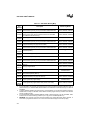
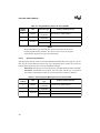
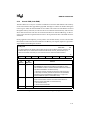
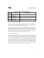
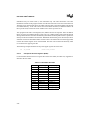
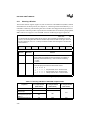
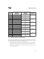
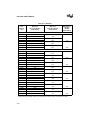
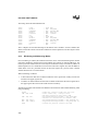
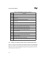
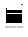
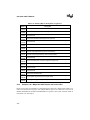
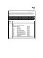
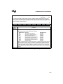
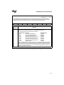
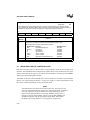
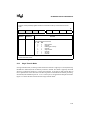
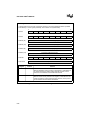
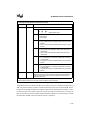
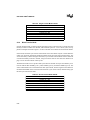
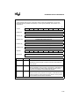
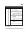
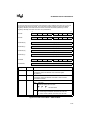
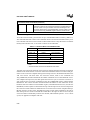
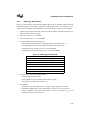
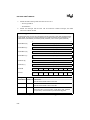
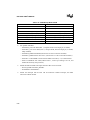
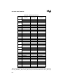
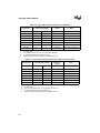
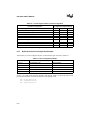
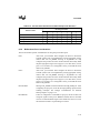
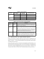
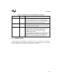
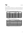
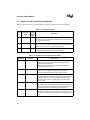
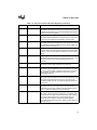
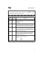
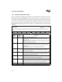
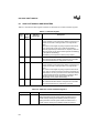
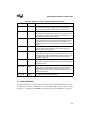
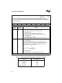
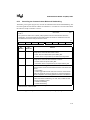
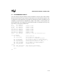
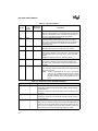
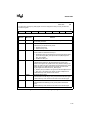
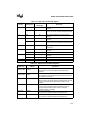
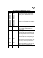
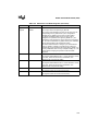
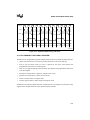
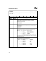
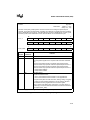
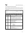
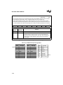
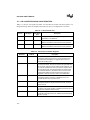
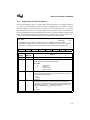
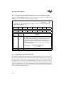
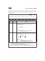
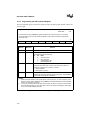
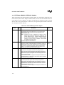
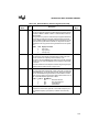
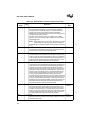
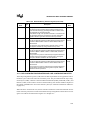
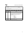
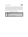
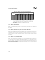
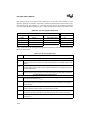
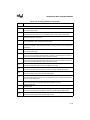
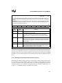
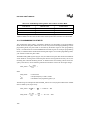
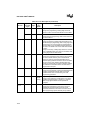
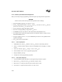
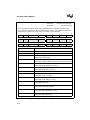
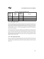
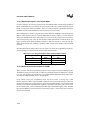
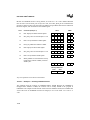
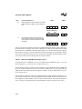
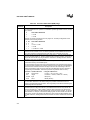
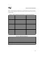
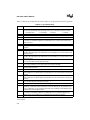
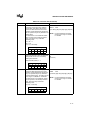
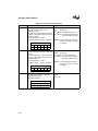
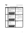
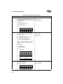
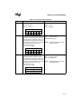
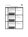
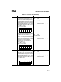
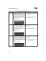
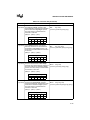
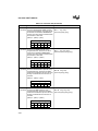
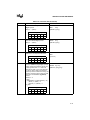
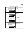
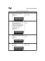
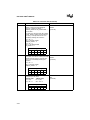
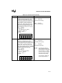
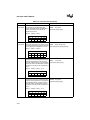
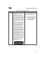
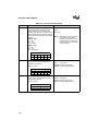
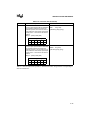
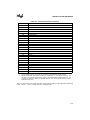
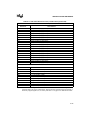
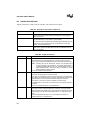
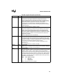
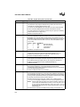
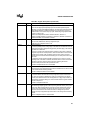
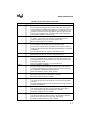
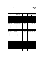
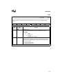
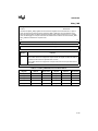
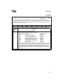
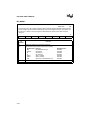
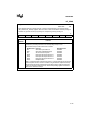
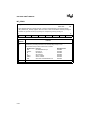
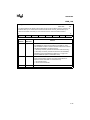
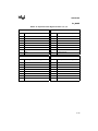
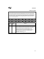
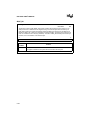
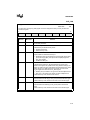
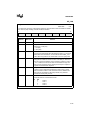
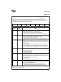
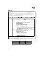
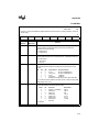
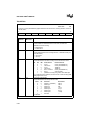
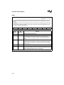
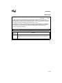
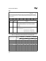
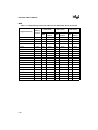
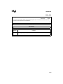
Table 8-2. SSIO Port Control and Status Registers (Continued)
Mnemonic
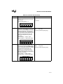
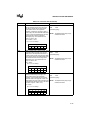
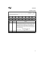
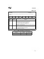
INT_PEND1
Address
0012H
Description
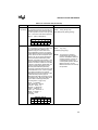
Interrupt Pending 1
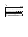
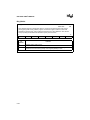
When set, SSIO0 indicates a pending channel 0 transfer interrupt.
When set, SSIO1 indicates a pending channel 1 transfer interrupt.
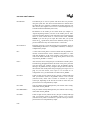
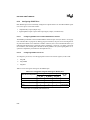
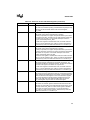
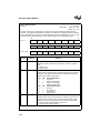
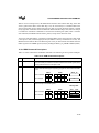
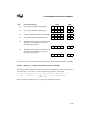
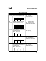
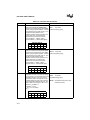
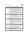
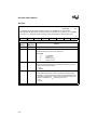
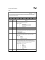
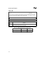
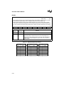
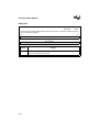
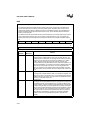
P6_DIR
1FD2H
Port 6 Direction
This register selects the direction of each port 6 pin. Clear P6_DIR.7:4
to configure SD1 (P6.7), SC1 (P6.6), SD0 (P6.5), and SC0 (P6.4) as
high-impedance inputs/open-drain outputs.
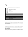
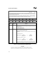
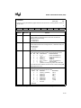
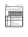
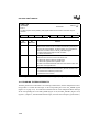
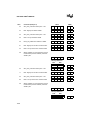
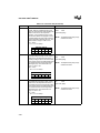
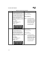
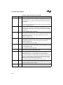
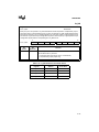
P6_MODE
1FD1H
Port 6 Mode
This register selects either the general-purpose input/output function or
the peripheral function for each pin of port 6. Set P6_MODE.7:4 to
configure SD1 (P6.7), SC1 (P6.6), SD0 (P6.5), and SC0 (P6.4) for the
SSIO.
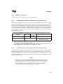
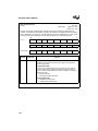
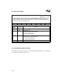
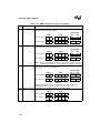
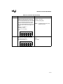
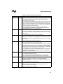
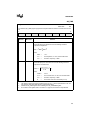
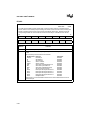
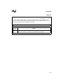
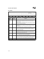
P6_PIN
1FD7H
Port 6 Pin State
Read P6_PIN to determine the current values of SD1 (P6.7), SC1
(P6.6), SD0 (P6.5), and SC0 (P6.4).
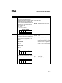
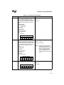
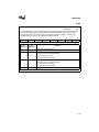
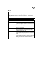
P6_REG
1FD5H
Port 6 Output Data
This register holds data to be driven out on the pins of port 6. For pins
serving as inputs, set the corresponding P6_REG bits; for pins serving
as outputs, write the data to be driven out on the pins to the corresponding P6_REG bits.
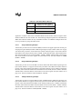
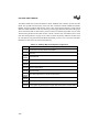
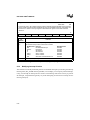
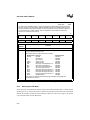
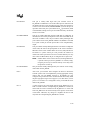
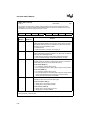
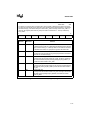
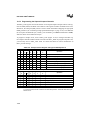
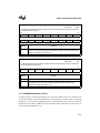
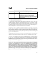
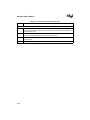
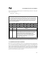
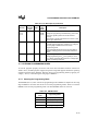
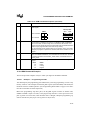
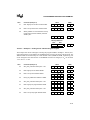
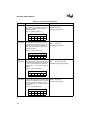
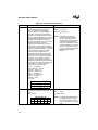
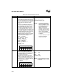
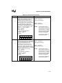
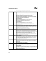
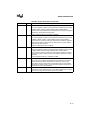
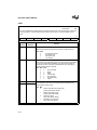
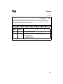
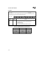
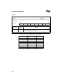
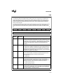
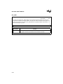
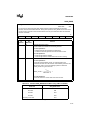
SSIO_BAUD
1FB4H
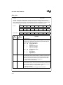
SSIO Baud Rate
This register enables and disables the baud-rate generator and selects
the SSIO baud rate.
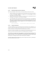
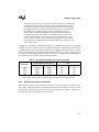
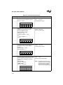
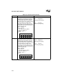
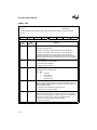
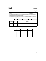
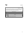
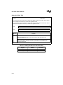
SSIO0_BUF
SSIO1_BUF
1FB0H
1FB2H
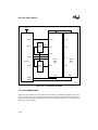
SSIO Receive and Transmit Buffers
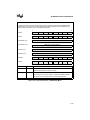
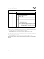
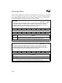
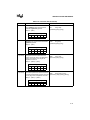
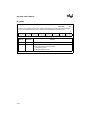
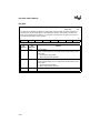
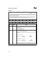
SSIO0_CON
SSIO1_CON
1FB1H
1FB3H
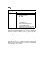
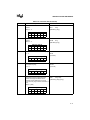
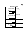
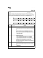
These registers control the communications mode and handshaking
and reflect the status of the SSIO channels.
NOTE:
8.3
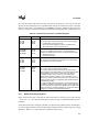
These registers contain either received data or data for transmission,
depending on the communications mode. Data is shifted into this
register from the SDx pin or from this register to the SDx pin, with the
most-significant bit first.
Always write zeros to the reserved bits in these registers.
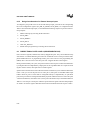
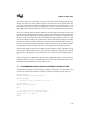
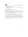
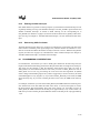
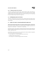
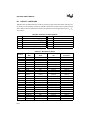
SSIO OPERATION
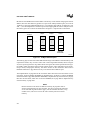
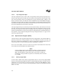
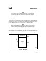
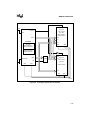
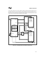
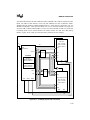
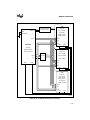
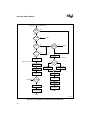
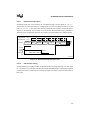
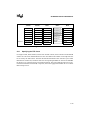
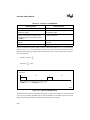
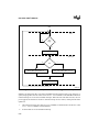
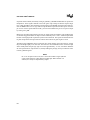
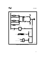
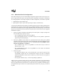
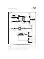
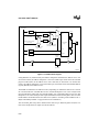
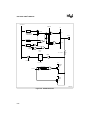
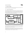
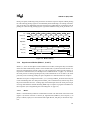
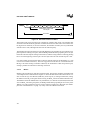
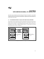
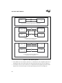
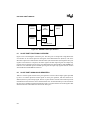
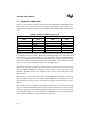
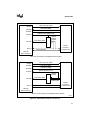
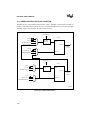
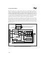
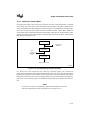
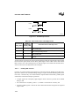
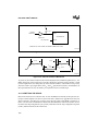
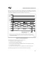
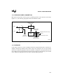
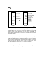
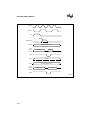
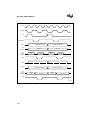
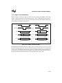
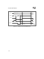
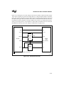
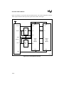
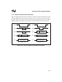
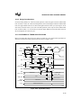
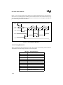
Each SSIO channel can be configured as either master or slave and as either transmitter or receiver, allowing the channels to communicate in several bidirectional, single-byte transfer modes
(Figure 8-2). A master device transmits a clock signal; a slave device receives a clock signal.
8-3