1
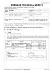
Date: Oct. 14, 2011
RENESAS TECHNICAL UPDATE
1753, Shimonumabe, Nakahara-ku, Kawasaki-shi, Kanagawa 211-8668 Japan
Renesas Electronics Corporation.
Product
Category
Title
MPU & MCU
Document
TN-16C-A204A/E
No.
Descriptions changed in M16C/5M Group,
M16C/57 Group User’s Manual
Information
Category Technical Notification
Rev.
1.00
Lot No.
Applicable
Product M16C/5M and M16C57 Groups
—
Reference
Document
Some specifications of the M16C/5M and M16C57 Groups have been changed. MCU usage and setting
procedures have also been added or changed.
Ä: Indicates the titles in the M16C/5M Group, M16C/57 Group User’s Manual: Hardware Rev.1.10.
1.
1.1
Specification Changes
G1BT Register in Timer S
Ä 18.2.5 Base Timer Register (G1BT)
Do not write to this register.
The G1BT register becomes 0000h when the BTS bit in the G1BCR1 register is set to 0 (base timer reset).
This function works same as before without any change.
2.
2.1
Changes on Usage Note
Interrupt Request When Selecting Time Measurement Function
Ä 18.5.6 Interrupt Request When Selecting Time Measurement Function
When the FSCj bit (j = 0 to 7) in the G1FS register is set to 1 (time measurement function selected), and the
IFEj bit in the G1FE register is also set to 1, the G1IRj bit in the G1IR register, or the IR bit in the ICOCiIC
register (i = 0, 1) or ICOCHjIC register (j = 0 to 3) may become 1 (interrupt requested) after a maximum of
two fBT1 cycles.
When using the IC/OC interrupt i or IC/OC channel j interrupt, set bits FSCj and IFEj to 1, then perform the
following.
(1) Wait for two or more fBT1 cycles.
(2) Set the IR bit in the ICOCiIC register and/or ICOCHjIC register to 0.
(3) Wait for three or more fBT1 cycles after the time measurement function is selected. Set the G1IR
register to 00h after the IR bit in the ICOCiIC register is set to 0.
(c)2011.Renesas Electronics Corporation. All rights reserved.
Page 1 of 2
RENESAS TECHNICAL UPDATE
3.
Date: Oct. 14, 2011
TN-16C-A204A/E
Additions and Changes on Usage and Setting Procedures
3.1
User Boot Mode Program in Flash Memory
Ä 29.11.4.1 User Boot Mode Program in Notes on Flash Memory
Following notes have been added to the user boot mode description:
• When using user boot mode, make sure to allocate the program to be executed to program ROM 2.
• The LVDAS bit in the OFS1 address and bits WDTRCS1 and WDTRCS0 in the OFS2 address are
disabled in boot mode.
• When restarting the MCU in user boot mode after starting it in user boot mode, RAM becomes
undefined.
• If addresses 13FF8h to 13FFBh are all 00h, the MCU does not enter standard serial I/O mode.
Therefore, the programmer or on-chip debugger cannot be connected.
• As the reset sequence differs, the time necessary for starting the program is longer than in single-chip
mode.
• Functions in user boot mode cannot be debugged by the on-chip debugging emulator or full spec
emulator.
• While using user boot mode, do not change the input level of the pin used for user boot entry. However,
if there is a possibility that the input level may change, perform the necessary processes in user boot
mode, then restart the MCU in single-chip mode before the input level changes.
• To use user boot mode after standard serial I/O mode, turn off the power when exiting standard serial I/O
mode, and then turn on the power again (cold start). The MCU enters user boot mode under the right
conditions.
4.
Additions and Changes on Electrical Characteristics
4.1
Oscillator
Ä 31.1.8 Oscillator Electrical Characteristics, 31.4.8 Oscillator Electrical Characteristics
The characteristic of the dedicated 125 kHz on-chip oscillator for the watchdog timer has been added.
Symbol
Dedicated 125 kHz on-chip oscillator for the watchdog timer oscillation
frequency
fWDT
4.2
Standard
Characteristic
Min.
Typ.
Max.
100
125
150
Unit
kHz
Serial Bus Interface
Ä 31.2.2.9 Serial Bus Interface, 31.3.2.9 Serial Bus Interface, 31.5.2.9 Serial Bus Interface, 31.6.2.9 Serial
Bus Interface
The characteristic of td(SSCK-SSIO) now shows the Master and Slave standards independently.
Symbol
td(SSCK-SSIO)
Note:
1.
Measurement
condition
Characteristic
SSO, SSI data output delay time
Standard
Min.
Typ.
Max.
Unit
Master
1
tCYC (1)
Slave
80
ns
1 tCYC = 1/f1 (s)
Page 2 of 2