1
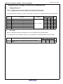
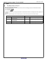
Date: Oct. 14. 2011
RENESAS TECHNICAL UPDATE
1753, Shimonumabe, Nakahara-ku, Kawasaki-shi, Kanagawa 211-8668 Japan
Renesas Electronics Corporation.
Product
Category
Title
MPU & MCU
Document
TN-16C-A205A/E
No.
Descriptions changed in M16C/5L Group,
M16C/56 Group User’s Manual
Information
Category Technical Notification
Rev.
1.00
Lot No.
Applicable
Product M16C/5L and M16C/56 Groups
—
Reference
Document
Some specifications of the M16C/5L and M16C/56 Groups have been changed. MCU usage and setting
procedures have also been added or changed.
Ä: Indicates the titles in the M16C/5L Group, M16C/56 Group User’s Manual: Hardware Rev.1.10.
1.
1.1
Specification Changes
G1BT Register in Timer S
Ä 18.2.5 Base Timer Register (G1BT)
Do not write to this register.
The G1BT register becomes 0000h when the BTS bit in the G1BCR1 register is set to 0 (base timer reset).
This function works same as before without any change.
2.
2.1
Changes on Usage Note
Interrupt Request When Selecting Time Measurement Function
Ä 18.5.6 Interrupt Request When Selecting Time Measurement Function
When the FSCj bit (j = 0 to 7) in the G1FS register is set to 1 (time measurement function selected), and the
IFEj bit in the G1FE register is also set to 1, the G1IRj bit in the G1IR register, or the IR bit in the ICOCiIC
register (i = 0, 1) or ICOCHjIC register (j = 0 to 3) may become 1 (interrupt requested) after a maximum of
two fBT1 cycles.
When using the IC/OC interrupt i or IC/OC channel j interrupt, set bits FSCj and IFEj to 1, then perform the
following.
(1) Wait for two or more fBT1 cycles.
(2) Set the IR bit in the ICOCiIC register and/or ICOCHjIC register to 0.
(3) Wait for three or more fBT1 cycles after the time measurement function is selected. Set the G1IR
register to 00h after the IR bit in the ICOCiIC register is set to 0.
(c)2011.Renesas Electronics Corporation. All rights reserved.
Page 1 of 6
RENESAS TECHNICAL UPDATE
3.
TN-16C-A205A/E
Date: Oct 14. 2011
Additions and Changes on Usage and Setting Procedures
3.1
Flash Memory
3.1.1
User Boot Mode Program
Ä 26.11.4.1 User Boot Mode Program in Notes on Flash Memory
Following notes have been added to the user boot mode description:
• When using user boot mode, make sure to allocate the program to be executed to program ROM 2.
• The LVDAS bit in the OFS1 address and bits WDTRCS1 and WDTRCS0 in the OFS2 address are
disabled in boot mode.
• When restarting the MCU in user boot mode after starting it in user boot mode, RAM becomes
undefined.
• If addresses 13FF8h to 13FFBh are all 00h, the MCU does not enter standard serial I/O mode.
Therefore, the programmer or on-chip debugger cannot be connected.
• As the reset sequence differs, the time necessary for starting the program is longer than in single-chip
mode.
• Functions in user boot mode cannot be debugged by the on-chip debugging emulator or full spec
emulator.
• While using user boot mode, do not change the input level of the pin used for user boot entry. However,
if there is a possibility that the input level may change, perform the necessary processes in user boot
mode, then restart the MCU in single-chip mode before the input level changes.
• To use user boot mode after standard serial I/O mode, turn off the power when exiting standard serial I/O
mode, and then turn on the power again (cold start). The MCU enters user boot mode under the right
conditions.
3.1.2
Procedures When Suspend Function is Enabled
Ä 26.8.1.1 Suspend Function (EW0 Mode), 26.8.2.1 Suspend Function (EW1 Mode)
The procedure for enabling the suspend function has been modified. The modified figures and modifications
are shown below. Post modification and premodification examples of the program flowcharts in EW0 mode
are shown on the next page.
Modified Figures
• Program Flowchart in EW0 Mode (Suspend Function Enabled)
• Block Erase Flowchart in EW0 Mode (Suspend Function Enabled)
• Lock Bit Program Flowchart in EW0 Mode (Suspend Function Enabled)
Modifications
• The timing to set the I flag to 1 (interrupt enabled) has been changed.
• The determination flag used in maskable interrupt routine has been changed from bits FMR32 or FMR33
to the FMR00 bit.
Modified figures
• Program Flowchart in EW1 Mode (Suspend Function Enabled)
• Block Erase Flowchart in EW1 Mode (Suspend Function Enabled)
• Lock Bit Program Flowchart in EW1 Mode (Suspend Function Enabled)
Modification
• The timing to set the I flag to 1 (interrupt enabled) has been changed.
Page 2 of 6
RENESAS TECHNICAL UPDATE
Date: Oct 14. 2011
TN-16C-A205A/E
Post modification
Start
Maskable interrupt (1)
I flag ← 0
Interrupt
disabled
FMR00 = 0 ?
Write 0 and then 1
to the FMR30 bit
Suspend
enabled
Yes
FMR31 ← 1 (3)
Write command code xx41h
to WA address
FMR00 = 1 ?
Write WD0 to WA address
FMR00 = 1 ?
Suspend
request
No
Access flash memory
Yes
Write WD1 to WA address
I flag ← 1
No
Program suspend accepted
Interrupt
enabled (2)
No
Yes
Access flash memory
FMR31 ← 0
Command
restart
REIT
Full status check
Program completed
Notes:
1. In EW0 mode, set the interrupt vector table for interrupts to be used and the interrupt routine in areas other
than flash memory.
2. When interrupts are not used, an instruction to enable interrupts is not necessary.
3. Program is not suspended until td(SR-SUS) elapses after the FMR31 bit is set to 1.
Program Flowchart in EW0 Mode (Suspend Function Enabled)
Premodification
Start
Maskable interrupt (1)
Write 0 and then 1
to the FMR30 bit
Suspend
enabled
Write command code xx41h
to WA address
I flag ← 1
FMR00 = 0 ?
Yes
FMR31 ← 1 (3)
Interrupt
enabled (2)
FMR33 = 1 ?
Suspend
request
No
Access flash memory
Yes
Program suspend accepted
Write WD0 to WA address
Access flash memory
Write WD1 to WA address
No
FMR31 ← 0
FMR00 = 1 ?
Yes
No
Command
restart
REIT
Full status check
Program completed
Notes:
1. In EW0 mode, set the interrupt vector table for interrupts to be used and the interrupt routine in
areas other than flash memory.
2. When interrupts are not used, an instruction to enable interrupts are not necessary.
3. Program is not suspended until td(SR-SUS) elapses after the FMR31 bit is set to 1.
Program Flowchart in EW0 Mode (Suspend Function Enabled)
Page 3 of 6
RENESAS TECHNICAL UPDATE
4.
Date: Oct 14. 2011
TN-16C-A205A/E
Additions and Changes on Electrical Characteristics
4.1
Voltage Detector 2
Ä 27.1.5 Voltage Detector and Power Supply Circuit Electrical Characteristics,
27.4.5 Voltage Detector and Power Supply Circuit Electrical Characteristics
The characteristics of Vdet2_0 to Vdet2_3, and Vdet2_5 to Vdet2_7 for voltage detector 2 have been added.
Symbol
Parameter
Standard
Condition
Min.
Typ.
Max.
Unit
Vdet2_0
Voltage detection level Vdet2_0
3.21
V
Vdet2_1
Voltage detection level Vdet2_1
3.36
V
Vdet2_2
Voltage detection level Vdet2_2
3.51
V
Vdet2_3
Voltage detection level Vdet2_3
3.66
V
Vdet2_5
Voltage detection level Vdet2_5
3.96
V
Vdet2_6
Voltage detection level Vdet2_6
4.10
V
Vdet2_7
Voltage detection level Vdet2_7
4.25
V
4.2
When VCC is falling
Oscillator
Ä 27.1.6 Oscillator Electrical Characteristics, 27.4.6 Oscillator Electrical Characteristics
The characteristic of the dedicated 125 kHz on-chip oscillator for the watchdog timer has been added.
Symbol
fWDT
Characteristic
Dedicated 125 kHz on-chip oscillator for the watchdog timer oscillation
frequency
Standard
Min.
Typ.
Max.
100
125
150
Unit
kHz
Page 4 of 6
RENESAS TECHNICAL UPDATE
4.3
Date: Oct 14. 2011
TN-16C-A205A/E
Hysteresis VT+-VT- for TA0IN and others
Ä 27.2.1 Electrical Characteristics, 27.5.1 Electrical Characteristics (VCC = 5 V)
The maximum value of the following VT+-VT- hysteresis has been changed.
Standard
Symbol
Parameter
VT+-VT-
Hysteresis
Measuring Condition
TA0IN to TA4IN, TB0IN to TB2IN, INT0 to INT5,
NMI, ADTRG, CTS0 to CTS3, SCL2, SDA2,
CLK0 to CLK4, TA0OUT to TA4OUT,
KI0 to KI3, RXD0 to RXD4, ZP, IDU, IDW, IDV,
SD, INPC1_0 to INPC1_7, CRX0
Min.
Unit
Max.
Typ.
0.2
Before
After
2.5
0.4VCC
V
Ä 27.3.1 Electrical Characteristics, 27.6.1 Electrical Characteristics (VCC = 3 V)
The maximum value of the following VT+-VT- hysteresis has been changed.
Standard
Symbol
Parameter
VT+-VT-
4.4
Hysteresis
Measuring Condition
Min.
Unit
Max.
Typ.
TA0IN to TA4IN, TB0IN to TB2IN, INT0 to
INT5, NMI, ADTRG, CTS0 to CTS3, SCL2,
SDA2, CLK0 to CLK4, TA0OUT to
TA4OUT, KI0 to KI3, RXD0 to RXD4, ZP,
IDU, IDW, IDV, SD, INPC1_0 to INPC1_7,
CRX0
Before
After
1.8
0.4VCC
V
Pd in Absolute Maximum Rating
Ä 27.4.1 Absolute Maximum Rating
The rated value of Pd for 85°C < Topr ≤ 125°C in K-version has been changed.
Symbol
Pd
4.5
Characteristic
Condition
Power consumption
Rated Value
Unit
Before
After
200
250
85°C < Topr ≤ 125°C
mW
ICC in Electrical Characteristics
Ä 27.6.1 Electrical Characteristics
The typical values have been changed for the ICC in the 3 V K-version when the following measuring conditions
apply.
Symbol
ICC
Parameter
Power supply current
(VCC = 3.0 V to 3.6 V)
In single-chip mode, the
output pins are open and
other pins are VSS
Measuring Condition
Main clock stopped
40 MHz on-chip oscillator stopped
125 kHz on-chip oscillator 125 kHz on-chip oscillator operating
mode
Divide-by-8
FMR22 = FMR23 = 1 (Low-current consumption
read mode)
f(BCLK) = 32 kHz
On ROM
Low power mode
FMR22 = FMR23 = 1 (Low-current consumption
read mode)
Standard
Typ.
Unit
Min.
Max.
Before After
160
150
450
160
500
μA
μA
Page 5 of 6
RENESAS TECHNICAL UPDATE
5.
Date: Oct 14. 2011
TN-16C-A205A/E
Other
5.1
Two-Phase Pulse in Timer S
Ä 1.5 Pin Assignments and others
Two-phase pulse input pins for timer S have been named. Accordingly, the pins are described as follows.
P8_0/TA4OUT/U/TSUDA
P8_1/TA4IN/U/TSUDB
Symbols and names in the timing requirements are described as follows. No changes have been made to the
standard.
Ä 27.2.2.5 Timer S Input, 27.3.2.5 Timer S Input, 27.5.2.5 Timer S Input, 27.6.2.5 Timer S Input
Before
Symbol
Parameter
After
Symbol
Parameter
tw(TSH)
P8_0 (A-phase), P8_1 (B-phase) Input
HIGH Pulse Width
tw(TSH)
TSUDA, TSUDB input high pulse width
tw(TSL)
P8_0 (A-phase), P8_1 (B-phase) Input
LOW Pulse Width
tw(TSL)
TSUDA, TSUDB input low pulse width
tsu(P8_0-P8_1)
P8_1 (B-phase) Input Setup Time
tsu(TSUDA-TSUDB) TSUDB input setup time
tsu(P8_1-P8_0)
P8_0 (A-phase) Input Setup Time
tsu(TSUDB-TSUDA) TSUDA input setup time
Page 6 of 6