1
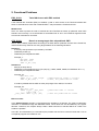
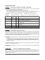
4. Application Hints
CPU_X.H1
Configuration of Registers CPUCON1 and CPUCON2
The default values of registers CPUCON1 and CPUCON2 have been chosen to provide optimized
performance directly after reset. It is recommended
- not to modify the performance related parts of register CPUCON1
- not to modify register CPUCON2, except for test purposes or for enabling specific workarounds
under special conditions (see e.g. problem CPU_X.002 or application hint BREAK_X.H1).
CPUCON2:
reset/recommended value = 8FBBh
CPUCON1:
reset/recommended value = 0..0 0XXX X111; only the 3 lsbs are performance related
Bit Position
Field
Name
CPUCON1.[15:7] 0
CPUCON1.[6:5] VECSC
Value Description
0
00
CPUCON1.4
WDTCTL
0
CPUCON1.3
SGTDIS
0
CPUCON1.2
CPUCON1.1
CPUCON1.0
INTSCXT
BP
ZCJ
1
1
1
CPU_X.H2
; enables several performance features
reserved
scaling factor for vector table, value depends on application,
'00' is compatible to C166 systems
configuration for scope and function of DISWDT/ENWDT
instructions, value depends on application, '0' is compatible
to C166 systems
segmentation enable/disable control, value depends on
application
enable interruptibility of switch context
enable branch prediction unit
enable zero cycle jump function
Special Characteristics of I/O Areas
As an element of performance optimization, the pipeline of the C166S V2 core may perform
speculative read accesses under specific conditions. In case the prediction for the speculative read
was wrong, the read to the actually required location is restarted. While this method is uncritical e.g. for
accesses to non-volatile memories or SRAMs, it may cause problems on devices which do not tolerate
speculative reads (e.g. FIFOs which are advanced on every read access).
No speculative reads are performed in memory areas which are marked as I/O area. This memory
area includes
- the SFR and ESFR space (e.g. with buffers for received data from serial interfaces or A/D results)
- the 4 Kbyte internal I/O area (00'E000h..00'EFFFh), including IIC and SDLM module (on XC161)
- the 2 Mbyte external I/O area (20'0000h..3F'FFFFh), including the TwinCAN module (default: from
20'0000h .. 20'07FFh)
It is therefore recommended to map devices which do not tolerate speculative reads into the 2 Mbyte
external I/O area (20'0000h..3F'FFFFh).
For further special properties of the I/O areas, see section 3.6 (IO Areas) the XC167-32 System Units
User's Manual.
FLASH_X.H1.1
Access to Flash Module after Program/Erase
After the last instruction of a program or erase command, the BUSY bit in register FSR is set to '1'
(status = busy) after a delay of one instruction cycle. When polling the BUSY flag, one NOP or other
instruction which is not evaluating the BUSY flag must be inserted after the last instruction of a
program or erase command.
Errata Sheet XC167CI-32F20F/40F BA
- 11 of 19 –
Mh/Es/UK, V0.1 2004-10-08