1
M16C/6B Group
14. A/D Converter (64-Pin Version Only)
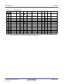
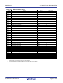
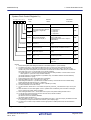
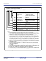
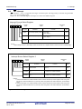
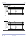
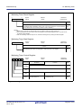
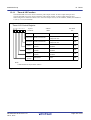
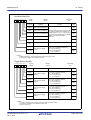
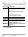
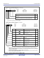
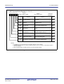
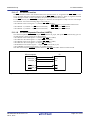
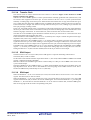
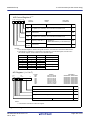
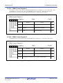
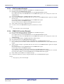
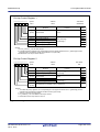
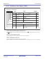
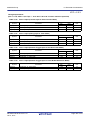
A/D Control Register 0 (1)
b7 b6 b5 b4 b3 b2 b1 b0
Symbol
ADCON0
0 0 0
Address
03D6h
After Reset
00000XXXb
Bit Name
Bit Symbol
Function
RW
b2 b1 b0
CH0
CH1
Analog input pin select bit
CH2
MD0
0
0
0
0
1
1
1
1
0
0
1
1
0
0
1
1
RW
0: Select AN0
1: Select AN1
0: Select AN2
1: Select AN3
0: Select AN4
1: Select AN5
0: Select AN6
1: Select AN7
RW
RW
RW
b4 b3
MD1
A/D operation mode select
bit 0
—
(b5)
Reserved bit
Set to 0
RW
ADST
A/D conversion start flag
0: A/D conversion stop
1: A/D conversion start
RW
CKS0
Frequency select bit 0
Refer to NOTE 2 of the ADCON2 Register
RW
0 0: One-shot mode
RW
NOTE:
1. If the ADCON0 register is rewritten during A/D conversion, the conversion result will be indeterminate.
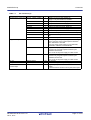
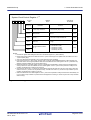
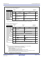
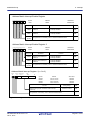
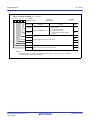
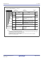
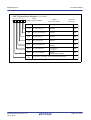
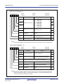
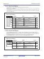
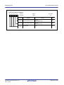
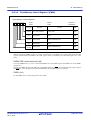
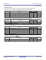
A/D Control Register 1 (1)
b7 b6 b5 b4 b3 b2 b1 b0
0 0 1
Symbol
ADCON1
0
Bit Symbol
Address
03D7h
Bit Name
After Reset
0000X000b
Function
SCAN0
RW
A/D sweep pin select bit
Invalid in one-shot mode
SCAN1
RW
MD2
A/D operation mode select
Set to 0 when one-shot mode is selected
bit 1
—
(b3)
No register bit. If necessary, set to 0. Read as undefined value.
CKS1
Frequency select bit 1
ADSTBY A/D standby bit (2)
—
(b7-b6)
RW
Reserved bits
RW
—
Refer to NOTE 2 of the ADCON2 Register
RW
Set to 1 (A/D operation enabled)
RW
Set to 0
RW
NOTES:
1. If the ADCON1 register is rewritten during A/D conversion, the conversion result will be indeterminate.
2. If the ADSTBY bit is changed from 0 (A/D operation stopped) to 1 (A/D operation enabled), wait for 1
φAD cycle or more before starting A/D conversion.
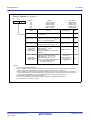
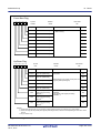
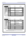
Figure 14.4
Registers ADCON0 and ADCON1 in One-Shot Mode
R01UH0197EJ0120 Rev.1.20
Jul 21, 2011
Page 182 of 331